Serial Lite IV Streaming Intel Stratix 10 FPGA IP Design ......Related Documents The following table...
24
Serial Lite IV Streaming Intel Stratix 10 FPGA IP Design Example User Guide Updated for Intel ® Quartus ® Prime Design Suite: 19.2 IP Version: 1.0.0 Subscribe Send Feedback UG-20241 | 2019.07.01 Latest document on the web: PDF | HTML
Transcript of Serial Lite IV Streaming Intel Stratix 10 FPGA IP Design ......Related Documents The following table...
Serial Lite IV Streaming Intel Stratix10 FPGA IP Design Example UserGuide
Updated for Intel® Quartus® Prime Design Suite: 19.2
IP Version: 1.0.0
SubscribeSend Feedback
UG-20241 | 2019.07.01Latest document on the web: PDF | HTML

Contents
1. About the Serial Lite IV Streaming Intel® Stratix® 10 FPGA IP Design ExampleUser Guide.................................................................................................................3
2. Quick Start Guide............................................................................................................52.1. Design Example Block Diagram............................................................................... 52.2. Hardware and Software Requirements...................................................................... 62.3. Generating the Design............................................................................................6
2.3.1. Design Example Parameters........................................................................72.3.2. Directory Structure.................................................................................... 8
2.4. Compiling and Simulating the Design....................................................................... 92.5. Compiling and Testing the Design...........................................................................10
3. Detailed Description for Serial Lite IV Streaming Design Example................................ 123.1. Features............................................................................................................. 123.2. Traffic Generator..................................................................................................123.3. Traffic Checker.................................................................................................... 133.4. DCFIFO.............................................................................................................. 133.5. Simulation.......................................................................................................... 14
3.5.1. Testbench............................................................................................... 153.6. Hardware Testing.................................................................................................15
3.6.1. Design Setup...........................................................................................163.7. Error Handling.....................................................................................................163.8. Link Debugging Sequence..................................................................................... 173.9. Serial Lite IV Streaming IP Toolkit.......................................................................... 19
3.9.1. Setting Up and Running the Toolkit.............................................................193.9.2. Toolkit GUI Settings................................................................................. 21
4. Document Revision History for the Serial Lite IV Streaming Intel Stratix 10 FPGAIP Design Example User Guide.................................................................................24
Contents
Serial Lite IV Streaming Intel Stratix 10 FPGA IP Design Example User Guide Send Feedback
2
1. About the Serial Lite IV Streaming Intel® Stratix® 10FPGA IP Design Example User Guide
This user guide provides features, usage guidelines, and functional description of theSerial Lite IV Streaming Intel® FPGA IP design examples using E-tile transceivers inIntel Stratix® 10 devices.
Intended Audience
This user guide is intended for:
• Design architects to make IP selection during system level design planning phase.
• Hardware designers when integrating the IP into their system level design.
• Validation engineers during system level simulation and hardware validationphase.
Related Documents
The following table lists other reference documents which are related to the Serial LiteIV Streaming Intel FPGA IP.
Table 1. Related Documents
Reference Description
Serial Lite IV Streaming Intel FPGA IP User Guide This user guide provides IP features, architecturedescription, steps to generate, and guidelines to design theSerial Lite IV Streaming Intel FPGA IP using the E-tiletransceivers.
E-tile Hard IP User Guide: E-tile Hard IP for Ethernet and E-Tile CPRI PHY Intel FPGA IPs
This document describes the features, functionality, andguidelines of the E-Tile Hard IP for Ethernet and E-Tile CPRIPHY Intel FPGA IP cores in Intel Stratix 10 devices.
Intel Stratix 10 Device Data Sheet This document describes the electrical characteristics,switching characteristics, configuration specifications, andtiming for Intel Stratix 10 devices.
E-Tile Transceiver PHY User Guide This document describes the features, functionality, andguidelines of the E-Tile Transceiver PHY in Intel Stratix 10devices.
Acronyms and Glossary
Table 2. Acronym List
Acronym Expansion
CW Control Words
RS-FEC Reed-Solomon Forward Error Correction
PMA Physical Medium Attachment
continued...
UG-20241 | 2019.07.01
Send Feedback
Intel Corporation. All rights reserved. Agilex, Altera, Arria, Cyclone, Enpirion, Intel, the Intel logo, MAX, Nios,Quartus and Stratix words and logos are trademarks of Intel Corporation or its subsidiaries in the U.S. and/orother countries. Intel warrants performance of its FPGA and semiconductor products to current specifications inaccordance with Intel's standard warranty, but reserves the right to make changes to any products and servicesat any time without notice. Intel assumes no responsibility or liability arising out of the application or use of anyinformation, product, or service described herein except as expressly agreed to in writing by Intel. Intelcustomers are advised to obtain the latest version of device specifications before relying on any publishedinformation and before placing orders for products or services.*Other names and brands may be claimed as the property of others.
ISO9001:2015Registered

Acronym Expansion
TX Transmitter
RX Receiver
PAM4 Pulse-Amplitude Modulation 4-Level
PCS Physical Coding Sublayer
MII Media Independent Interface
1. About the Serial Lite IV Streaming Intel® Stratix® 10 FPGA IP Design Example User Guide
UG-20241 | 2019.07.01
Serial Lite IV Streaming Intel Stratix 10 FPGA IP Design Example User Guide Send Feedback
4
2. Quick Start GuideThe Serial Lite IV Streaming Intel FPGA IP provides the capability of generating designexamples for selected configurations.
The Serial Lite IV Streaming Intel FPGA IP design example for Intel Stratix 10 devicesfeatures a simulating testbench and a hardware design that supports compilation andhardware testing. The design example demonstrates loopback mode designs in basicor full mode for duplex configurations.
Figure 1. Development Stages for the Design Example
DesignExample
Generation
Compilation(Simulator)
FunctionalSimulation
Compilation(Quartus Prime)
HardwareTesting
2.1. Design Example Block Diagram
Figure 2. High-level Block Diagram for Intel Stratix 10 Design Examples
DemoManagement
DemoControl
JTAGInterface
SystemConsole
TrafficChecker
DCFIFO
TrafficGenerator
DCFIFO
IOPLLSerial Lite IVStreaming
Duplex
Table 3. Design Example Components
Components Description
Serial Lite IV Streaming IP variation The Serial Lite IV Streaming IP variation accepts data from the trafficgenerator and formats the data for transmission.It also receives data from the link, strips the headers, and presents it tothe traffic checker for analysis.
continued...
UG-20241 | 2019.07.01
Send Feedback
Intel Corporation. All rights reserved. Agilex, Altera, Arria, Cyclone, Enpirion, Intel, the Intel logo, MAX, Nios,Quartus and Stratix words and logos are trademarks of Intel Corporation or its subsidiaries in the U.S. and/orother countries. Intel warrants performance of its FPGA and semiconductor products to current specifications inaccordance with Intel's standard warranty, but reserves the right to make changes to any products and servicesat any time without notice. Intel assumes no responsibility or liability arising out of the application or use of anyinformation, product, or service described herein except as expressly agreed to in writing by Intel. Intelcustomers are advised to obtain the latest version of device specifications before relying on any publishedinformation and before placing orders for products or services.*Other names and brands may be claimed as the property of others.
ISO9001:2015Registered

Components Description
You generate the IP using the parameter editor in the Intel Quartus®
Prime software.
System console The system console is a Intel Quartus Prime tool that provides a user-friendly interface for you to do first-level debugging and monitor statuson the IP, and the traffic generator and checker.
Demo control The demo control module consists of Avalon-MM pipeline bridgesconnected to the transceiver reconfiguration and the demo managementinterfaces separately. The design also instantiates JTAG master, parallelinput/output (PIO), and ISSP (In-system Source and Probe) modules forsystem console debugging purposes.
Demo management The demo management module implements control and status registers(CSRs) to control and monitor the design operation. This includes CSRsto monitor and log errors that occur during the operation.
User clock—IOPLL For Intel Stratix 10 E-tile devices, the design example uses an IOPLL togenerate a user clock for transmitting data into the Serial Lite IVStreaming IP.The design uses the iopll_ref_clk clock signal as an IOPLL referenceclock to connect to the clock generator.The iopll_ref_clk should have the same frequency as thepll_refclk and come from the same clock module.
Traffic generator The traffic generator generates traffic in a deterministic format to verifythat data is transmitted correctly across the link.
Traffic checker The traffic checker performs inspections to verify that the received dataconforms to the expected format.
Dual-clock FIFO (DCFIFO) The DCFIFO blocks handle data streaming and control signals during thecrossing between the user clock domain to the core clock domain andvice-versa.
Related Information
• Traffic Generator on page 12
• Traffic Checker on page 13
• DCFIFO on page 13
2.2. Hardware and Software Requirements
Intel uses the following hardware and software to test the design examples in a Linuxsystem:
• Intel Quartus Prime Pro Edition software version 19.2
• ModelSim*, Xcelium*, NCSim (Verilog only), or VCS*/VCS MX simulator
• Intel Stratix 10 TX Signal Integrity Development Kit (1ST280EY1F55E1VGS1) forhardware testing
2.3. Generating the Design
You can use the IP parameter editor in the Intel Quartus Prime Pro Edition software togenerate the design example.
2. Quick Start Guide
UG-20241 | 2019.07.01
Serial Lite IV Streaming Intel Stratix 10 FPGA IP Design Example User Guide Send Feedback
6

Figure 3. Generating the Design Flow
Start ParameterEditor
Specify IP Variationand Select Device
SelectDesign Parameters
InitiateDesign Generation
Specify Example Design
To generate the design example from the IP parameter editor:
1. In the Tools ➤ IP Catalog, locate and select Serial Lite IV Streaming IntelFPGA IP. The IP parameter editor appears.
2. Specify the parameters for your design.
3. Click the Generate Example Design button.
The software generates all design files in the sub-directories. You need these files torun simulation, compilation, and hardware testing.
2.3.1. Design Example Parameters
The Serial Lite IV Streaming IP parameter editor includes an Example Design tab foryou to specify certain parameters before generating the design example.
Figure 4. Example Design Tab
Table 4. Parameters in the Example Design Tab
Parameter Description
Generate Files for Simulation When selected, the IP generates the necessary files for simulating thedesign example.
Generate Files for Synthesis When selected, the IP generates the synthesis files. Use these files tocompile the design in the Intel Quartus Prime software for hardwaretesting.
continued...
2. Quick Start Guide
UG-20241 | 2019.07.01
Send Feedback Serial Lite IV Streaming Intel Stratix 10 FPGA IP Design Example User Guide
7

Parameter Description
Generate File Format The format of the RTL files for simulation—Verilog or VHDL.
Select Board Supported hardware for design implementation. When you select anIntel FPGA development board, the Target Device is the one thatmatches the device on the Development Kit.If this menu is grayed out, there is no supported board for the optionsthat you select.Stratix 10 TX Signal Integrity Development Kit: This option allowsyou to test the design example on selected Intel FPGA IP developmentkit. This selection automatically selects the Target Device to match thedevice on the Intel FPGA IP development kit. If your board revision has adifferent speed grade, you can change the target device.Custom Development Kit: This option allows you to test the designexample on a third party development kit with Intel FPGA IP device, acustom designed board with Intel FPGA IP device, or a standard IntelFPGA IP development kit not available for selection. You can also select acustom device for the custom development kit.No Development Kit: This option excludes the hardware aspects forthe design example.
Change Target Device Select a different device grade for Intel FPGA IP development kit. Fordevice-specific details, refer to the device datasheet on the Intel FPGAwebsite.
2.3.2. Directory Structure
The Intel Quartus Prime software generates the design example files in the followingfolders:
• <user_defined_design_example_directory>/ed_sim
• <user_defined_design_example_directory>/ed_synth
• <user_defined_design_example_directory>/ed_hwtest
The following diagrams show the directories that contain the generated files for thedesign example.
Figure 5. Directory Structure for Intel Stratix 10 Serial Lite IV Streaming DesignExample
<Design Example>
ed_sim ed_synth ed_hwtest
cadence
mentor
xcelium
synopsys
tb_components
common
system_console
sl4_ip_toolkit
src
seriallite_iv_streaming_demo.qpf
seriallite_iv_streaming_demo.qsf
seriallite_iv_streaming_demo.sdc
2. Quick Start Guide
UG-20241 | 2019.07.01
Serial Lite IV Streaming Intel Stratix 10 FPGA IP Design Example User Guide Send Feedback
8
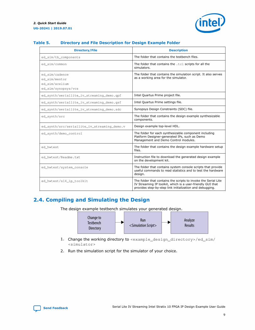
Table 5. Directory and File Description for Design Example Folder
Directory/File Description
ed_sim/tb_components The folder that contains the testbench files.
ed_sim/common The folder that contains the .tcl scripts for all thesimulators.
ed_sim/cadence
ed_sim/mentor
ed_sim/xcelium
ed_sim/synopsys/vcs
The folder that contains the simulation script. It also servesas a working area for the simulator.
ed_synth/seriallite_iv_streaming_demo.qpf Intel Quartus Prime project file.
ed_synth/seriallite_iv_streaming_demo.qsf Intel Quartus Prime settings file.
ed_synth/seriallite_iv_streaming_demo.sdc Synopsys Design Constraints (SDC) file.
ed_synth/src The folder that contains the design example synthesizablecomponents.
ed_synth/src/seriallite_iv_streaming_demo.v Design example top-level HDL.
ed_synth/demo_control The folder for each synthesizable component includingPlatform Designer-generated IPs, such as DemoManagement and Demo Control modules.
ed_hwtest The folder that contains the design example hardware setupfiles.
ed_hwtest/Readme.txt Instruction file to download the generated design exampleon the development kit.
ed_hwtest/system_console The folder that contains system console scripts that provideuseful commands to read statistics and to test the hardwaredesign.
ed_hwtest/sl4_ip_toolkit The folder that contains the scripts to invoke the Serial LiteIV Streaming IP toolkit, which is a user-friendly GUI thatprovides step-by-step link initialization and debugging.
2.4. Compiling and Simulating the Design
The design example testbench simulates your generated design.
Change to Testbench Directory
Run<Simulation Script>
AnalyzeResults
1. Change the working directory to <example_design_directory>/ed_sim/<simulator>
2. Run the simulation script for the simulator of your choice.
2. Quick Start Guide
UG-20241 | 2019.07.01
Send Feedback Serial Lite IV Streaming Intel Stratix 10 FPGA IP Design Example User Guide
9

Table 6. Testbench Simulation Scripts
Simulator File Directory Command
ModelSim <variationname>seriallite4_0_example_design/ed_sim/mentor
do run_tb.tcl
VCS <variationname>seriallite4_0_example_design/ed_sim/synopsys/vcs
sh run_tb.sh
VCS MX <variationname>seriallite4_0_example_design/ed_sim/synopsys/vcsmx
sh run_tb.sh
NCSim <variationname>seriallite4_0_example_design/ed_sim/cadence
sh run_tb.sh
Xcelium <variationname>seriallite4_0_example_design/ed_sim/xcelium
sh run_tb.sh
A successful simulation ends with the following message, "Test Passed." Whensimulation is complete, you can now analyze the results and verify the design.
Figure 6. Sample of Successful Simulation
2.5. Compiling and Testing the Design
The Serial Lite IV Streaming IP parameter editor allows you to compile and run thedesign example on a target development kit.
Compile Designin Quartus Prime
Software
Set up Hardware Program Device Test Designin Hardware
Follow these steps to compile and test the design in hardware:
1. Launch the Intel Quartus Prime Pro Edition software and change the directory toexample_design_dir/ed_synth/ and open theseriallite_iv_streaming_demo.qpf file.
2. Click Processing> Start Compilation to compile the design.
2. Quick Start Guide
UG-20241 | 2019.07.01
Serial Lite IV Streaming Intel Stratix 10 FPGA IP Design Example User Guide Send Feedback
10

The timing constraints for the design example and the design components areautomatically loaded during compilation.
3. Connect the development board to the host computer.
4. Configure the FPGA on the development board using the generatedseriallite_iv_streaming_demo.sof file (Tools> Programmer).
The design example targets the Intel Stratix 10 TX Signal Integrity Development Kit.
The design includes a Synopsys Design Constraints File (SDC) and a Intel QuartusPrime Settings File (QSF) with verified constraints in loopback mode. If you use thedesign example with another device or development board, you may need to updatethe device setting and constraints in the QSF file.
Note: Before downloading the design onto the FPGA, you need to program the clockoscillator on board to the correct transceiver PLL and IOPLL reference clockfrequencies according to the generated design example configuration setting.
2. Quick Start Guide
UG-20241 | 2019.07.01
Send Feedback Serial Lite IV Streaming Intel Stratix 10 FPGA IP Design Example User Guide
11

3. Detailed Description for Serial Lite IV Streaming DesignExample
This design example demonstrates the functionality of data streaming using basic andfull mode.
You can specify the parameters settings of your choice and generate the designexample.
The design example is available only in duplex mode.
3.1. Features
The design example enables you to demonstrate and test the features of the SerialLite IV Streaming IP.
The design example includes the following features:
• Provides basic and full transmission modes
— Basic mode—Pure streaming mode where data is sent without start of packet,empty cycle, and end of packet to increase bandwidth.
— Full mode—This mode sends a burst and sync cycle at the start of frame, anda burst and empty cycle at the end of frame.
• Support for up to 56 Gbps transceiver data rate per lane with a maximum of eightPAM4 lanes in a single link.
• Traffic checker for data verification and lane deskew verification
• System console commands for hardware testing
• Serial Lite IV Streaming IP debugging toolkit
• Debugging sequence
3.2. Traffic Generator
The traffic generator generates traffic in a deterministic format to verify that data istransmitted correctly across the link. The traffic consists of sets of sample words, onefor each lane on the link, that are presented to the source user interface.
If you configure the Serial Lite IV Streaming IP in full mode, the traffic generator alsoasserts the tx_is_usr_cmd signal at random to signify the packet is from user datafor testing purposes. The Serial Lite IV Streaming IP asserts thenum_valid_bytes_eob control signal to signify the number of valid bytes of theburst packet.
UG-20241 | 2019.07.01
Send Feedback
Intel Corporation. All rights reserved. Agilex, Altera, Arria, Cyclone, Enpirion, Intel, the Intel logo, MAX, Nios,Quartus and Stratix words and logos are trademarks of Intel Corporation or its subsidiaries in the U.S. and/orother countries. Intel warrants performance of its FPGA and semiconductor products to current specifications inaccordance with Intel's standard warranty, but reserves the right to make changes to any products and servicesat any time without notice. Intel assumes no responsibility or liability arising out of the application or use of anyinformation, product, or service described herein except as expressly agreed to in writing by Intel. Intelcustomers are advised to obtain the latest version of device specifications before relying on any publishedinformation and before placing orders for products or services.*Other names and brands may be claimed as the property of others.
ISO9001:2015Registered

Figure 7. Traffic Generator Sample Word FormatThis figure shows the format of the sample words generated for each lane.
Word ID Burst Count Word Count
Byte 7 Byte 6 Byte 5 Byte 4 Byte 3 Byte 2 Byte 1 Byte 0
Table 7. Traffic Generator Sample Word Fields
Field Bits Description
Word ID 63–59 Contains a static value to distinguish which 64-bit word on the user interface that thissample was presented on. The Word ID value ranges from 0 to (lanes – 1).
Burst Count 58–32 Tracks the number of bursts used to transfer the sample data. This field value starts withone after reset and is incremented each time the start_of_burst signal is asserted onthe source user interface.
Word Count 31–0 Tracks the number of valid sample words that have been transferred, across all bursts, tothe source user interface.
3.3. Traffic Checker
The traffic checker performs the following inspections to verify that the received dataconforms to the expected format:
• Checks each sample word to verify that the expected word ID was received.
• Checks each sample word to verify that the word count value is higher than theword count value from the last valid sample word.
• Verifies that lane de-skew has been properly performed by validating that theword count and burst count values from the sample word are the same as thevalues received from the adjacent lane.
• If the start_of_burst signal is asserted on the user interface, verifies that theburst count value in the current sample word is higher than the burst count valuefrom the last valid sample word. Otherwise, it verifies that the burst count valuehas not changed.
3.4. DCFIFO
The design uses two DCFIFO blocks at both TX and RX paths.
The DCFIFO blocks handle data streaming and control signals during the crossingbetween the user clock domain to the core clock domain and vice-versa.
Table 8. TX and RX DCFIFO Configuration
Parameter Value
lpm_width (Number of lanes x 64)+21
lpm_numwords 64
The format of the data that passes through the FIFO is similar to format generated bythe traffic generator.
3. Detailed Description for Serial Lite IV Streaming Design Example
UG-20241 | 2019.07.01
Send Feedback Serial Lite IV Streaming Intel Stratix 10 FPGA IP Design Example User Guide
13

Figure 8. Data Format
Word ID Burst Count Word Count
Byte 7 Byte 6 Byte 5 Byte 4 Byte 3 Byte 2 Byte 1 Byte 0
Table 9. Control SignalsThe table lists how the IP concatenates the TX and RX control signals with the data bus signals and passesthrough the data.
Control DCFIFO DataOut Bit
Signal Description
[20] tx_valid
rx_valid
Indicates TX or RX data is valid for Full and Basicmodes.
[19] tx_start_of_packet
rx_start_of_packet
Indicates the start of a TX or RX data packet.For Full mode only.
[18] tx_end_of_packet
rx_end_of_packet
Indicates the end of a TX or RX data packet.For Full mode only.
[17:10] tx_channel
rx_channel
The channel number for data being transmitted orreceived on the current cycle number.For Full mode only.
[9:5] tx_empty
rx_empty
Indicates the number of non-valid words in the finalburst of the TX or RX data.For Full mode only.
[4:1] tg_tx_num_valid_bytes_eob
tc_rx_num_valid_bytes_eob
Indicates the number of valid bytes in the last wordof the final burst.For Full mode only.
[0] tg_tx_is_usr_cmd
tc_rx_is_usr_cmd
Initiates a user-defined information cycle.• Full mode: Must coincide with
tx_startofpacket or rx_startofpacket• Basic mode: Not supported.
Related Information
• FIFO Intel FPGA IP User Guide
• Serial Lite Streaming Intel FPGA IP Interface Signals
3.5. Simulation
The simulation test cases demonstrate continuous streaming of 10,000 sample datafrom the traffic generator to the Serial Lite IV Streaming TX core, and externallyloopback to the RX core.
The simulation test case performs the following steps:
1. Initializes and configures Serial Lite IV Streaming IP, traffic generator and trafficchecker.
2. Traffic generator generates data and starts data transmission.
3. Logs and displays link up status and burst information.
4. Traffic checker verifies received data and stops transmission.
5. Testbench logs and displays test result and test information.
3. Detailed Description for Serial Lite IV Streaming Design Example
UG-20241 | 2019.07.01
Serial Lite IV Streaming Intel Stratix 10 FPGA IP Design Example User Guide Send Feedback
14
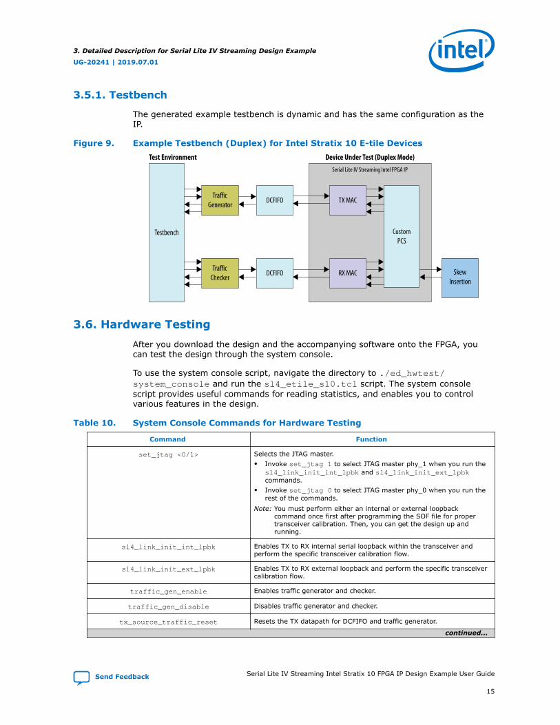
3.5.1. Testbench
The generated example testbench is dynamic and has the same configuration as theIP.
Figure 9. Example Testbench (Duplex) for Intel Stratix 10 E-tile Devices
Testbench
Serial Lite IV Streaming Intel FPGA IP
TrafficGenerator
TrafficChecker
DCFIFO TX MAC
RX MAC SkewInsertion
Device Under Test (Duplex Mode)Test Environment
DCFIFO
CustomPCS
3.6. Hardware Testing
After you download the design and the accompanying software onto the FPGA, youcan test the design through the system console.
To use the system console script, navigate the directory to ./ed_hwtest/system_console and run the sl4_etile_s10.tcl script. The system consolescript provides useful commands for reading statistics, and enables you to controlvarious features in the design.
Table 10. System Console Commands for Hardware Testing
Command Function
set_jtag <0/1> Selects the JTAG master.• Invoke set_jtag 1 to select JTAG master phy_1 when you run the
sl4_link_init_int_lpbk and sl4_link_init_ext_lpbkcommands.
• Invoke set_jtag 0 to select JTAG master phy_0 when you run therest of the commands.
Note: You must perform either an internal or external loopbackcommand once first after programming the SOF file for propertransceiver calibration. Then, you can get the design up andrunning.
sl4_link_init_int_lpbk Enables TX to RX internal serial loopback within the transceiver andperform the specific transceiver calibration flow.
sl4_link_init_ext_lpbk Enables TX to RX external loopback and perform the specific transceivercalibration flow.
traffic_gen_enable Enables traffic generator and checker.
traffic_gen_disable Disables traffic generator and checker.
tx_source_traffic_reset Resets the TX datapath for DCFIFO and traffic generator.
continued...
3. Detailed Description for Serial Lite IV Streaming Design Example
UG-20241 | 2019.07.01
Send Feedback Serial Lite IV Streaming Intel Stratix 10 FPGA IP Design Example User Guide
15
Command Function
rx_sink_traffic_reset Resets the RX datapath for DCFIFO and traffic checker.
read_error_statistics Displays the error statistics.
continuous_mode_en Resets the TX and RX core (MAC and PHY) and enables the trafficgenerator to generate continuous (single continuous data generation)traffic stream. This setting is identical to the setting when running withtraffic_gen_enable command.
burst_mode_en Resets the TX and RX core (MAC and PHY) and enables the trafficgenerator to generate a burst (multiple burst packet data generation)traffic stream.
In additional to this command script, you can also use the Serial Lite IV Streaming IPtoolkit for more feasible visual and troubleshooting purposes on the real-timehardware running link operation.
Related Information
Serial Lite IV Streaming IP Toolkit on page 19
3.6.1. Design Setup
The design example targets the Intel Stratix 10 TX Transceiver Signal IntegrityDevelopment Kit.
The design includes an SDC script as well as a QSF file with verified constraints inloopback mode. If you use the design example with another device or developmentboard, you may need to update the device setting and constraints in the QSF file.
3.7. Error Handling
The Serial Lite IV Streaming IP detects error conditions, and the behaviors in responseto these error conditions.
Table 11. Error Condition Behavior
Signal Width Location Direction Clock Domain Error Indication
tx_error[4:0] 5 Top-levelsignal
Output tx_core_clkout This vector indicates theerror condition of the TXpath.
rx_error[((2*n)+2):0]
(2*n)+2 Top-levelsignal
Output rx_core_clkout When asserted, indicatesthat error conditions occurin the RX datapath.• [(2*n+1):n+2] =
Indicates PCS error forspecific lane.
• [n+1]= Indicates datais forwarded to theuser logic when userlogic is not ready.
• [n] = Indicates loss ofalignment.
• [(n-1):0] = Unused.
continued...
3. Detailed Description for Serial Lite IV Streaming Design Example
UG-20241 | 2019.07.01
Serial Lite IV Streaming Intel Stratix 10 FPGA IP Design Example User Guide Send Feedback
16

Signal Width Location Direction Clock Domain Error Indication
wrfull 1 Top-level RXDCFIFOsignal
Output RX user clock This vector indicates thewrite domain buffer is fulland cannot accept data.
rdfull 1 Top-level RXDCFIFOsignal
Output RX user clock This vector indicates theread domain buffer is fulland cannot accept data.
adaptation_fifo_full
1 Top-level TXDCFIFOsignal
Output TX user clock This vector indicates thewrite domain buffer is fulland cannot accept data.
Related Information
FIFO Intel FPGA IP User Guide
3.8. Link Debugging Sequence
The Serial Lite IV Streaming IP provides a link debugging sequence for TX and RX thatyou can use when debugging your design.
Figure 10. TX Link Debugging Flowchart
Start
No
Yes Yes
No
Yes Note: If rx_link_up status = 0, you need to debug the RX link.
No
tx_link_upAsserted?
* Resets = tx_pcs_fec_phy_reset_n, rx_pcs_fec_phy_reset_n, and reconfig_reset
Check Transceiver Reference Clock
Check if tx_serial_data and rx_serial_data are connected
Check if the resets* are out of reset for at least 10 clock cycles
Check rx_link_up Status
No
pll_lockedAsserted?
phy_tx_lanes_stableAsserted?
phy_ehip_readyAsserted?
3. Detailed Description for Serial Lite IV Streaming Design Example
UG-20241 | 2019.07.01
Send Feedback Serial Lite IV Streaming Intel Stratix 10 FPGA IP Design Example User Guide
17

Table 12. TX Link Debugging Signals
Signal Location Description
tx_link_up Top-level TX signal The IP asserts this signal to indicate that theinitialization sequence is complete, and the IP isready to transmit the data.
tx_pll_locked Top-level PHYsignal
This active-high signal indicates that the transceiversare locked to the reference clock.
phy_tx_lanes_stable Top-level PHYsignal
The IP asserts this signal when TX datapath is readyto send data.
phy_ehip_ready[(n*2)-1:0] Top-level PHYsignal
The IP asserts this signal after thetx_pcs_fec_phy_reset_n andtx_pcs_fec_phy_reset_n signals deassert toindicate that the custom PCS has completed internalinitialization and is ready for transmission.
Figure 11. RX Link Debugging Flowchart
Start
No
Yes Yes
No No
rx_link_upAsserted?
* Resets = tx_pcs_fec_phy_reset_n, rx_pcs_fec_phy_reset_n, and reconfig_reset
Check Transceiver Reference Clock
Check if tx_serial_data and rx_serial_data are connected
Check if the resets* are out of reset for at least 10 clock cycles
No
phy_rx_pcs_readyAsserted?
phy_rx_block_lockAsserted?
phy_ehip_readyAsserted?
Yes RX Ready to Receive Data
3. Detailed Description for Serial Lite IV Streaming Design Example
UG-20241 | 2019.07.01
Serial Lite IV Streaming Intel Stratix 10 FPGA IP Design Example User Guide Send Feedback
18

Table 13. RX Link Debugging Signals
Signal Location Description
rx_link_up Top-level RX signal The IP asserts this signal to indicate that theinitialization sequence is complete, and the IP isready to receive data.
phy_rx_pcs_ready[(n*2)-1:0] Top-level PHYsignal
The IP asserts this signal when RX datapath is readyto receive data.
phy_rx_block_lock[(n*2)-1:0] Top-level PHYsignal
The IP asserts this signal to indicate the 66b blockalignment has completed for the lanes.
Related Information
Serial Lite Streaming Intel FPGA IP Interface Signals
3.9. Serial Lite IV Streaming IP Toolkit
The Serial Lite IV Streaming IP toolkit is an inspection tool that continuously monitorsthe status of a Serial Lite IV Streaming IP link and provides step by step guide on theIP link initialization sequences.
The Serial Lite IV Streaming IP toolkit mainly monitors the following:
• MAC link up status
• Hardened Custom PCS lane alignment status
• Clock data recovery (CDR) lock
• Traffic generator and checker statistics
• Forward Error Correction (FEC) statistics
The IP link initialization sequences guide also includes CSRs to monitor and log errorsthat occur during the operation.
Note: Because the Serial Lite IV Streaming IP toolkit gives out real-time link status throughhardened custom PCS core registers and MAC output ports, you can only use thetoolkit with the design files generated when you configure the design examples..
Related Information
• E-Tile Transceiver PHY User Guide: RS-FEC Registers
• E-Tile Transceiver PHY User Guide
3.9.1. Setting Up and Running the Toolkit
To enable the Serial Lite IV Streaming IP toolkit, you must download and run thetoolkit.
To download and run the toolkit, follow these steps:
3. Detailed Description for Serial Lite IV Streaming Design Example
UG-20241 | 2019.07.01
Send Feedback Serial Lite IV Streaming Intel Stratix 10 FPGA IP Design Example User Guide
19

1. Generate the design example after you specify the parameters.
2. In the Intel Quartus Prime Pro Edition software, select Tools ➤ System Consoleto launch the system console.
3. Based on the directory where your design example is generated, use the TCLcommand in the system console to set the current directory in the system consoleto ../ed_hwtest/sl4_ip_toolkit.
4. Then, type the following command in the TCL console window.
toolkit_register sl4_ip_toolkit.toolkit or toolkit_register<full path directory>/sl4_ip_toolkit.toolkit.
5. Click the Launch button from the system console window.
Figure 12. Launch the Serial Lite IV Streaming IP Toolkit
You can start using the toolkit when the design example successfully programs inthe hardware.
When the toolkit is up and running, set JTAG master by following the instructionsgiven in the display window.
3. Detailed Description for Serial Lite IV Streaming Design Example
UG-20241 | 2019.07.01
Serial Lite IV Streaming Intel Stratix 10 FPGA IP Design Example User Guide Send Feedback
20

Figure 13. Setting JTAG Master
Ensure that you specify the same settings as your design example.
3.9.2. Toolkit GUI Settings
The Serial Lite IV Streaming IP toolkit offers an easy-to-manage user interface.
The Serial Lite IV Streaming IP toolkit user interface has three tabs.
• The MAC and PHY tab implements various control and status registers (CSR) forboth the hardened custom PCS core and the MAC soft logic.
• The Traffic Statistics and Bandwidth Performance tab implements variousControl and Status Registers (CSR) for the Demo Management module toconfigure the traffic generator and checker. Additionally, it also provides a real-time bandwidth calculation measurement result based on the traffic modulesinstantiated in the example design.
• The Help tab provides useful next-step troubleshooting information based on theassertion and deassertion of specific status registers or output ports if any errorshappen after the link initialization is executed.
3. Detailed Description for Serial Lite IV Streaming Design Example
UG-20241 | 2019.07.01
Send Feedback Serial Lite IV Streaming Intel Stratix 10 FPGA IP Design Example User Guide
21

Figure 14. MAC and PHY Tab
The MAC and PHY tab shows a step-by-step guide for link initialization and real-timestatus monitoring of a Serial Lite IV Streaming IP link.
The toolkit continuously reads and displays all of the essential status registers relatedto the Serial Lite IV Streaming IP link after you execute the following stages:
1. Click Assert Full System Reset to perform a full system reset.
2. Click Link Initialization to perform link initialization with internal/externalloopback enabled..
3. Click Read PCS Status to poll all corresponding status registers and output portsfrom both hardened custom PCS and MAC soft logic.
4. Click Read FEC Statistics to generate the FEC statistics report after steps 1–3complete successfully and the link is up and running.
Note: The toolkit user interface changes dynamically to illustrate each execution stage.
In case of any failure, the toolkit narrows down to the type of failure based on thevarious status bits, which are based on the register bank or output port from thehardened custom PCS core or MAC soft logic. The corresponding next-step debugginginformation is displayed in the Help tab.
3. Detailed Description for Serial Lite IV Streaming Design Example
UG-20241 | 2019.07.01
Serial Lite IV Streaming Intel Stratix 10 FPGA IP Design Example User Guide Send Feedback
22

Figure 15. Traffic Statistics and Bandwidth Performance Tab
Note: The Sink RX to Source TX option is not available in the current version of the toolkit.
The Traffic Statistics and Bandwidth Performance tab enables you to configureboth the traffic generator and checker in the design example to run in the user-specified traffic mode, and reads traffic statistics. Additionally, the toolkit alsocalculates and displays the real-time effective bandwidth based on the designexample.
Figure 16. Help Tab
The Help tab provides useful next-step debugging information based on the errors orstatus registers reported from the MAC and PCS status in the MAC and PHY tab.
3. Detailed Description for Serial Lite IV Streaming Design Example
UG-20241 | 2019.07.01
Send Feedback Serial Lite IV Streaming Intel Stratix 10 FPGA IP Design Example User Guide
23
4. Document Revision History for the Serial Lite IVStreaming Intel Stratix 10 FPGA IP Design Example UserGuide
Document Version Intel QuartusPrime
IP Version Changes
2019.07.01 19.2 1.0.0 Initial release.
UG-20241 | 2019.07.01
Send Feedback
Intel Corporation. All rights reserved. Agilex, Altera, Arria, Cyclone, Enpirion, Intel, the Intel logo, MAX, Nios,Quartus and Stratix words and logos are trademarks of Intel Corporation or its subsidiaries in the U.S. and/orother countries. Intel warrants performance of its FPGA and semiconductor products to current specifications inaccordance with Intel's standard warranty, but reserves the right to make changes to any products and servicesat any time without notice. Intel assumes no responsibility or liability arising out of the application or use of anyinformation, product, or service described herein except as expressly agreed to in writing by Intel. Intelcustomers are advised to obtain the latest version of device specifications before relying on any publishedinformation and before placing orders for products or services.*Other names and brands may be claimed as the property of others.
ISO9001:2015Registered