1 The only Israeli Semiconductor Foundry Tower Semiconductor.
Semiconductor Manufacturing Technologyby Michael Quirk and Julian Serda
SemiconductorManufacturing
IC FabricatioOverview
1/41
Semiconductorg Technology
Fabrication ProcessOverview
Objectives
1. Draw a diagram showing hosub-micron CMOS IC fab.
2. Give an overview of the sixsort/test area in the wafer fab
3. For each of the 14 CMOS manufacturinprimary purpose.
4. Discuss the key process andmanufacturing step.
2/41
Objectives
how a typical wafer flows in a
major process areas and the fab.manufacturing steps, describe its
equipment used in each CMOS
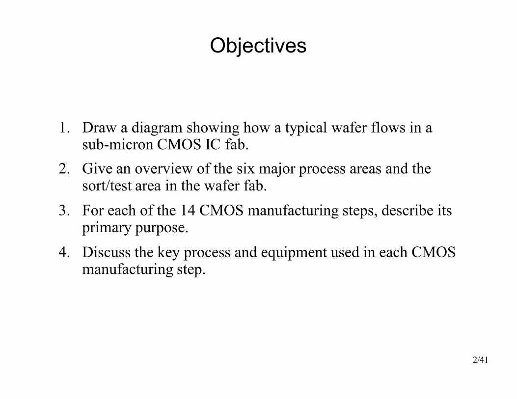
Major Fabrication Steps
Used with permission from
Oxidation(Field oxide)
Silicon substrate
Silicon dioxide
oxygen
Photoresist Coating
photoresist
MaskAlignment
GS D
ActiveRegions
top nitride
S GG
silico
NitrideDeposition
IonImplantation
reoxox S
DG
Scanning ion beam
Oxidation(Gate oxide)
gate
oxygen
PhotoresistStrip
oxide
Ionized oxygen gas
OxideEtch
photoresistoxide
Ionized CF gas4
s in MOS Process Flow
Advanced Micro Devices
Photoresist Develop
oxide
Mask-WaferAlignment and Exposure Photoresist
UV light
Mask
Exposed
exposedphotoresist
nitrideG D
silicon nitride
NitrideDeposition
Contactholes
S DG
ContactEtch
dS rGaiDnMetal
Deposition andEtch
Metal contacts
PolysiliconDeposition
Silane gas
polysilicon
Dopant gas
Oxidationoxide)
e oxide
oxygen
Polysilicon Mask and Etch
oxide
Ionized CCl4 gas
3/41
CMOS Process Flow
• Overview of Areas– Diffusion– Photolithography– Etch– Ion Implant– Thin Films– Polish
• CMOS Manufacturin• Parametric Testing• 6~8 weeks involve
4/41
Process Flow
in a Wafer Fab
Manufacturing Steps
350-step
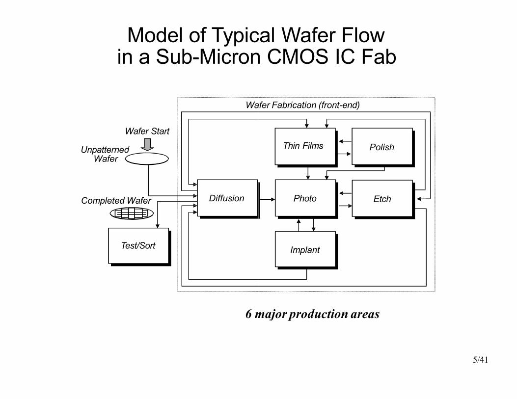
Model of Typicalin a Sub-Micron
Test/Sort
DiffusionCompleted Wafer
UnpatternedWafer
Wafer Start
Wafer Fabrication (fron
6 major
Typical Wafer FlowMicron CMOS IC Fab
5/41
Implant
Etch
Polish
Photo
Thin Films
Wafer Fabrication (front-end)
6 major production areas
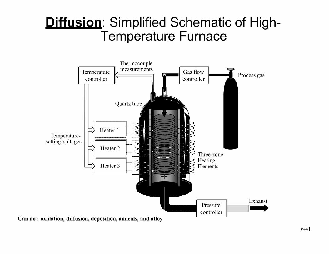
Diffusion: Simplified Temperature
Temperaturecontroller
Heater 1
Heater 2
Heater 3
Quartz tube
Temperature-setting voltages
Thermocouplemeasurements
Can do : oxidation, diffusion, deposition, anneals, and alloy
Simplified Schematic of High-Temperature Furnace
Gas flow controller
Pressurecontroller
6/41
Exhaust
Process gas
Three-zoneHeating Elements
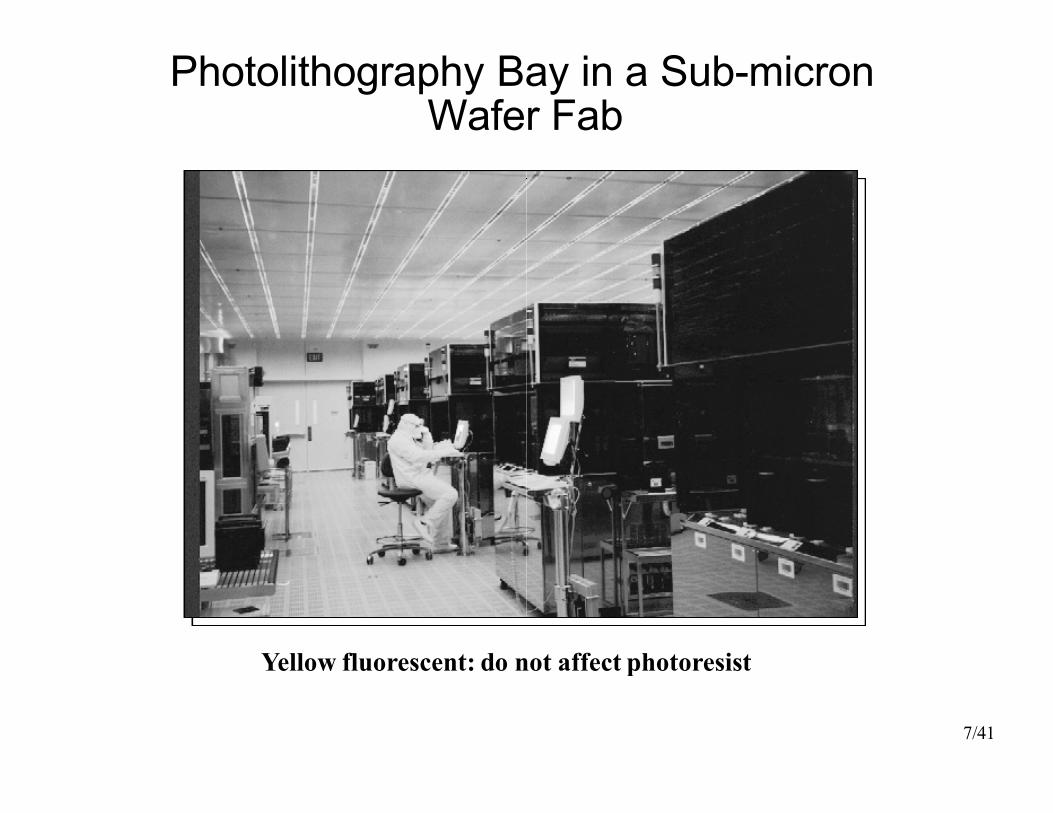
Photolithography Bay Wafer
Yellow fluorescent: do not affect photoresist
Bay in a Sub-micron Wafer Fab
not affect photoresist
7/41
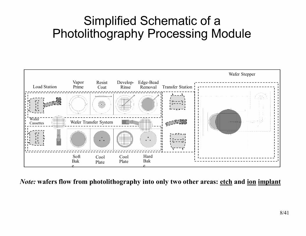
Load StationVaporPrime
Soft Bake
Cool Plate
Cool Plate
Hard Bake
ResistCoat
Develop-Rinse
Edge-BeadRemoval
Wafer Transfer SystemWaferCassettes
Simplified Schematic Photolithography Processing Module
Note: wafers flow from photolithography into
Hard
Transfer StationBead
Removal
Wafer Stepper
Schematic of aProcessing Module
8/41
o only two other areas: etch and ion implant
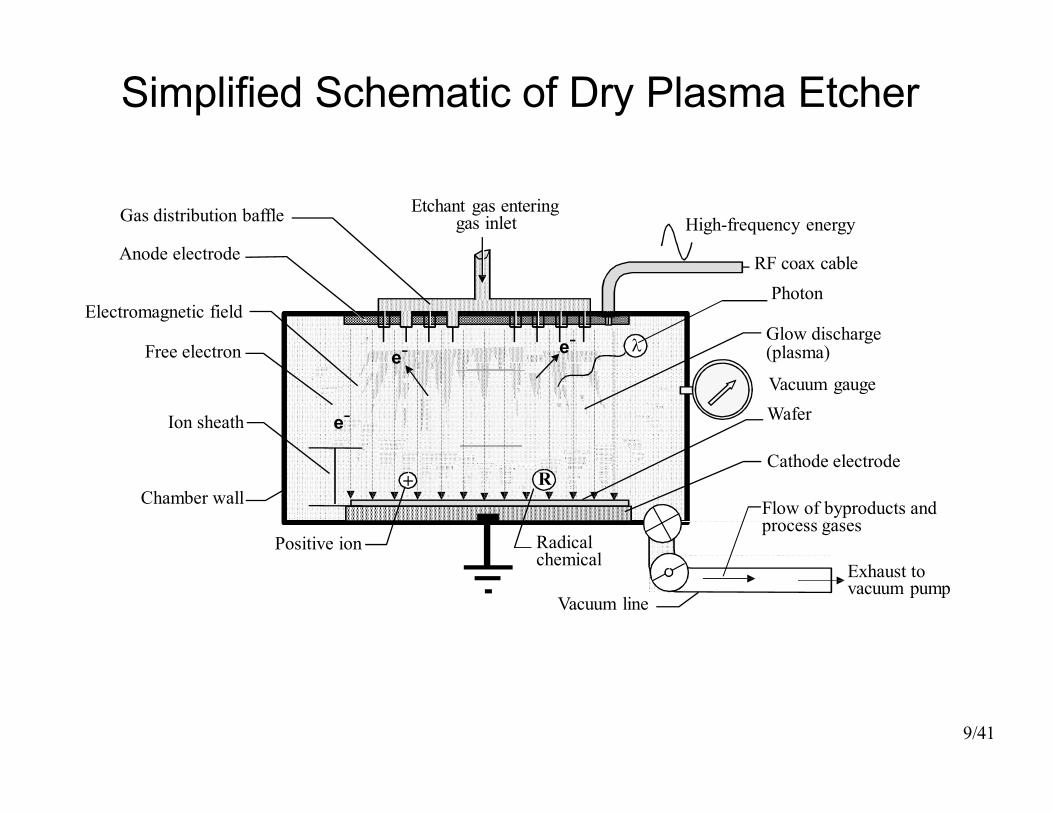
Simplified Schematic of
e-
+
Gas distribution baffle
Anode electrode
Electromagnetic field
Free electron
Ion sheath
Chamber wall
Positive ion
Etchant gas entering gas inlet
e-
of Dry Plasma Etcher
e-
R
RF coax cablePhoton
Glow discharge (plasma)
Vacuum gaugeWafer
9/41
High-frequency energy
Flow of byproducts and process gases
entering
Cathode electrode
Radicalchemical
Vacuum line
Exhaust tovacuum pump
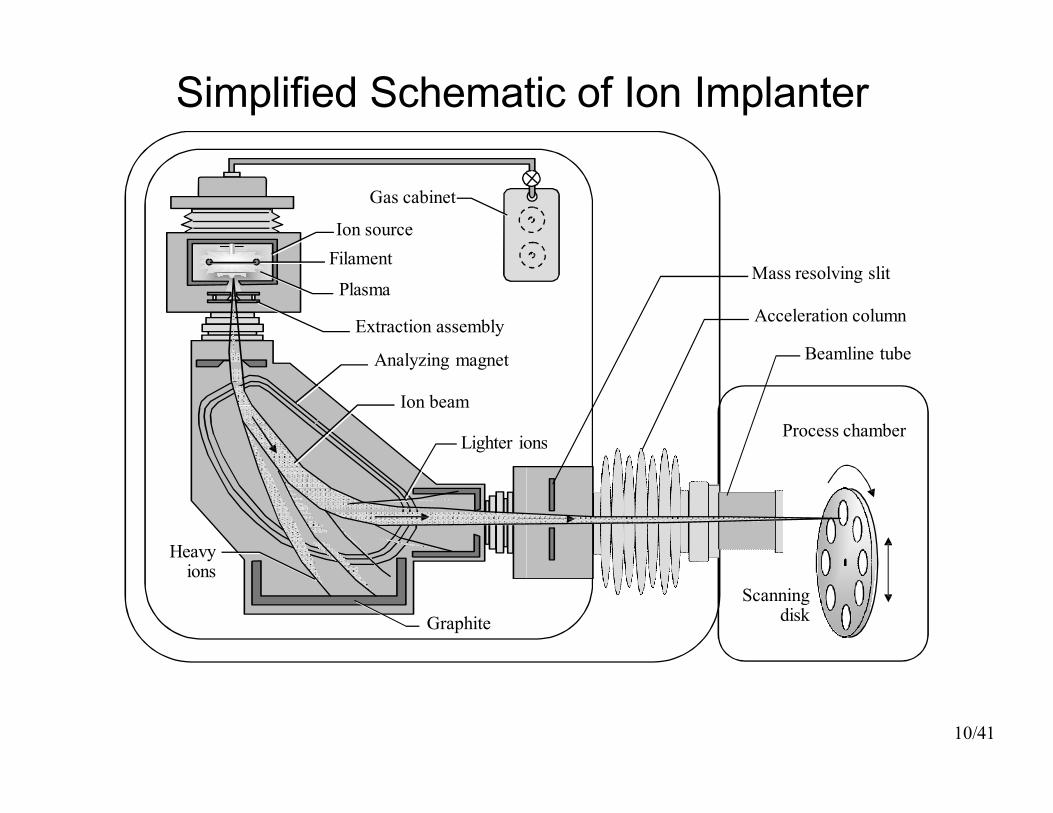
Simplified Schematic
Ion sourceFilament
Plasma
Extraction assembly
Analyzing magnet
Ion beam
Graphite
Heavyions
Gas cabinet
Lighter ions
Schematic of Ion Implanter
10/41
Acceleration column
Beamline tube
Process chamber
Scanningdisk
Mass resolving slit
ions
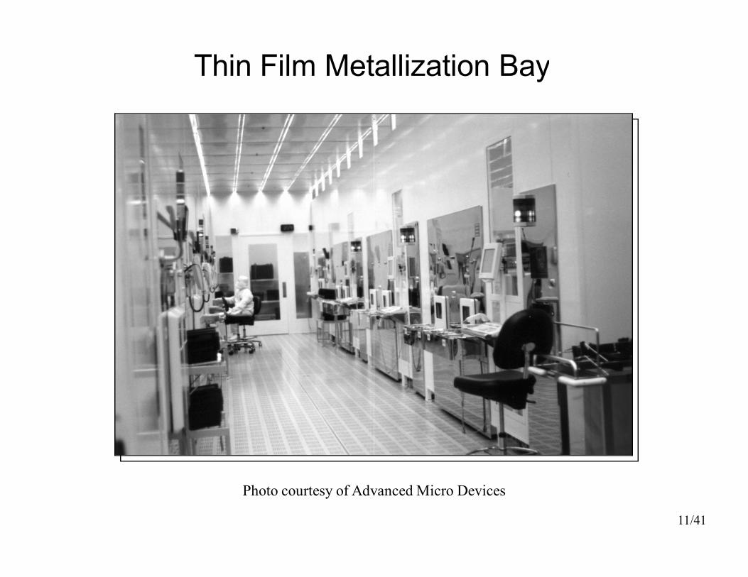
Thin Film Metallization Bay
Photo courtesy of Advance
Film Metallization Bay
Advanced Micro Devices
11/41
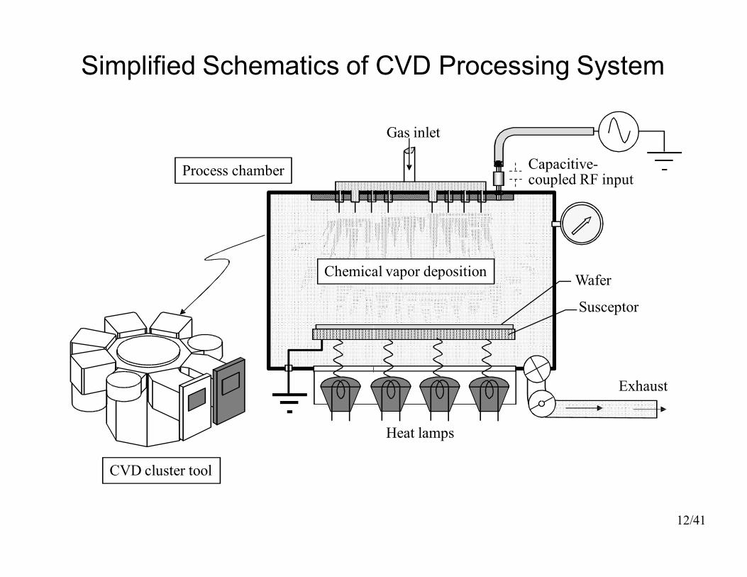
Simplified Schematics of
Chemica
Process chamber
CVD cluster tool
CVD Processing System
Capacitive-coupled RF input
Wafer
Susceptor
Heat lamps
Gas inlet
Exhaust
Chemical vapor deposition
12/41
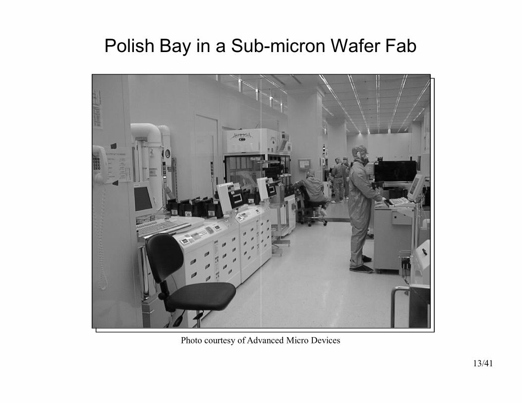
Polish Bay in a Sub
Photo courtesy of Advanced
Sub-micron Wafer Fab
Advanced Micro Devices
13/41
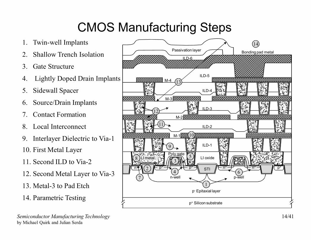
1. Twin-well Implants
2. Shallow Trench Isolation
3. Gate Structure
4. Lightly Doped Drain Implants
5. Sidewall Spacer
6. Source/Drain Implants
7. Contact Formation
8. Local Interconnect
9. Interlayer Dielectric to Via-110. First Metal Layer
11. Second ILD to Via-2
12. Second Metal Layer to Via-3
13. Metal-3 to Pad Etch
14. Parametric Testing
LI metal
Via
n+ 2
7
8
12
Semiconductor Manufacturing Technologyby Michael Quirk and Julian Serda
CMOS Manufacturing StepsPassivation layer Bonding pad metal
p+ Silicon substrate
LI oxide
STI4n-well
6p-well
ILD-1
ILD-2
ILD-3
ILD-4
ILD-5
M-1
M-2
M-3
M-4
Poly gate
1p- Epitaxial layer
p+
ILD-6
Via
p+ p+ n+n+
35
9
10
11
12
13
14
14/41
Manufacturing Steps
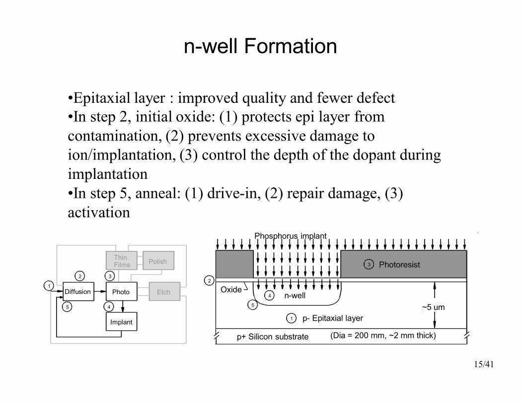
n-well Formation
3
1
2
Photo
Implant
Diffusion
4
Polish
Etch
5
Thin Films
p+ Silicon
Oxide
5
•Epitaxial layer : improved qualit•In step 2, initial oxide: (1) protectcontamination, (2) prevents excessivion/implantation, (3) control thimplantation•In step 5, anneal: (1) drive-in,activation
Phosphoru
2
Formation
~5 um
(Dia = 200 mm, ~2 mm thick)
Photoresist
1
Silicon substrate
p- Epitaxial layer
n-well4
quality and fewer defectprotects epi layer from excessive damage to the depth of the dopant during
(2) repair damage, (3)
Phosphorus implant
15/41
3
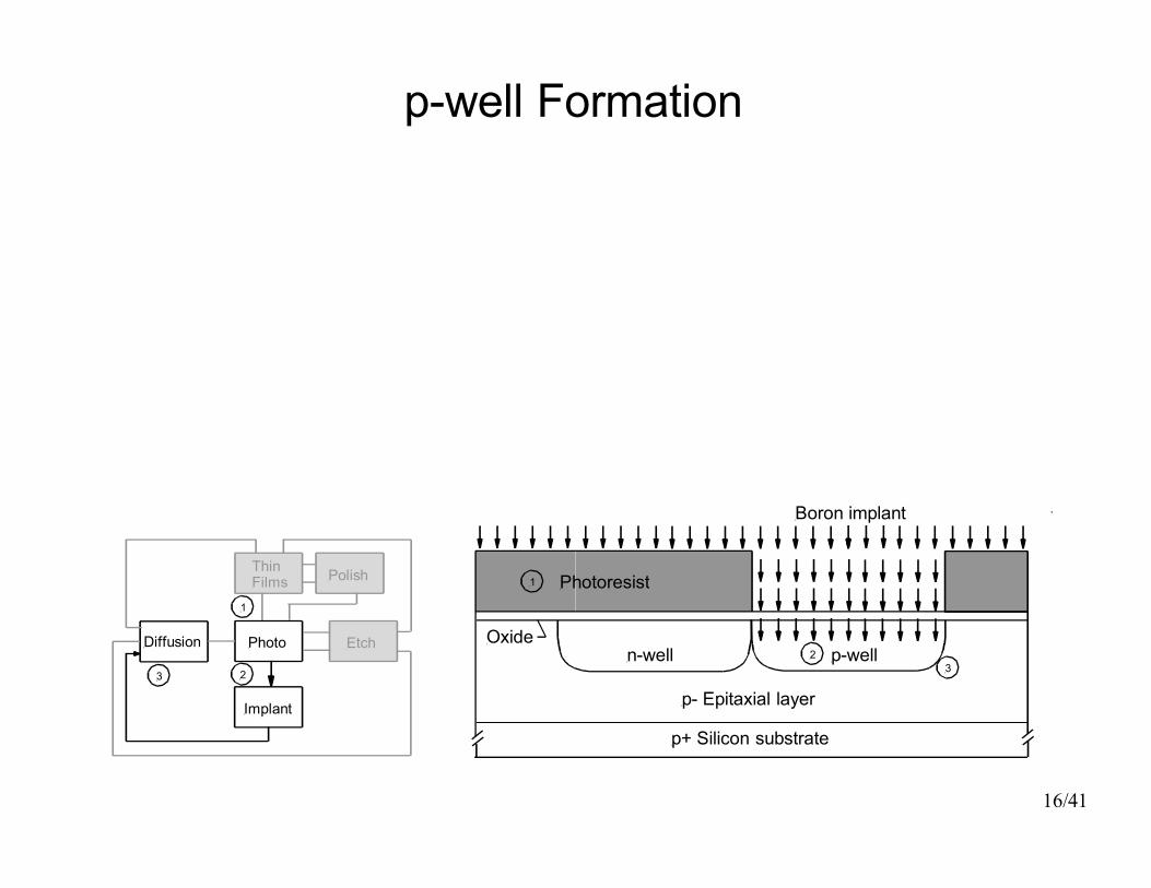
p-well Formation
Thin Films
3
1
2
Photo
Implant
Diffusion
Polish
Etch
Photoresist1
Oxide
Formation
p+ Silicon substrate
Boron implant
Photoresist
p- Epitaxial layer
3n-well 2 p-well
16/41
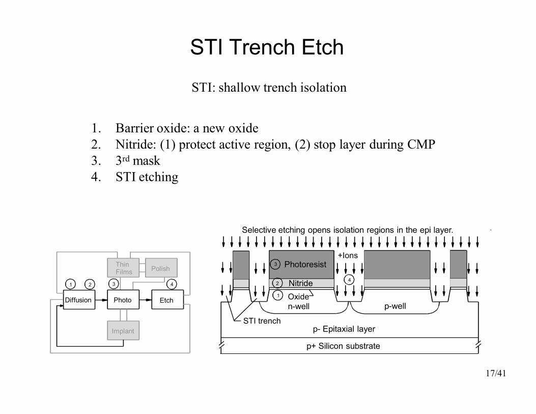
STI Trench Etch
Thin Films
1 2
Diffusion Photo
Polish
Etch
Implant
3 4
Selectiv
STI trench
STI: shallow trench isolation
1. Barrier oxide: a new oxide2. Nitride: (1) protect active region3. 3rd mask4. STI etching
STI Trench Etch
Selective etching opens isolation regions in the epi layer.
+Ions
p+ Silicon substrate
p- Epitaxial layer
n-well p-well
3 Photoresist
2 Nitride 4
1 Oxide
trench
STI: shallow trench isolation
region, (2) stop layer during CMP
17/41
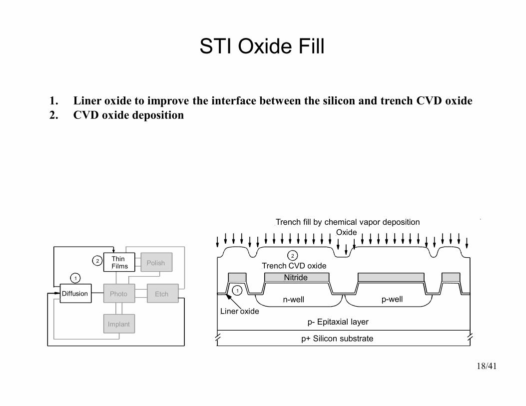
STI Oxide
1
2
Diffusion
Polish
EtchPhoto
Implant
Thin Films
1
Liner oxide
Trenc
1. Liner oxide to improve the interface betwee2. CVD oxide deposition
STI Oxide Fill
p-well
p+ Silicon substrate
Trench fill by chemical vapor depositionOxide
p- Epitaxial layer
n-well
2
NitrideTrench CVD oxide
between the silicon and trench CVD oxide
18/41
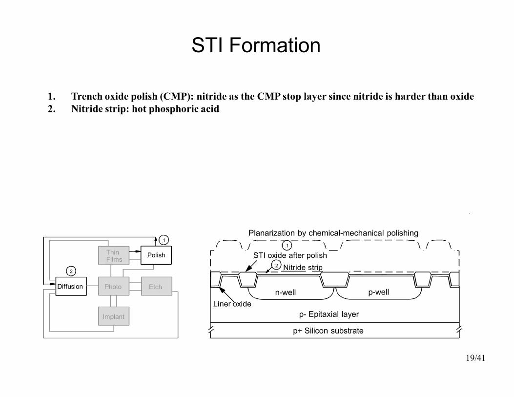
STI Formation
Thin Films
1
2
Diffusion EtchPhoto
Implant
Polish
Planarization
STI
Liner oxide
1. Trench oxide polish (CMP): nitride as the 2. Nitride strip: hot phosphoric acid
Formation
p-well
Planarization by chemical-mechanical polishing1
STI oxide after polish2 Nitride strip
p+ Silicon substrate
p- Epitaxial layer
n-well
CMP stop layer since nitride is harder than oxide
19/41
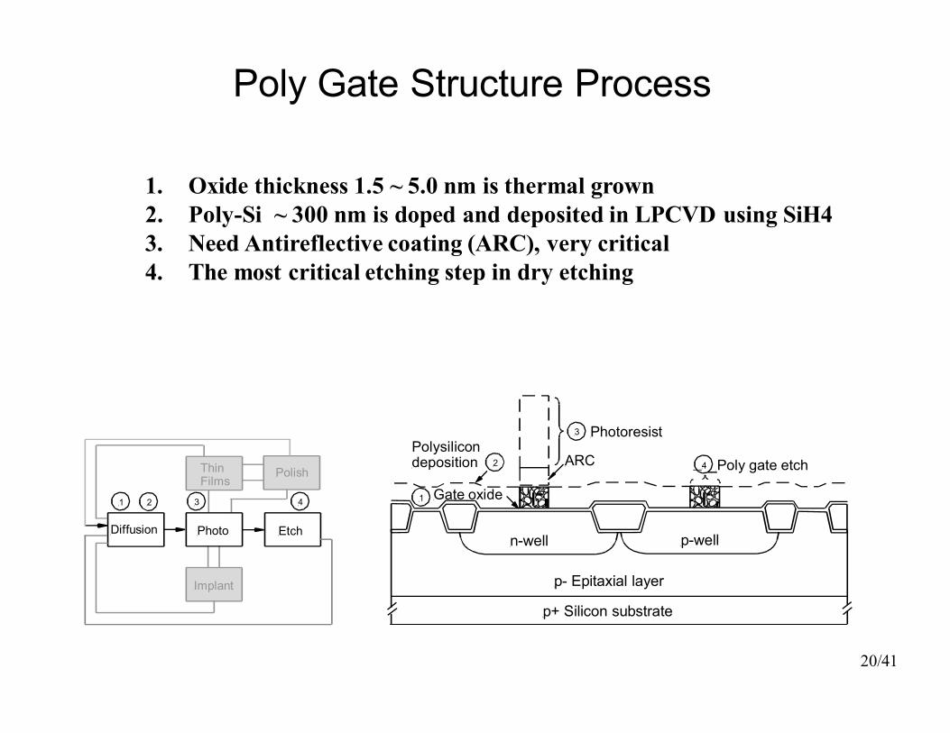
Poly Gate Structure
ThinFilms
1 2
Diffusion EtchPhoto
Implant
Polish
3 4 Gate oxide1
Polysilicon deposition
1. Oxide thickness 1.5 ~ 5.0 nm2. Poly-Si ~ 300 nm is doped and3. Need Antireflective coating (ARC),4. The most critical etching step
Structure Process
p+ Silicon substrate
Gate oxide
2
p- Epitaxial layer
n-well p-well
Polysilicon deposition 4 Poly gate etch
3 Photoresist
ARC
nm is thermal grownand deposited in LPCVD using SiH4(ARC), very critical
step in dry etching
20/41

n LDD
Thin Films
1
2
Diffusion EtchPhoto
Implant
Polish
n-
1. LDD: lightly doped drain to reduce 2. Large mass implant (BF2, instead of
surface helps maintain a shallow junction3. 5th mask
LDD Implant
p+ Silicon substrate
p- Epitaxial layer
n-well p-welln-n-
1 Photoresist mask
2 Arsenic n- LDD implant
lightly doped drain to reduce S/D leakageof B, As instead of P) and amorphous
junction
21/41
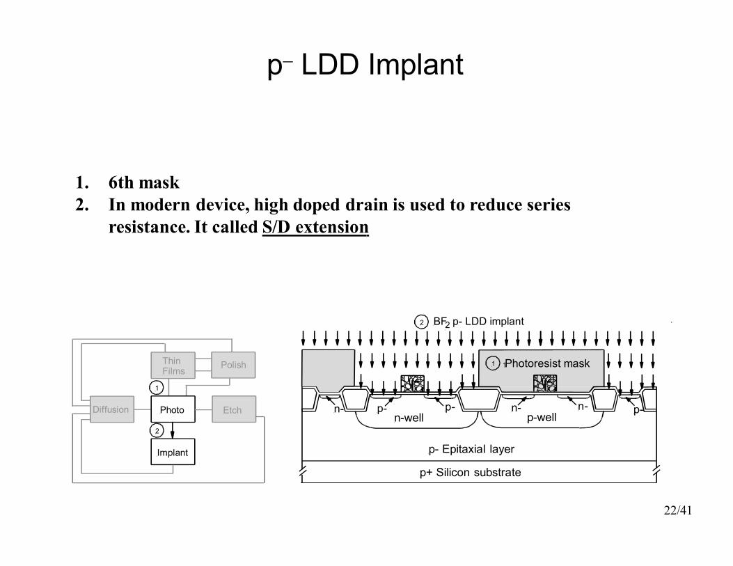
p LDD
1
2
Diffusion EtchPhoto
Implant
PolishThin Films
n-
1. 6th mask2. In modern device, high doped drain
resistance. It called S/D extension
LDD Implant
p+ Silicon substrate
p- Epitaxial layer
n-well p-well
Photoresist Mask1Photoresist mask
p-p-
1
n-n-
2 BF2 p- LDD implant
p-
22/41
drain is used to reduce series extension
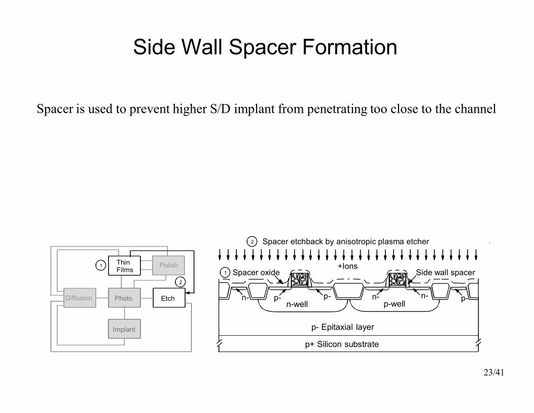
Side Wall Spacer Formation
1
2
Diffusion EtchPhoto
Implant
PolishThin Films 1 Spacer oxide
2 Spacer
n-
Spacer is used to prevent higher S/D implant from penetrating t
Side Wall Spacer Formation
+Ions
p+ Silicon substrate
p- Epitaxial layer
n-well p-wellp-p-
Spacer oxide Side wall spacer
Spacer etchback by anisotropic plasma etcher
p-n-n-
23/41
implant from penetrating too close to the channel
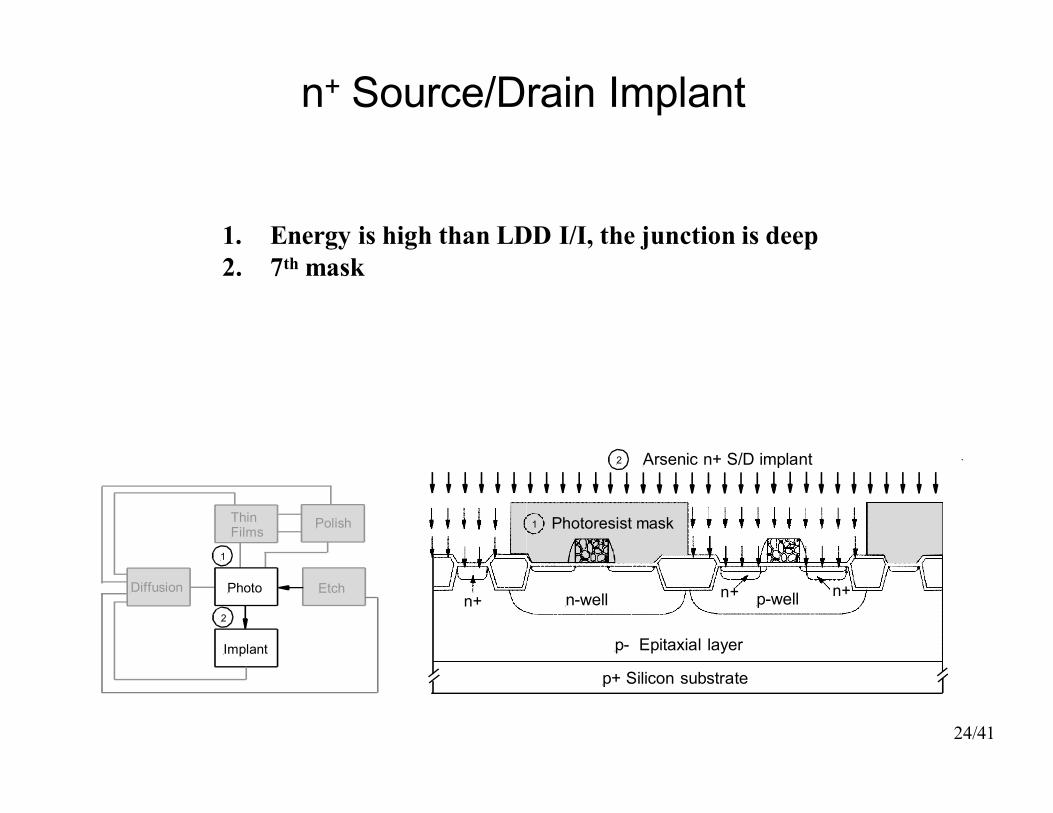
n+ Source/Drain
Thin Films
1
2
Diffusion EtchPhoto
Implant
Polish
n+
1. Energy is high than LDD2. 7th mask
Source/Drain Implant
p+ Silicon substrate
p- Epitaxial layer
n-well p-well
Arsenic n+ S/D implant2
Photoresist mask
24/41
1
n+ n+
LDD I/I, the junction is deep
p+ Source/Drain
1
2
Diffusion EtchPhoto
PolishThin Films
Implant
3n+
1. 8th mask2. Using rapid thermal anneal (RTA)
spreading and to control diffusion
Source/Drain Implant
Boron p+ S/D implant2
p+ Silicon substrate
p+ n+
p- Epitaxial layer
25/41
n-well p-well
Photoresist Mask1Photoresist mask1
p+ n+ p+
(RTA) to prevent dopant diffusion of dopant
Contact Formation
Thin Films
1 2
Diffusion EtchPhoto
Implant
Polish3 Titanium
n+
1. Titanium (Ti) is a good choice forresistivity and good adhesion
2. No mask needed, called self-align3. Using Ar to sputtering metal4. Anneal to form TiSi2, tisilicide5. Chemical etching to remove unreact
selective etching
Contact Formation
2 Tisilicide contact formation (anneal)etch3
Titanium depostion1
p+ n-well p+ n+ p-well n+ p+
p- Epitaxial layer
p+ Silicon substrate
for metal contact due to low
align
unreact Ti, leaving TiSi2, called
26/41
LI Oxide as a Dielectric for Inlaid LI (Damascene)
LI metal
LI oxide
LI: local interconnection
Damascene: a name doped of year ago from a practice that
Dielectric for Inlaid LI Metal (Damascene)
oxide
interconnection
27/41
that began thousands ago by artist in Damascus, Syria
LI Oxide Dielectric
1 Nitride CVD
Diffusion EtchPhoto
Implant
Polish
3
4
21
Thin Films
1. Nitride: protec2. Doped oxide3. Oxide polish4. 9th mask
Dielectric Formation
CVD
p-wellp-well
p- Epitaxial layer
p+ Silicon substrate
Oxide polish
LI oxide
2 Doped oxide CVD
4 LI oxide etch3
28/41
protect active region
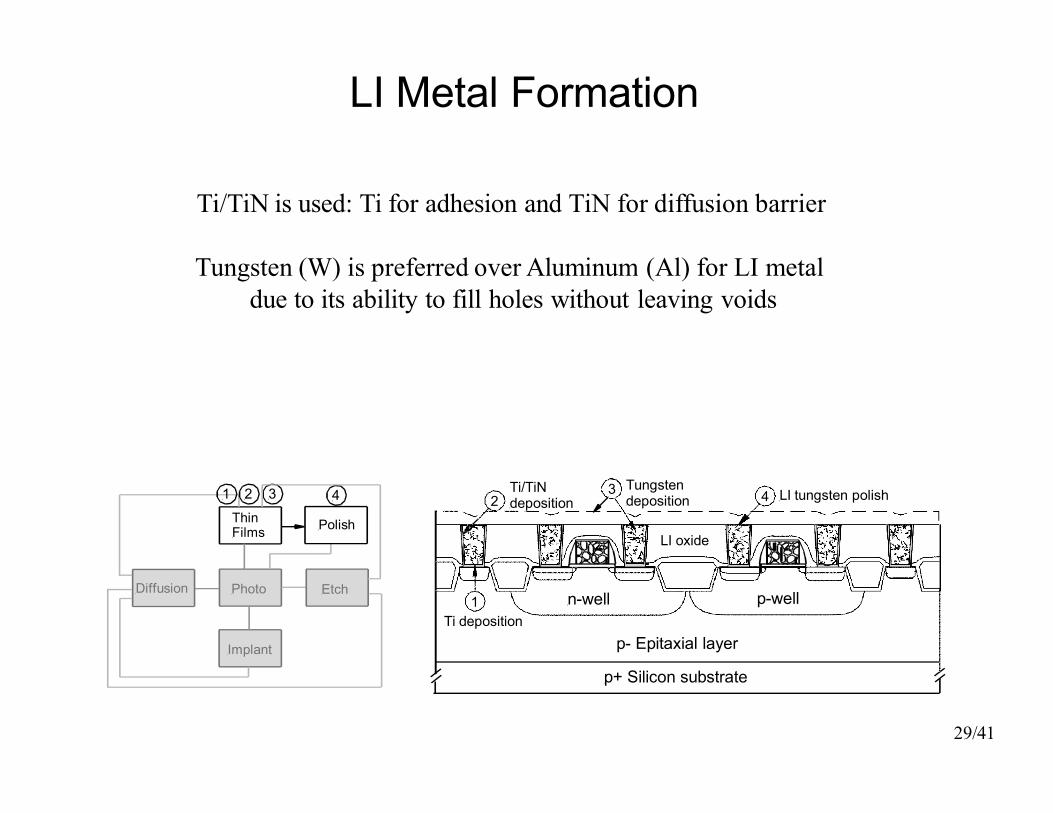
LI Metal Formation
Thin Films
Diffusion Photo
Implant
1 2 3 4
Etch
Polish
Ti/TiN deposition2
1Ti deposition
Ti/TiN is used: Ti for adhesion an
Tungsten (W) is preferred over Aluminumdue to its ability to fill hole
Formation
n-well
LI tungsten polishTungstendeposition
Ti/TiN deposition
3 4
LI oxide
p-well
p- Epitaxial layer
p+ Silicon substrate
29/41
and TiN for diffusion barrier
Aluminum (Al) for LI metalholes without leaving voids
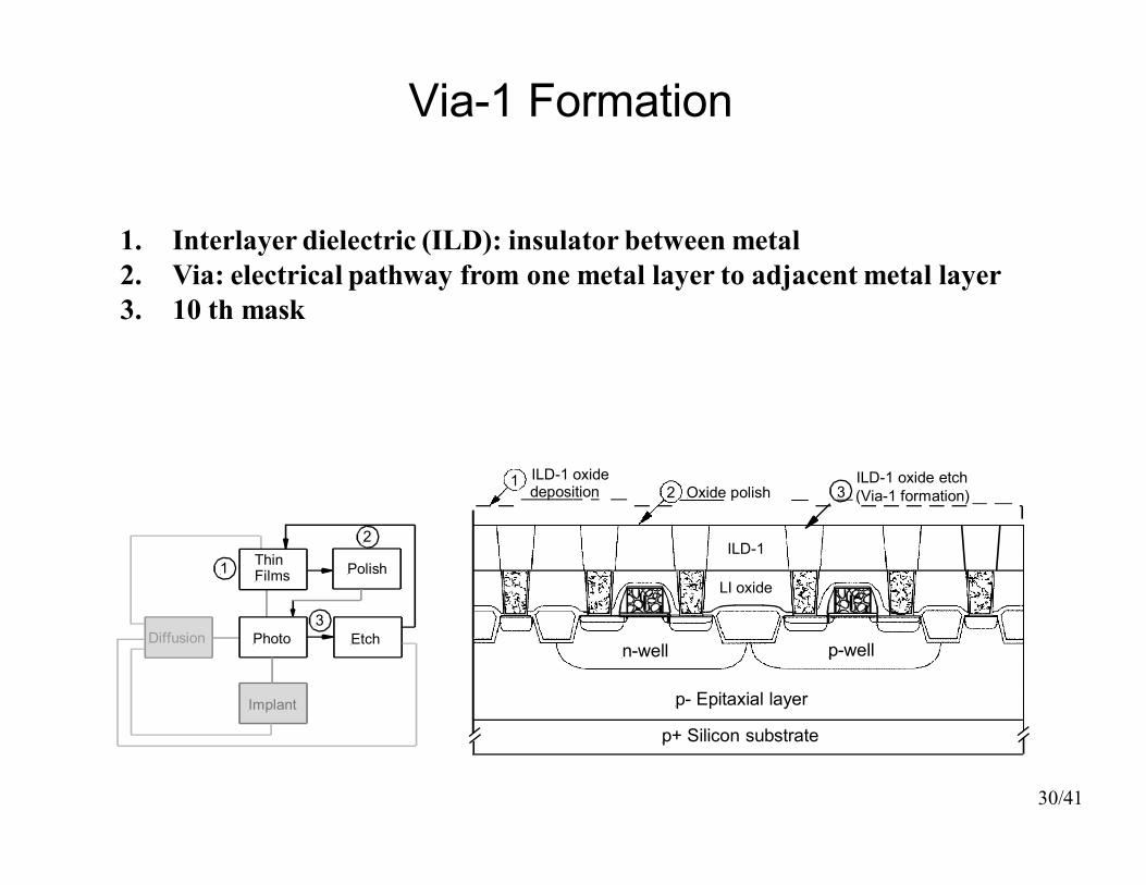
Via-1 Formation
Diffusion EtchPhoto
Implant
Polish
3
2
1 ThinFilms
ILD-1 oxidedepositi
1
1. Interlayer dielectric (ILD): insulator between metal2. Via: electrical pathway from one metal layer to adjacent metal l3. 10 th mask
Formation
2 Oxide polishILD-1 oxide etch
3 (Via-1 formation)
LI oxide
oxidesition
ILD-1
p-welln-well
p- Epitaxial layer
p+ Silicon substrate
30/41
Interlayer dielectric (ILD): insulator between metalone metal layer to adjacent metal layer
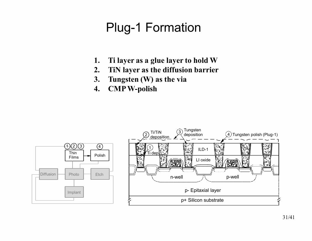
Plug-1 Formation
Thin Films
Diffusion Photo
Implant
1 2 3 4
Etch
Polish
depos2 Ti/TiN
1Ti dep.
1. Ti layer as a glue layer to hold 2. TiN layer as the3. Tungsten (W) as4. CMP W-polish
Formation
deposition 4 Tungsten polish (Plug-1)TungstendepositionTi/TiN 3
LI oxidedep.
ILD-1
p-welln-well
p- Epitaxial layer
p+ Silicon substrate
31/41
Ti layer as a glue layer to hold Wthe diffusion barrier
as the viapolish
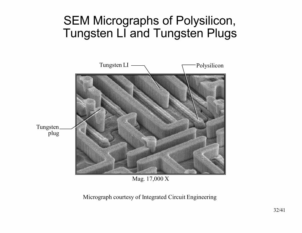
SEM Micrographs Tungsten LI and
Micrograph courtesy of Integrate
Tungsten LI
Tungstenplug
Mag. 17,000
Micrographs of Polysilicon,Tungsten Plugs
Polysilicon
Integrated Circuit Engineering
32/41
17,000 X
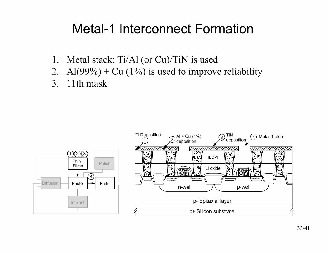
Metal-1 Interconnect
Ti Deposition1
Photo EtchDiffusion
Implant
4
1 2 3
PolishThin Films
1. Metal stack: Ti/Al (or Cu2. Al(99%) + Cu (1%) is used to improve reliability3. 11th mask
Interconnect Formation
2 3 4TiNdeposition
Al + Cu (1%)deposition
LI oxide
ILD-1
Metal-1 etch
p-welln-well
p- Epitaxial layer
p+ Silicon substrate
Cu)/TiN is usedAl(99%) + Cu (1%) is used to improve reliability
33/41
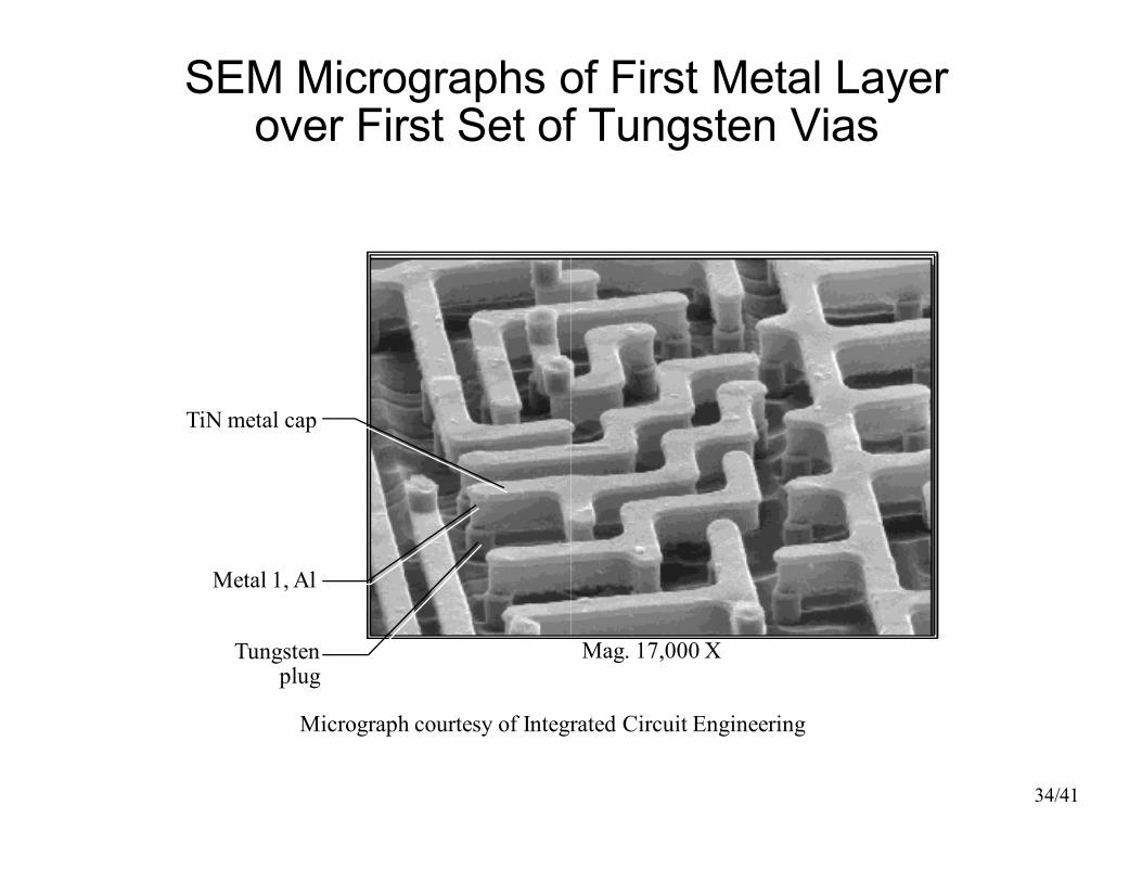
SEM Micrographs ofover First Set of
Micrograph courtesy of Integrate
TiN metal cap
Tungstenplug
Metal 1, Al
of First Metal Layerof Tungsten Vias
Integrated Circuit Engineering
Mag. 17,000 X
34/41
2 ILD-2 oxidedeposition
Photo Etch
Polish
Diffusion
Implant
4
1 2 3Thin Films
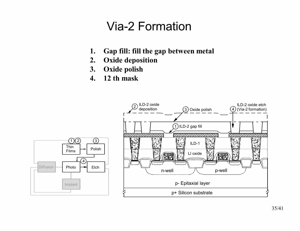
Via-2 Formation
1. Gap fill: fill the2. Oxide deposition3. Oxide polish4. 12 th mask
4
p+ Silicon substrate
p- Epitaxial layer
n-well p-well
LI oxide
ILD-1
3 Oxide polish
1 ILD-2 gap fill
oxidedeposition
ILD-2 oxide etch (Via-2 formation)
Formation
35/41
the gap between metaldeposition
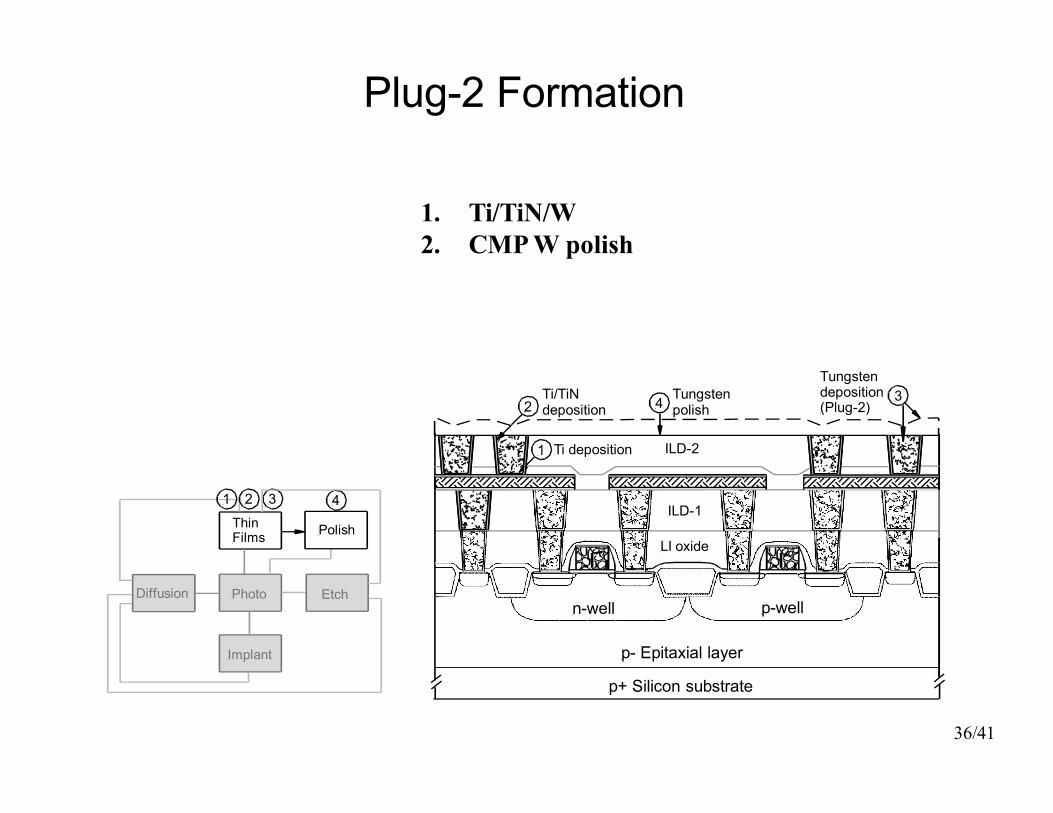
Plug-2 Formation
2
Thin Films
Diffusion Photo
Implant
1 2 3 4
Etch
Polish
1. Ti/TiN2. CMP
Formation
LI oxide
Tungstendeposition (Plug-2)
Ti/TiN deposition2
3
1 Ti deposition
ILD-1
ILD-2
p+ Silicon substrate
p- Epitaxial layer
n-well p-well
Tungstenpolish4
N/WCMP W polish
36/41
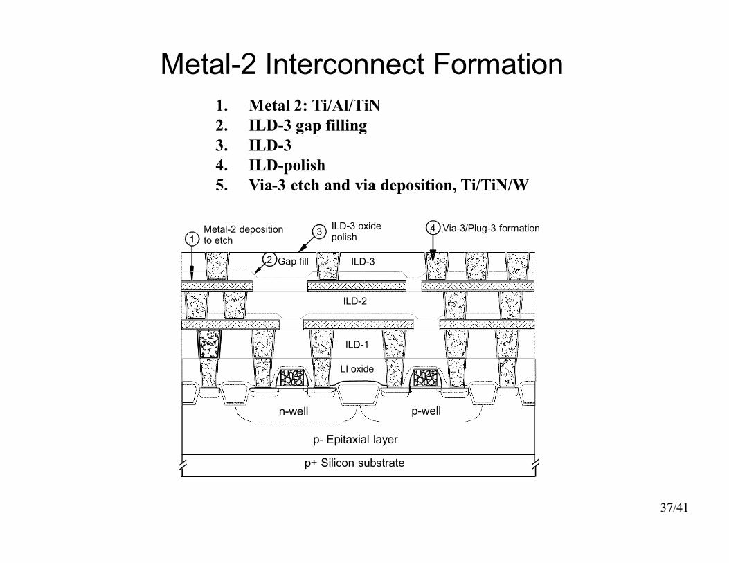
Metal-2 Interconnect
p- Epitaxial
p+ Silicon substrate
n-well
2 Gap fill
3Metal-2 deposition to etch
ILD-3 oxidepolish1
ILD-1
LI oxide
ILD-2
ILD
1. Metal 2: Ti/Al/TiN2. ILD-3 gap filling3. ILD-34. ILD-polish5. Via-3 etch and vi
Interconnect Formation
Epitaxial layer
substrate
p-well
4 Via-3/Plug-3 formationoxide
1
oxide
2
ILD-3
37/41
Ti/Al/TiNfilling
via deposition, Ti/TiN/W
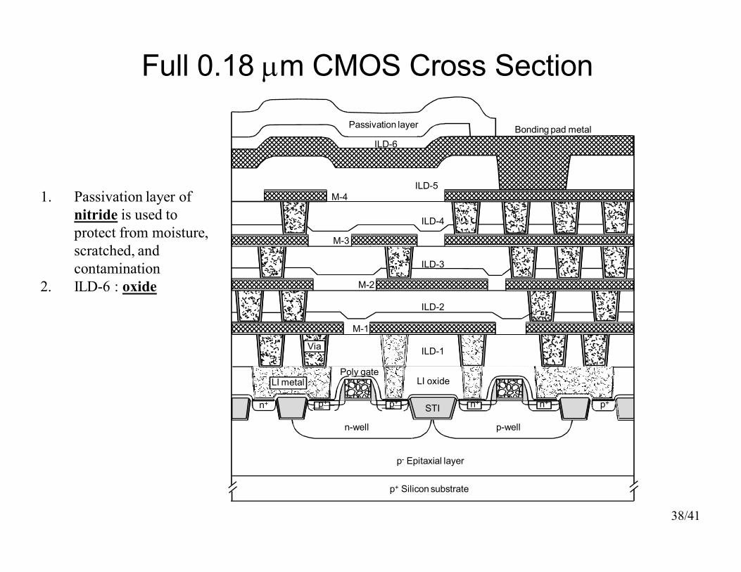
Full 0.18 m CMOS
Passivatio
n-well
M-1
M-2
M-3
M-4
Poly ga
n+
LI metal
Via
p+
1. Passivation layer of nitride is used to protect from moisture, scratched, and contamination
2. ILD-6 : oxide
CMOS Cross Section
Passivation layer Bonding pad metal
p+ Silicon substrate
LI oxide
STI
p-well
ILD-1
ILD-2
ILD-3
ILD-4
ILD-5
2
gate
p- Epitaxial layer
p+
ILD-6
38/41
p+ n+n+
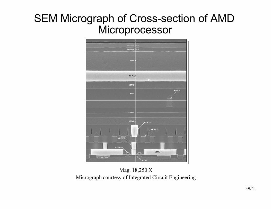
SEM Micrograph of CrossMicroprocessor
Mag. 18,250Micrograph courtesy of Integrate
Cross-section of AMDMicroprocessor
18,250 XIntegrated Circuit Engineering
39/41
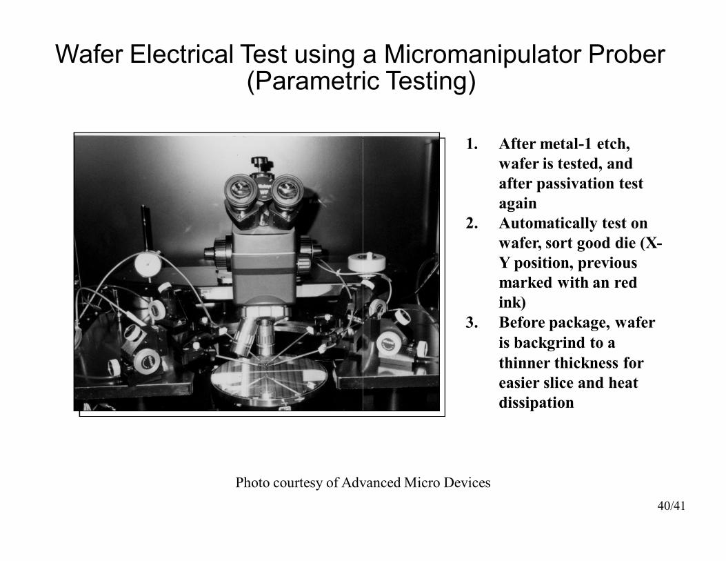
Wafer Electrical Test using a(Parametri
Photo courtesy of Advance
a Micromanipulator Prober (Parametric Testing)
Advanced Micro Devices40/41
1. After metal-1 etch, wafer is tested, and after passivation test again
2. Automatically test on wafer, sort good die (X-Y position, previous marked with an red ink)
3. Before package, wafer is backgrind to athinner thickness foreasier slice and heat dissipation