
SEEWG'05 Technology Insertion
28
NASA Tech Insertion_Sunderland_v1 1 Reliable Semiconductor Technology Insertion NASA Electronic Parts & Packaging (NEPP) Program New Technologies and Insertion into Flight Programs Workshop 30 January – 1 February 2007 David A. Sunderland, Ph.D. Boeing Satellite Development Center (SDC) El Segundo, CA [email protected] Author Author
Transcript of SEEWG'05 Technology Insertion

NASA Tech Insertion_Sunderland_v1
1
Reliable Semiconductor Technology Insertion
NASA Electronic Parts & Packaging (NEPP) Program
New Technologies and Insertion into Flight Programs Workshop
30 January – 1 February 2007
David A. Sunderland, Ph.D.Boeing Satellite Development Center (SDC)
El Segundo, [email protected]
AuthorAuthor

NASA Tech Insertion_Sunderland_v1
2
OutlineMotivationBoeing SDC Technology Insertion ProcessSemiconductor Qualification Issues
● Generic● Process, Product, Packaging and Lot
Wearout Life and Failure RateProgrammable Device IssuesMisconceptions and PitfallsCase Study
● Insertion of Advanced IBM ASIC Technology
Conclusions

NASA Tech Insertion_Sunderland_v1
3
MotivationSatellite payload performance targets continually increase, yet constraints do not relax (often they worsen)
● Size, weight and power● Environmental hazards (e.g. temperature, radiation)● Long-life reliability requirements● Schedule pressure● Risk aversion
Achieving these targets requires access to advanced semiconductor technologies
● Beyond capabilities of classical “hi-rel” fabs● Along with improved performance, advanced commercial-driven
technologies bring more advanced I/P and design toolsSuccessful insertion of “bleeding edge” technology requires:
● Extensive knowledge of failure mechanisms● Insight to design around technology limitations ● Robust screening flow

NASA Tech Insertion_Sunderland_v1
4
Boeing SDC Technology Insertion ProcessProposed Process Flowchart
In each phase of Technology Insertion (Fund, Bid, Baseline, Change and Qualification), we iterate these steps: ● Development Plan● Maturity Assessment ● Approval (by non-advocate review team)
IR&D Phase Program Execution PhaseBid Phase
Ready to BidReady to Bid
Ready to BaselineReady to Baseline
Baseline ChangeBaseline Change
Qualification ReviewQualification Review
T1T1T1Develop Strategy
Develop Strategy
T2T2T2Develop TechnologyDevelop
Technology
Ready to FundReady to Fund
T3T3T3Plan Insertion
Plan Insertion
T4T4T4
T5T5T5

NASA Tech Insertion_Sunderland_v1
5
Boeing SDC Technology Insertion ProcessKey Attributes
SDC’s Technology Insertion Process (TIP) is evolving to meet advanced technology needs● Local process tailored to advanced semiconductor
technologies is consistent with Enterprise directions● Builds on Product Qualification framework of Boeing PRO-0219
Standardized Qualification Statements Of Work (QSOWs) cover product level test requirementsNASA Technology Readiness Level (TRL) scale used as guide in Maturity Assessment ● “Necessary” (expected by customers) but not “sufficient” to
ensure a reliable insertion● Specialized checklists (e.g. for custom semiconductor devices)
aid in probing deeperSDC rolling out new “Device Qualification” training course to help Component Engineers and technology users understand intricacies

NASA Tech Insertion_Sunderland_v1
6
Semiconductor Qualification IssuesWhat is Qualification?
Generic definitions● To collect data, from the supplier or by experiment,
sufficient to demonstrate to ourselves and our customers that a technology is suitable for our applications
● Qualification validates that the design and processes utilized are such that the product will meet all of its worst-case requirements for a period well beyond mission life
Given these definitions, we believe qualification of semiconductor products should be a hierarchical process, including review of:
● Semiconductor process● Primitive device elements● Libraries● Chip design● Package● Delivered lots
Industry standard component qualifications seldom go this deep

NASA Tech Insertion_Sunderland_v1
7
Semiconductor Qualification IssuesProcess
Process, library, design infrastructure maturity● Required elements demonstrated in silicon?
Model-to-hardware correlationQuality systemStatistical process controlDevice wearout (active, passive and interconnect)
● Dominant failure mechanisms● Time-to-failure distributions ● Acceleration factors and models
Random failure rate vs. complexityScreening flow Device level radiation effectsEnvironmental sensitivity (e.g. hydrogen, moisture)

NASA Tech Insertion_Sunderland_v1
8
Semiconductor Qualification IssuesProduct
Compliance with design guidelines
Performance over use environment (process, temperature, voltage)
Circuit level radiation effects● Single Event Upset (SEU) rates & mitigation
Wearout under use conditions vs. design life
Overstress effects
Random failure rate modeling
Failure Mode Effects Analysis (FMEA)
ESD threshold levels

NASA Tech Insertion_Sunderland_v1
9
Semiconductor Qualification IssuesPackaging
Vacuum● Materials must not out-gas
Radiation● Materials must not degrade
Vibration (low frequency) and shock (high frequency) resistance
● Launch and pyro-shock events associated with spacecraft deployments
Humidity (for non-hermetic packages)● Moisture (introduced on the ground) must not cause
corrosion or expansionCoefficient of thermal expansion (CTE)
● A poor match to board stresses connectionsThermal impedance
● No airflow; heat must be extracted by conduction onlyDissimilar metals

NASA Tech Insertion_Sunderland_v1
10
Semiconductor Qualification IssuesLot
Industry standard Quality Conformance Inspection (QCI) and Lot Acceptance Test (LAT) methods focus on “qualifying” specific delivered lots
● Validate that “signature” of a given lot of devices is similar or in compliance with process and product qualification “signatures”
Typically includes High Temperature Operating Life (HTOL), temp cycling, thermal shock, vibration/shock/acceleration
● Often same tests employed in screening, but at higher levels or longer time frames
Includes Radiation Lot Acceptance Test (RLAT) unless large margin established in process and product qualification

NASA Tech Insertion_Sunderland_v1
11
Wearout Life and Failure RateBathtub Curve
“Intrinsic” failures are those of “normal” population of primitive device elements (active and passive devices, contacts and wires)●Since they are nearly uniform, they tend to wear out closely in time
given fixed stress●Results in the “wearout” region of bathtub curve (Weibull slope > 1)
“Extrinsic” failures are (early) wearout of abnormal or defective device elements (e.g. thin oxide or narrow metal spots)●Such elements are present in any large population●Results in “infant mortality” region of bathtub curve (Weibull slope < 1)
Useful Life
Wear outConstant failure rateInfant Mortality
Time (t)
I/MTBF
Failure rate = f(t)
0

NASA Tech Insertion_Sunderland_v1
12
Wearout Life and Failure RateWhat Leads to a “Reliable” Device?
Circuit stress should be controlled (by design) so that rate of intrinsic fails is negligible (e.g. <10% of total failure rate) during “design life”
● Margin between MTTF and design life must be sufficient (e.g. 3-10x) to allow for statistical variation in time to failure
● This is particularly important for devices with millions of elements
When this is done, net failure rate is determined by extrinsic fails (“random failure rate”)
● Tighter screens mean lower defect density, hence lower failure rate
● To be effective, screens must focus on dominant defect mechanisms (“Pareto”)
● This failure rate scales with complexity of product

NASA Tech Insertion_Sunderland_v1
13
Programmable DevicesSpecial Issues
Device elements like these require special handling in qualification ● Floating gate MOSFETs● Phase-change memory● Fuses (laser and electrically programmed)● Antifuses● Trimmed resistors
They have multiple configurations that must remain stable and distinct● That much more challenging if element state is “analog”
They are typically programmed by stress that would not be allowable in “normal” devices
● There may be little margin between programming and wearout● Programming stress must be limited to desired elements
Programming often depends on initiation at natural defect site● Leads to extra variability – every device is slightly different (and there may
be LOTS of them on every chip)● Special feedback circuits or programming algorithms allow for “trimming”
result to get reasonable statistics

NASA Tech Insertion_Sunderland_v1
14
Programmable DevicesSome Things to Look for in QualificationProgramming/erase physical mechanisms Programming/erase circuits and algorithmsProgrammed/un-programmed state statisticsRetention time statisticsModels for retention time vs. temperature
● Basis for modeling parametersIf multiple program/erase cycles are allowed, endurance statistics
● Effect of program/erase cycles on retentionRadiation effects on programmed state, endurance and retentionWearout statistics for programmable elements, e.g.:
● TDDB, HCI for floating gate MOSFETs● TDDB for un-programmed, EM for programmed antifuses
Corrosion resistance for laser-programmed fuses

NASA Tech Insertion_Sunderland_v1
15
Misconceptions and PitfallsWearout Life
MTTF is insufficient to determine when “tail” devices fail● Shape of failure distribution is critical
Failure to consider all device types (active, passive & interconnect) that make up the chip
● Each has multiple unique failure mechanisms● All are not accelerated in the same way
Temperature is often only accelerating factor considered● Others include voltage, current, frequency, duty cycle, over/under-
shoot and thermal cyclingFailure mechanisms that dominate under burn-in conditions may not dominate in use
● e.g. low EA thermal mechanismsMoore’s Law trends are reducing wearout life margin
● Designing long-life products is still possible, but requires more analysis and use condition (e.g. T, V, f) derating

NASA Tech Insertion_Sunderland_v1
16
Misconceptions and PitfallsFailure Rate
Depending on lot sample burn-in (e.g. 77 parts, 1000 hours, 125°C) to determine failure rate
● This can only estimate gross upper bound to failure rate to determine if lot is “in family”
● Measuring failure rate requires larger sample size and accelerationExpectations based on “bathtub curve” may be unrealistic
● “Infant mortality” (decreasing failure rate with time) likely extends throughout useful life
● A “good” screening flow minimizes infant mortality by reducing defect density – it doesn’t eliminate it
Acceleration factors (e.g. EA for temperature) are often assumed rather than modeled
● Carry-over from “similar” processes may not be valid“Hi-rel” parts are not necessarily more reliable than “commercial” parts
● Niche fabs exhibit much higher defect density

NASA Tech Insertion_Sunderland_v1
17
Misconceptions and PitfallsMaturity Assessment
DSCC certification is not enough● Focuses on lot qualification
Peer review of vendor data is often inadequate● Proprietary issues make proper review difficult
● Managing subcontractor’s Technology Insertion is even harder
Prior qualification or even flight does not mean we are “done”
● Environment or use conditions may have changed
● Previous qualification may have missed something
● Process or product may have changed

NASA Tech Insertion_Sunderland_v1
18
Case StudyIBM ASIC Technology Insertion
To illustrate, this section reviews Boeing’s space insertion of two generations of IBM ASIC technology
For more detail, see:●Sunderland, et al., “Megagate ASICs for the Thuraya Satellite Digital
Signal Processor”, IEEE Intl. Symp. on Quality Electronic Design, 3/2002
●Sunderland, et al., “Second Generation Megagate ASICs for the SPACEWAYTM Satellite Communications Payload”, NASA Symp. on VLSI Design, 5/2003
For reports on other recent technology insertions, see:●Rosenthal, et al., “Acceleration Parameters and Reliability of SiGe
HBTs During Long-Term Forward-Biased Operation”, IEEE/JEDEC Reliability of Compound Semiconductors Workshop, 10/2004
●Delaney and Paine, “Qualification of Commercial and Custom Semiconductor Processes for Spaceborne Applications”, NRO Conf. on Communications Technology, 2002

NASA Tech Insertion_Sunderland_v1
19
IBM ASIC Technology InsertionTechnologies
First Generation ●Qualified 6/1998, on orbit since 10/2000●SA-12 ASIC process and library
– 0.25µm-gate, Al metal, 2.5V– Used for ASICs up to 2.9Mgate
●Ceramic Column Grid Array (CCGA) packaging
Second Generation●Qualified 8/1999, on orbit since 12/2003●SA-27 ASIC process and library
– 0.16µm-gate, Cu metal, 1.8V– Used for ASICs up to 5.1Mgate

NASA Tech Insertion_Sunderland_v1
20
IBM ASIC Technology InsertionCCGA Overview
Offers high lead count in a given area● 1088 lead, 42x42mm, 1.27mm pitch version used for SPACEWAY
Non-hermetic but “level 1” moisture resistant High reliability flip-chip die-to-substrate interface● Low package CTE (6.5 ppm/°C); die is epoxy underfilled
High thermal cycle fatigue life ● 10x that of same size
Ceramic Ball Grid Array ● Flexible, tall columns
take strain off PWB interface
NASA Tech Insertion_Sunderland_v1
21
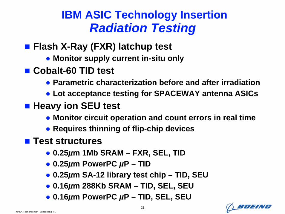
IBM ASIC Technology InsertionRadiation Testing
Flash X-Ray (FXR) latchup test● Monitor supply current in-situ only
Cobalt-60 TID test● Parametric characterization before and after irradiation● Lot acceptance testing for SPACEWAY antenna ASICs
Heavy ion SEU test● Monitor circuit operation and count errors in real time● Requires thinning of flip-chip devices
Test structures● 0.25µm 1Mb SRAM – FXR, SEL, TID● 0.25µm PowerPC µP – TID● 0.25µm SA-12 library test chip – TID, SEU● 0.16µm 288Kb SRAM – TID, SEL, SEU ● 0.16µm PowerPC µP – TID, SEL, SEU

NASA Tech Insertion_Sunderland_v1
22
IBM ASIC Technology InsertionRadiation Test Results
Total Ionizing Dose (TID)● Thinner gate oxide leads to improved radiation tolerance
● Largest effect is increased quiescent supply current from field oxide charging
Single-Event Latchup (SEL)● These IBM processes are immune by design (Vhold > VDD)
● No latchup or permanent errors seen up to most energetic particles used
Single-Event Upset (SEU)● Rate is low enough rate to handle with circuit redundancy
Results are short of “radiation hard” definitions, but are adequate to meet most program requirements
NASA Tech Insertion_Sunderland_v1
23
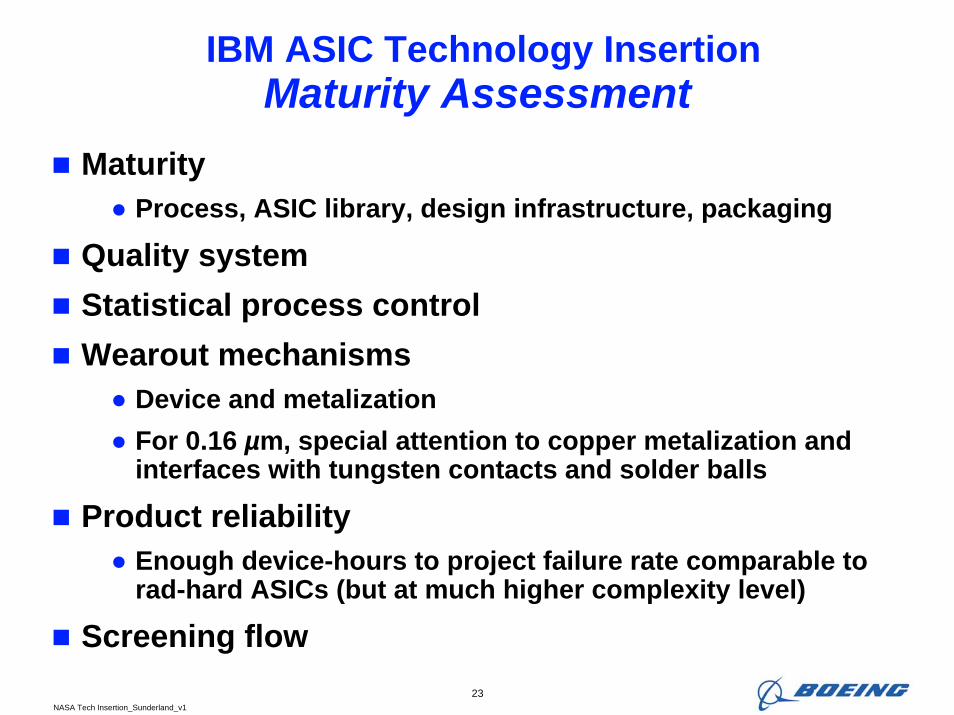
IBM ASIC Technology InsertionMaturity Assessment
Maturity● Process, ASIC library, design infrastructure, packaging
Quality systemStatistical process controlWearout mechanisms
● Device and metalization● For 0.16 µm, special attention to copper metalization and
interfaces with tungsten contacts and solder balls
Product reliability● Enough device-hours to project failure rate comparable to
rad-hard ASICs (but at much higher complexity level)
Screening flow

NASA Tech Insertion_Sunderland_v1
24
IBM ASIC Technology InsertionWearout Life, Screening and Failure Rate
IBM’s design rules written to avoid occurrence of wearout during product lifetime (typically ≥100Khr)
● Verified as part of process qualification
● Longer service life required analysis of use conditions against modeled hot carrier and electro-migration lifetime
IBM’s “Grade 1” screens (developed for mainframes) reduce fail rate target 10x over commercial product
● Result is a product which exceeds the reliability of MIL-STD-883 Class S components
● Boeing added an enhanced IDDQ screen to better spot “out of family” devices with limited sample size

NASA Tech Insertion_Sunderland_v1
25
IBM ASIC Technology InsertionCCGA Package Qualification
IBM qualification data extensively reviewed● Data supportive of application, but needed supplement
Underfill material passed vacuum out-gassing testVacuum thermal model developed, verified by test
● Temperature rise at junction meets reliability targets
Accelerated vibration, shock and thermal cycle tests● 72 samples built into PWBs by Boeing and IBM ● 32 & 42mm packages, daisy chain wiring, no die● 70,000 connections continuously monitored● Tests show sufficient margin to program requirements
Robust assembly and rework processes developed for Boeing manufacturing flow using IBM guidelines

NASA Tech Insertion_Sunderland_v1
26
IBM ASIC Technology InsertionPerformance
Table compares DSP units for SPACEWAY, THURAYA and ICO ● ICO uses traditional 0.7µm rad-hard ASICs and wirebond MCMs
At 62 trillion operations per second (TOPS), SPACEWAY contains the world’s most powerful satellite-based DSP
●10,000 Pentium III-based computers to do same function in software4x throughput increase ICO →THURAYA with 8x fewer ASICs
●Reducing 4 units to 2 saved 30% in weight, 20% in volume●Power approximately constant with much more function
4x throughput increase THURAYA → SPACEWAY ●Reducing 2 units to 1 saved 35% in weight, 50% in volume
Parameter ICO THURAYA SPACEWAY Capability (TOPS) 3.6 14 62 ASICs 2300 360 390 MCMs 300 eliminated eliminated Units 4 2 1 Volume (m3) 0.34 0.28 0.13 Weight (kg) 270 190 124 Power (W) 2200 2300 2100

NASA Tech Insertion_Sunderland_v1
27
ConclusionsThe advanced semiconductor technologies needed to meet increasing satellite performance targets within fixed resource constraints require great insight in technology insertionBoeing has developed a tailored semiconductor Technology Insertion Process that effectively manages the more extensive maturity assessment reviews this insight impliesReliable technology insertion requires a hierarchical approach, looking at a wealth of process, product, packaging and lot specific issuesIntrinsic wearout life, with statistical margin, must exceed design life, so that defect-driven failure rate dominates and can be reduced by focused screensProgrammable devices have unique issues that require special attention in process and product qualificationThere are numerous opportunities to trip upBoeing’s space insertion of IBM ASIC technology provides an excellent example of the discipline required
NASA Tech Insertion_Sunderland_v1
28
AcknowledgmentsThe author gratefully acknowledges the assistance of the following individuals
● Martin Drake● Jim Hall● Andrew King● Bruce Paine● Len Rosenheck● Bill Rowe● Gary Warren● Steve Wharfield


