SECTION 9 HARDWARE DESIGN TECHNIQUES - Spread · PDF file · 1997-08-012 SECTION 9...
92
1 SECTION 9 HARDWARE DESIGN TECHNIQUES Prototyping Analog Circuits Evaluation Boards Noise Reduction and Filtering for Switching Power Supplies Low Dropout References and Regulators EMI/RFI Considerations Sensors and Cable Shielding
-
Upload
phamnguyet -
Category
Documents
-
view
225 -
download
1
Transcript of SECTION 9 HARDWARE DESIGN TECHNIQUES - Spread · PDF file · 1997-08-012 SECTION 9...
1
SECTION 9
HARDWARE DESIGN TECHNIQUES
Prototyping Analog Circuits
Evaluation Boards
Noise Reduction and Filtering forSwitching Power Supplies
Low Dropout References and Regulators
EMI/RFI Considerations
Sensors and Cable Shielding
2
SECTION 9
HARDWARE DESIGN TECHNIQUESWalt Kester, James Bryant, Walt Jung,Adolfo Garcia, John McDonald
PROTOTYPING AND SIMULATING ANALOG CIRCUITSWalt Kester, James Bryant
While there is no doubt that computer analysis is one of the most valuable tools thatthe analog designer has acquired in the last decade or so, there is equally no doubtthat analog circuit models are not perfect and must be verified with hardware. If theinitial test circuit or "breadboard" is not correctly constructed, it may suffer frommalfunctions which are not the fault of the design but of the physical structure ofthe breadboard itself. This section considers the art of successful breadboarding ofhigh performance analog circuits.
Real electronic circuits contain many "components" which were not present in thecircuit diagram, but which are there because of the physical properties ofconductors, circuit boards, IC packages, etc. These components are difficult, if notimpossible, to incorporate into computer modeling software, and yet they havesubstantial effects on circuit performance at high resolutions, or high frequencies, orboth.
It is therefore inadvisable to use SPICE modeling or similar software to predict theultimate performance of such high performance analog circuits. After modeling iscomplete, the performance must be verified by experiment.
This is not to say that SPICE modeling is valueless - far from it. Most modern highperformance analog circuits could never have been developed without the aid ofSPICE and similar programs, but it must be remembered that such simulations areonly as good as the models used, and these models are not perfect. We have seen theeffects of parasitic components arising from the conductors, insulators andcomponents on the PCB, but it is also necessary to appreciate that the models usedwithin SPICE simulations are not perfect models.
Consider an operational amplifier. It contains some 20-40 transistors, almost asmany resistors, and a few capacitors. A complete SPICE model will contain all thesecomponents, and probably a few of the more important parasitic capacitances andspurious diodes formed by the diffusions in the op-amp chip. This is the model thatthe designer will have used to evaluate the device during his design. In simulations,such a model will behave very like the actual op-amp, but not exactly.
3
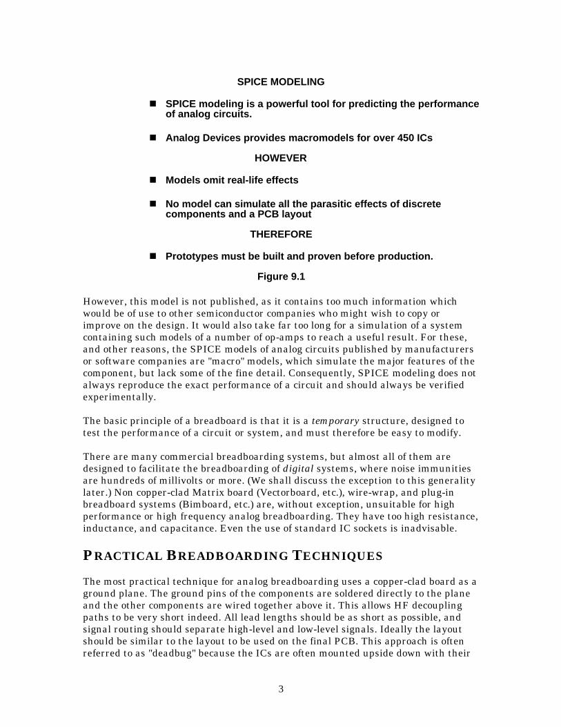
SPICE MODELING
SPICE modeling is a powerful tool for predicting the performanceof analog circuits.
Analog Devices provides macromodels for over 450 ICs
HOWEVER
Models omit real-life effects
No model can simulate all the parasitic effects of discretecomponents and a PCB layout
THEREFORE
Prototypes must be built and proven before production.
Figure 9.1
However, this model is not published, as it contains too much information whichwould be of use to other semiconductor companies who might wish to copy orimprove on the design. It would also take far too long for a simulation of a systemcontaining such models of a number of op-amps to reach a useful result. For these,and other reasons, the SPICE models of analog circuits published by manufacturersor software companies are "macro" models, which simulate the major features of thecomponent, but lack some of the fine detail. Consequently, SPICE modeling does notalways reproduce the exact performance of a circuit and should always be verifiedexperimentally.
The basic principle of a breadboard is that it is a temporary structure, designed totest the performance of a circuit or system, and must therefore be easy to modify.
There are many commercial breadboarding systems, but almost all of them aredesigned to facilitate the breadboarding of digital systems, where noise immunitiesare hundreds of millivolts or more. (We shall discuss the exception to this generalitylater.) Non copper-clad Matrix board (Vectorboard, etc.), wire-wrap, and plug-inbreadboard systems (Bimboard, etc.) are, without exception, unsuitable for highperformance or high frequency analog breadboarding. They have too high resistance,inductance, and capacitance. Even the use of standard IC sockets is inadvisable.
PRACTICAL BREADBOARDING TECHNIQUES
The most practical technique for analog breadboarding uses a copper-clad board as aground plane. The ground pins of the components are soldered directly to the planeand the other components are wired together above it. This allows HF decouplingpaths to be very short indeed. All lead lengths should be as short as possible, andsignal routing should separate high-level and low-level signals. Ideally the layoutshould be similar to the layout to be used on the final PCB. This approach is oftenreferred to as "deadbug" because the ICs are often mounted upside down with their
4
leads up in the air (with the exception of the ground pins, which are bent over andsoldered directly to the ground plane). The upside-down ICs look liked deceasedinsects, hence the name.
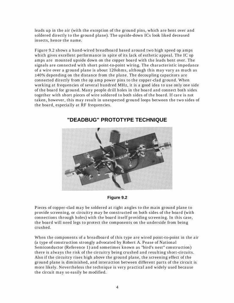
Figure 9.2 shows a hand-wired breadboard based around two high speed op ampswhich gives excellent performance in spite of its lack of esthetic appeal. The IC opamps are mounted upside down on the copper board with the leads bent over. Thesignals are connected with short point-to-point wiring. The characteristic impedanceof a wire over a ground plane is about 120ohms, although this may vary as much as±40% depending on the distance from the plane. The decoupling capacitors areconnected directly from the op amp power pins to the copper-clad ground. Whenworking at frequencies of several hundred MHz, it is a good idea to use only one sideof the board for ground. Many people drill holes in the board and connect both sidestogether with short pieces of wire soldered to both sides of the board. If care is nottaken, however, this may result in unexpected ground loops between the two sides ofthe board, especially at RF frequencies.
"DEADBUG" PROTOTYPE TECHNIQUE
Figure 9.2
Pieces of copper-clad may be soldered at right angles to the main ground plane toprovide screening, or circuitry may be constructed on both sides of the board (withconnections through holes) with the board itself providing screening. In this case,the board will need legs to protect the components on the underside from beingcrushed.
When the components of a breadboard of this type are wired point-to-point in the air(a type of construction strongly advocated by Robert A. Pease of NationalSemiconductor (Reference 1) and sometimes known as "bird's nest" construction)there is always the risk of the circuitry being crushed and resulting short-circuits.Also if the circuitry rises high above the ground plane, the screening effect of theground plane is diminished, and interaction between different parts of the circuit ismore likely. Nevertheless the technique is very practical and widely used becausethe circuit may so easily be modified.
5
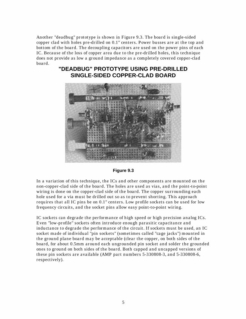
Another "deadbug" prototype is shown in Figure 9.3. The board is single-sidedcopper clad with holes pre-drilled on 0.1" centers. Power busses are at the top andbottom of the board. The decoupling capacitors are used on the power pins of eachIC. Because of the loss of copper area due to the pre-drilled holes, this techniquedoes not provide as low a ground impedance as a completely covered copper-cladboard.
"DEADBUG" PROTOTYPE USING PRE-DRILLEDSINGLE-SIDED COPPER-CLAD BOARD
Figure 9.3
In a variation of this technique, the ICs and other components are mounted on thenon-copper-clad side of the board. The holes are used as vias, and the point-to-pointwiring is done on the copper-clad side of the board. The copper surrounding eachhole used for a via must be drilled out so as to prevent shorting. This approachrequires that all IC pins be on 0.1" centers. Low profile sockets can be used for lowfrequency circuits, and the socket pins allow easy point-to-point wiring.
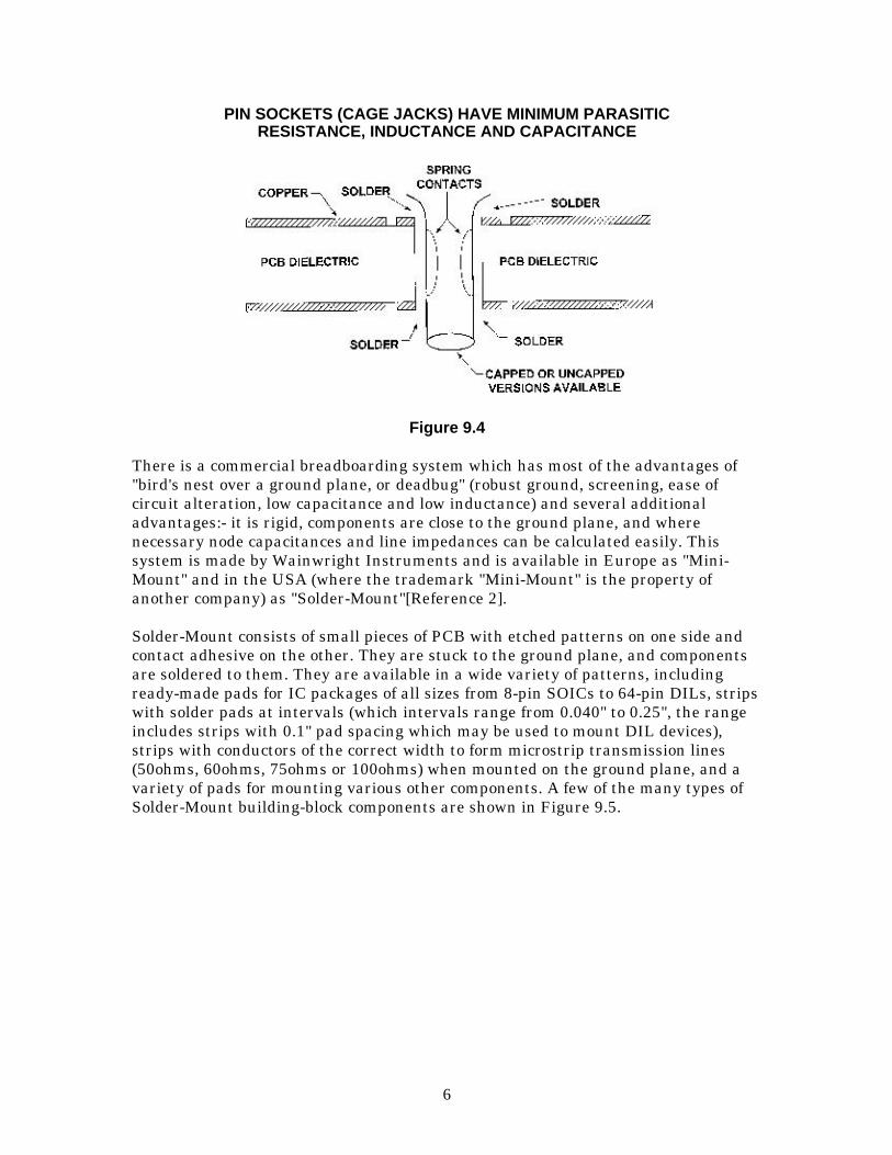
IC sockets can degrade the performance of high speed or high precision analog ICs.Even "low-profile" sockets often introduce enough parasitic capacitance andinductance to degrade the performance of the circuit. If sockets must be used, an ICsocket made of individual "pin sockets" (sometimes called "cage jacks") mounted inthe ground plane board may be acceptable (clear the copper, on both sides of theboard, for about 0.5mm around each ungrounded pin socket and solder the groundedones to ground on both sides of the board. Both capped and uncapped versions ofthese pin sockets are available (AMP part numbers 5-330808-3, and 5-330808-6,respectively).
6
PIN SOCKETS (CAGE JACKS) HAVE MINIMUM PARASITICRESISTANCE, INDUCTANCE AND CAPACITANCE
Figure 9.4
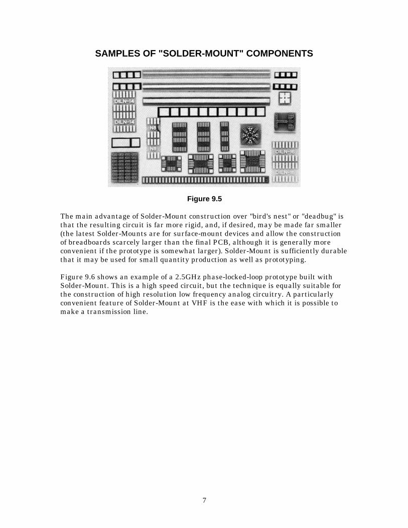
There is a commercial breadboarding system which has most of the advantages of"bird's nest over a ground plane, or deadbug" (robust ground, screening, ease ofcircuit alteration, low capacitance and low inductance) and several additionaladvantages:- it is rigid, components are close to the ground plane, and wherenecessary node capacitances and line impedances can be calculated easily. Thissystem is made by Wainwright Instruments and is available in Europe as "Mini-Mount" and in the USA (where the trademark "Mini-Mount" is the property ofanother company) as "Solder-Mount"[Reference 2].
Solder-Mount consists of small pieces of PCB with etched patterns on one side andcontact adhesive on the other. They are stuck to the ground plane, and componentsare soldered to them. They are available in a wide variety of patterns, includingready-made pads for IC packages of all sizes from 8-pin SOICs to 64-pin DILs, stripswith solder pads at intervals (which intervals range from 0.040" to 0.25", the rangeincludes strips with 0.1" pad spacing which may be used to mount DIL devices),strips with conductors of the correct width to form microstrip transmission lines(50ohms, 60ohms, 75ohms or 100ohms) when mounted on the ground plane, and avariety of pads for mounting various other components. A few of the many types ofSolder-Mount building-block components are shown in Figure 9.5.
7
SAMPLES OF "SOLDER-MOUNT" COMPONENTS
Figure 9.5
The main advantage of Solder-Mount construction over "bird's nest" or "deadbug" isthat the resulting circuit is far more rigid, and, if desired, may be made far smaller(the latest Solder-Mounts are for surface-mount devices and allow the constructionof breadboards scarcely larger than the final PCB, although it is generally moreconvenient if the prototype is somewhat larger). Solder-Mount is sufficiently durablethat it may be used for small quantity production as well as prototyping.
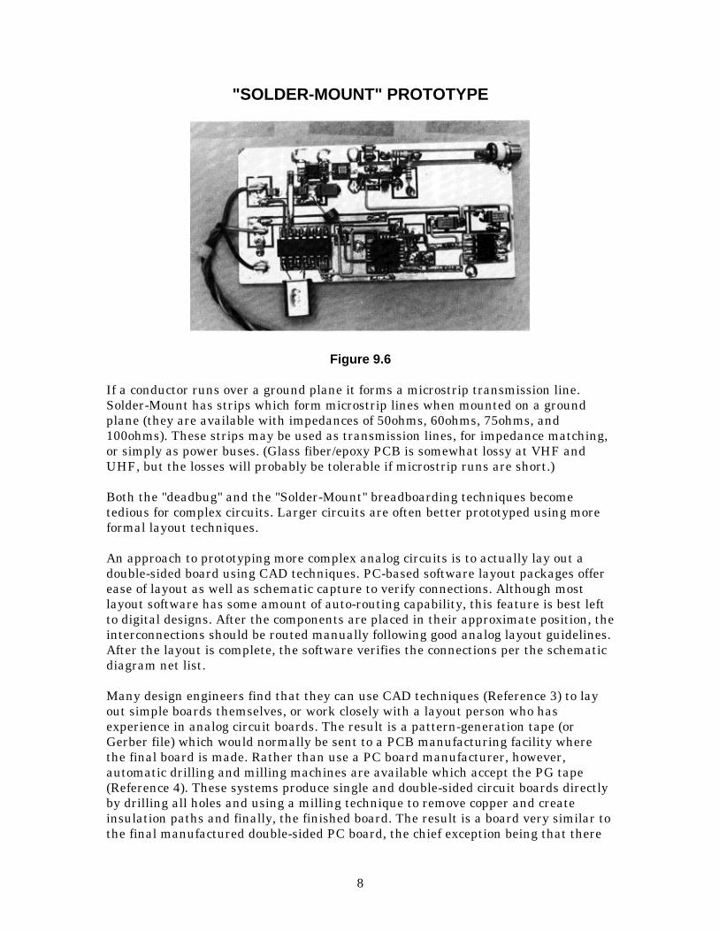
Figure 9.6 shows an example of a 2.5GHz phase-locked-loop prototype built withSolder-Mount. This is a high speed circuit, but the technique is equally suitable forthe construction of high resolution low frequency analog circuitry. A particularlyconvenient feature of Solder-Mount at VHF is the ease with which it is possible tomake a transmission line.
8
"SOLDER-MOUNT" PROTOTYPE
Figure 9.6
If a conductor runs over a ground plane it forms a microstrip transmission line.Solder-Mount has strips which form microstrip lines when mounted on a groundplane (they are available with impedances of 50ohms, 60ohms, 75ohms, and100ohms). These strips may be used as transmission lines, for impedance matching,or simply as power buses. (Glass fiber/epoxy PCB is somewhat lossy at VHF andUHF, but the losses will probably be tolerable if microstrip runs are short.)
Both the "deadbug" and the "Solder-Mount" breadboarding techniques becometedious for complex circuits. Larger circuits are often better prototyped using moreformal layout techniques.
An approach to prototyping more complex analog circuits is to actually lay out adouble-sided board using CAD techniques. PC-based software layout packages offerease of layout as well as schematic capture to verify connections. Although mostlayout software has some amount of auto-routing capability, this feature is best leftto digital designs. After the components are placed in their approximate position, theinterconnections should be routed manually following good analog layout guidelines.After the layout is complete, the software verifies the connections per the schematicdiagram net list.
Many design engineers find that they can use CAD techniques (Reference 3) to layout simple boards themselves, or work closely with a layout person who hasexperience in analog circuit boards. The result is a pattern-generation tape (orGerber file) which would normally be sent to a PCB manufacturing facility wherethe final board is made. Rather than use a PC board manufacturer, however,automatic drilling and milling machines are available which accept the PG tape(Reference 4). These systems produce single and double-sided circuit boards directlyby drilling all holes and using a milling technique to remove copper and createinsulation paths and finally, the finished board. The result is a board very similar tothe final manufactured double-sided PC board, the chief exception being that there
9
is no "plated-through" hole capability, and any "vias" between the two layers of theboard must be wired and soldered on both sides. Minimum trace widths of 25 mils (1mil = 0.001") and 12 mil spacing between traces are standard, although smallertrace widths can be achieved with care. The minimum spacing between lines isdictated by the size of the milling bit, typically 10 to 12 mils.
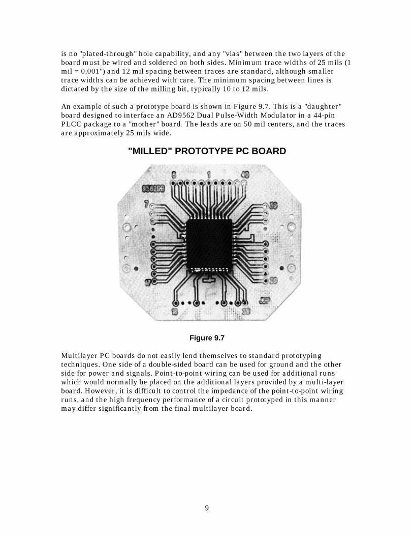
An example of such a prototype board is shown in Figure 9.7. This is a "daughter"board designed to interface an AD9562 Dual Pulse-Width Modulator in a 44-pinPLCC package to a "mother" board. The leads are on 50 mil centers, and the tracesare approximately 25 mils wide.
"MILLED" PROTOTYPE PC BOARD
Figure 9.7
Multilayer PC boards do not easily lend themselves to standard prototypingtechniques. One side of a double-sided board can be used for ground and the otherside for power and signals. Point-to-point wiring can be used for additional runswhich would normally be placed on the additional layers provided by a multi-layerboard. However, it is difficult to control the impedance of the point-to-point wiringruns, and the high frequency performance of a circuit prototyped in this mannermay differ significantly from the final multilayer board.
10
SUCCESSFUL PROTOTYPING
Always use a ground plane for precision or high frequencycircuits
Minimize parasitic resistance, capacitance, and inductance
If sockets are required, use “pin sockets” (“cage jacks”)
Pay equal attention to signal routing, component placement,grounding, and decoupling in both the prototype and the finaldesign
Popular prototyping techiniques:
Freehand “deadbug” using point-to-point wiring“Solder-Mount”Milled PC board from CAD layoutMultilayer boards: Double-sided with additional point-to-point wiring
Figure 9.8
EVALUATION BOARDS
Manufacturer's evaluation boards provide a convenient way of evaluating high-performance ICs without the need for constructing labor-intensive prototype boards.Analog Devices provides evaluation boards for almost all new high speed andprecision products. The boards are designed with good layout, grounding, anddecoupling techniques. They are completely tested, and artwork (including PG tape)is available to customers.
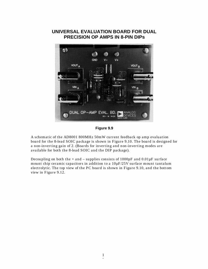
Because of the popularity of dual precision op amps in 8-pin DIPs, a universalevaluation board has been developed (see Figure 9.9). This board makes extensiveuse of pin sockets to allow resistors or jumpers to configure the two op amps in justabout any conceivable feedback, input/output, and load condition. The inputs andoutputs are convenient right-angle BNC connectors. Because of the use of socketsand the less-than-compact layout, this board is not useful for op amps having gain-bandwidth products much greater than 10MHz.
11
UNIVERSAL EVALUATION BOARD FOR DUALPRECISION OP AMPS IN 8-PIN DIPs
Figure 9.9
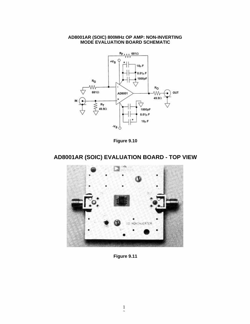
A schematic of the AD8001 800MHz 50mW current feedback op amp evaluationboard for the 8-lead SOIC package is shown in Figure 9.10. The board is designed fora non-inverting gain of 2. (Boards for inverting and non-inverting modes areavailable for both the 8-lead SOIC and the DIP package).
Decoupling on both the + and – supplies consists of 1000pF and 0.01µF surfacemount chip ceramic capacitors in addition to a 10µF/25V surface mount tantalumelectrolytic. The top view of the PC board is shown in Figure 9.10, and the bottomview in Figure 9.12.
12
AD8001AR (SOIC) 800MHz OP AMP: NON-INVERTINGMODE EVALUATION BOARD SCHEMATIC
Figure 9.10
AD8001AR (SOIC) EVALUATION BOARD - TOP VIEW
Figure 9.11
13
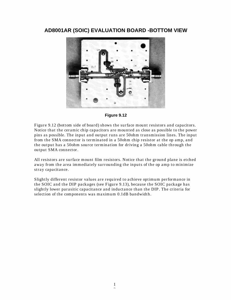
AD8001AR (SOIC) EVALUATION BOARD -BOTTOM VIEW
Figure 9.12
Figure 9.12 (bottom side of board) shows the surface mount resistors and capacitors.Notice that the ceramic chip capacitors are mounted as close as possible to the powerpins as possible. The input and output runs are 50ohm transmission lines. The inputfrom the SMA connector is terminated in a 50ohm chip resistor at the op amp, andthe output has a 50ohm source termination for driving a 50ohm cable through theoutput SMA connector.
All resistors are surface mount film resistors. Notice that the ground plane is etchedaway from the area immediately surrounding the inputs of the op amp to minimizestray capacitance.
Slightly different resistor values are required to achieve optimum performance inthe SOIC and the DIP packages (see Figure 9.13), because the SOIC package hasslightly lower parasitic capacitance and inductance than the DIP. The criteria forselection of the components was maximum 0.1dB bandwidth.
14
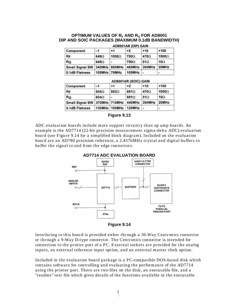
OPTIMUM VALUES OF RF AND RG FOR AD8001DIP AND SOIC PACKAGES (MAXIMUM 0.1dB BANDWIDTH)
Figure 9.13
ADC evaluation boards include more support circuitry than op amp boards. Anexample is the AD7714 (22-bit precision measurement sigma-delta ADC) evaluationboard (see Figure 9.14 for a simplified block diagram). Included on the evaluationboard are an AD780 precision reference, a 2.4576MHz crystal and digital buffers tobuffer the signal to and from the edge connectors.
AD7714 ADC EVALUATION BOARD
Figure 9.14
Interfacing to this board is provided either through a 36-Way Centronics connectoror through a 9-Way D-type connector. The Centronics connector is intended forconnection to the printer port of a PC. External sockets are provided for the analoginputs, an external reference input option, and an external master clock option.
Included in the evaluation board package is a PC-compatible DOS-based disk whichcontains software for controlling and evaluating the performance of the AD7714using the printer port. There are two files on the disk, an executable file, and a"readme" text file which gives details of the functions available in the executable
15
program. The evaluation software is run by running the executable file. Theprogram provides a number of different menu-type screens, each screen containingseveral function options.
The first menu gives options on the type of PC being used. The next menu in thesequence is the Main Menu which contains various options. These allow readingfrom the AD7714 Data Register, configuration of the Communications Register, fileoptions (read and write data to files), noise analysis, printer port setup, andresetting the AD7714.
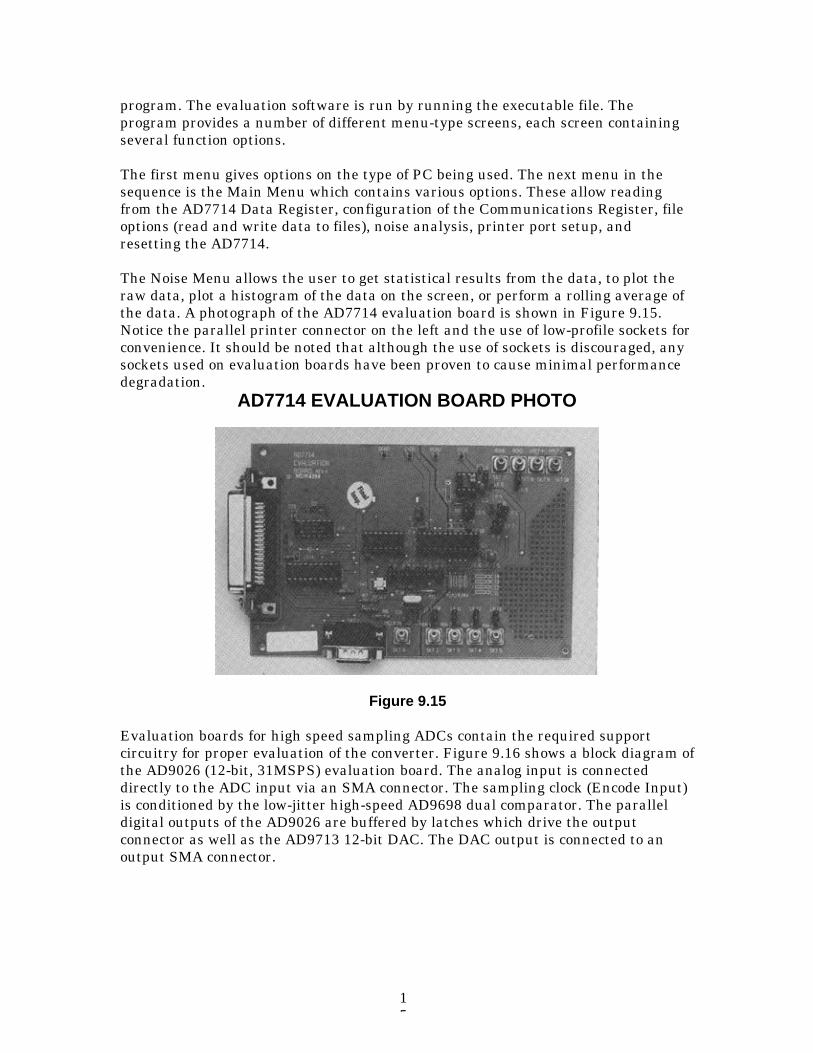
The Noise Menu allows the user to get statistical results from the data, to plot theraw data, plot a histogram of the data on the screen, or perform a rolling average ofthe data. A photograph of the AD7714 evaluation board is shown in Figure 9.15.Notice the parallel printer connector on the left and the use of low-profile sockets forconvenience. It should be noted that although the use of sockets is discouraged, anysockets used on evaluation boards have been proven to cause minimal performancedegradation.
AD7714 EVALUATION BOARD PHOTO
Figure 9.15
Evaluation boards for high speed sampling ADCs contain the required supportcircuitry for proper evaluation of the converter. Figure 9.16 shows a block diagram ofthe AD9026 (12-bit, 31MSPS) evaluation board. The analog input is connecteddirectly to the ADC input via an SMA connector. The sampling clock (Encode Input)is conditioned by the low-jitter high-speed AD9698 dual comparator. The paralleldigital outputs of the AD9026 are buffered by latches which drive the outputconnector as well as the AD9713 12-bit DAC. The DAC output is connected to anoutput SMA connector.
16
AD9026 12-BIT, 31MSPS ADC EVALUATION BOARD
Figure 9.16
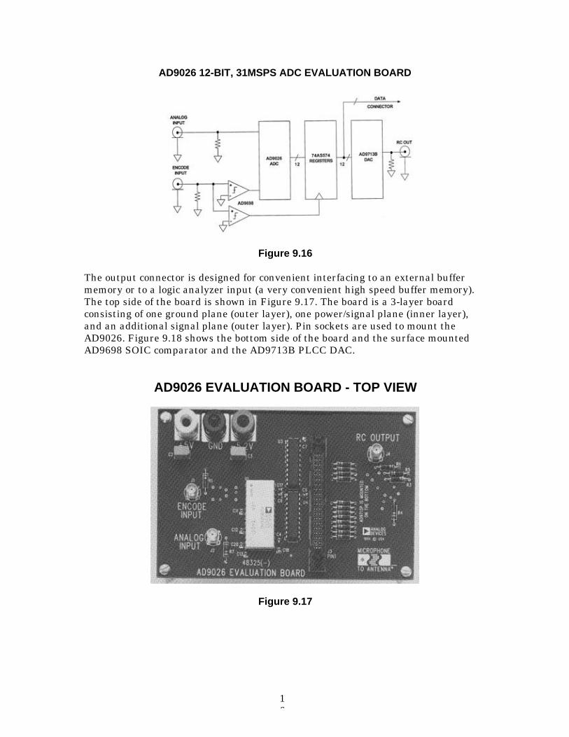
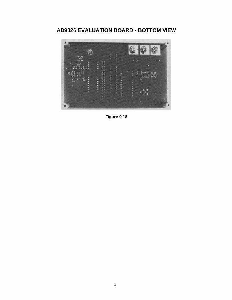
The output connector is designed for convenient interfacing to an external buffermemory or to a logic analyzer input (a very convenient high speed buffer memory).The top side of the board is shown in Figure 9.17. The board is a 3-layer boardconsisting of one ground plane (outer layer), one power/signal plane (inner layer),and an additional signal plane (outer layer). Pin sockets are used to mount theAD9026. Figure 9.18 shows the bottom side of the board and the surface mountedAD9698 SOIC comparator and the AD9713B PLCC DAC.
AD9026 EVALUATION BOARD - TOP VIEW
Figure 9.17
17
AD9026 EVALUATION BOARD - BOTTOM VIEW
Figure 9.18
18
REFERENCES: PROTOTYPING AND EVALUATIONBOARDS
1. Robert A. Pease, Troubleshooting Analog Circuits, Butterworth-Heinemann, 1991.
2. Wainwright Instruments Inc., 7770 Regents Rd., #113, Suite 371,San Diego, CA 92122, Tel. 619-558-1057, Fax. 619-558-1019.
Wainwright Instruments GmbH, Widdersberger Strasse 14,DW-8138 Andechs-Frieding, Germany. Tel: +49-8152-3162,Fax: +49-8152-40525.
3. Schematic Capture and Layout Software:
PADS Software, INC, 165 Forest St., Marlboro, MA, 01752
ACCEL Technologies, Inc., 6825 Flanders Dr., San Diego, CA,92121
4. Prototype Board Cutters:
LPKF CAD/CAM Systems, Inc., 1800 NW 169th Place,Beaverton, OR, 97006
T-Tech, Inc., 5591-B New Peachtree Road, Atlanta, GA,34341
19
NOISE REDUCTION AND FILTERING FOR SWITCHING
POWER SUPPLIES
Walt Jung and John McDonald
Precision analog circuitry has traditionally been powered from well regulated, lownoise linear power supplies. During the last decade however, switching powersupplies have become much more common in electronic systems. As a consequence,they also are being used for analog supplies. There are several good reasons for theirpopularity, including high efficiency, low temperature rise, small size, and lightweight.
Switching power supplies, or more simply switchers, a category including switchingregulators and switching converters, are by their nature efficient. Often this can beabove 90%, and as a result, these power supply types use less power and generateless heat than do equivalent linear supplies.
A switcher can be as much as one third the size and weight of a linear supplydelivering the same voltage and current. Switching frequencies can range from20kHz to 1MHz, and as a result, relatively small components can be used in theirdesign.
In spite of these benefits, switchers have their drawbacks, most notably high outputnoise. This noise generally extends over a broad band of frequencies, and occurs asboth conducted and radiated noise, and unwanted electric and magnetic fields.Voltage output noise of switching supplies are short-duration voltage transients, orspikes. Although the fundamental switching frequency can range from 20kHz to1MHz, the voltage spikes will contain frequency components extending easily to100MHz or more.
Because of wide variation in the noise output characteristics of commercialswitchers, they should always be purchased in accordance with a specification-control drawing. Although specifying switching supplies in terms of RMS noise iscommon vendor practice, as a user you should also specify the peak (or p-p)amplitudes of the switching spikes, with the output loading of your system. Youshould also insist that the switching-supply manufacturer inform you of any internalsupply design changes that may alter the spike amplitudes, duration, or switchingfrequency. These changes may require corresponding changes in external filteringnetworks.
20
SWITCHING POWER SUPPLY CHARACTERISTICS
ADVANTAGES:Efficient
Small Size, Light Weight
Low Operating Temperature Rise
Isolation from Line Transients
Wide Input/Output Range
DISADVANTAGES:Noise: LF, HF, Electric Field, Magnetic FieldConducted, Radiated
DC regulation and accuracy can be poor
Figure 9.19
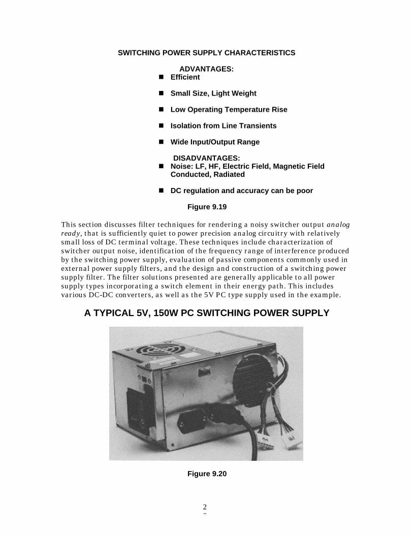
This section discusses filter techniques for rendering a noisy switcher output analogready, that is sufficiently quiet to power precision analog circuitry with relativelysmall loss of DC terminal voltage. These techniques include characterization ofswitcher output noise, identification of the frequency range of interference producedby the switching power supply, evaluation of passive components commonly used inexternal power supply filters, and the design and construction of a switching powersupply filter. The filter solutions presented are generally applicable to all powersupply types incorporating a switch element in their energy path. This includesvarious DC-DC converters, as well as the 5V PC type supply used in the example.
A TYPICAL 5V, 150W PC SWITCHING POWER SUPPLY
Figure 9.20
21
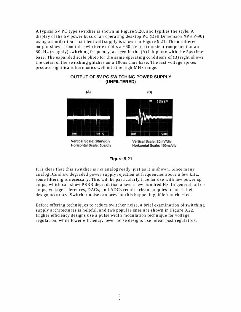
A typical 5V PC type switcher is shown in Figure 9.20, and typifies the style. Adisplay of the 5V power buss of an operating desktop PC (Dell Dimension XPS P-90)using a similar (but not identical) supply is shown in Figure 9.21. The unfilteredoutput shown from this switcher exhibits a ~60mV p-p transient component at an80kHz (roughly) switching frequency, as seen in the (A) left photo with the 5µs timebase. The expanded scale photo for the same operating conditions of (B) right showsthe detail of the switching glitches on a 100ns time base. The fast voltage spikesproduce significant harmonics well into the high MHz range.
OUTPUT OF 5V PC SWITCHING POWER SUPPLY(UNFILTERED)
Figure 9.21
It is clear that this switcher is not analog ready, just as it is shown. Since manyanalog ICs show degraded power supply rejection at frequencies above a few kHz,some filtering is necessary. This will be particularly true for use with low power opamps, which can show PSRR degradation above a few hundred Hz. In general, all opamps, voltage references, DACs, and ADCs require clean supplies to meet theirdesign accuracy. Switcher noise can prevent this happening, if left unchecked.
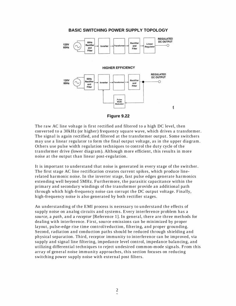
Before offering techniques to reduce switcher noise, a brief examination of switchingsupply architectures is helpful, and two popular ones are shown in Figure 9.22.Higher efficiency designs use a pulse width modulation technique for voltageregulation, while lower efficiency, lower noise designs use linear post regulators.
22
BASIC SWITCHING POWER SUPPLY TOPOLOGY
Figure 9.22
The raw AC line voltage is first rectified and filtered to a high DC level, thenconverted to a 30kHz (or higher) frequency square wave, which drives a transformer.The signal is again rectified, and filtered at the transformer output. Some switchersmay use a linear regulator to form the final output voltage, as in the upper diagram.Others use pulse width regulation techniques to control the duty cycle of thetransformer drive (lower diagram). Although more efficient, this results in morenoise at the output than linear post-regulation.
It is important to understand that noise is generated in every stage of the switcher.The first stage AC line rectification creates current spikes, which produce line-related harmonic noise. In the inverter stage, fast pulse edges generate harmonicsextending well beyond 5MHz. Furthermore, the parasitic capacitance within theprimary and secondary windings of the transformer provide an additional paththrough which high-frequency noise can corrupt the DC output voltage. Finally,high-frequency noise is also generated by both rectifier stages.
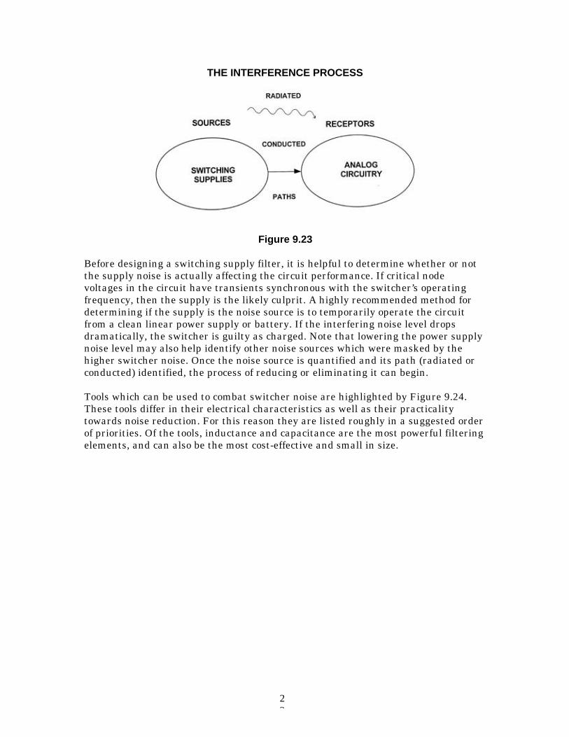
An understanding of the EMI process is necessary to understand the effects ofsupply noise on analog circuits and systems. Every interference problem has asource, a path, and a receptor [Reference 1]. In general, there are three methods fordealing with interference. First, source emissions can be minimized by properlayout, pulse-edge rise time control/reduction, filtering, and proper grounding.Second, radiation and conduction paths should be reduced through shielding andphysical separation. Third, receptor immunity to interference can be improved, viasupply and signal line filtering, impedance level control, impedance balancing, andutilizing differential techniques to reject undesired common-mode signals. From thisarray of general noise immunity approaches, this section focuses on reducingswitching power supply noise with external post filters.
23
THE INTERFERENCE PROCESS
Figure 9.23
Before designing a switching supply filter, it is helpful to determine whether or notthe supply noise is actually affecting the circuit performance. If critical nodevoltages in the circuit have transients synchronous with the switcher’s operatingfrequency, then the supply is the likely culprit. A highly recommended method fordetermining if the supply is the noise source is to temporarily operate the circuitfrom a clean linear power supply or battery. If the interfering noise level dropsdramatically, the switcher is guilty as charged. Note that lowering the power supplynoise level may also help identify other noise sources which were masked by thehigher switcher noise. Once the noise source is quantified and its path (radiated orconducted) identified, the process of reducing or eliminating it can begin.
Tools which can be used to combat switcher noise are highlighted by Figure 9.24.These tools differ in their electrical characteristics as well as their practicalitytowards noise reduction. For this reason they are listed roughly in a suggested orderof priorities. Of the tools, inductance and capacitance are the most powerful filteringelements, and can also be the most cost-effective and small in size.
24
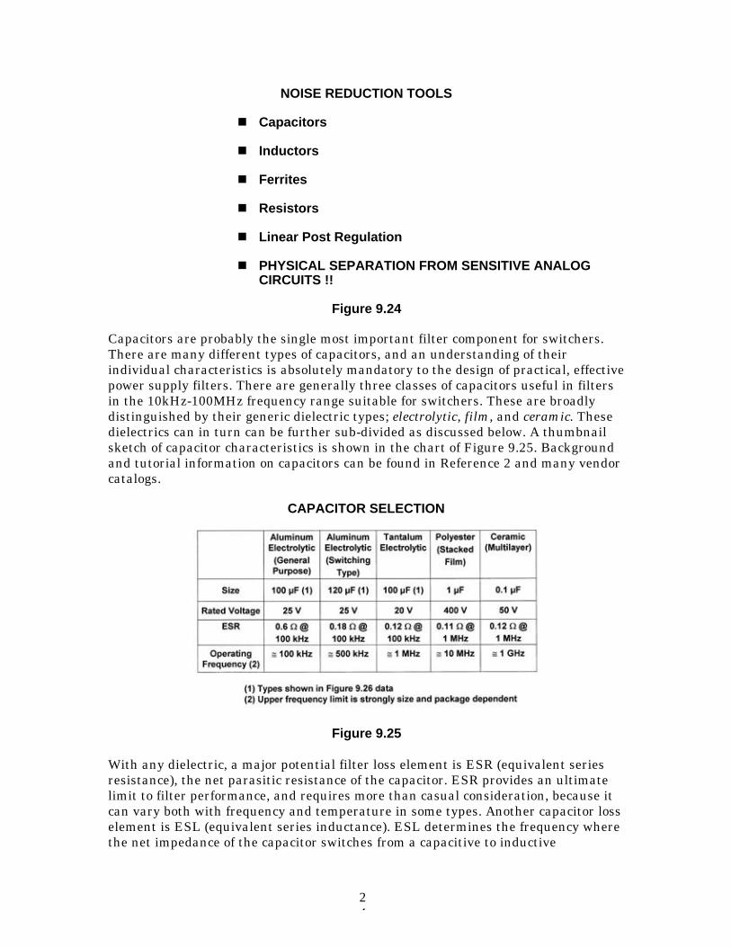
NOISE REDUCTION TOOLS
Capacitors
Inductors
Ferrites
Resistors
Linear Post Regulation
PHYSICAL SEPARATION FROM SENSITIVE ANALOGCIRCUITS !!
Figure 9.24
Capacitors are probably the single most important filter component for switchers.There are many different types of capacitors, and an understanding of theirindividual characteristics is absolutely mandatory to the design of practical, effectivepower supply filters. There are generally three classes of capacitors useful in filtersin the 10kHz-100MHz frequency range suitable for switchers. These are broadlydistinguished by their generic dielectric types; electrolytic, film, and ceramic. Thesedielectrics can in turn can be further sub-divided as discussed below. A thumbnailsketch of capacitor characteristics is shown in the chart of Figure 9.25. Backgroundand tutorial information on capacitors can be found in Reference 2 and many vendorcatalogs.
CAPACITOR SELECTION
Figure 9.25
With any dielectric, a major potential filter loss element is ESR (equivalent seriesresistance), the net parasitic resistance of the capacitor. ESR provides an ultimatelimit to filter performance, and requires more than casual consideration, because itcan vary both with frequency and temperature in some types. Another capacitor losselement is ESL (equivalent series inductance). ESL determines the frequency wherethe net impedance of the capacitor switches from a capacitive to inductive
25
characteristic. This varies from as low as 10kHz in some electrolytics to as high as100MHz or more in chip ceramic types. Both ESR and ESL are minimized when aleadless package is used, and all capacitor types discussed here are available insurface mount packages, which are preferable for high speed uses.
The electrolytic family provides an excellent, cost-effective low-frequency filtercomponent, because of the wide range of values, a high capacitance-to-volume ratio,and a broad range of working voltages. It includes general purpose aluminumelectrolytic types, available in working voltages from below 10V up to about 500V,and in size from 1 to several thousand µF (with proportional case sizes). Allelectrolytic capacitors are polarized, and thus cannot withstand more than a volt orso of reverse bias without damage. They have relatively high leakage currents (thiscan be tens of µA, but is strongly dependent upon specific family design, electricalsize and voltage rating vs. applied voltage). However, this is not likely to be a majorfactor for basic filtering applications.
Also included in the electrolytic family are tantalum types, which are generallylimited to voltages of 100V or less, with capacitance of 500µF or less[Reference 3]. Ina given size, tantalums exhibit a higher capacitance-to-volume ratios than do thegeneral purpose electrolytics, and have both a higher frequency range and lowerESR. They are generally more expensive than standard electrolytics, and must becarefully applied with respect to surge and ripple currents.
A subset of aluminum electrolytic capacitors is the switching type, which is designedand specified for handling high pulse currents at frequencies up to several hundredkHz with low losses [Reference 4]. This type of capacitor competes directly with thetantalum type in high frequency filtering applications, and has the advantage of amuch broader range of available values.
More recently, high performance aluminum electrolytic capacitors using an organicsemiconductor electrolyte have appeared [Reference 5]. These OS-CON families ofcapacitors feature appreciably lower ESR and higher frequency range than do theother electrolytic types, with an additional feature of low low-temperature ESRdegradation.
Film capacitors are available in very broad ranges of values and an array ofdielectrics, including polyester, polycarbonate, polypropylene, and polystyrene.Because of the low dielectric constant of these films, their volumetric efficiency isquite low, and a 10µF/50V polyester capacitor (for example) is actually a handful.Metalized (as opposed to foil) electrodes does help to reduce size, but even thehighest dielectric constant units among film types (polyester, polycarbonate) are stilllarger than any electrolytic, even using the thinnest films with the lowest voltageratings (50V). Where film types excel is in their low dielectric losses, a factor whichmay not necessarily be a practical advantage for filtering switchers. For example,ESR in film capacitors can be as low as 10milliohms or less, and the behavior offilms generally is very high in terms of Q. In fact, this can cause problems ofspurious resonance in filters, requiring damping components.
26
Typically using a wound layer-type construction, film capacitors can be inductive,which can limit their effectiveness for high frequency filtering. Obviously, only non-inductively made film caps are useful for switching regulator filters. One specificstyle which is non-inductive is the stacked-film type, where the capacitor plates arecut as small overlapping linear sheet sections from a much larger wound drum ofdielectric/plate material. This technique offers the low inductance attractiveness of aplate sheet style capacitor with conventional leads [see type “V” of Reference 4, plusReference 6]. Obviously, minimal lead length should be used for best high frequencyeffectiveness. Very high current polycarbonate film types are also available,specifically designed for switching power supplies, with a variety of low inductanceterminations to minimize ESL [Reference 7].
Dependent upon their electrical and physical size, film capacitors can be useful atfrequencies to well above 10MHz. At the very high frequencies, stacked film typesonly should be considered. Some manufacturers are also supplying film types inleadless surface mount packages, which eliminates the lead length inductance.
Ceramic is often the capacitor material of choice above a few MHz, due to itscompact size, low loss, and availability in values up to several µF in the high-Kdielectric formulations of X7R and Z5U, at voltage ratings up to 200V [see ceramicfamilies of Reference 3]. NP0 (also called COG) types use a lower dielectric constantformulation, and have nominally zero TC, plus a low voltage coefficient (unlike theless stable high-K types). The NP0 types are limited in available values to 0.1µF orless, with 0.01µF representing a more practical upper limit.
Multilayer ceramic “chip caps” are increasingly popular for bypassing and filteringat 10MHz or more, because their very low inductance design allows near optimumRF bypassing. In smaller values, ceramic chip caps have an operating frequencyrange to 1GHz. For these and other capacitors for high frequency applications, auseful value can be ensured by selecting a value which has a self-resonant frequencyabove the highest frequency of interest.
All capacitors have some finite ESR. In some cases, the ESR may actually be helpfulin reducing resonance peaks in filters, by supplying “free” damping. For example, ingeneral purpose, tantalum and switching type electrolytics, a broad series resonanceregion is noted in an impedance vs. frequency plot. This occurs where |Z| falls to aminimum level, which is nominally equal to the capacitor’s ESR at that frequency.In an example below, this low Q resonance is noted to encompass quite a widefrequency range, several octaves in fact. Contrasted to the very high Q sharpresonances of film and ceramic caps, this low Q behavior can be useful in controllingresonant peaks.
In most electrolytic capacitors, ESR degrades noticeably at low temperature, by asmuch as a factor of 4-6 times at –55°C vs. the room temperature value. For circuitswhere a high level of ESR is critical, this can lead to problems. Some specificelectrolytic types do address this problem, for example within the HFQ switchingtypes, the –10°C ESR at 100kHz is no more than 2× that at room temperature. TheOSCON electrolytics have a ESR vs. temperature characteristic which is relativelyflat.
27
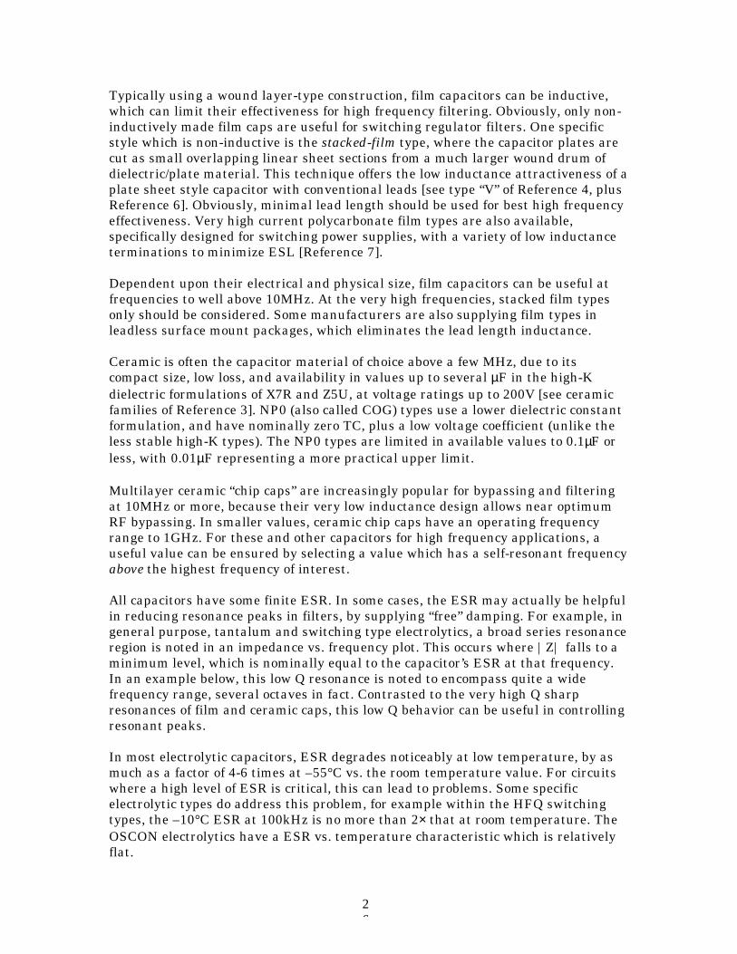
Figure 9.26 illustrates the high frequency impedance characteristics of a number ofelectrolytic capacitor types, using nominal 100µF/20V samples. In these plots, theimpedance, |Z|, vs. frequency over the 20Hz-200kHz range is displayed using ahigh resolution 4-terminal setup [Reference 8]. Shown in this display areperformance samples for a 100µF/25V general purpose aluminum unit (top curve @right), a 120µF/25V HFQ unit (next curve down @ right), a 100µF/20V tantalumbead type (next curve down @ right), and a 100µF/20V OS-CON unit (lowest curve @right). While the HFQ and tantalum samples are close in 100kHz impedance, thegeneral purpose unit is about 4 times worse. The OS-CON unit is nearly an order ofmagnitude lower in 100kHz impedance than the tantalum and switching electrolytictypes.
IMPEDANCE Z ( ) VS. FREQUENCY (Hz) FOR 100 FELECTROLYITC CAPACITORS (AC CURRENT = 50mA RMS)
Figure 9.26
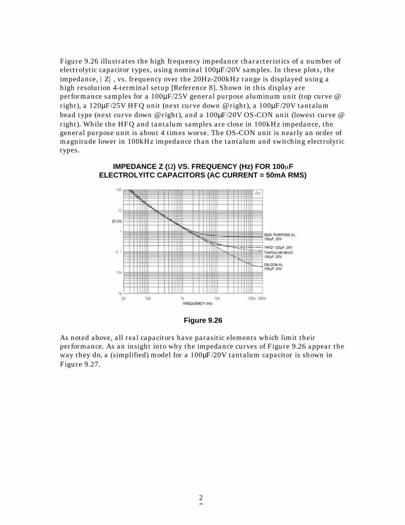
As noted above, all real capacitors have parasitic elements which limit theirperformance. As an insight into why the impedance curves of Figure 9.26 appear theway they do, a (simplified) model for a 100µF/20V tantalum capacitor is shown inFigure 9.27.
28
SIMPLIFIED SPICE MODEL FOR LEADED100 F/20V TANTALUM ELECTROLYTIC CAPACITOR
Figure 9.27
The electrical network representing this capacitor is shown, and it models the ESRand ESL components with simple R and L elements, plus a 1megohm shuntresistance. While this simple model ignores temperature and dielectric absorptioneffects which occur in the real capacitor, it is still sufficient for this discussion.
When driven with a constant level of AC current swept from 10Hz to 100MHz, thevoltage across this capacitor model is proportional to its net impedance, which isshown in Figure 9.28.
29
100 F / 20V TANTALUM CAPACITOR SIMPLIFIED MODELIMPEDANCE ( ) VS. FREQUENCY (Hz)
Figure 9.28
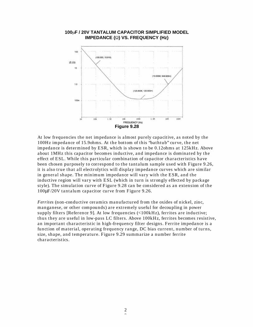
At low frequencies the net impedance is almost purely capacitive, as noted by the100Hz impedance of 15.9ohms. At the bottom of this “bathtub” curve, the netimpedance is determined by ESR, which is shown to be 0.12ohms at 125kHz. Aboveabout 1MHz this capacitor becomes inductive, and impedance is dominated by theeffect of ESL. While this particular combination of capacitor characteristics havebeen chosen purposely to correspond to the tantalum sample used with Figure 9.26,it is also true that all electrolytics will display impedance curves which are similarin general shape. The minimum impedance will vary with the ESR, and theinductive region will vary with ESL (which in turn is strongly effected by packagestyle). The simulation curve of Figure 9.28 can be considered as an extension of the100µF/20V tantalum capacitor curve from Figure 9.26.
Ferrites (non-conductive ceramics manufactured from the oxides of nickel, zinc,manganese, or other compounds) are extremely useful for decoupling in powersupply filters [Reference 9]. At low frequencies (<100kHz), ferrites are inductive;thus they are useful in low-pass LC filters. Above 100kHz, ferrites becomes resistive,an important characteristic in high-frequency filter designs. Ferrite impedance is afunction of material, operating frequency range, DC bias current, number of turns,size, shape, and temperature. Figure 9.29 summarize a number ferritecharacteristics.
30
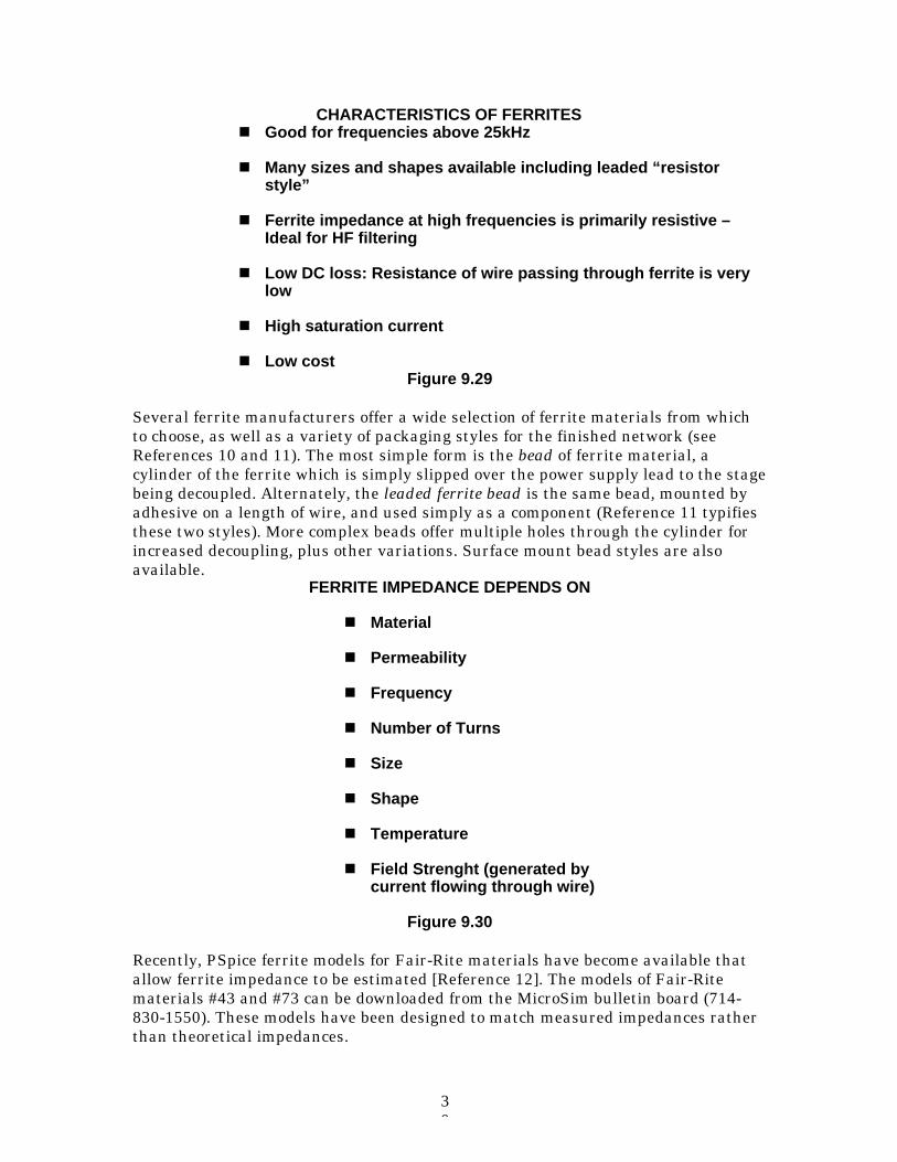
CHARACTERISTICS OF FERRITESGood for frequencies above 25kHz
Many sizes and shapes available including leaded “resistorstyle”
Ferrite impedance at high frequencies is primarily resistive –Ideal for HF filtering
Low DC loss: Resistance of wire passing through ferrite is verylow
High saturation current
Low costFigure 9.29
Several ferrite manufacturers offer a wide selection of ferrite materials from whichto choose, as well as a variety of packaging styles for the finished network (seeReferences 10 and 11). The most simple form is the bead of ferrite material, acylinder of the ferrite which is simply slipped over the power supply lead to the stagebeing decoupled. Alternately, the leaded ferrite bead is the same bead, mounted byadhesive on a length of wire, and used simply as a component (Reference 11 typifiesthese two styles). More complex beads offer multiple holes through the cylinder forincreased decoupling, plus other variations. Surface mount bead styles are alsoavailable.
FERRITE IMPEDANCE DEPENDS ON
Material
Permeability
Frequency
Number of Turns
Size
Shape
Temperature
Field Strenght (generated bycurrent flowing through wire)
Figure 9.30
Recently, PSpice ferrite models for Fair-Rite materials have become available thatallow ferrite impedance to be estimated [Reference 12]. The models of Fair-Ritematerials #43 and #73 can be downloaded from the MicroSim bulletin board (714-830-1550). These models have been designed to match measured impedances ratherthan theoretical impedances.
31
A ferrite’s impedance is dependent upon a number of inter-dependent variables, andis difficult to quantify analytically, thus selecting the proper ferrite is notstraightforward. However, knowing the following system characteristics will makeselection easier. First, determine the frequency range of the noise to be filtered. Aspectrum analyzer is useful here. Second, the expected temperature range of thefilter should be known, because ferrite impedance varies with temperature. Third,the DC bias current flowing through the ferrite must be known, to ensure that theferrite does not saturate. Although models and other analytical tools may proveuseful, the general guidelines given above, coupled with some experimentation withthe actual filter connected to the supply output under system load conditions, shouldultimately lead to the selection of the proper ferrite.
CHOOSING THE RIGHT FERRITE DEPENDS ON
Source of InterferenceInterference Frequency RangeImpedance Required at Interference FrequencyEnvironmental Conditions:
Temperature, AC and DC Field Strength, Size / Space Available
Don’t fail to Test the Design -------
EXPERIMENT! EXPERIMENT!
Figure 9.31
Maintaining high power supply efficiency requires the intelligent limiting of seriesresistors and linear post regulators in the switching supply’s output. However, smallresistors (generally less than 10ohms) can be used in applications where loadcurrents are low and load regulation is not highly critical.
Higher performance linear post regulators can provide 60dB and more of powersupply rejection up to 100kHz, for example see the designs of [Reference 8]. Whenused with effective input filtering, their PSRR can be extended above 1MHz orhigher. Linear post regulation will generally result in a net efficiency decrease,which can be serious if the regulator requires several volts of headroom. The PSRRvs. frequency performance of a linear post regulator should also be carefullyconsidered. For example, some low dropout linear regulators offer very little powersupply rejection at frequencies above a few kHz, a performance fact of life whichmust be traded off against the efficiency advantages of the <100mV level dropoutsthey can boast.
Using the component selection choices mentioned above, low and high frequencyband filters can be designed to smooth the noisy switcher’s DC output so as toproduce an analog ready 5V supply. It is most practical to do this over two (andsometimes more) stages, with each stage optimized for a range of frequencies. Onebasic stage can be used to carry all of the DC load current, and filter noise by 60dBor more up to about 10MHz. This larger filter is used as a card entry filter providingbroadband filtering for all analog power entering the PC board. Thereafter, smaller
32
and more simple local filter stages can be used to provide very high frequencydecoupling, right at the power pins of the individual ICs.
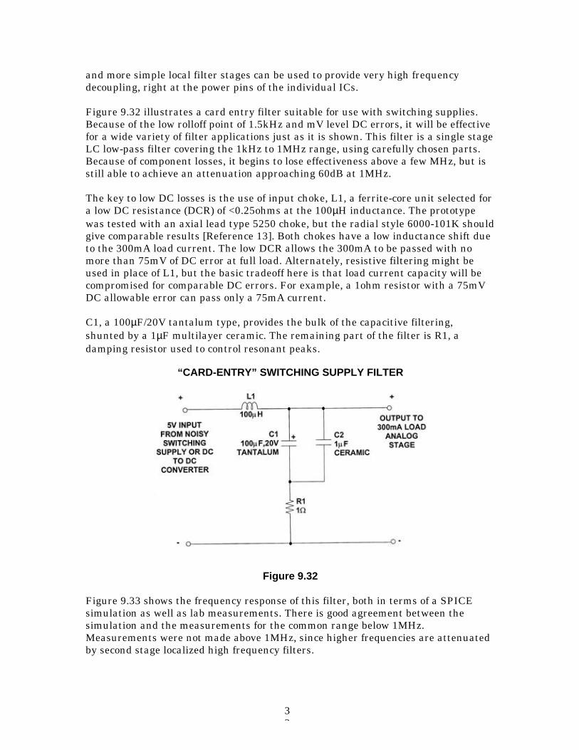
Figure 9.32 illustrates a card entry filter suitable for use with switching supplies.Because of the low rolloff point of 1.5kHz and mV level DC errors, it will be effectivefor a wide variety of filter applications just as it is shown. This filter is a single stageLC low-pass filter covering the 1kHz to 1MHz range, using carefully chosen parts.Because of component losses, it begins to lose effectiveness above a few MHz, but isstill able to achieve an attenuation approaching 60dB at 1MHz.
The key to low DC losses is the use of input choke, L1, a ferrite-core unit selected fora low DC resistance (DCR) of <0.25ohms at the 100µH inductance. The prototypewas tested with an axial lead type 5250 choke, but the radial style 6000-101K shouldgive comparable results [Reference 13]. Both chokes have a low inductance shift dueto the 300mA load current. The low DCR allows the 300mA to be passed with nomore than 75mV of DC error at full load. Alternately, resistive filtering might beused in place of L1, but the basic tradeoff here is that load current capacity will becompromised for comparable DC errors. For example, a 1ohm resistor with a 75mVDC allowable error can pass only a 75mA current.
C1, a 100µF/20V tantalum type, provides the bulk of the capacitive filtering,shunted by a 1µF multilayer ceramic. The remaining part of the filter is R1, adamping resistor used to control resonant peaks.
“CARD-ENTRY” SWITCHING SUPPLY FILTER
Figure 9.32
Figure 9.33 shows the frequency response of this filter, both in terms of a SPICEsimulation as well as lab measurements. There is good agreement between thesimulation and the measurements for the common range below 1MHz.Measurements were not made above 1MHz, since higher frequencies are attenuatedby second stage localized high frequency filters.
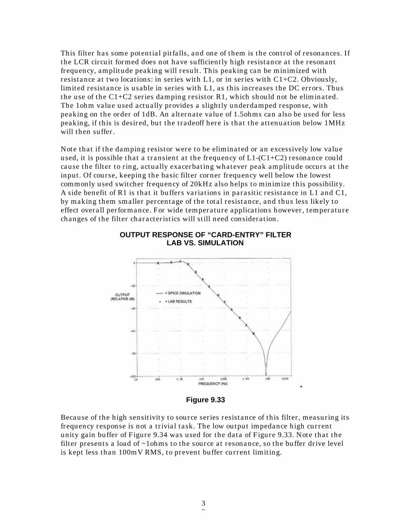
33
This filter has some potential pitfalls, and one of them is the control of resonances. Ifthe LCR circuit formed does not have sufficiently high resistance at the resonantfrequency, amplitude peaking will result. This peaking can be minimized withresistance at two locations: in series with L1, or in series with C1+C2. Obviously,limited resistance is usable in series with L1, as this increases the DC errors. Thusthe use of the C1+C2 series damping resistor R1, which should not be eliminated.The 1ohm value used actually provides a slightly underdamped response, withpeaking on the order of 1dB. An alternate value of 1.5ohms can also be used for lesspeaking, if this is desired, but the tradeoff here is that the attenuation below 1MHzwill then suffer.
Note that if the damping resistor were to be eliminated or an excessively low valueused, it is possible that a transient at the frequency of L1-(C1+C2) resonance couldcause the filter to ring, actually exacerbating whatever peak amplitude occurs at theinput. Of course, keeping the basic filter corner frequency well below the lowestcommonly used switcher frequency of 20kHz also helps to minimize this possibility.A side benefit of R1 is that it buffers variations in parasitic resistance in L1 and C1,by making them smaller percentage of the total resistance, and thus less likely toeffect overall performance. For wide temperature applications however, temperaturechanges of the filter characteristics will still need consideration.
OUTPUT RESPONSE OF “CARD-ENTRY” FILTERLAB VS. SIMULATION
Figure 9.33
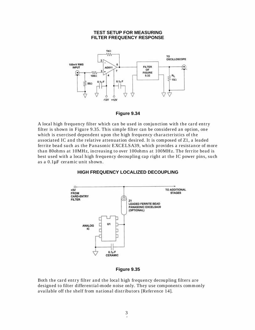
Because of the high sensitivity to source series resistance of this filter, measuring itsfrequency response is not a trivial task. The low output impedance high currentunity gain buffer of Figure 9.34 was used for the data of Figure 9.33. Note that thefilter presents a load of ~1ohms to the source at resonance, so the buffer drive levelis kept less than 100mV RMS, to prevent buffer current limiting.
34
TEST SETUP FOR MEASURINGFILTER FREQUENCY RESPONSE
Figure 9.34
A local high frequency filter which can be used in conjunction with the card entryfilter is shown in Figure 9.35. This simple filter can be considered an option, onewhich is exercised dependent upon the high frequency characteristics of theassociated IC and the relative attenuation desired. It is composed of Z1, a leadedferrite bead such as the Panasonic EXCELSA39, which provides a resistance of morethan 80ohms at 10MHz, increasing to over 100ohms at 100MHz. The ferrite bead isbest used with a local high frequency decoupling cap right at the IC power pins, suchas a 0.1µF ceramic unit shown.
HIGH FREQUENCY LOCALIZED DECOUPLING
Figure 9.35
Both the card entry filter and the local high frequency decoupling filters aredesigned to filter differential-mode noise only. They use components commonlyavailable off the shelf from national distributors [Reference 14].
35
The following is a list of switching power supply filter layout and constructionguidelines which will help guarantee that the filter does the best job possible:
(1) Pick the highest electrical value and voltage rating for filter capacitors which isconsistent with budget and space limits. This minimizes ESR, and maximizes filterperformance. Pick chokes for low inductance change at the rated DC current, as wellas low DCR.
(2) Use short and wide PCB tracks to decrease voltage drops and minimizeinductance. Make track widths at least 200 mils for every inch of track length forlowest DCR, and use 1 oz or 2 oz copper PCB traces to further reduce IR drops andinductance.
(3) Use short leads or leadless components, to minimize lead inductance. This willminimize the tendency to add excessive ESL and/or ESR. Surface mount packagesare preferred.
(4) Use a large-area ground plane for minimum impedance.
(5) Know what your components do over frequency, current and temperaturevariations! Make use of vendor component models for the simulation of prototypedesigns, and make sure that lab measurements correspond reasonably with thesimulation. While simulation is not absolutely necessary, it does instill confidence ina design when correlation is achieved (see Reference 15).
The discussion of switching power supplies so far has focused on filtering the outputof the supply. This assumes that the incoming AC power is relatively clean, anassumption not always valid. However, the AC power can also be an EMI path, bothentering and exiting the equipment. To remove this path and reduce emissionscaused by the switching power supply and other circuits in the instrument, a powerline filter is required. Remember that the AC line power can be lethal! Do notexperiment without proper equipment and training!
All components used in power line filters should be UL approved, and the best wayto provide this for your equipment is to specify only a complete, packaged ULapproved filter. It should be installed in such a manner that it is the first thing theAC line sees upon entering the equipment. Standard three wire IEC style line cordsare designed to mate with three terminal male connectors, which are integral tomany line filters. This is the best way to do this function, as this automaticallygrounds the third wire to the shell of the filter and equipment chassis via a lowinductance path.
36
POWER LINE FILTERING IS ALSO IMPORTANT
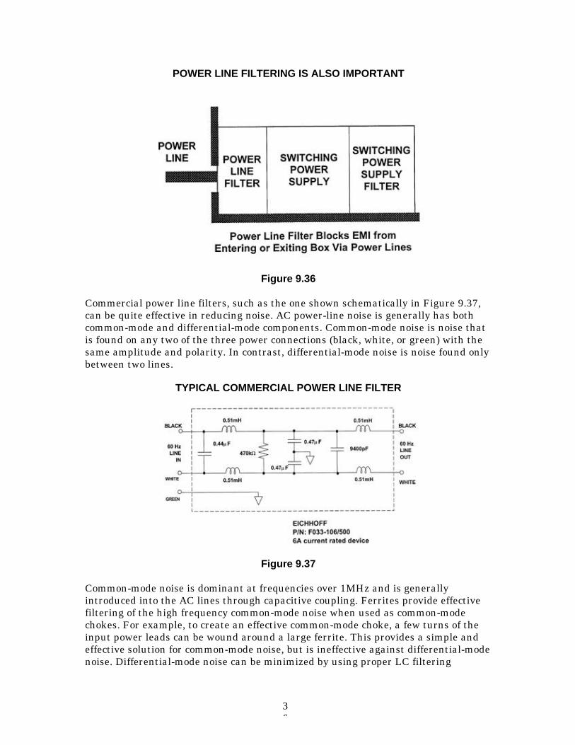
Figure 9.36
Commercial power line filters, such as the one shown schematically in Figure 9.37,can be quite effective in reducing noise. AC power-line noise is generally has bothcommon-mode and differential-mode components. Common-mode noise is noise thatis found on any two of the three power connections (black, white, or green) with thesame amplitude and polarity. In contrast, differential-mode noise is noise found onlybetween two lines.
TYPICAL COMMERCIAL POWER LINE FILTER
Figure 9.37
Common-mode noise is dominant at frequencies over 1MHz and is generallyintroduced into the AC lines through capacitive coupling. Ferrites provide effectivefiltering of the high frequency common-mode noise when used as common-modechokes. For example, to create an effective common-mode choke, a few turns of theinput power leads can be wound around a large ferrite. This provides a simple andeffective solution for common-mode noise, but is ineffective against differential-modenoise. Differential-mode noise can be minimized by using proper LC filtering
37
techniques as described earlier in this section, using proper UL approved across-the-line rated components. A power-line filter must be designed to minimize bothcommon- and differential-mode noise to keep EMI from entering and leaving thesystem.
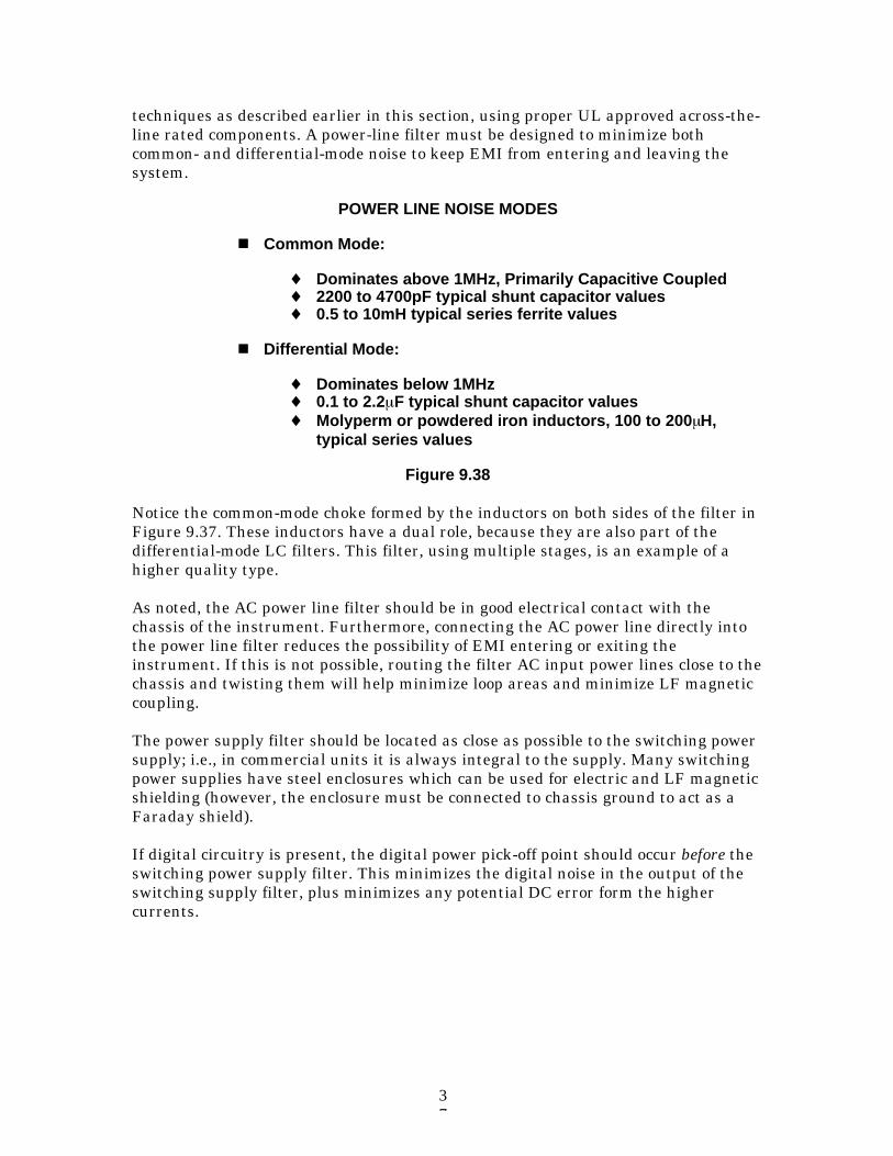
POWER LINE NOISE MODES
Common Mode:
Dominates above 1MHz, Primarily Capacitive Coupled2200 to 4700pF typical shunt capacitor values0.5 to 10mH typical series ferrite values
Differential Mode:
Dominates below 1MHz0.1 to 2.2 F typical shunt capacitor valuesMolyperm or powdered iron inductors, 100 to 200 H,typical series values
Figure 9.38
Notice the common-mode choke formed by the inductors on both sides of the filter inFigure 9.37. These inductors have a dual role, because they are also part of thedifferential-mode LC filters. This filter, using multiple stages, is an example of ahigher quality type.
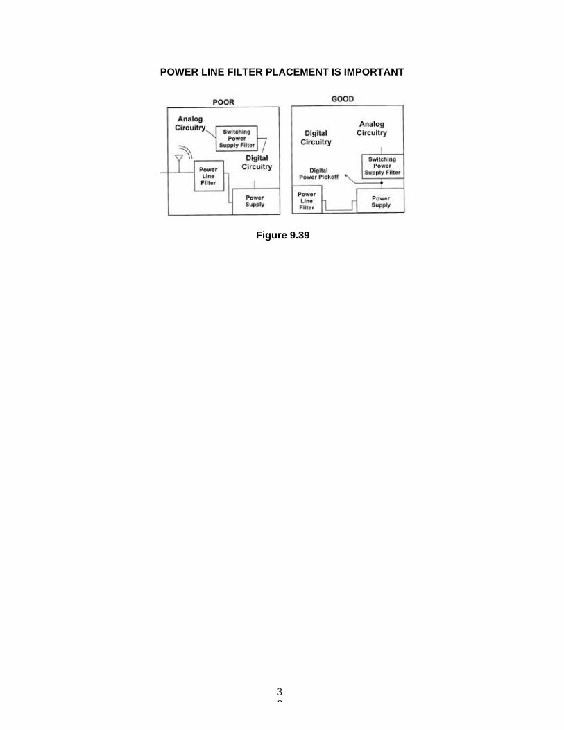
As noted, the AC power line filter should be in good electrical contact with thechassis of the instrument. Furthermore, connecting the AC power line directly intothe power line filter reduces the possibility of EMI entering or exiting theinstrument. If this is not possible, routing the filter AC input power lines close to thechassis and twisting them will help minimize loop areas and minimize LF magneticcoupling.
The power supply filter should be located as close as possible to the switching powersupply; i.e., in commercial units it is always integral to the supply. Many switchingpower supplies have steel enclosures which can be used for electric and LF magneticshielding (however, the enclosure must be connected to chassis ground to act as aFaraday shield).
If digital circuitry is present, the digital power pick-off point should occur before theswitching power supply filter. This minimizes the digital noise in the output of theswitching supply filter, plus minimizes any potential DC error form the highercurrents.
38
POWER LINE FILTER PLACEMENT IS IMPORTANT
Figure 9.39
39
REFERENCES: NOISE REDUCTION AND FILTERING FORSWITCHING POWER SUPPLIES
1. EMC Design Workshop Notes, Kimmel-Gerke Associates, Ltd.,St. Paul, MN. 55108, (612) 330-3728.
2. Walt Jung, Dick Marsh, Picking Capacitors, Parts 1 & 2, Audio,February, March, 1980.
3. Tantalum Electrolytic and Ceramic Capacitor Families, KemetElectronics, Box 5928, Greenville, SC, 29606, (803) 963-6300.
4. Type HFQ Aluminum Electrolytic Capacitor and type V StackedPolyester Film Capacitor, Panasonic, 2 Panasonic Way, Secaucus,NJ, 07094, (201) 348-7000.
5. OS-CON Aluminum Electrolytic Capacitor 93/94 Technical Book,Sanyo, 3333 Sanyo Road, Forrest City, AK, 72335, (501) 633-6634.
6. Ian Clelland, Metalized Polyester Film Capacitor Fills High FrequencySwitcher Needs, PCIM, June 1992.
7. Type 5MC Metallized Polycarbonate Capacitor, Electronic Concepts, Inc.,Box 1278, Eatontown, NJ, 07724, (908) 542-7880.
8. Walt Jung, Regulators for High-Performance Audio, Parts 1 and 2,The Audio Amateur, issues 1 and 2, 1995.
9. Henry Ott, Noise Reduction Techniques in Electronic Systems,2d Ed., 1988, Wiley.
10. Fair-Rite Linear Ferrites Catalog, Fair-Rite Products, Box J, Wallkill,NY, 12886, (914) 895-2055.
11. Type EXCEL leaded ferrite bead EMI filter, and type EXC L leadlessferrite bead, Panasonic, 2 Panasonic Way, Secaucus, NJ, 07094,(201) 348-7000.
12. Steve Hageman, Use Ferrite Bead Models to Analyze EMI Suppression,The Design Center Source, MicroSim Newsletter, January, 1995.
13. Type 5250 and 6000-101K chokes, J. W. Miller, 306 E. Alondra Blvd.,Gardena, CA, 90247, (310) 515-1720.
14. DIGI-KEY, PO Box 677, Thief River Falls, MN, 56701-0677,(800) 344-4539.
15. Tantalum Electrolytic Capacitor SPICE Models, Kemet Electronics,Box 5928, Greenville, SC, 29606, (803) 963-6300.
40
16. Eichhoff Electronics, Inc., 205 Hallene Road, Warwick, RI., 02886,(401) 738-1440.
41
LOW DROPOUT REFERENCES ANDREGULATORSWalt Jung
Many circuits require stable regulated voltages relatively close in potential to anunregulated source. An example would be a linear post regulator for a switchingpower supply, where voltage loss is critical. This low dropout type of regulator isreadily implemented with a rail-rail output op amp. The wide output swing and lowsaturation voltage enables outputs to come within a fraction of a volt of the sourcefor medium current (<30mA) loads, such as reference applications. For higher outputcurrents, the rail-rail voltage swing feature allows direct drive to low saturationvoltage pass devices, such as power PNPs or P-channel MOSFETs. Op amps whichwork from 3V up with the rail-rail features are most suitable here, providing powereconomy and maximum flexibility.
BASIC REFERENCES IN LOW POWER SYSTEMS
Among the many problems in making stable DC voltage references work from 5Vand lower supplies are quiescent power consumption, overall efficiency, the ability tooperate down to 3V, low input/output (dropout) capability, and minimum noiseoutput. Because such low voltage supplies can't support 6V zeners, these low voltagereferences must necessarily be bandgap based-- a 1.2V potential.
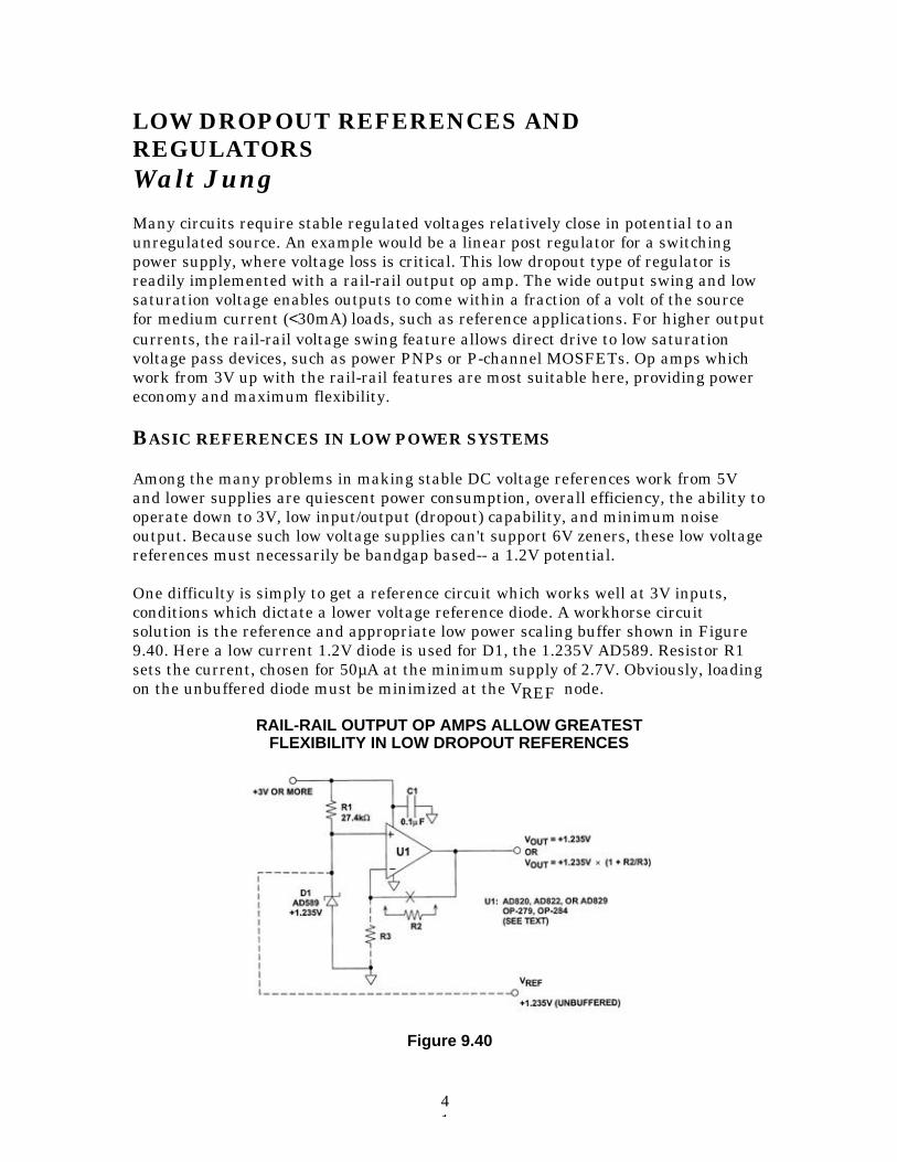
One difficulty is simply to get a reference circuit which works well at 3V inputs,conditions which dictate a lower voltage reference diode. A workhorse circuitsolution is the reference and appropriate low power scaling buffer shown in Figure9.40. Here a low current 1.2V diode is used for D1, the 1.235V AD589. Resistor R1sets the current, chosen for 50µA at the minimum supply of 2.7V. Obviously, loadingon the unbuffered diode must be minimized at the VREF node.
RAIL-RAIL OUTPUT OP AMPS ALLOW GREATESTFLEXIBILITY IN LOW DROPOUT REFERENCES
Figure 9.40
42
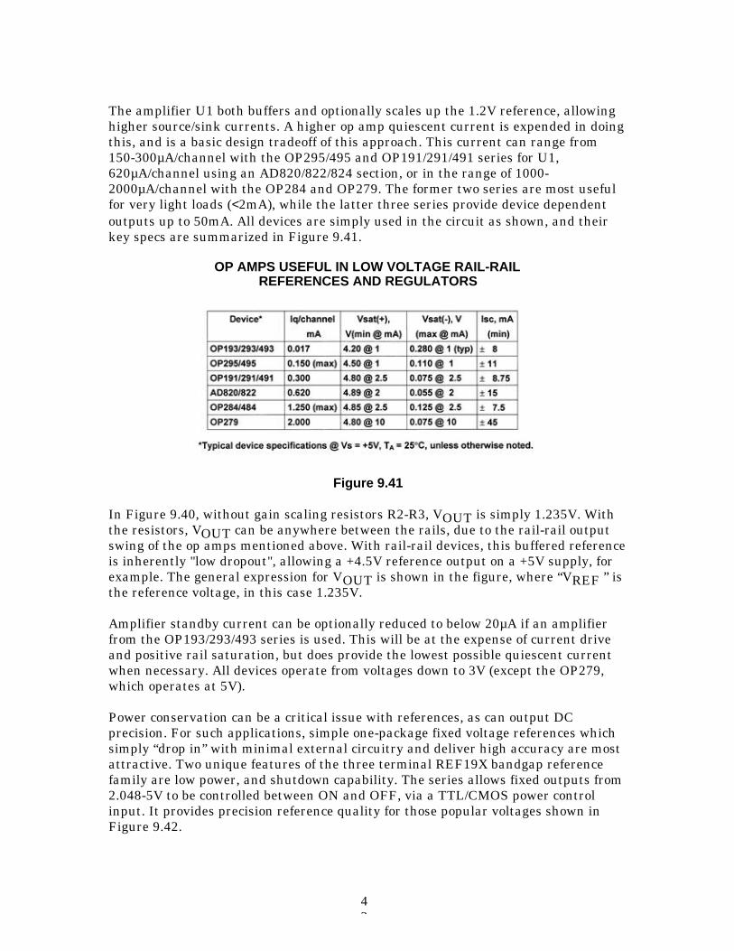
The amplifier U1 both buffers and optionally scales up the 1.2V reference, allowinghigher source/sink currents. A higher op amp quiescent current is expended in doingthis, and is a basic design tradeoff of this approach. This current can range from150-300µA/channel with the OP295/495 and OP191/291/491 series for U1,620µA/channel using an AD820/822/824 section, or in the range of 1000-2000µA/channel with the OP284 and OP279. The former two series are most usefulfor very light loads (<2mA), while the latter three series provide device dependentoutputs up to 50mA. All devices are simply used in the circuit as shown, and theirkey specs are summarized in Figure 9.41.
OP AMPS USEFUL IN LOW VOLTAGE RAIL-RAILREFERENCES AND REGULATORS
Figure 9.41
In Figure 9.40, without gain scaling resistors R2-R3, VOUT is simply 1.235V. Withthe resistors, VOUT can be anywhere between the rails, due to the rail-rail outputswing of the op amps mentioned above. With rail-rail devices, this buffered referenceis inherently "low dropout", allowing a +4.5V reference output on a +5V supply, forexample. The general expression for VOUT is shown in the figure, where “VREF ” isthe reference voltage, in this case 1.235V.
Amplifier standby current can be optionally reduced to below 20µA if an amplifierfrom the OP193/293/493 series is used. This will be at the expense of current driveand positive rail saturation, but does provide the lowest possible quiescent currentwhen necessary. All devices operate from voltages down to 3V (except the OP279,which operates at 5V).
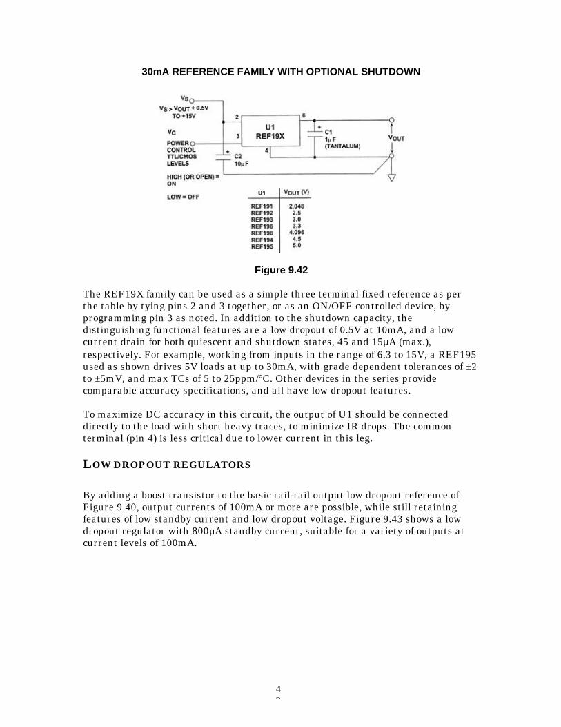
Power conservation can be a critical issue with references, as can output DCprecision. For such applications, simple one-package fixed voltage references whichsimply “drop in” with minimal external circuitry and deliver high accuracy are mostattractive. Two unique features of the three terminal REF19X bandgap referencefamily are low power, and shutdown capability. The series allows fixed outputs from2.048-5V to be controlled between ON and OFF, via a TTL/CMOS power controlinput. It provides precision reference quality for those popular voltages shown inFigure 9.42.
43
30mA REFERENCE FAMILY WITH OPTIONAL SHUTDOWN
Figure 9.42
The REF19X family can be used as a simple three terminal fixed reference as perthe table by tying pins 2 and 3 together, or as an ON/OFF controlled device, byprogramming pin 3 as noted. In addition to the shutdown capacity, thedistinguishing functional features are a low dropout of 0.5V at 10mA, and a lowcurrent drain for both quiescent and shutdown states, 45 and 15µA (max.),respectively. For example, working from inputs in the range of 6.3 to 15V, a REF195used as shown drives 5V loads at up to 30mA, with grade dependent tolerances of ±2to ±5mV, and max TCs of 5 to 25ppm/°C. Other devices in the series providecomparable accuracy specifications, and all have low dropout features.
To maximize DC accuracy in this circuit, the output of U1 should be connecteddirectly to the load with short heavy traces, to minimize IR drops. The commonterminal (pin 4) is less critical due to lower current in this leg.
LOW DROPOUT REGULATORS
By adding a boost transistor to the basic rail-rail output low dropout reference ofFigure 9.40, output currents of 100mA or more are possible, while still retainingfeatures of low standby current and low dropout voltage. Figure 9.43 shows a lowdropout regulator with 800µA standby current, suitable for a variety of outputs atcurrent levels of 100mA.
44
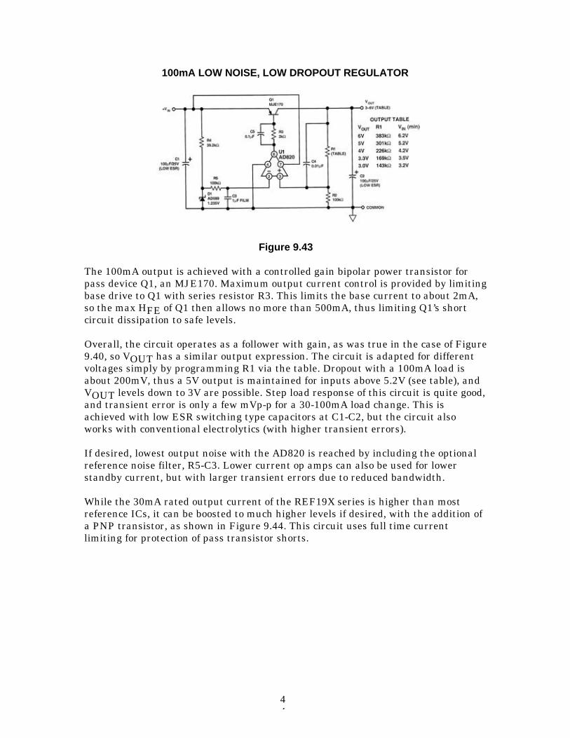
100mA LOW NOISE, LOW DROPOUT REGULATOR
Figure 9.43
The 100mA output is achieved with a controlled gain bipolar power transistor forpass device Q1, an MJE170. Maximum output current control is provided by limitingbase drive to Q1 with series resistor R3. This limits the base current to about 2mA,so the max HFE of Q1 then allows no more than 500mA, thus limiting Q1’s shortcircuit dissipation to safe levels.
Overall, the circuit operates as a follower with gain, as was true in the case of Figure9.40, so VOUT has a similar output expression. The circuit is adapted for differentvoltages simply by programming R1 via the table. Dropout with a 100mA load isabout 200mV, thus a 5V output is maintained for inputs above 5.2V (see table), andVOUT levels down to 3V are possible. Step load response of this circuit is quite good,and transient error is only a few mVp-p for a 30-100mA load change. This isachieved with low ESR switching type capacitors at C1-C2, but the circuit alsoworks with conventional electrolytics (with higher transient errors).
If desired, lowest output noise with the AD820 is reached by including the optionalreference noise filter, R5-C3. Lower current op amps can also be used for lowerstandby current, but with larger transient errors due to reduced bandwidth.
While the 30mA rated output current of the REF19X series is higher than mostreference ICs, it can be boosted to much higher levels if desired, with the addition ofa PNP transistor, as shown in Figure 9.44. This circuit uses full time currentlimiting for protection of pass transistor shorts.
45
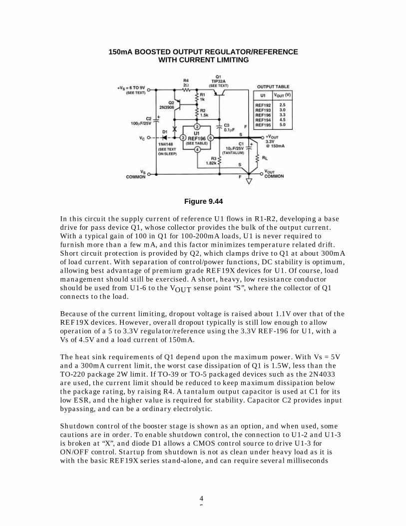
150mA BOOSTED OUTPUT REGULATOR/REFERENCEWITH CURRENT LIMITING
Figure 9.44
In this circuit the supply current of reference U1 flows in R1-R2, developing a basedrive for pass device Q1, whose collector provides the bulk of the output current.With a typical gain of 100 in Q1 for 100-200mA loads, U1 is never required tofurnish more than a few mA, and this factor minimizes temperature related drift.Short circuit protection is provided by Q2, which clamps drive to Q1 at about 300mAof load current. With separation of control/power functions, DC stability is optimum,allowing best advantage of premium grade REF19X devices for U1. Of course, loadmanagement should still be exercised. A short, heavy, low resistance conductorshould be used from U1-6 to the VOUT sense point “S”, where the collector of Q1connects to the load.
Because of the current limiting, dropout voltage is raised about 1.1V over that of theREF19X devices. However, overall dropout typically is still low enough to allowoperation of a 5 to 3.3V regulator/reference using the 3.3V REF-196 for U1, with aVs of 4.5V and a load current of 150mA.
The heat sink requirements of Q1 depend upon the maximum power. With Vs = 5Vand a 300mA current limit, the worst case dissipation of Q1 is 1.5W, less than theTO-220 package 2W limit. If TO-39 or TO-5 packaged devices such as the 2N4033are used, the current limit should be reduced to keep maximum dissipation belowthe package rating, by raising R4. A tantalum output capacitor is used at C1 for itslow ESR, and the higher value is required for stability. Capacitor C2 provides inputbypassing, and can be a ordinary electrolytic.
Shutdown control of the booster stage is shown as an option, and when used, somecautions are in order. To enable shutdown control, the connection to U1-2 and U1-3is broken at “X”, and diode D1 allows a CMOS control source to drive U1-3 forON/OFF control. Startup from shutdown is not as clean under heavy load as it iswith the basic REF19X series stand-alone, and can require several milliseconds
46
under load. Nevertheless, it is still effective, and can fully control 150mA loads.When shutdown control is used, heavy capacitive loads should be minimized.
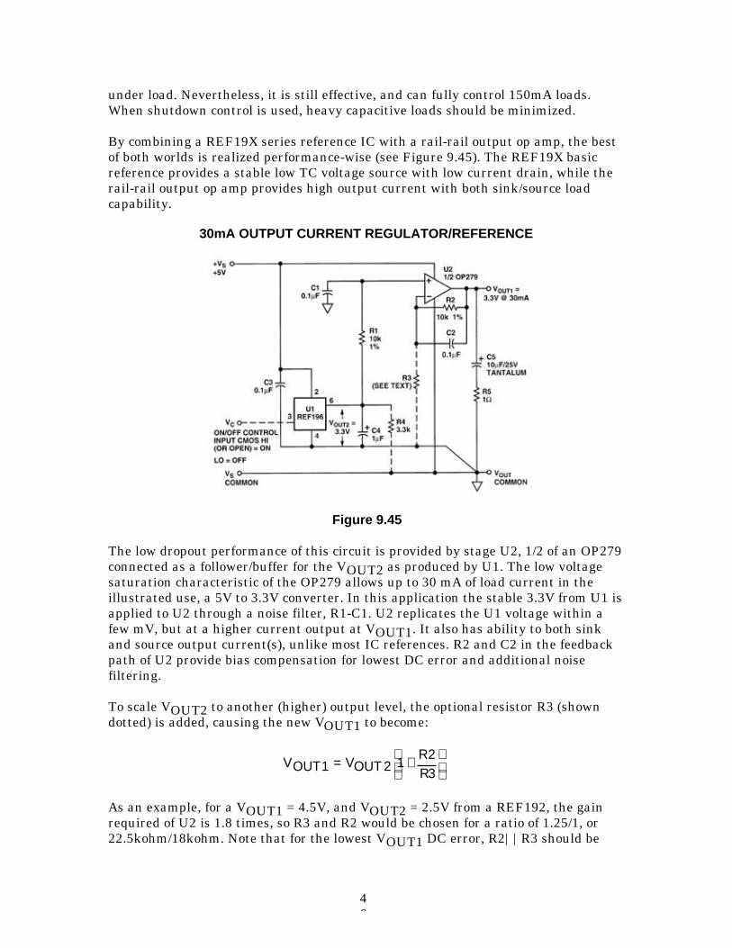
By combining a REF19X series reference IC with a rail-rail output op amp, the bestof both worlds is realized performance-wise (see Figure 9.45). The REF19X basicreference provides a stable low TC voltage source with low current drain, while therail-rail output op amp provides high output current with both sink/source loadcapability.
30mA OUTPUT CURRENT REGULATOR/REFERENCE
Figure 9.45
The low dropout performance of this circuit is provided by stage U2, 1/2 of an OP279connected as a follower/buffer for the VOUT2 as produced by U1. The low voltagesaturation characteristic of the OP279 allows up to 30 mA of load current in theillustrated use, a 5V to 3.3V converter. In this application the stable 3.3V from U1 isapplied to U2 through a noise filter, R1-C1. U2 replicates the U1 voltage within afew mV, but at a higher current output at VOUT1. It also has ability to both sinkand source output current(s), unlike most IC references. R2 and C2 in the feedbackpath of U2 provide bias compensation for lowest DC error and additional noisefiltering.
To scale VOUT2 to another (higher) output level, the optional resistor R3 (showndotted) is added, causing the new VOUT1 to become:
VOUT VOUTRR1 2 1
23
= +
As an example, for a VOUT1 = 4.5V, and VOUT2 = 2.5V from a REF192, the gainrequired of U2 is 1.8 times, so R3 and R2 would be chosen for a ratio of 1.25/1, or22.5kohm/18kohm. Note that for the lowest VOUT1 DC error, R2||R3 should be
47
maintained equal to R1 (as here), and the R2-R3 resistors should be stable, closetolerance metal film types.
Performance of the circuit is good in both AC and DC senses, with the measured DCoutput change for a 30mA load change under 1mV, equivalent to an outputimpedance of <0.03ohm. The transient performance for a step change of 0-10mA ofload current is determined largely by the R5-C5 output network. With the valuesshown, the transient is about 10mV peak, and settles to within 2mV in 8µs, foreither polarity. Further reduction in transient amplitude is possible by reducing R5and possibly increasing C3, but this should be verified by experiment to minimizeexcessive ringing with some capacitor types. Load current step changes smaller than10mA will of course show less transient error.
The circuit can be used either as shown as a 5 to 3.3V reference/regulator, or it canalso be used with ON/OFF control. By driving pin 3 of U1 with a logic control signalas noted, the output is switched ON/OFF. Note that when ON/OFF control is used,resistor R4 must be used with U1, to speed ON-OFF switching.
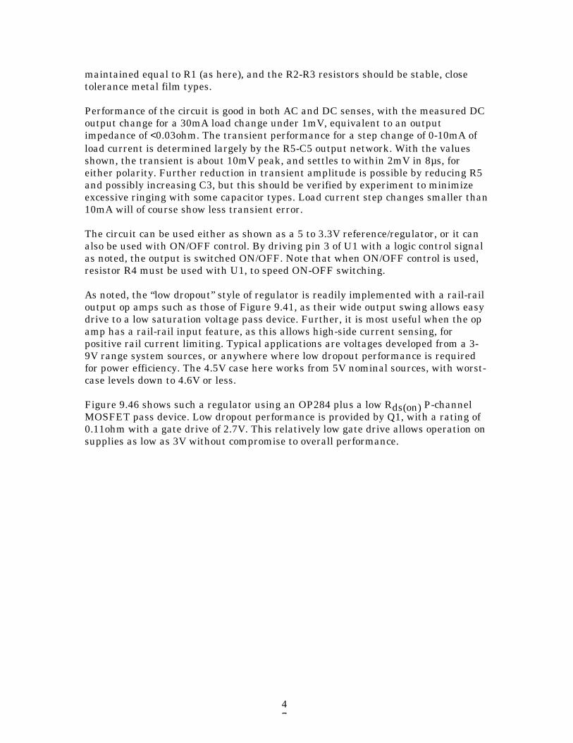
As noted, the “low dropout” style of regulator is readily implemented with a rail-railoutput op amps such as those of Figure 9.41, as their wide output swing allows easydrive to a low saturation voltage pass device. Further, it is most useful when the opamp has a rail-rail input feature, as this allows high-side current sensing, forpositive rail current limiting. Typical applications are voltages developed from a 3-9V range system sources, or anywhere where low dropout performance is requiredfor power efficiency. The 4.5V case here works from 5V nominal sources, with worst-case levels down to 4.6V or less.
Figure 9.46 shows such a regulator using an OP284 plus a low Rds(on) P-channelMOSFET pass device. Low dropout performance is provided by Q1, with a rating of0.11ohm with a gate drive of 2.7V. This relatively low gate drive allows operation onsupplies as low as 3V without compromise to overall performance.
48
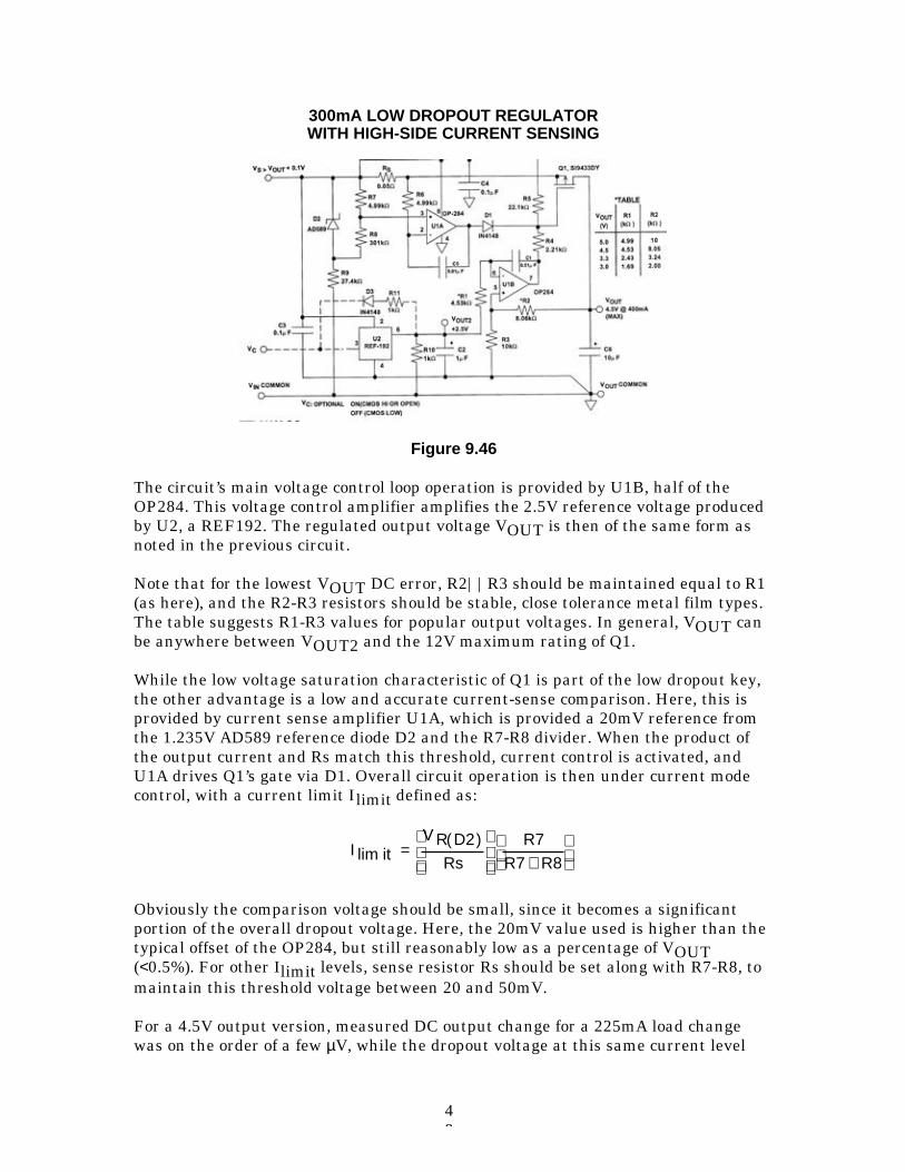
300mA LOW DROPOUT REGULATORWITH HIGH-SIDE CURRENT SENSING
Figure 9.46
The circuit’s main voltage control loop operation is provided by U1B, half of theOP284. This voltage control amplifier amplifies the 2.5V reference voltage producedby U2, a REF192. The regulated output voltage VOUT is then of the same form asnoted in the previous circuit.
Note that for the lowest VOUT DC error, R2||R3 should be maintained equal to R1(as here), and the R2-R3 resistors should be stable, close tolerance metal film types.The table suggests R1-R3 values for popular output voltages. In general, VOUT canbe anywhere between VOUT2 and the 12V maximum rating of Q1.
While the low voltage saturation characteristic of Q1 is part of the low dropout key,the other advantage is a low and accurate current-sense comparison. Here, this isprovided by current sense amplifier U1A, which is provided a 20mV reference fromthe 1.235V AD589 reference diode D2 and the R7-R8 divider. When the product ofthe output current and Rs match this threshold, current control is activated, andU1A drives Q1’s gate via D1. Overall circuit operation is then under current modecontrol, with a current limit Ilimit defined as:
I itV R D
Rs
R
R Rlim( )=
+
2 7
7 8
Obviously the comparison voltage should be small, since it becomes a significantportion of the overall dropout voltage. Here, the 20mV value used is higher than thetypical offset of the OP284, but still reasonably low as a percentage of VOUT(<0.5%). For other Ilimit levels, sense resistor Rs should be set along with R7-R8, tomaintain this threshold voltage between 20 and 50mV.
For a 4.5V output version, measured DC output change for a 225mA load changewas on the order of a few µV, while the dropout voltage at this same current level
49
was about 30mV. The current limit as shown is 400mA, allowing operation at levelsup to 300mA or more. While the Q1 device can support currents of several amperes,a practical current rating takes into account the SO-8 device’s 2.5W 25°Cdissipation. A short-circuit current of 400mA at an input level of 5V will cause a 2Wdissipation in Q1, so other input conditions should be considered carefully in termsof Q1’s potential overheating. If higher powered devices are used for Q1, the circuitwill support outputs of tens of amperes as well as the higher VOUT levels notedabove.
The circuit can be used either as shown for a standard low dropout regulator, or itcan also be used with ON/OFF control. Note that when the output is OFF in thiscircuit, it is still active (i.e., not an open circuit). This is because the OFF statesimply reduces the voltage input to R1, leaving the U1A/B amplifiers and Q1 stillactive.
When ON/OFF control is used, resistor R10 should be used with U1, to speed ON-OFF switching, and to allow the output of the circuit to settle to a nominal zerovoltage. Components D3 and R11 also aid in speeding up the ON-OFF transition, byproviding a dynamic discharge path for C2. OFF-ON transition time is less than1ms, while the ON-OFF transition is longer, but under 10ms.
50
REFERENCES: LOW DROPOUT REFERENCES ANDREGULATORS 1. Walt Jung, Build an Ultra-Low-Noise Voltage Reference,
Electronic Design Analog Applications Issue, June 24, 1993.
2. Walt Jung, Getting the Most from IC Voltage References, AnalogDialogue 28-1, 1994.
3. Walt Jung, The Ins and Outs of ‘Green’ Regulators/References ,Electronic Design Analog Applications Issue, June 27, 1994.
4. Walt Jung, Very-Low-Noise 5-V Regulator, Electronic Design,July 25, 1994.
51
EMI/RFI CONSIDERATIONSAdolfo A. Garcia
Electromagnetic interference (EMI) has become a hot topic in the last few yearsamong circuit designers and systems engineers. Although the subject matter andprior art have been in existence for over the last 50 years or so, the advent ofportable and high-frequency industrial and consumer electronics has provided acomfortable standard of living for many EMI testing engineers, consultants, andpublishers. With the help of EDN Magazine and Kimmel Gerke Associates, thissection will highlight general issues of EMC (electrom agnetic compatibility) tofamiliarize the system/circuit designer with this subject and to illustrate proventechniques for protection against EMI.
A PRIMER ON EMI REGULATIONS
The intent of this section is to summarize the different types of electromagneticcompatibility (EMC) regulations imposed on equipment manufacturers, bothvoluntary and mandatory. Published EMC regulations apply at this time only toequipment and systems, and not to components. Thus, EMI hardened equipmentdoes not necessarily imply that each of the components used (integrated circuits,especially) in the equipment must also be EMI hardened.
Commercial Equipment
The two driving forces behind commercial EMI regulations are the FCC (FederalCommunications Commission) in the U. S. and the VDE (Verband DeutscherElectrotechniker) in Germany. VDE regulations are more restrictive than the FCC’swith regard to emissions and radiation, but the European Community will beadding immunity to RF, electrostatic discharge, and power-line disturbances to theVDE regulations, and will require mandatory compliance in 1996. In Japan,commercial EMC regulations are covered under the VCCI (Voluntary ControlCouncil for Interference) standards and, implied by the name, are much looser thantheir FCC and VDE counterparts.
All commercial EMI regulations primarily focus on radiated emissions, specificallyto protect nearby radio and television receivers, although both FCC and VDEstandards are less stringent with respect to conducted interference (by a factor of 10over radiated levels). The FCC Part 15 and VDE 0871 regulations group commercialequipment into two classes: Class A, for all products intended for businessenvironments; and Class B, for all products used in residential applications. Forexample, Table 9.1 illustrates the electric-field emission limits of commercialcomputer equipment for both FCC Part 15 and VDE 0871 compliance.
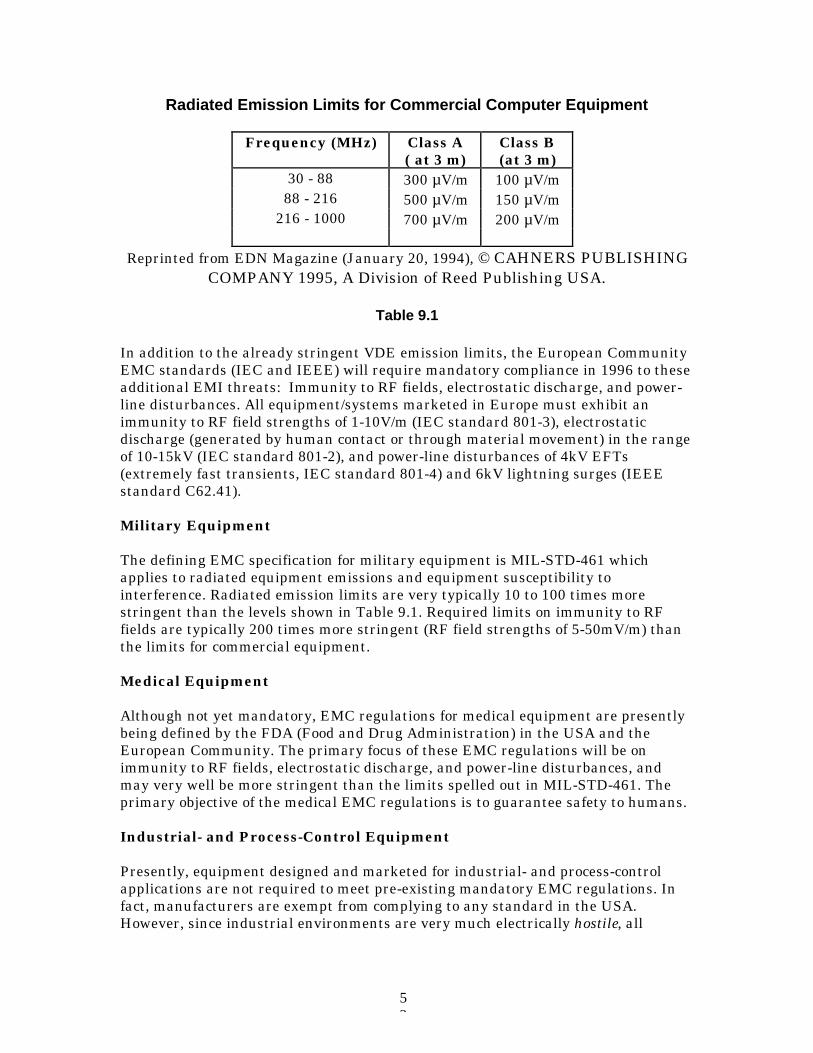
52
Radiated Emission Limits for Commercial Computer Equipment
Frequency (MHz) Class A( at 3 m)
Class B(at 3 m)
30 - 88 300 µV/m 100 µV/m88 - 216 500 µV/m 150 µV/m
216 - 1000 700 µV/m 200 µV/m
Reprinted from EDN Magazine (January 20, 1994), © CAHNERS PUBLISHINGCOMPANY 1995, A Division of Reed Publishing USA.
Table 9.1
In addition to the already stringent VDE emission limits, the European CommunityEMC standards (IEC and IEEE) will require mandatory compliance in 1996 to theseadditional EMI threats: Immunity to RF fields, electrostatic discharge, and power-line disturbances. All equipment/systems marketed in Europe must exhibit animmunity to RF field strengths of 1-10V/m (IEC standard 801-3), electrostaticdischarge (generated by human contact or through material movement) in the rangeof 10-15kV (IEC standard 801-2), and power-line disturbances of 4kV EFTs(extremely fast transients, IEC standard 801-4) and 6kV lightning surges (IEEEstandard C62.41).
Military Equipment
The defining EMC specification for military equipment is MIL-STD-461 whichapplies to radiated equipment emissions and equipment susceptibility tointerference. Radiated emission limits are very typically 10 to 100 times morestringent than the levels shown in Table 9.1. Required limits on immunity to RFfields are typically 200 times more stringent (RF field strengths of 5-50mV/m) thanthe limits for commercial equipment.
Medical Equipment
Although not yet mandatory, EMC regulations for medical equipment are presentlybeing defined by the FDA (Food and Drug Administration) in the USA and theEuropean Community. The primary focus of these EMC regulations will be onimmunity to RF fields, electrostatic discharge, and power-line disturbances, andmay very well be more stringent than the limits spelled out in MIL-STD-461. Theprimary objective of the medical EMC regulations is to guarantee safety to humans.
Industrial- and Process-Control Equipment
Presently, equipment designed and marketed for industrial- and process-controlapplications are not required to meet pre-existing mandatory EMC regulations. Infact, manufacturers are exempt from complying to any standard in the USA.However, since industrial environments are very much electrically hostile, all
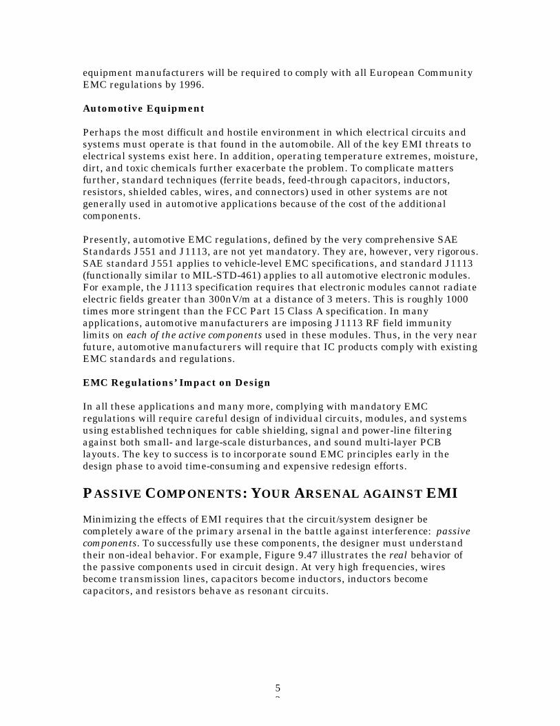
53
equipment manufacturers will be required to comply with all European CommunityEMC regulations by 1996.
Automotive Equipment
Perhaps the most difficult and hostile environment in which electrical circuits andsystems must operate is that found in the automobile. All of the key EMI threats toelectrical systems exist here. In addition, operating temperature extremes, moisture,dirt, and toxic chemicals further exacerbate the problem. To complicate mattersfurther, standard techniques (ferrite beads, feed-through capacitors, inductors,resistors, shielded cables, wires, and connectors) used in other systems are notgenerally used in automotive applications because of the cost of the additionalcomponents.
Presently, automotive EMC regulations, defined by the very comprehensive SAEStandards J551 and J1113, are not yet mandatory. They are, however, very rigorous.SAE standard J551 applies to vehicle-level EMC specifications, and standard J1113(functionally similar to MIL-STD-461) applies to all automotive electronic modules.For example, the J1113 specification requires that electronic modules cannot radiateelectric fields greater than 300nV/m at a distance of 3 meters. This is roughly 1000times more stringent than the FCC Part 15 Class A specification. In manyapplications, automotive manufacturers are imposing J1113 RF field immunitylimits on each of the active components used in these modules. Thus, in the very nearfuture, automotive manufacturers will require that IC products comply with existingEMC standards and regulations.
EMC Regulations’ Impact on Design
In all these applications and many more, complying with mandatory EMCregulations will require careful design of individual circuits, modules, and systemsusing established techniques for cable shielding, signal and power-line filteringagainst both small- and large-scale disturbances, and sound multi-layer PCBlayouts. The key to success is to incorporate sound EMC principles early in thedesign phase to avoid time-consuming and expensive redesign efforts.
PASSIVE COMPONENTS: YOUR ARSENAL AGAINST EMI
Minimizing the effects of EMI requires that the circuit/system designer becompletely aware of the primary arsenal in the battle against interference: passivecomponents. To successfully use these components, the designer must understandtheir non-ideal behavior. For example, Figure 9.47 illustrates the real behavior ofthe passive components used in circuit design. At very high frequencies, wiresbecome transmission lines, capacitors become inductors, inductors becomecapacitors, and resistors behave as resonant circuits.
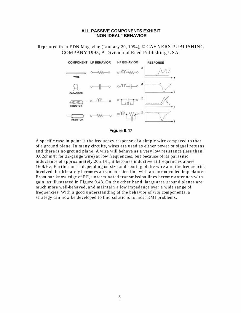
54
ALL PASSIVE COMPONENTS EXHIBIT“NON IDEAL” BEHAVIOR
Reprinted from EDN Magazine (January 20, 1994), © CAHNERS PUBLISHINGCOMPANY 1995, A Division of Reed Publishing USA.
Figure 9.47
A specific case in point is the frequency response of a simple wire compared to thatof a ground plane. In many circuits, wires are used as either power or signal returns,and there is no ground plane. A wire will behave as a very low resistance (less than0.02ohm/ft for 22-gauge wire) at low frequencies, but because of its parasiticinductance of approximately 20nH/ft, it becomes inductive at frequencies above160kHz. Furthermore, depending on size and routing of the wire and the frequenciesinvolved, it ultimately becomes a transmission line with an uncontrolled impedance.From our knowledge of RF, unterminated transmission lines become antennas withgain, as illustrated in Figure 9.48. On the other hand, large area ground planes aremuch more well-behaved, and maintain a low impedance over a wide range offrequencies. With a good understanding of the behavior of real components, astrategy can now be developed to find solutions to most EMI problems.
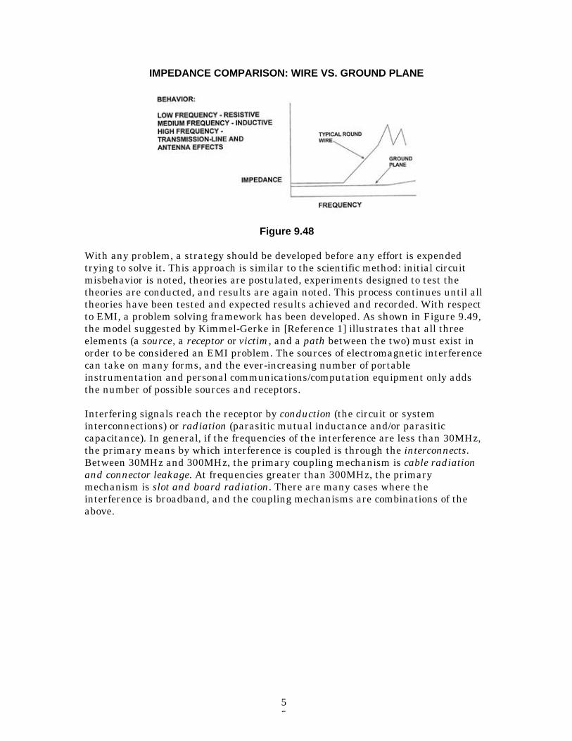
55
IMPEDANCE COMPARISON: WIRE VS. GROUND PLANE
Figure 9.48
With any problem, a strategy should be developed before any effort is expendedtrying to solve it. This approach is similar to the scientific method: initial circuitmisbehavior is noted, theories are postulated, experiments designed to test thetheories are conducted, and results are again noted. This process continues until alltheories have been tested and expected results achieved and recorded. With respectto EMI, a problem solving framework has been developed. As shown in Figure 9.49,the model suggested by Kimmel-Gerke in [Reference 1] illustrates that all threeelements (a source, a receptor or victim, and a path between the two) must exist inorder to be considered an EMI problem. The sources of electromagnetic interferencecan take on many forms, and the ever-increasing number of portableinstrumentation and personal communications/computation equipment only addsthe number of possible sources and receptors.
Interfering signals reach the receptor by conduction (the circuit or systeminterconnections) or radiation (parasitic mutual inductance and/or parasiticcapacitance). In general, if the frequencies of the interference are less than 30MHz,the primary means by which interference is coupled is through the interconnects.Between 30MHz and 300MHz, the primary coupling mechanism is cable radiationand connector leakage. At frequencies greater than 300MHz, the primarymechanism is slot and board radiation. There are many cases where theinterference is broadband, and the coupling mechanisms are combinations of theabove.
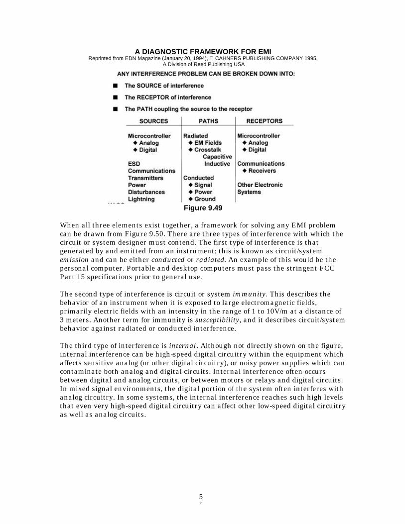
56
A DIAGNOSTIC FRAMEWORK FOR EMIReprinted from EDN Magazine (January 20, 1994), CAHNERS PUBLISHING COMPANY 1995,
A Division of Reed Publishing USA
Figure 9.49
When all three elements exist together, a framework for solving any EMI problemcan be drawn from Figure 9.50. There are three types of interference with which thecircuit or system designer must contend. The first type of interference is thatgenerated by and emitted from an instrument; this is known as circuit/systememission and can be either conducted or radiated. An example of this would be thepersonal computer. Portable and desktop computers must pass the stringent FCCPart 15 specifications prior to general use.
The second type of interference is circuit or system immunity. This describes thebehavior of an instrument when it is exposed to large electromagnetic fields,primarily electric fields with an intensity in the range of 1 to 10V/m at a distance of3 meters. Another term for immunity is susceptibility, and it describes circuit/systembehavior against radiated or conducted interference.
The third type of interference is internal. Although not directly shown on the figure,internal interference can be high-speed digital circuitry within the equipment whichaffects sensitive analog (or other digital circuitry), or noisy power supplies which cancontaminate both analog and digital circuits. Internal interference often occursbetween digital and analog circuits, or between motors or relays and digital circuits.In mixed signal environments, the digital portion of the system often interferes withanalog circuitry. In some systems, the internal interference reaches such high levelsthat even very high-speed digital circuitry can affect other low-speed digital circuitryas well as analog circuits.
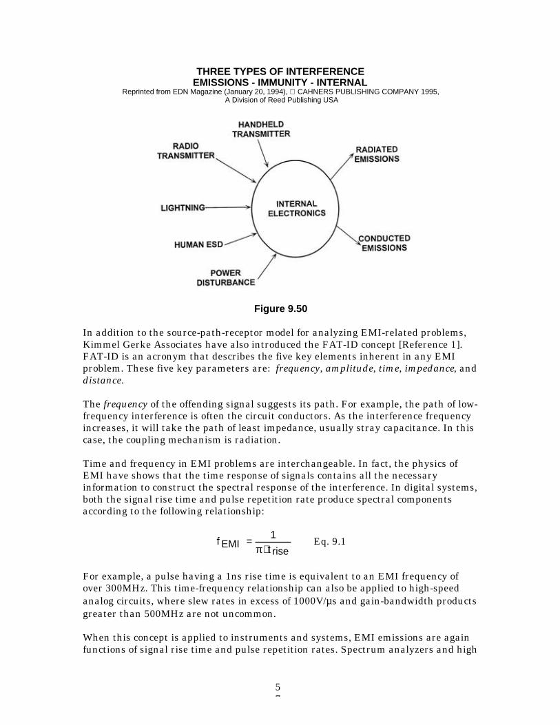
57
THREE TYPES OF INTERFERENCEEMISSIONS - IMMUNITY - INTERNAL
Reprinted from EDN Magazine (January 20, 1994), CAHNERS PUBLISHING COMPANY 1995, A Division of Reed Publishing USA
Figure 9.50
In addition to the source-path-receptor model for analyzing EMI-related problems,Kimmel Gerke Associates have also introduced the FAT-ID concept [Reference 1].FAT-ID is an acronym that describes the five key elements inherent in any EMIproblem. These five key parameters are: frequency, amplitude, time, impedance, anddistance.
The frequency of the offending signal suggests its path. For example, the path of low-frequency interference is often the circuit conductors. As the interference frequencyincreases, it will take the path of least impedance, usually stray capacitance. In thiscase, the coupling mechanism is radiation.
Time and frequency in EMI problems are interchangeable. In fact, the physics ofEMI have shows that the time response of signals contains all the necessaryinformation to construct the spectral response of the interference. In digital systems,both the signal rise time and pulse repetition rate produce spectral componentsaccording to the following relationship:
f EMI1t rise
=⋅π
Eq. 9.1
For example, a pulse having a 1ns rise time is equivalent to an EMI frequency ofover 300MHz. This time-frequency relationship can also be applied to high-speedanalog circuits, where slew rates in excess of 1000V/µs and gain-bandwidth productsgreater than 500MHz are not uncommon.
When this concept is applied to instruments and systems, EMI emissions are againfunctions of signal rise time and pulse repetition rates. Spectrum analyzers and high
58
speed oscilloscopes used with voltage and current probes are very useful tools inquantifying the effects of EMI on circuits and systems.
Another important parameter in the analysis of EMI problems is the physicaldimensions of cables, wires, and enclosures. Cables can behave as either passiveantennas (receptors) or very efficient transmitters (sources) of interference. Theirphysical length and their shield must be carefully examined where EMI is a concern.As previously mentioned, the behavior of simple conductors is a function of length,cross-sectional area, and frequency. Openings in equipment enclosures can behaveas slot antennas, thereby allowing EMI energy to affect the internal electronics.
Radio Frequency Interference
The world is rich in radio transmitters: radio and TV stations, mobile radios,computers, electric motors, garage door openers, electric jackhammers, andcountless others. All this electrical activity can affect circuit/system performanceand, in extreme cases, may render it inoperable. Regardless of the location andmagnitude of the interference, circuits/systems must have a minimum level ofimmunity to radio frequency interference (RFI). The next section will cover twogeneral means by which RFI can disrupt normal instrument operation: the directeffects of RFI sensitive analog circuits, and the effects of RFI on shielded cables.
Two terms are typically used in describing the sensitivity of an electronic system toRF fields. In communications, radio engineers define immunity to be aninstrument’s susceptibility to the applied RFI power density at the unit. In moregeneral EMI analysis, the electric-field intensity is used to describe RFI stimulus.For comparative purposes, Equation 9.2 can be used to convert electric-fieldintensity to power density and vice-versa:
E V
m61.4 PT
mW
cm2
=
Eq. 9.2
where E = Electric Field Strength, in volts per meter, andPT = Transmitted power, in milliwatts per cm^2.
59
From the standpoint of the source-path-receptor model, the strength of the electricfield, E, surrounding the receptor is a function of transmitted power, antenna gain,and distance from the source of the disturbance. An approximation for the electric-field intensity (for both near- and far-field sources) in these terms is given byEquation 9.3:
E V
m 5.5
PT
=⋅
GAd
Eq. 9.3
where E = Electric field intensity, in V/m;PT = Transmitted power, in mW/cm^2;GA = Antenna gain (numerical); andd = distance from source, in meters
For example, a 1W hand-held radio at a distance of 1 meter can generate an electric-field of 5.5V/m, whereas a 10kW radio transmission station located 1km awaygenerates a field smaller than 0.6V/m.
Analog circuits are generally more sensitive to RF fields than digital circuits becauseanalog circuits, operating at high gains, must be able to resolve signals in themicrovolt/millivolt region. Digital circuits, on the other hand, are more immune toRF fields because of their larger signal swings and noise margins. As shown inFigure 9.51, RF fields can use inductive and/or capacitive coupling paths to generatenoise currents and voltages which are amplified by high-impedance analoginstrumentation. In many cases, out-of-band noise signals are detected and rectifiedby these circuits. The result of the RFI rectification is usually unexplained offsetvoltage shifts in the circuit or in the system.
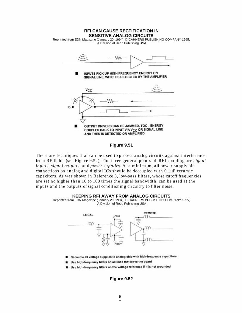
60
RFI CAN CAUSE RECTIFICATION INSENSITIVE ANALOG CIRCUITS
Reprinted from EDN Magazine (January 20, 1994), CAHNERS PUBLISHING COMPANY 1995, A Division of Reed Publishing USA
Figure 9.51
There are techniques that can be used to protect analog circuits against interferencefrom RF fields (see Figure 9.52). The three general points of RFI coupling are signalinputs, signal outputs, and power supplies. At a minimum, all power supply pinconnections on analog and digital ICs should be decoupled with 0.1µF ceramiccapacitors. As was shown in Reference 3, low-pass filters, whose cutoff frequenciesare set no higher than 10 to 100 times the signal bandwidth, can be used at theinputs and the outputs of signal conditioning circuitry to filter noise.
KEEPING RFI AWAY FROM ANALOG CIRCUITSReprinted from EDN Magazine (January 20, 1994), CAHNERS PUBLISHING COMPANY 1995,
A Division of Reed Publishing USA
Figure 9.52
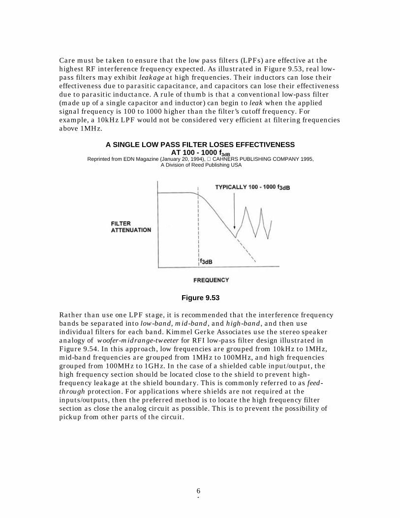
61
Care must be taken to ensure that the low pass filters (LPFs) are effective at thehighest RF interference frequency expected. As illustrated in Figure 9.53, real low-pass filters may exhibit leakage at high frequencies. Their inductors can lose theireffectiveness due to parasitic capacitance, and capacitors can lose their effectivenessdue to parasitic inductance. A rule of thumb is that a conventional low-pass filter(made up of a single capacitor and inductor) can begin to leak when the appliedsignal frequency is 100 to 1000 higher than the filter’s cutoff frequency. Forexample, a 10kHz LPF would not be considered very efficient at filtering frequenciesabove 1MHz.
A SINGLE LOW PASS FILTER LOSES EFFECTIVENESSAT 100 - 1000 f3dB
Reprinted from EDN Magazine (January 20, 1994), CAHNERS PUBLISHING COMPANY 1995, A Division of Reed Publishing USA
Figure 9.53
Rather than use one LPF stage, it is recommended that the interference frequencybands be separated into low-band, mid-band, and high-band, and then useindividual filters for each band. Kimmel Gerke Associates use the stereo speakeranalogy of woofer-midrange-tweeter for RFI low-pass filter design illustrated inFigure 9.54. In this approach, low frequencies are grouped from 10kHz to 1MHz,mid-band frequencies are grouped from 1MHz to 100MHz, and high frequenciesgrouped from 100MHz to 1GHz. In the case of a shielded cable input/output, thehigh frequency section should be located close to the shield to prevent high-frequency leakage at the shield boundary. This is commonly referred to as feed-through protection. For applications where shields are not required at theinputs/outputs, then the preferred method is to locate the high frequency filtersection as close the analog circuit as possible. This is to prevent the possibility ofpickup from other parts of the circuit.
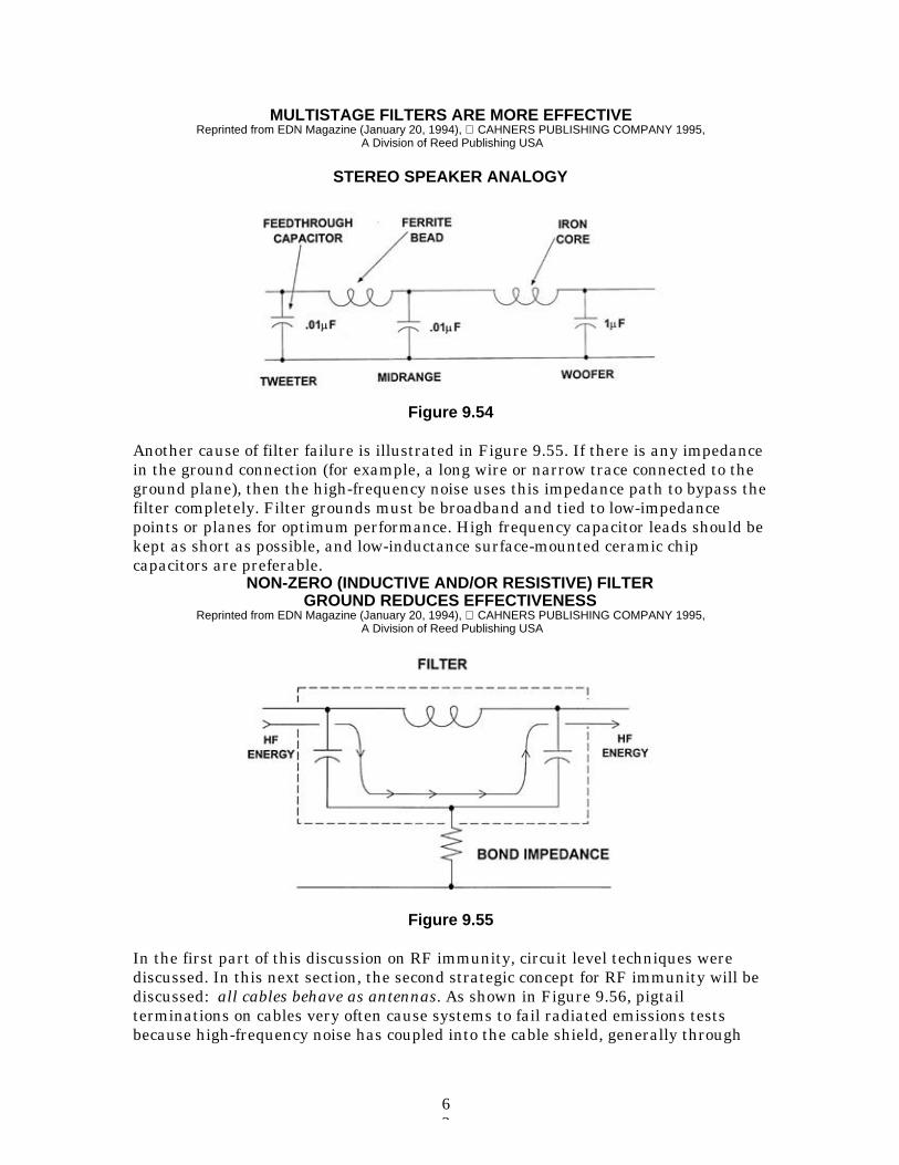
62
MULTISTAGE FILTERS ARE MORE EFFECTIVEReprinted from EDN Magazine (January 20, 1994), CAHNERS PUBLISHING COMPANY 1995,
A Division of Reed Publishing USA
STEREO SPEAKER ANALOGY
Figure 9.54
Another cause of filter failure is illustrated in Figure 9.55. If there is any impedancein the ground connection (for example, a long wire or narrow trace connected to theground plane), then the high-frequency noise uses this impedance path to bypass thefilter completely. Filter grounds must be broadband and tied to low-impedancepoints or planes for optimum performance. High frequency capacitor leads should bekept as short as possible, and low-inductance surface-mounted ceramic chipcapacitors are preferable.
NON-ZERO (INDUCTIVE AND/OR RESISTIVE) FILTERGROUND REDUCES EFFECTIVENESS
Reprinted from EDN Magazine (January 20, 1994), CAHNERS PUBLISHING COMPANY 1995, A Division of Reed Publishing USA
Figure 9.55
In the first part of this discussion on RF immunity, circuit level techniques werediscussed. In this next section, the second strategic concept for RF immunity will bediscussed: all cables behave as antennas. As shown in Figure 9.56, pigtailterminations on cables very often cause systems to fail radiated emissions testsbecause high-frequency noise has coupled into the cable shield, generally through
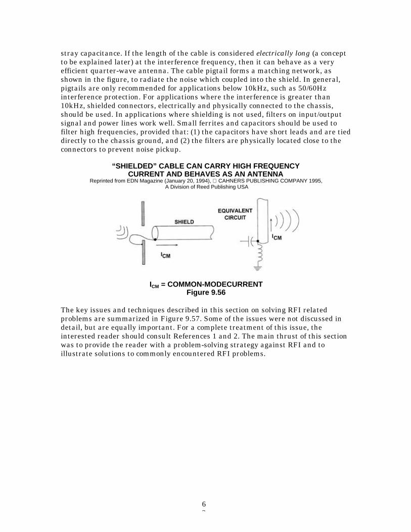
63
stray capacitance. If the length of the cable is considered electrically long (a conceptto be explained later) at the interference frequency, then it can behave as a veryefficient quarter-wave antenna. The cable pigtail forms a matching network, asshown in the figure, to radiate the noise which coupled into the shield. In general,pigtails are only recommended for applications below 10kHz, such as 50/60Hzinterference protection. For applications where the interference is greater than10kHz, shielded connectors, electrically and physically connected to the chassis,should be used. In applications where shielding is not used, filters on input/outputsignal and power lines work well. Small ferrites and capacitors should be used tofilter high frequencies, provided that: (1) the capacitors have short leads and are tieddirectly to the chassis ground, and (2) the filters are physically located close to theconnectors to prevent noise pickup.
“SHIELDED” CABLE CAN CARRY HIGH FREQUENCYCURRENT AND BEHAVES AS AN ANTENNA
Reprinted from EDN Magazine (January 20, 1994), CAHNERS PUBLISHING COMPANY 1995, A Division of Reed Publishing USA
ICM = COMMON-MODECURRENTFigure 9.56
The key issues and techniques described in this section on solving RFI relatedproblems are summarized in Figure 9.57. Some of the issues were not discussed indetail, but are equally important. For a complete treatment of this issue, theinterested reader should consult References 1 and 2. The main thrust of this sectionwas to provide the reader with a problem-solving strategy against RFI and toillustrate solutions to commonly encountered RFI problems.
64
SUMMARY OF RADIO FREQUENCY INTERFERENCEAND PROTECTION TECHNIQUES
Reprinted from EDN Magazine (January 20, 1994), CAHNERS PUBLISHING COMPANY 1995, A Division of Reed Publishing USA
Radio-Frequency Interference is a Serious ThreatEquipment causes interference to nearby radio andtelevisonEquipment upset by nearby transmitters
RF-Failure ModesDigital circuits prime source of emissionsAnalog circuits more vulnerable to RF than digital circuits
Two Strategic ConceptsTreat all cables as antennasDetermine the most critical circuits
RF Circuit ProtectionFilters and multilayer boardsMultistage filters often needed
RF ShieldingSlots and seams cause the most problems
RF Cable ProtectionHigh-quality shields and connectors needed for RFprotection
Figure 9.57
Solutions for Power-Line Disturbances
The goal of this next section is not to describe in detail all the circuit/system failuremechanisms which can result from power-line disturbances or faults. Nor is it theintent of this section to describe methods by which power-line disturbances can beprevented. Instead, this section will describe techniques that allow circuits andsystems to accommodate transient power-line disturbances.
Figure 9.58 is an example of a hybrid power transient protection network commonlyused in many applications where lightning transients or other power-linedisturbances are prevalent. These networks can be designed to provide protectionagainst transients as high as 10kV and as fast as 10ns. Gas discharge tubes(crowbars) and large geometry zener diodes (clamps) are used to provide bothdifferential and common-mode protection. Metal-oxide varistors (MOVs) can besubstituted for the zener diodes in less critical, or in more compact designs. Chokesare used to limit the surge current until the gas discharge tubes fire.
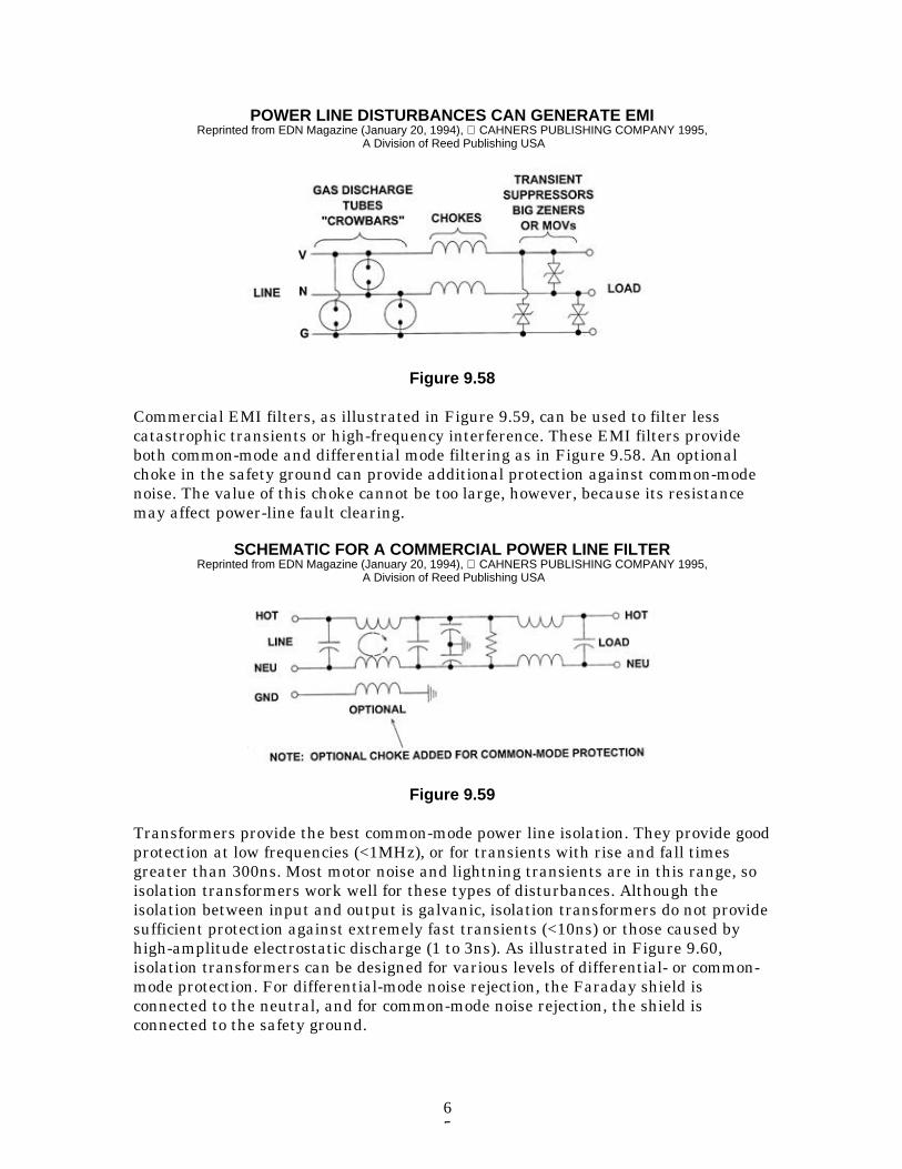
65
POWER LINE DISTURBANCES CAN GENERATE EMIReprinted from EDN Magazine (January 20, 1994), CAHNERS PUBLISHING COMPANY 1995,
A Division of Reed Publishing USA
Figure 9.58
Commercial EMI filters, as illustrated in Figure 9.59, can be used to filter lesscatastrophic transients or high-frequency interference. These EMI filters provideboth common-mode and differential mode filtering as in Figure 9.58. An optionalchoke in the safety ground can provide additional protection against common-modenoise. The value of this choke cannot be too large, however, because its resistancemay affect power-line fault clearing.
SCHEMATIC FOR A COMMERCIAL POWER LINE FILTERReprinted from EDN Magazine (January 20, 1994), CAHNERS PUBLISHING COMPANY 1995,
A Division of Reed Publishing USA
Figure 9.59
Transformers provide the best common-mode power line isolation. They provide goodprotection at low frequencies (<1MHz), or for transients with rise and fall timesgreater than 300ns. Most motor noise and lightning transients are in this range, soisolation transformers work well for these types of disturbances. Although theisolation between input and output is galvanic, isolation transformers do not providesufficient protection against extremely fast transients (<10ns) or those caused byhigh-amplitude electrostatic discharge (1 to 3ns). As illustrated in Figure 9.60,isolation transformers can be designed for various levels of differential- or common-mode protection. For differential-mode noise rejection, the Faraday shield isconnected to the neutral, and for common-mode noise rejection, the shield isconnected to the safety ground.
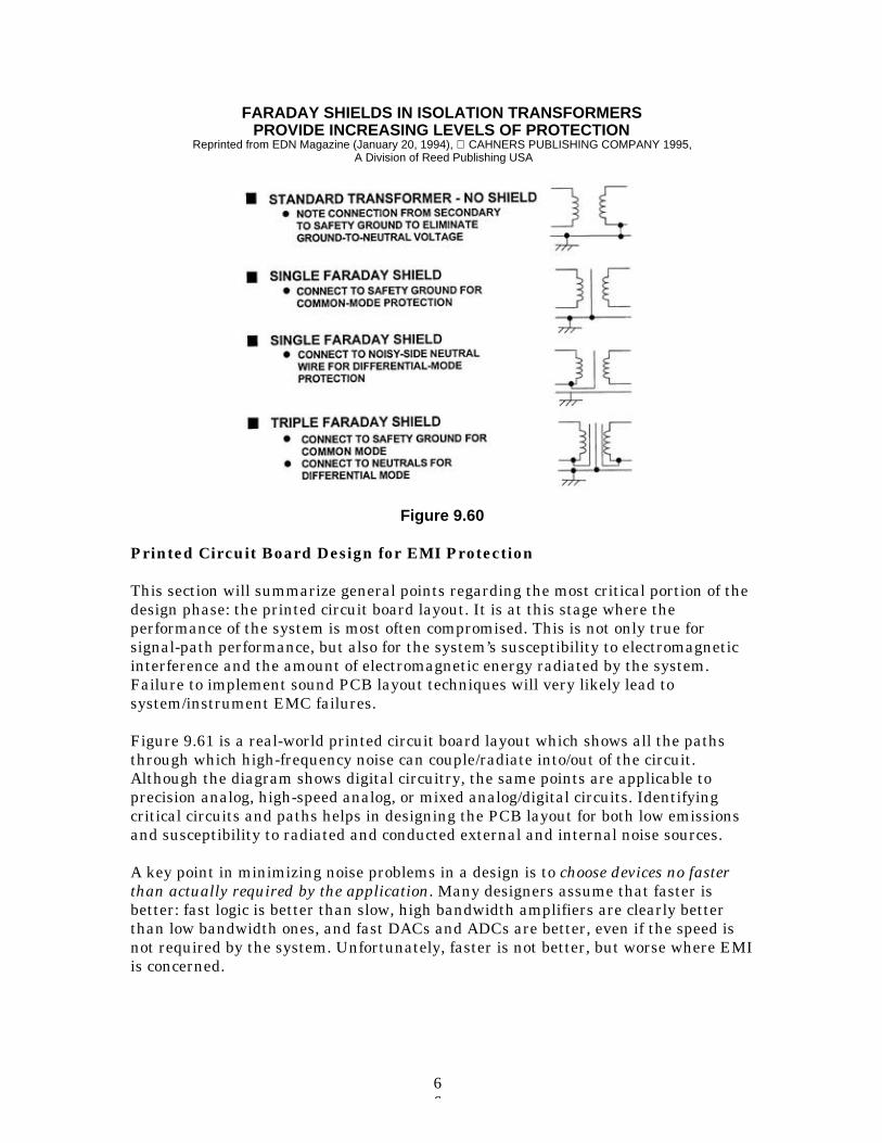
66
FARADAY SHIELDS IN ISOLATION TRANSFORMERSPROVIDE INCREASING LEVELS OF PROTECTION
Reprinted from EDN Magazine (January 20, 1994), CAHNERS PUBLISHING COMPANY 1995, A Division of Reed Publishing USA
Figure 9.60
Printed Circuit Board Design for EMI Protection
This section will summarize general points regarding the most critical portion of thedesign phase: the printed circuit board layout. It is at this stage where theperformance of the system is most often compromised. This is not only true forsignal-path performance, but also for the system’s susceptibility to electromagneticinterference and the amount of electromagnetic energy radiated by the system.Failure to implement sound PCB layout techniques will very likely lead tosystem/instrument EMC failures.
Figure 9.61 is a real-world printed circuit board layout which shows all the pathsthrough which high-frequency noise can couple/radiate into/out of the circuit.Although the diagram shows digital circuitry, the same points are applicable toprecision analog, high-speed analog, or mixed analog/digital circuits. Identifyingcritical circuits and paths helps in designing the PCB layout for both low emissionsand susceptibility to radiated and conducted external and internal noise sources.
A key point in minimizing noise problems in a design is to choose devices no fasterthan actually required by the application. Many designers assume that faster isbetter: fast logic is better than slow, high bandwidth amplifiers are clearly betterthan low bandwidth ones, and fast DACs and ADCs are better, even if the speed isnot required by the system. Unfortunately, faster is not better, but worse where EMIis concerned.
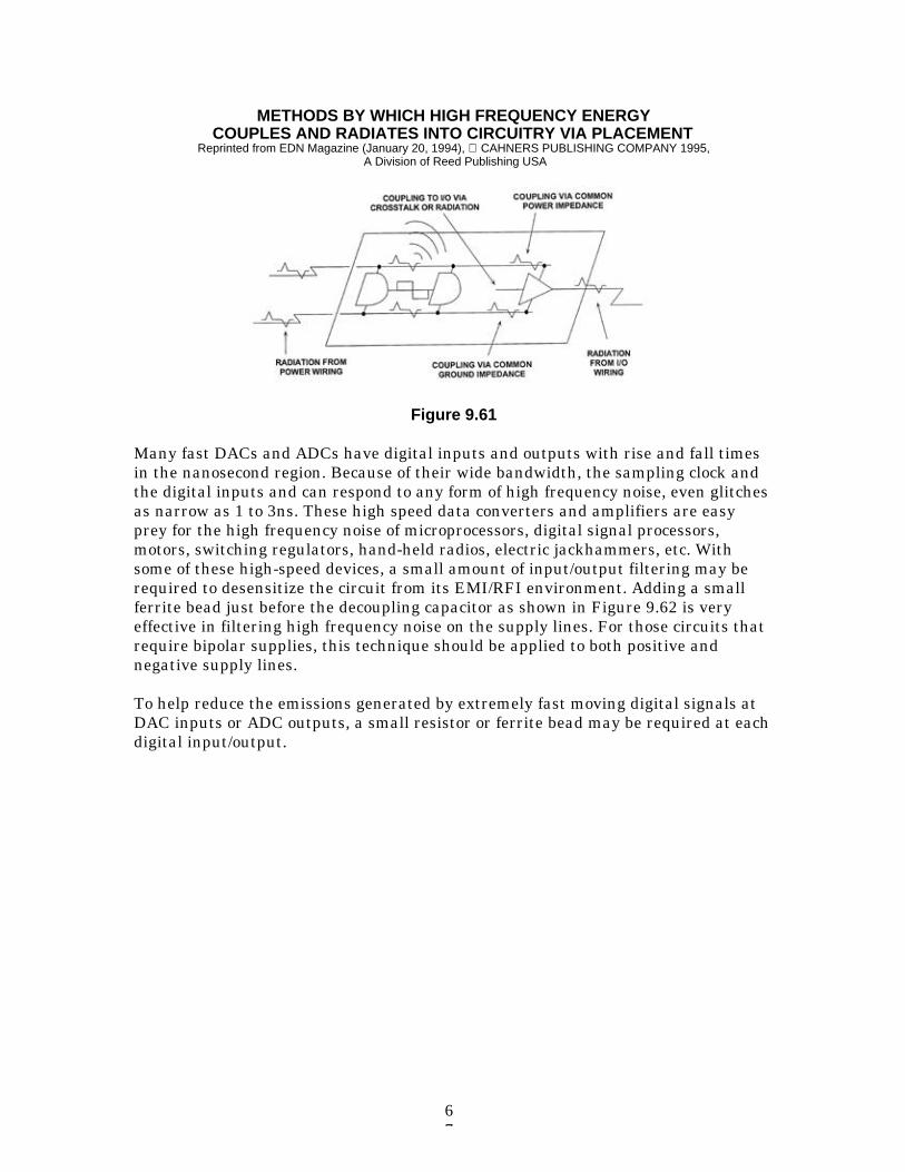
67
METHODS BY WHICH HIGH FREQUENCY ENERGYCOUPLES AND RADIATES INTO CIRCUITRY VIA PLACEMENT
Reprinted from EDN Magazine (January 20, 1994), CAHNERS PUBLISHING COMPANY 1995, A Division of Reed Publishing USA
Figure 9.61
Many fast DACs and ADCs have digital inputs and outputs with rise and fall timesin the nanosecond region. Because of their wide bandwidth, the sampling clock andthe digital inputs and can respond to any form of high frequency noise, even glitchesas narrow as 1 to 3ns. These high speed data converters and amplifiers are easyprey for the high frequency noise of microprocessors, digital signal processors,motors, switching regulators, hand-held radios, electric jackhammers, etc. Withsome of these high-speed devices, a small amount of input/output filtering may berequired to desensitize the circuit from its EMI/RFI environment. Adding a smallferrite bead just before the decoupling capacitor as shown in Figure 9.62 is veryeffective in filtering high frequency noise on the supply lines. For those circuits thatrequire bipolar supplies, this technique should be applied to both positive andnegative supply lines.
To help reduce the emissions generated by extremely fast moving digital signals atDAC inputs or ADC outputs, a small resistor or ferrite bead may be required at eachdigital input/output.
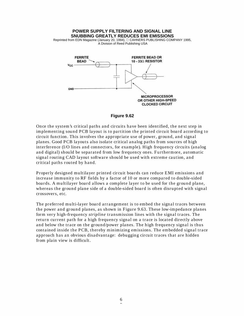
68
POWER SUPPLY FILTERING AND SIGNAL LINESNUBBING GREATLY REDUCES EMI EMISSIONS
Reprinted from EDN Magazine (January 20, 1994), CAHNERS PUBLISHING COMPANY 1995, A Division of Reed Publishing USA
Figure 9.62
Once the system’s critical paths and circuits have been identified, the next step inimplementing sound PCB layout is to partition the printed circuit board according tocircuit function. This involves the appropriate use of power, ground, and signalplanes. Good PCB layouts also isolate critical analog paths from sources of highinterference (I/O lines and connectors, for example). High frequency circuits (analogand digital) should be separated from low frequency ones. Furthermore, automaticsignal routing CAD layout software should be used with extreme caution, andcritical paths routed by hand.
Properly designed multilayer printed circuit boards can reduce EMI emissions andincrease immunity to RF fields by a factor of 10 or more compared to double-sidedboards. A multilayer board allows a complete layer to be used for the ground plane,whereas the ground plane side of a double-sided board is often disrupted with signalcrossovers, etc.
The preferred multi-layer board arrangement is to embed the signal traces betweenthe power and ground planes, as shown in Figure 9.63. These low-impedance planesform very high-frequency stripline transmission lines with the signal traces. Thereturn current path for a high frequency signal on a trace is located directly aboveand below the trace on the ground/power planes. The high frequency signal is thuscontained inside the PCB, thereby minimizing emissions. The embedded signal traceapproach has an obvious disadvantage: debugging circuit traces that are hiddenfrom plain view is difficult.
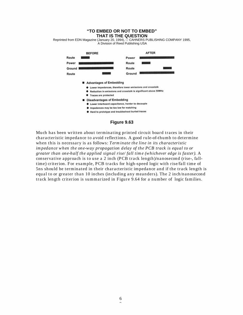
69
“TO EMBED OR NOT TO EMBED”THAT IS THE QUESTION
Reprinted from EDN Magazine (January 20, 1994), CAHNERS PUBLISHING COMPANY 1995, A Division of Reed Publishing USA
Figure 9.63
Much has been written about terminating printed circuit board traces in theircharacteristic impedance to avoid reflections. A good rule-of-thumb to determinewhen this is necessary is as follows: Terminate the line in its characteristicimpedance when the one-way propagation delay of the PCB track is equal to orgreater than one-half the applied signal rise/fall time (whichever edge is faster). Aconservative approach is to use a 2 inch (PCB track length)/nanosecond (rise-, fall-time) criterion. For example, PCB tracks for high-speed logic with rise/fall time of5ns should be terminated in their characteristic impedance and if the track length isequal to or greater than 10 inches (including any meanders). The 2 inch/nanosecondtrack length criterion is summarized in Figure 9.64 for a number of logic families.
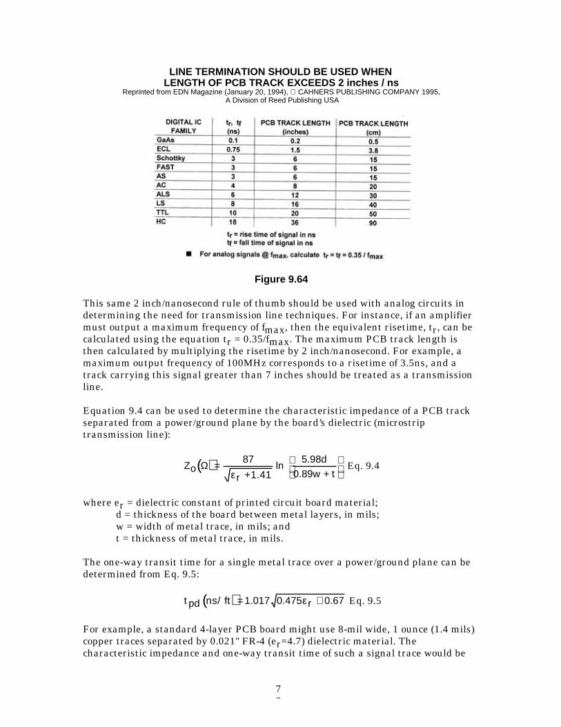
70
LINE TERMINATION SHOULD BE USED WHENLENGTH OF PCB TRACK EXCEEDS 2 inches / ns
Reprinted from EDN Magazine (January 20, 1994), CAHNERS PUBLISHING COMPANY 1995, A Division of Reed Publishing USA
Figure 9.64
This same 2 inch/nanosecond rule of thumb should be used with analog circuits indetermining the need for transmission line techniques. For instance, if an amplifiermust output a maximum frequency of fmax, then the equivalent risetime, tr, can becalculated using the equation tr = 0.35/fmax. The maximum PCB track length isthen calculated by multiplying the risetime by 2 inch/nanosecond. For example, amaximum output frequency of 100MHz corresponds to a risetime of 3.5ns, and atrack carrying this signal greater than 7 inches should be treated as a transmissionline.
Equation 9.4 can be used to determine the characteristic impedance of a PCB trackseparated from a power/ground plane by the board’s dielectric (microstriptransmission line):
( )Zor +1.41
5.98d
0.89w + tΩ =
87
εln Eq. 9.4
where er = dielectric constant of printed circuit board material;d = thickness of the board between metal layers, in mils;w = width of metal trace, in mils; andt = thickness of metal trace, in mils.
The one-way transit time for a single metal trace over a power/ground plane can bedetermined from Eq. 9.5:
( )t pd ns/ ft 1.017 0.475 r 0.67 = +ε Eq. 9.5
For example, a standard 4-layer PCB board might use 8-mil wide, 1 ounce (1.4 mils)copper traces separated by 0.021" FR-4 (er=4.7) dielectric material. Thecharacteristic impedance and one-way transit time of such a signal trace would be
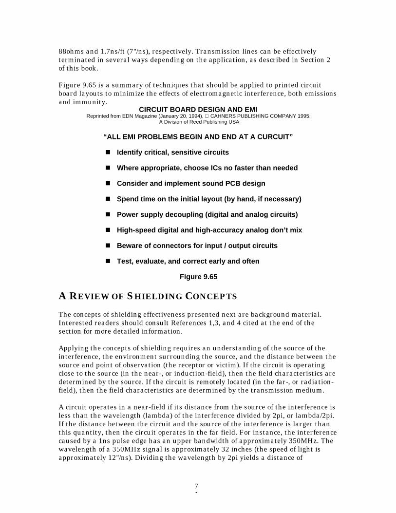
71
88ohms and 1.7ns/ft (7"/ns), respectively. Transmission lines can be effectivelyterminated in several ways depending on the application, as described in Section 2of this book.
Figure 9.65 is a summary of techniques that should be applied to printed circuitboard layouts to minimize the effects of electromagnetic interference, both emissionsand immunity.
CIRCUIT BOARD DESIGN AND EMIReprinted from EDN Magazine (January 20, 1994), CAHNERS PUBLISHING COMPANY 1995,
A Division of Reed Publishing USA
“ALL EMI PROBLEMS BEGIN AND END AT A CURCUIT”
Identify critical, sensitive circuits
Where appropriate, choose ICs no faster than needed
Consider and implement sound PCB design
Spend time on the initial layout (by hand, if necessary)
Power supply decoupling (digital and analog circuits)
High-speed digital and high-accuracy analog don’t mix
Beware of connectors for input / output circuits
Test, evaluate, and correct early and often
Figure 9.65
A REVIEW OF SHIELDING CONCEPTS
The concepts of shielding effectiveness presented next are background material.Interested readers should consult References 1,3, and 4 cited at the end of thesection for more detailed information.
Applying the concepts of shielding requires an understanding of the source of theinterference, the environment surrounding the source, and the distance between thesource and point of observation (the receptor or victim). If the circuit is operatingclose to the source (in the near-, or induction-field), then the field characteristics aredetermined by the source. If the circuit is remotely located (in the far-, or radiation-field), then the field characteristics are determined by the transmission medium.
A circuit operates in a near-field if its distance from the source of the interference isless than the wavelength (lambda) of the interference divided by 2pi, or lambda/2pi.If the distance between the circuit and the source of the interference is larger thanthis quantity, then the circuit operates in the far field. For instance, the interferencecaused by a 1ns pulse edge has an upper bandwidth of approximately 350MHz. Thewavelength of a 350MHz signal is approximately 32 inches (the speed of light isapproximately 12"/ns). Dividing the wavelength by 2pi yields a distance of
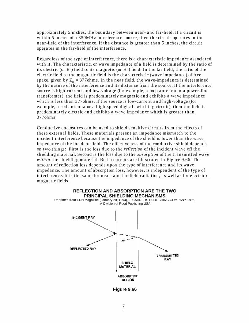
72
approximately 5 inches, the boundary between near- and far-field. If a circuit iswithin 5 inches of a 350MHz interference source, then the circuit operates in thenear-field of the interference. If the distance is greater than 5 inches, the circuitoperates in the far-field of the interference.
Regardless of the type of interference, there is a characteristic impedance associatedwith it. The characteristic, or wave impedance of a field is determined by the ratio ofits electric (or E-) field to its magnetic (or H-) field. In the far field, the ratio of theelectric field to the magnetic field is the characteristic (wave impedance) of freespace, given by Zo = 377ohms. In the near field, the wave-impedance is determinedby the nature of the interference and its distance from the source. If the interferencesource is high-current and low-voltage (for example, a loop antenna or a power-linetransformer), the field is predominately magnetic and exhibits a wave impedancewhich is less than 377ohms. If the source is low-current and high-voltage (forexample, a rod antenna or a high-speed digital switching circuit), then the field ispredominately electric and exhibits a wave impedance which is greater than377ohms.
Conductive enclosures can be used to shield sensitive circuits from the effects ofthese external fields. These materials present an impedance mismatch to theincident interference because the impedance of the shield is lower than the waveimpedance of the incident field. The effectiveness of the conductive shield dependson two things: First is the loss due to the reflection of the incident wave off theshielding material. Second is the loss due to the absorption of the transmitted wavewithin the shielding material. Both concepts are illustrated in Figure 9.66. Theamount of reflection loss depends upon the type of interference and its waveimpedance. The amount of absorption loss, however, is independent of the type ofinterference. It is the same for near- and far-field radiation, as well as for electric ormagnetic fields.
REFLECTION AND ABSORPTION ARE THE TWOPRINCIPAL SHIELDING MECHANISMS
Reprinted from EDN Magazine (January 20, 1994), CAHNERS PUBLISHING COMPANY 1995, A Division of Reed Publishing USA
Figure 9.66
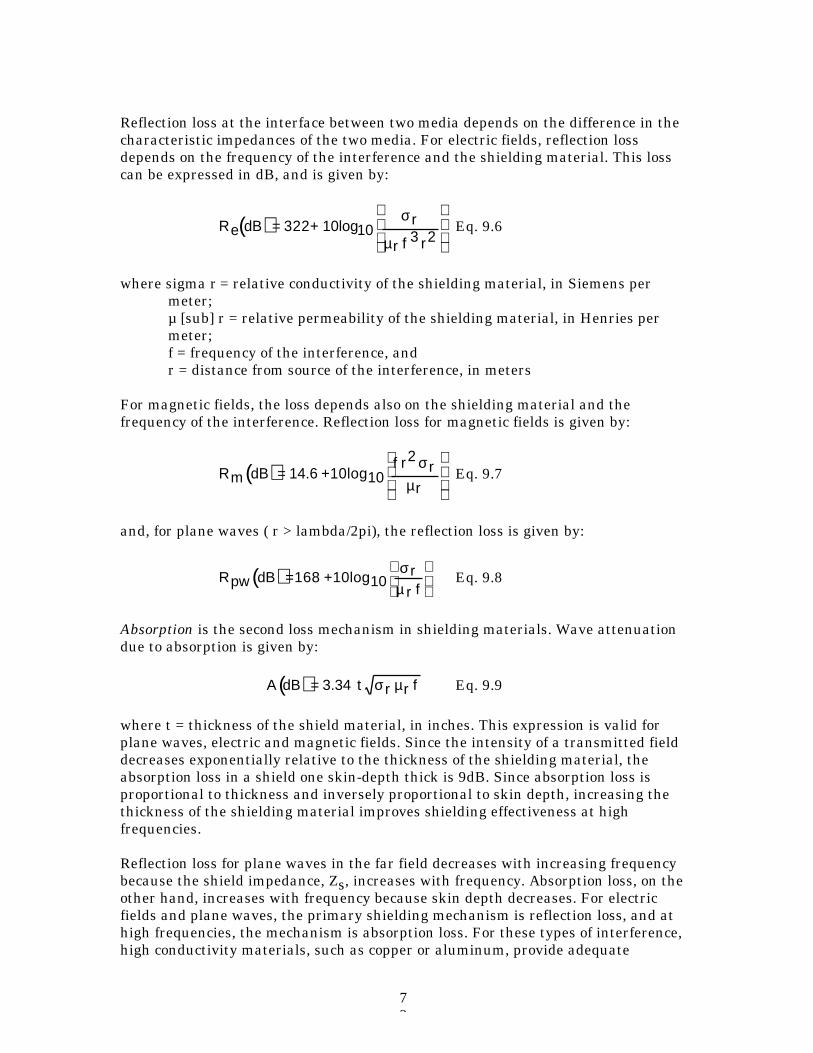
73
Reflection loss at the interface between two media depends on the difference in thecharacteristic impedances of the two media. For electric fields, reflection lossdepends on the frequency of the interference and the shielding material. This losscan be expressed in dB, and is given by:
( )Re dB = 322+ 10log10r
r f 3 r2σ
µ
Eq. 9.6
where sigma r = relative conductivity of the shielding material, in Siemens permeter;µ [sub] r = relative permeability of the shielding material, in Henries permeter;f = frequency of the interference, andr = distance from source of the interference, in meters
For magnetic fields, the loss depends also on the shielding material and thefrequency of the interference. Reflection loss for magnetic fields is given by:
( )Rm dB = 14.6 +10log10f r2
rr
σµ
Eq. 9.7
and, for plane waves ( r > lambda/2pi), the reflection loss is given by:
( )Rpw dB =168 +10log10r
r f
σµ
Eq. 9.8
Absorption is the second loss mechanism in shielding materials. Wave attenuationdue to absorption is given by:
( )A dB = 3.34 t r r fσ µ Eq. 9.9
where t = thickness of the shield material, in inches. This expression is valid forplane waves, electric and magnetic fields. Since the intensity of a transmitted fielddecreases exponentially relative to the thickness of the shielding material, theabsorption loss in a shield one skin-depth thick is 9dB. Since absorption loss isproportional to thickness and inversely proportional to skin depth, increasing thethickness of the shielding material improves shielding effectiveness at highfrequencies.
Reflection loss for plane waves in the far field decreases with increasing frequencybecause the shield impedance, Zs, increases with frequency. Absorption loss, on theother hand, increases with frequency because skin depth decreases. For electricfields and plane waves, the primary shielding mechanism is reflection loss, and athigh frequencies, the mechanism is absorption loss. For these types of interference,high conductivity materials, such as copper or aluminum, provide adequate
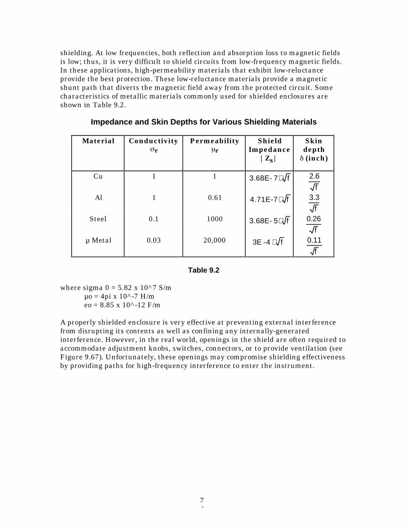
74
shielding. At low frequencies, both reflection and absorption loss to magnetic fieldsis low; thus, it is very difficult to shield circuits from low-frequency magnetic fields.In these applications, high-permeability materials that exhibit low-reluctanceprovide the best protection. These low-reluctance materials provide a magneticshunt path that diverts the magnetic field away from the protected circuit. Somecharacteristics of metallic materials commonly used for shielded enclosures areshown in Table 9.2.
Impedance and Skin Depths for Various Shielding Materials
Material Conductivityr
Permeabilityr
ShieldImpedance
|Zs|
Skindepth (inch)
Cu 1 1 3.68E- 7 f ⋅ 2.6
f
Al 1 0.61 4.71E-7 f ⋅ 3.3
f
Steel 0.1 1000 3.68E- 5 f ⋅ 0.26
f
µ Metal 0.03 20,000 3E -4 f ⋅ 0.11
f
Table 9.2
where sigma 0 = 5.82 x 10^7 S/mµo = 4pi x 10^-7 H/meo = 8.85 x 10^-12 F/m
A properly shielded enclosure is very effective at preventing external interferencefrom disrupting its contents as well as confining any internally-generatedinterference. However, in the real world, openings in the shield are often required toaccommodate adjustment knobs, switches, connectors, or to provide ventilation (seeFigure 9.67). Unfortunately, these openings may compromise shielding effectivenessby providing paths for high-frequency interference to enter the instrument.
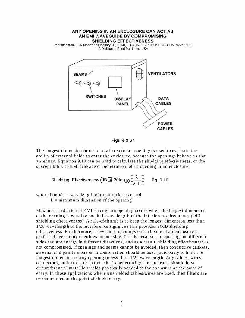
75
ANY OPENING IN AN ENCLOSURE CAN ACT ASAN EMI WAVEGUIDE BY COMPROMISING
SHIELDING EFFECTIVENESSReprinted from EDN Magazine (January 20, 1994), CAHNERS PUBLISHING COMPANY 1995,
A Division of Reed Publishing USA
Figure 9.67
The longest dimension (not the total area) of an opening is used to evaluate theability of external fields to enter the enclosure, because the openings behave as slotantennas. Equation 9.10 can be used to calculate the shielding effectiveness, or thesusceptibility to EMI leakage or penetration, of an opening in an enclosure:
( )Shielding Effectiven ess dB = 20log10 2 Lλ⋅
Eq. 9.10
where lambda = wavelength of the interference andL = maximum dimension of the opening
Maximum radiation of EMI through an opening occurs when the longest dimensionof the opening is equal to one half-wavelength of the interference frequency (0dBshielding effectiveness). A rule-of-thumb is to keep the longest dimension less than1/20 wavelength of the interference signal, as this provides 20dB shieldingeffectiveness. Furthermore, a few small openings on each side of an enclosure ispreferred over many openings on one side. This is because the openings on differentsides radiate energy in different directions, and as a result, shielding effectiveness isnot compromised. If openings and seams cannot be avoided, then conductive gaskets,screens, and paints alone or in combination should be used judiciously to limit thelongest dimension of any opening to less than 1/20 wavelength. Any cables, wires,connectors, indicators, or control shafts penetrating the enclosure should havecircumferential metallic shields physically bonded to the enclosure at the point ofentry. In those applications where unshielded cables/wires are used, then filters arerecommended at the point of shield entry.
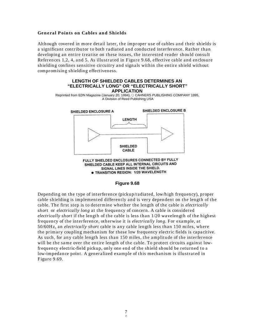
76
General Points on Cables and Shields
Although covered in more detail later, the improper use of cables and their shields isa significant contributor to both radiated and conducted interference. Rather thandeveloping an entire treatise on these issues, the interested reader should consultReferences 1,2, 4, and 5. As illustrated in Figure 9.68, effective cable and enclosureshielding confines sensitive circuitry and signals within the entire shield withoutcompromising shielding effectiveness.
LENGTH OF SHIELDED CABLES DETERMINES AN“ELECTRICALLY LONG” OR “ELECTRICALLY SHORT”
APPLICATIONReprinted from EDN Magazine (January 20, 1994), CAHNERS PUBLISHING COMPANY 1995,
A Division of Reed Publishing USA
Figure 9.68
Depending on the type of interference (pickup/radiated, low/high frequency), propercable shielding is implemented differently and is very dependent on the length of thecable. The first step is to determine whether the length of the cable is electricallyshort or electrically long at the frequency of concern. A cable is consideredelectrically short if the length of the cable is less than 1/20 wavelength of the highestfrequency of the interference, otherwise it is electrically long. For example, at50/60Hz, an electrically short cable is any cable length less than 150 miles, wherethe primary coupling mechanism for these low frequency electric fields is capacitive.As such, for any cable length less than 150 miles, the amplitude of the interferencewill be the same over the entire length of the cable. To protect circuits against low-frequency electric-field pickup, only one end of the shield should be returned to alow-impedance point. A generalized example of this mechanism is illustrated inFigure 9.69.
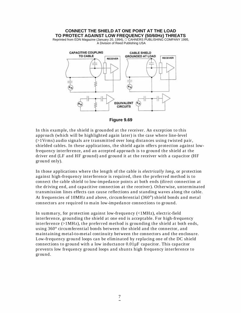
77
CONNECT THE SHIELD AT ONE POINT AT THE LOADTO PROTECT AGAINST LOW FREQUENCY (50/60Hz) THREATS
Reprinted from EDN Magazine (January 20, 1994), CAHNERS PUBLISHING COMPANY 1995, A Division of Reed Publishing USA
Figure 9.69
In this example, the shield is grounded at the receiver. An exception to thisapproach (which will be highlighted again later) is the case where line-level(>1Vrms) audio signals are transmitted over long distances using twisted pair,shielded cables. In these applications, the shield again offers protection against low-frequency interference, and an accepted approach is to ground the shield at thedriver end (LF and HF ground) and ground it at the receiver with a capacitor (HFground only).
In those applications where the length of the cable is electrically long, or protectionagainst high-frequency interference is required, then the preferred method is toconnect the cable shield to low-impedance points at both ends (direct connection atthe driving end, and capacitive connection at the receiver). Otherwise, unterminatedtransmission lines effects can cause reflections and standing waves along the cable.At frequencies of 10MHz and above, circumferential (360°) shield bonds and metalconnectors are required to main low-impedance connections to ground.
In summary, for protection against low-frequency (<1MHz), electric-fieldinterference, grounding the shield at one end is acceptable. For high-frequencyinterference (>1MHz), the preferred method is grounding the shield at both ends,using 360° circumferential bonds between the shield and the connector, andmaintaining metal-to-metal continuity between the connectors and the enclosure.Low-frequency ground loops can be eliminated by replacing one of the DC shieldconnections to ground with a low inductance 0.01µF capacitor. This capacitorprevents low frequency ground loops and shunts high frequency interference toground.
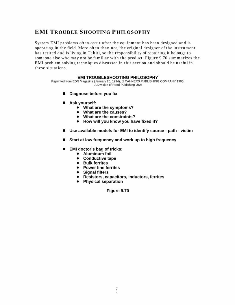
78
EMI TROUBLE SHOOTING PHILOSOPHY
System EMI problems often occur after the equipment has been designed and isoperating in the field. More often than not, the original designer of the instrumenthas retired and is living in Tahiti, so the responsibility of repairing it belongs tosomeone else who may not be familiar with the product. Figure 9.70 summarizes theEMI problem solving techniques discussed in this section and should be useful inthese situations.
EMI TROUBLESHOOTING PHILOSOPHYReprinted from EDN Magazine (January 20, 1994), CAHNERS PUBLISHING COMPANY 1995,
A Division of Reed Publishing USA
Diagnose before you fix
Ask yourself:What are the symptoms?What are the causes?What are the constraints?How will you know you have fixed it?
Use available models for EMI to identify source - path - victim
Start at low frequency and work up to high frequency
EMI doctor’s bag of tricks:Aluminum foilConductive tapeBulk ferritesPower line ferritesSignal filtersResistors, capacitors, inductors, ferritesPhysical separation
Figure 9.70
79
REFERENCES ON EMI/RFI
1. EDN’s Designer’s Guide to Electromagnetic Compatibility, EDN,January, 20, 1994, material reprinted by permission of Cahners Publishing Company, 1995.
2. Designing for EMC (Workshop Notes), Kimmel Gerke Associates, Ltd., 1994.
3. Systems Application Guide, Chapter 1, pg. 21-55, Analog Devices,Incorporated, Norwood, MA, 1994.
4. Henry Ott, Noise Reduction Techniques In Electronic Systems,Second Edition, New York, John Wiley & Sons, 1988.
5. Ralph Morrison, Grounding And Shielding Techniques InInstrumentation, Third Edition, New York, John Wiley & Sons, 1986.
6. Amplifier Applications Guide, Chapter XI, pg. 61, Analog Devices,Incorporated, Norwood, MA, 1992.
7. B.Slattery and J.Wynne, Design and Layout of a Video GraphicsSystem for Reduced EMI, Analog Devices Application Note AN-333.
8. Paul Brokaw, An IC Amplifier User Guide To Decoupling, Grounding,And Making Things Go Right For A Change, Analog DevicesApplication Note, Order Number E1393-5-590.
9. A. Rich, Understanding Interference-Type Noise, Analog Dialogue, 16-3, 1982, pp. 16-19.
10. A. Rich, Shielding and Guarding, Analog Dialogue, 17-1, 1983, pp. 8-13.
11. EMC Test & Design, Cardiff Publishing Company, Englewood, CO.An excellent, general purpose trade journal on issues of EMI and EMC.
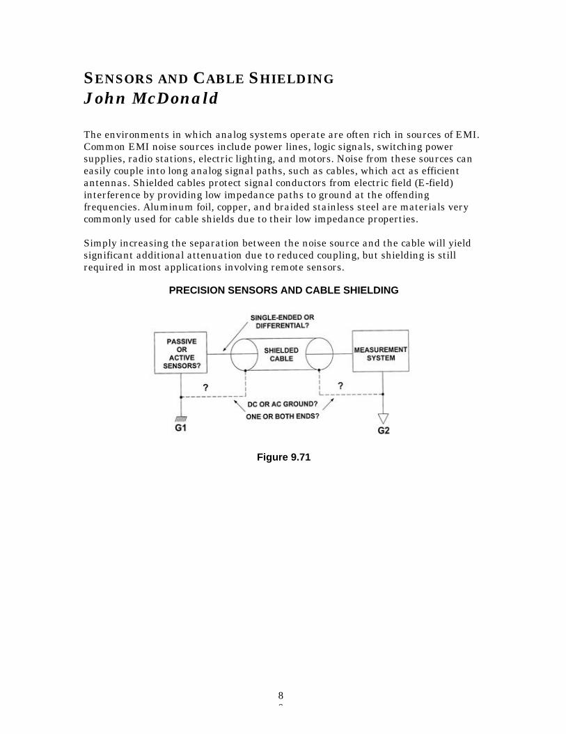
80
SENSORS AND CABLE SHIELDING
John McDonald
The environments in which analog systems operate are often rich in sources of EMI.Common EMI noise sources include power lines, logic signals, switching powersupplies, radio stations, electric lighting, and motors. Noise from these sources caneasily couple into long analog signal paths, such as cables, which act as efficientantennas. Shielded cables protect signal conductors from electric field (E-field)interference by providing low impedance paths to ground at the offendingfrequencies. Aluminum foil, copper, and braided stainless steel are materials verycommonly used for cable shields due to their low impedance properties.
Simply increasing the separation between the noise source and the cable will yieldsignificant additional attenuation due to reduced coupling, but shielding is stillrequired in most applications involving remote sensors.
PRECISION SENSORS AND CABLE SHIELDING
Figure 9.71
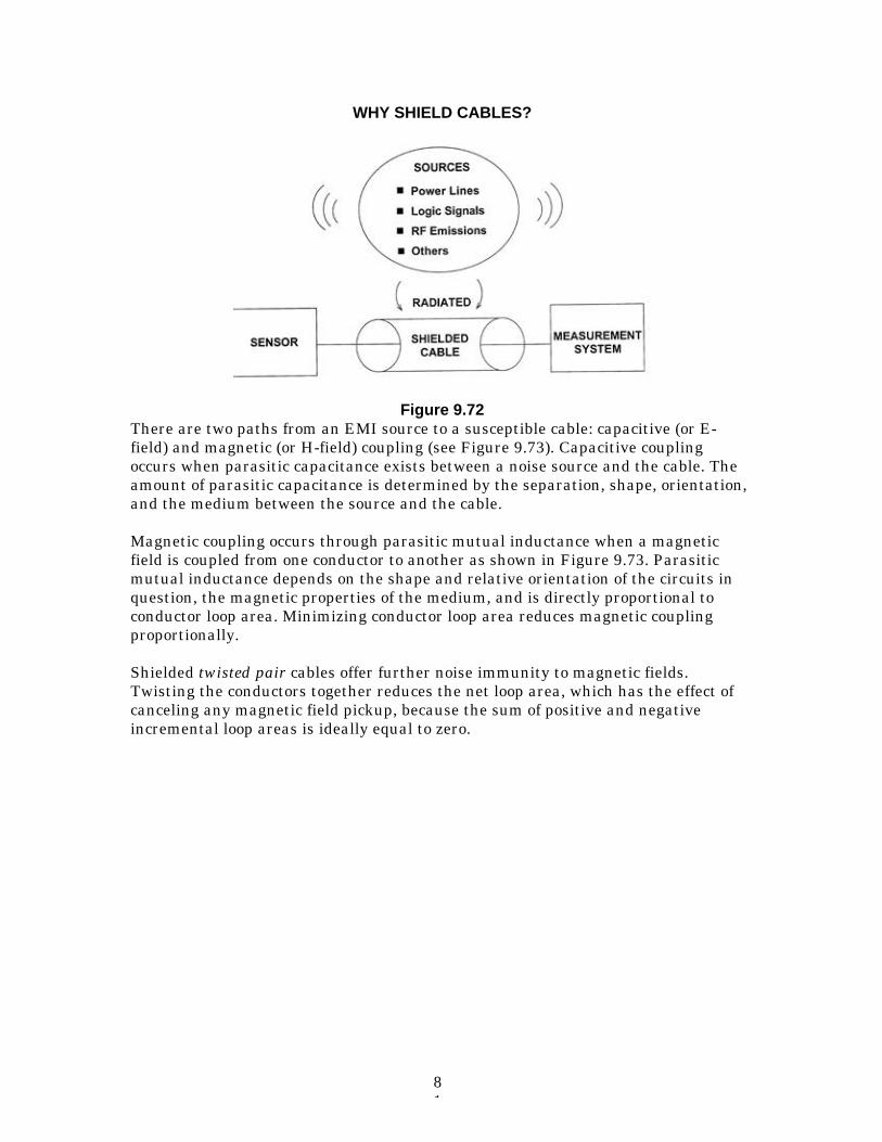
81
WHY SHIELD CABLES?
Figure 9.72There are two paths from an EMI source to a susceptible cable: capacitive (or E-field) and magnetic (or H-field) coupling (see Figure 9.73). Capacitive couplingoccurs when parasitic capacitance exists between a noise source and the cable. Theamount of parasitic capacitance is determined by the separation, shape, orientation,and the medium between the source and the cable.
Magnetic coupling occurs through parasitic mutual inductance when a magneticfield is coupled from one conductor to another as shown in Figure 9.73. Parasiticmutual inductance depends on the shape and relative orientation of the circuits inquestion, the magnetic properties of the medium, and is directly proportional toconductor loop area. Minimizing conductor loop area reduces magnetic couplingproportionally.
Shielded twisted pair cables offer further noise immunity to magnetic fields.Twisting the conductors together reduces the net loop area, which has the effect ofcanceling any magnetic field pickup, because the sum of positive and negativeincremental loop areas is ideally equal to zero.
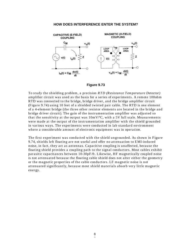
82
HOW DOES INTERFERENCE ENTER THE SYSTEM?
Figure 9.73
To study the shielding problem, a precision RTD (Resistance Temperature Detector)amplifier circuit was used as the basis for a series of experiments. A remote 100ohmRTD was connected to the bridge, bridge driver, and the bridge amplifier circuit(Figure 9.74) using 10 feet of a shielded twisted pair cable. The RTD is one elementof a 4-element bridge (the three other resistor elements are located in the bridge andbridge driver circuit). The gain of the instrumentation amplifier was adjusted sothat the sensitivity at the output was 10mV/°C, with a 5V full scale. Measurementswere made at the output of the instrumentation amplifier with the shield groundedin various ways. The experiments were conducted in lab standard environmentwhere a considerable amount of electronic equipment was in operation.
The first experiment was conducted with the shield ungrounded. As shown in Figure9.74, shields left floating are not useful and offer no attenuation to EMI-inducednoise, in fact, they act as antennas. Capacitive coupling is unaffected, because thefloating shield provides a coupling path to the signal conductors. Most cables exhibitparasitic capacitances between 10-30pF/ft. Likewise, HF magnetically coupled noiseis not attenuated because the floating cable shield does not alter either the geometryor the magnetic properties of the cable conductors. LF magnetic noise is notattenuated significantly, because most shield materials absorb very little magneticenergy.
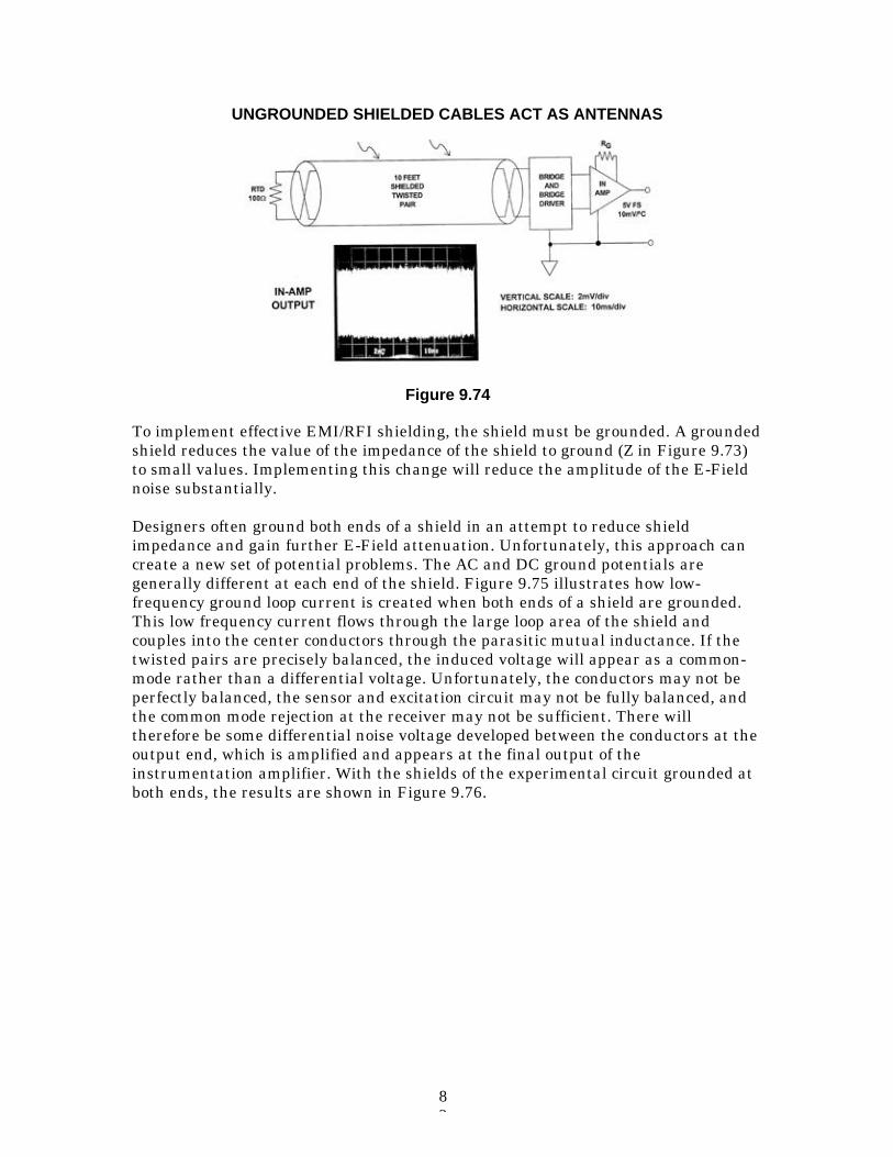
83
UNGROUNDED SHIELDED CABLES ACT AS ANTENNAS
Figure 9.74
To implement effective EMI/RFI shielding, the shield must be grounded. A groundedshield reduces the value of the impedance of the shield to ground (Z in Figure 9.73)to small values. Implementing this change will reduce the amplitude of the E-Fieldnoise substantially.
Designers often ground both ends of a shield in an attempt to reduce shieldimpedance and gain further E-Field attenuation. Unfortunately, this approach cancreate a new set of potential problems. The AC and DC ground potentials aregenerally different at each end of the shield. Figure 9.75 illustrates how low-frequency ground loop current is created when both ends of a shield are grounded.This low frequency current flows through the large loop area of the shield andcouples into the center conductors through the parasitic mutual inductance. If thetwisted pairs are precisely balanced, the induced voltage will appear as a common-mode rather than a differential voltage. Unfortunately, the conductors may not beperfectly balanced, the sensor and excitation circuit may not be fully balanced, andthe common mode rejection at the receiver may not be sufficient. There willtherefore be some differential noise voltage developed between the conductors at theoutput end, which is amplified and appears at the final output of theinstrumentation amplifier. With the shields of the experimental circuit grounded atboth ends, the results are shown in Figure 9.76.
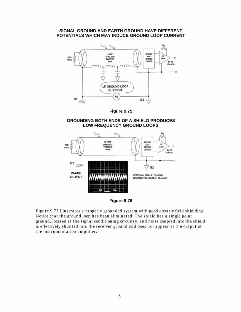
84
SIGNAL GROUND AND EARTH GROUND HAVE DIFFERENTPOTENTIALS WHICH MAY INDUCE GROUND LOOP CURRENT
Figure 9.75
GROUNDING BOTH ENDS OF A SHIELD PRODUCESLOW FREQUENCY GROUND LOOPS
Figure 9.76
Figure 9.77 illustrates a properly grounded system with good electric field shielding.Notice that the ground loop has been eliminated. The shield has a single pointground, located at the signal conditioning circuitry, and noise coupled into the shieldis effectively shunted into the receiver ground and does not appear at the output ofthe instrumentation amplifier.
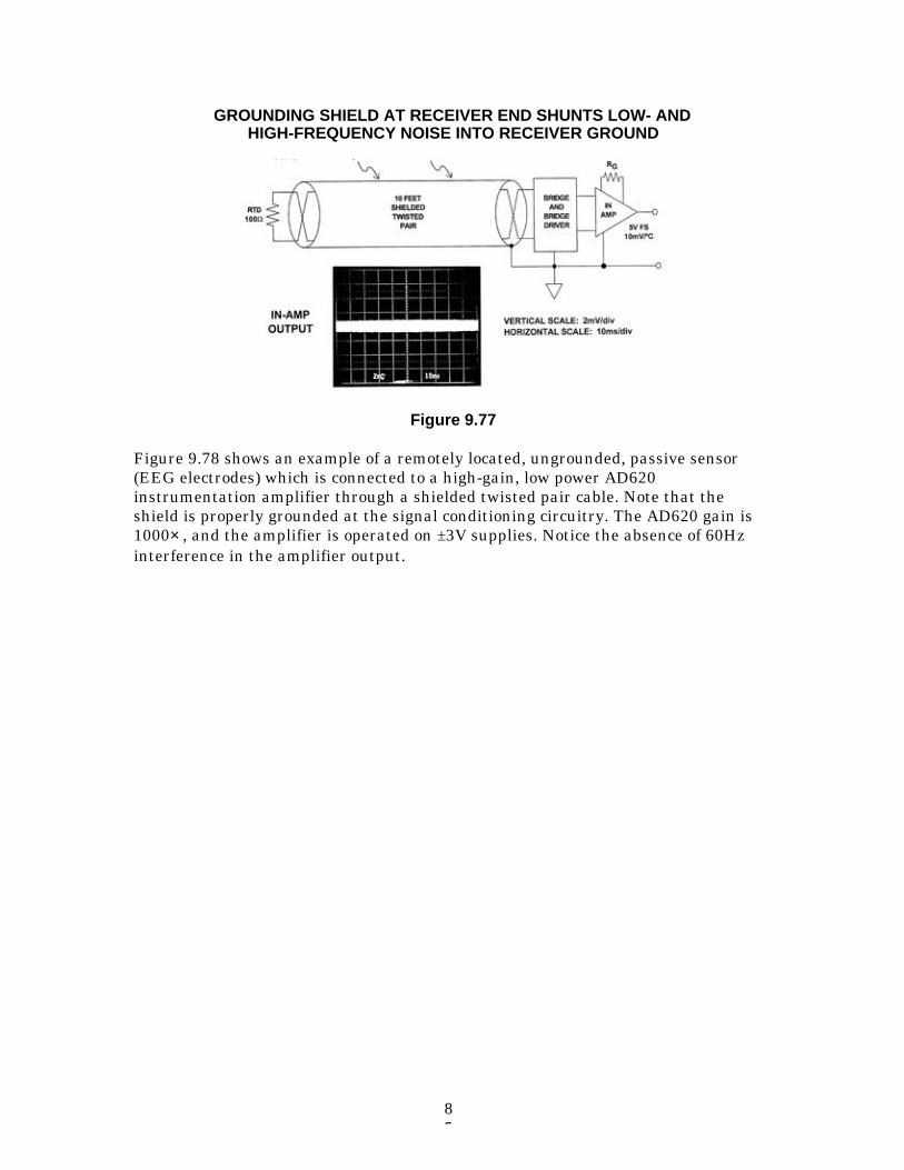
85
GROUNDING SHIELD AT RECEIVER END SHUNTS LOW- ANDHIGH-FREQUENCY NOISE INTO RECEIVER GROUND
Figure 9.77
Figure 9.78 shows an example of a remotely located, ungrounded, passive sensor(EEG electrodes) which is connected to a high-gain, low power AD620instrumentation amplifier through a shielded twisted pair cable. Note that theshield is properly grounded at the signal conditioning circuitry. The AD620 gain is1000× , and the amplifier is operated on ±3V supplies. Notice the absence of 60Hzinterference in the amplifier output.
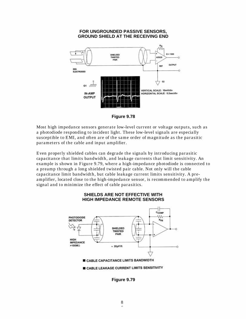
86
FOR UNGROUNDED PASSIVE SENSORS,GROUND SHIELD AT THE RECEIVING END
Figure 9.78
Most high impedance sensors generate low-level current or voltage outputs, such asa photodiode responding to incident light. These low-level signals are especiallysusceptible to EMI, and often are of the same order of magnitude as the parasiticparameters of the cable and input amplifier.
Even properly shielded cables can degrade the signals by introducing parasiticcapacitance that limits bandwidth, and leakage currents that limit sensitivity. Anexample is shown in Figure 9.79, where a high-impedance photodiode is connected toa preamp through a long shielded twisted pair cable. Not only will the cablecapacitance limit bandwidth, but cable leakage current limits sensitivity. A pre-amplifier, located close to the high-impedance sensor, is recommended to amplify thesignal and to minimize the effect of cable parasitics.
SHIELDS ARE NOT EFFECTIVE WITHHIGH IMPEDANCE REMOTE SENSORS
Figure 9.79
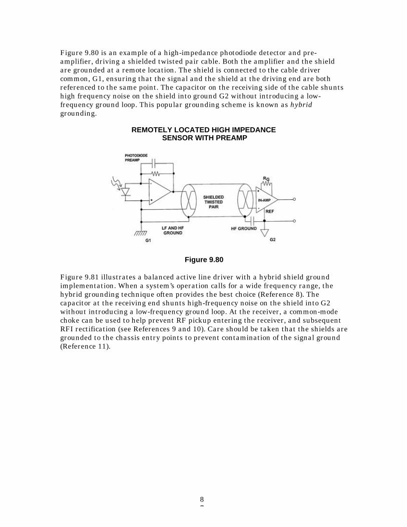
87
Figure 9.80 is an example of a high-impedance photodiode detector and pre-amplifier, driving a shielded twisted pair cable. Both the amplifier and the shieldare grounded at a remote location. The shield is connected to the cable drivercommon, G1, ensuring that the signal and the shield at the driving end are bothreferenced to the same point. The capacitor on the receiving side of the cable shuntshigh frequency noise on the shield into ground G2 without introducing a low-frequency ground loop. This popular grounding scheme is known as hybridgrounding.
REMOTELY LOCATED HIGH IMPEDANCE SENSOR WITH PREAMP
Figure 9.80
Figure 9.81 illustrates a balanced active line driver with a hybrid shield groundimplementation. When a system’s operation calls for a wide frequency range, thehybrid grounding technique often provides the best choice (Reference 8). Thecapacitor at the receiving end shunts high-frequency noise on the shield into G2without introducing a low-frequency ground loop. At the receiver, a common-modechoke can be used to help prevent RF pickup entering the receiver, and subsequentRFI rectification (see References 9 and 10). Care should be taken that the shields aregrounded to the chassis entry points to prevent contamination of the signal ground(Reference 11).
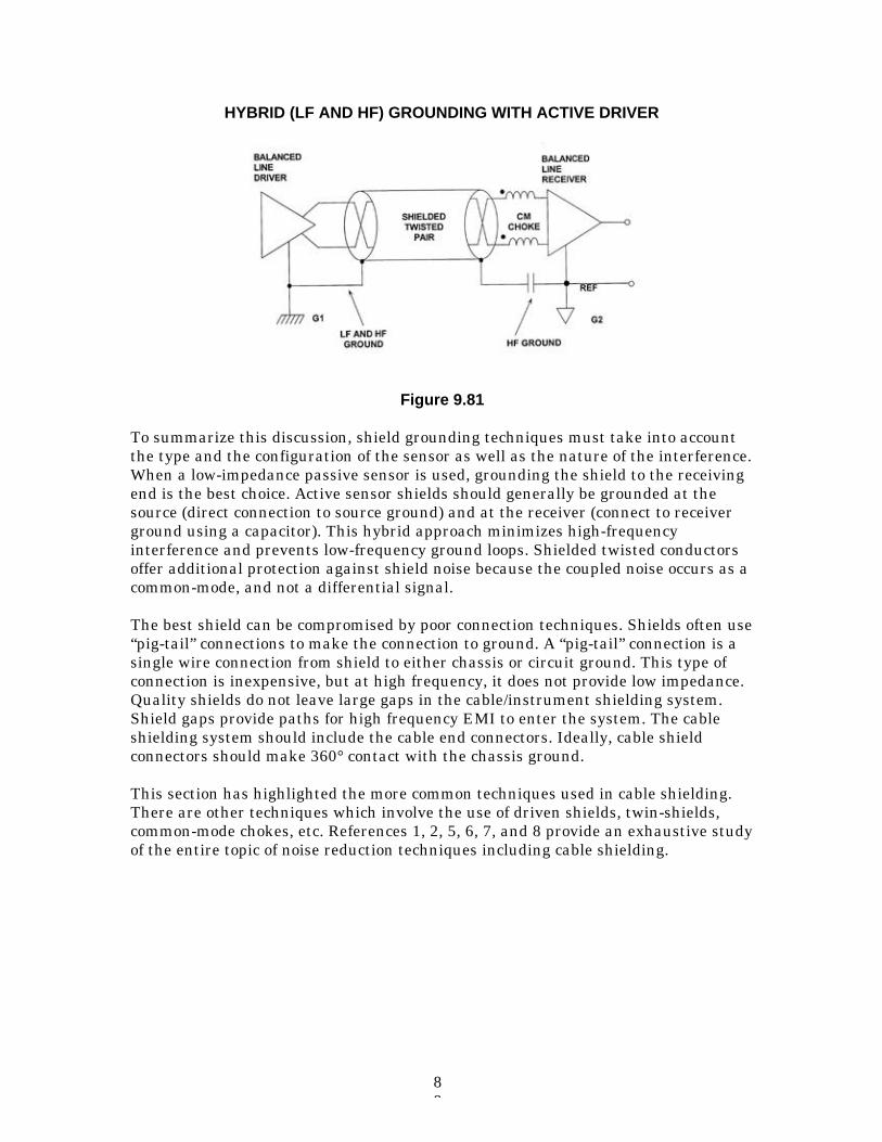
88
HYBRID (LF AND HF) GROUNDING WITH ACTIVE DRIVER
Figure 9.81
To summarize this discussion, shield grounding techniques must take into accountthe type and the configuration of the sensor as well as the nature of the interference.When a low-impedance passive sensor is used, grounding the shield to the receivingend is the best choice. Active sensor shields should generally be grounded at thesource (direct connection to source ground) and at the receiver (connect to receiverground using a capacitor). This hybrid approach minimizes high-frequencyinterference and prevents low-frequency ground loops. Shielded twisted conductorsoffer additional protection against shield noise because the coupled noise occurs as acommon-mode, and not a differential signal.
The best shield can be compromised by poor connection techniques. Shields often use“pig-tail” connections to make the connection to ground. A “pig-tail” connection is asingle wire connection from shield to either chassis or circuit ground. This type ofconnection is inexpensive, but at high frequency, it does not provide low impedance.Quality shields do not leave large gaps in the cable/instrument shielding system.Shield gaps provide paths for high frequency EMI to enter the system. The cableshielding system should include the cable end connectors. Ideally, cable shieldconnectors should make 360° contact with the chassis ground.
This section has highlighted the more common techniques used in cable shielding.There are other techniques which involve the use of driven shields, twin-shields,common-mode chokes, etc. References 1, 2, 5, 6, 7, and 8 provide an exhaustive studyof the entire topic of noise reduction techniques including cable shielding.
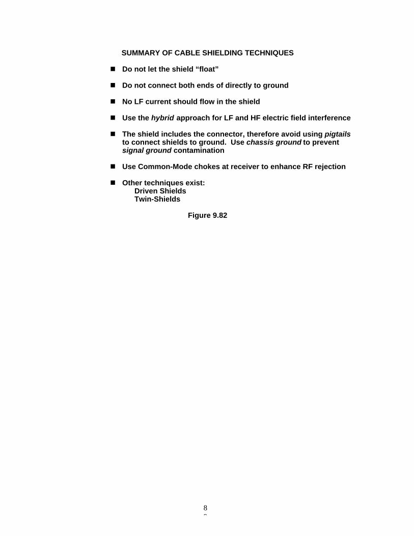
89
SUMMARY OF CABLE SHIELDING TECHNIQUES
Do not let the shield “float”
Do not connect both ends of directly to ground
No LF current should flow in the shield
Use the hybrid approach for LF and HF electric field interference
The shield includes the connector, therefore avoid using pigtailsto connect shields to ground. Use chassis ground to preventsignal ground contamination
Use Common-Mode chokes at receiver to enhance RF rejection
Other techniques exist:Driven ShieldsTwin-Shields
Figure 9.82
90
REFERENCES: SENSORS AND CABLE SHIELDING
1. H.W. Ott, Noise Reduction Techniques in Electronic Systems,Second Edition, John Wiley & Sons, Inc., New York, 1988.
2. Ralph Morrison, Grounding and Shielding Techniques inInstrumentation, Third Edition, John Wiley & Sons, Inc.,New York, 1988.
3. Systems Application Guide, Section 1, Analog Devices, Inc.,Norwood, MA, 1993.
4. AD620 Instrumentation Amplifier, Data Sheet, Analog Devices, Inc.
5. A. Rich, Understanding Interference-Type Noise, Analog Dialogue,16-3, 1982, pp. 16-19.
6. A. Rich, Shielding and Guarding, Analog Dialogue, 17-1, 1983,pp. 8-13.
7. EDN’s Designer’s Guide to Electromagnetic Compatibility, EDN,January, 20, 1994, material reprinted by permission of CahnersPublishing Company, 1995.
8. Designing for EMC (Workshop Notes), Kimmel Gerke Associates,Ltd., 1994.
9. James Bryant and Herman Gelbach, High Frequency SignalContamination, Analog Dialogue, Vol. 27-2, 1993.
10. Walt Jung, System RF Interference Prevention, Analog Dialogue,Vol. 28-2, 1994.
11. Neil Muncy, Noise Susceptibility in Analog and Digital SignalProcessing Systems, presented at 97th Audio Engineering SocietyConvention, Nov. 1994.
91
GENERAL REFERENCES: HARDWAREDESIGN TECHNIQUES
1. Linear Design Seminar, Section 11, Analog Devices, Inc., 1995.
2. E.S.D. Prevention Manual Available free from Analog Devices, Inc.
3. B.I. & B. Bleaney, Electricity & Magnetism, OUP 1957, pp 23,24, & 52.
4. Paul Brokaw, An I.C. Amplifier User's Guide to Decoupling, Groundingand Making Things Go Right for a Change, Analog Devices Application Note, Available free of charge from Analog Devices, Inc.
5. Jeff Barrow, Avoiding Ground Problems in High Speed Circuits,R.F. Design, July 1989.
AND
Paul Brokaw & Jeff Barrow, Grounding for Low- and High-FrequencyCircuits, Analog Dialogue, 23-3 1989.
Free from Analog Devices.
6. International EMI Emission Regulations Canada CSA C108.8-M1983 FDR VDE 0871/VDE 0875 Japan CISPR (VCCI)/PUB 22 USA FCC-15 Part J
7. Bill Slattery & John Wynne, Design & Layout of a Video Graphics Systemfor Reduced EMI, Analog Devices Application Note (E1309-15-10/89)
Free from Analog Devices.
8. William R. Blood, Jr., MECL System Design Handbook(HB205, Rev. 1), Motorola Semiconductor Products, Inc., 1988.
9. Wainwright Instruments Inc., 7770 Regents Rd., #113, Suite 371,San Diego, CA 92122, Tel. 619-558-1057, Fax. 619-558-1019.
Wainwright Instruments GmbH, Widdersberger Strasse 14,DW-8138 Andechs-Frieding, Germany. Tel: +49-8152-3162,Fax: +49-8152-40525.
10. Ralph Morrison, Grounding and Shielding Techniques inInstrumentation, Third Edition, John Wiley, Inc., 1986.
11. Henry W. Ott, Noise Reduction Techniques in Electronic Systems,Second Edition, John Wiley, Inc., 1988.
92
12. Robert A. Pease, Troubleshooting Analog Circuits, Butterworth-Heinemann, 1991.
13. Jim Williams, Editor, Analog Circuit Design: Art, Science, andPersonalities, Butterworth-Heinemann, 1991.
14. Doug Grant and Scott Wurcer, Avoiding Passive Component Pitfalls,The Best of Analog Dialogue, pp. 143-148, Analog Devices, Inc., 1991.
15. Walt Jung and Richard Marsh, Picking Capacitors, Part I., Audio,February, 1980.
16. Walt Jung and Richard Marsh, Picking Capacitors, Part II., Audio,March, 1980.
17. Daryl Gerke and Bill Kimmel, The Designer's Guide to Electromagnetic Compatibility, EDN Supplement, January 20, 1994.
18. Walt Kester, Basic Characteristics Distinguish Sampling A/D Converters,EDN, September 3, 1992, pp.135-144.
19. Walt Kester, Peripheral Circuits Can Make or Break Sampling ADCSystem, EDN, October 1, 1992, pp. 97-105.
20. Walt Kester, Layout, Grounding, and Filtering Complete SamplingADC System, EDN, October 15, 1992, pp. 127-134.