SECTION 5: THESIS DETAILS NUMBER OF PAGES DEDICATION
137
Thesis Template Converter Form - Section 7 / Arash Badami Behjat Signature __________ SECTION 5: THESIS DETAILS NUMBER OF PAGES Page number on the last page of this document: 103 DEDICATION Dedication [Max 2 lines] ACKNOWLEDGMENTS* I would like to thank TUBITAK for funding this work. I would like to thanks Prof. Ahmet Oral for all his supports during my master's study and providing me a great chance to get trained, work and collaborate in the NanoMagnetics Instrument company. These three years were an opportunity to get in touch with expert people who help me to overcome problems as well as doing experiments with various microscopes. I would like to thank Prof. Tofik Mamadov who helped me a lot in instruments installation. I thank Muherram Demir, Hilal Gozler, Kazim Ayhan, Seda Surucu and all NanoMagnetics Instruments family for all their efforts and help to finish this project. I would like to thank my lab mates and my friends Shayeste Moravati, Parisa Sharif, and Muammer Kozan, who helped me in my tough times. And finally I do appreciate my family, specially my mother who always pushes me forward in all my level of my life. * If you have received project support from TÜBİTAK, you must mention about it.
Transcript of SECTION 5: THESIS DETAILS NUMBER OF PAGES DEDICATION

Thesis Template Converter Form - Section 7 / Arash Badami Behjat Signature __________
SECTION 5: THESIS DETAILS
NUMBER OF PAGES
Page number on the last page of this document: 103
DEDICATION
Dedication [Max 2 lines]
ACKNOWLEDGMENTS*
I would like to thank TUBITAK for funding this work.
I would like to thanks Prof. Ahmet Oral for all his supports during my master's study and providing me
a great chance to get trained, work and collaborate in the NanoMagnetics Instrument company. These
three years were an opportunity to get in touch with expert people who help me to overcome problems
as well as doing experiments with various microscopes.
I would like to thank Prof. Tofik Mamadov who helped me a lot in instruments installation.
I thank Muherram Demir, Hilal Gozler, Kazim Ayhan, Seda Surucu and all NanoMagnetics Instruments
family for all their efforts and help to finish this project.
I would like to thank my lab mates and my friends Shayeste Moravati, Parisa Sharif, and Muammer
Kozan, who helped me in my tough times.
And finally I do appreciate my family, specially my mother who always pushes me forward in all my
level of my life.
* If you have received project support from TÜBİTAK, you must mention about it.

ULTRA-HIGH-RESOLUTION LOW-TEMPERATURE MAGNETIC FORCE
MICROSCOPY
A THESIS SUBMITTED TO
THE GRADUATE SCHOOL OF NATURAL AND APPLIED SCIENCES
OF
MIDDLE EAST TECHNICAL UNIVERSITY
BY
ARASH BADAMI BEHJAT
IN PARTIAL FULFILLMENT OF THE REQUIREMENTS
FOR
THE DEGREE OF MASTER OF SCIENCE
IN
PHYSICS
SEPTEMBER 2019


Approval of the thesis:
ULTRA-HIGH-RESOLUTION LOW-TEMPERATURE MAGNETIC FORCE
MICROSCOPY
submitted by ARASH BADAMI BEHJAT in partial fulfillment of the requirements
for the degree of Master of Science in Physics Department, Middle East Technical
University by,
Prof. Dr. Halil Kalıpçılar
Dean, Graduate School of Natural and Applied Sciences
Prof. Dr. Altug Ozpineci
Head of Department, Physics
Prof. Dr. Ahmet Oral
Supervisor, Physics, METU
Examining Committee Members:
Assoc. Prof. Dr. Sinan Kaan Yerli
Physics, METU
Prof. Dr. Ahmet Oral
Physics, METU
Assoc. Prof. Dr. Şinasi Barış Emre
Engineering Physics, Ankara University
Date: 09.09.2019

iv
I hereby declare that all information in this document has been obtained and
presented in accordance with academic rules and ethical conduct. I also declare
that, as required by these rules and conduct, I have fully cited and referenced all
material and results that are not original to this work.
Name, Surname:
Signature:
Arash Badami Behjat

v
ABSTRACT
ULTRA-HIGH-RESOLUTION LOW-TEMPERATURE MAGNETIC FORCE
MICROSCOPY
Badami Behjat, Arash
Master of Science, Physics
Supervisor: Prof. Dr. Ahmet Oral
September 2019, 103 pages
Scanning probe microscopy is a conventional technic which has opened new methods
to investigate surface properties. Imaging atoms or manipulating them as well as
measuring surface structures with high resolution and accuracy are fantastic features
which are utilized in surface science to study the characterization of materials. Atomic
Force Microscopy (AFM) a standard popular method can measure the interaction
forces between the sharp tip and the sample surface. This method allows us imaging
atoms individually with the atomic resolution or the structure of molecules. AFM
could measure various types of forces like van der Waals, electrostatic, friction or
magnetic forces under the different environment condition, high vacuum or Ultra high
vacuum, ambient, and aqua, as well as high magnetic field at room or cryogenic
temperature. Affordable price, easy sample preparation, and operation, specifically
high resolution down to the nanometer are the advantages of this method. Moreover,
ability to image almost any type of samples such surface of the ceramic material, or
the dispersion of the metallic nanoparticles, or so soft material, such very flexible
polymers, the human cell, and DNA is the most considerable advantages of AFM.
Magnetic Force Microscopy (MFM) is another standard method for surface
investigation of magnetic properties, which is the aim of this thesis. MFM is one of
the significant roles in material science that magnetic resolution of 10 nm and less,

vi
provides critical information in the different area of science such as spintronics, spin
glass system, magnetic nanoparticles, superconductivity, high-density magnetic
recording media, magnetic phase transition, etc. The capability of AFM/MFM in
working at a low-temperature range of 300 kelvin to hundreds of millikelvin increases
the versatility of the microscope.
Principally, low-temperature Atomic/Magnetic Force Microscope (LT-AFM/MFM)
is working with the measuring the cantilever deflection; This means the fiber
interferometer which directs the laser light to the cantilever tip by a fiber cable can
measure the deflection with calculating the percentage of laser light coming back from
the tip. The significant role here is the operation of the microscope in extremely low
temperature for further material evaluation and also the reliability of working that in
various temperature properly.
The critical issue is microscope alignment, which the cantilever and fiber respectively
could collapse in the cooling status. Therefore, the design of the microscope head
should be wholly centric, and a particular mechanism aligns considering the different
thermal contraction of the material. Besides, most cryogenic systems are limited in the
sample space; consequently, this limitation should be applied in the whole design and
system alignment.
In my master thesis, I have improved a Low-Temperature Fabry-Perot Atomic Force
Microscope / Magnetic Force Microscope (LT-AFM/MFM). This instrument was
developed earlier in our group and used standard tips and a Fabry-Perot fiber
interferometer for measuring the cantilever deflection. The earlier version of this LT-
AFM had some reliability issues with the fiber nanopositioner at low temperatures.
Principally, in a Fabry-Perot AFM/MFM it is required to reduce the distance between
cantilever and fiber by moving the latter. This issue is also an essential means to
improve the resolution because thereby, the signal intensity of the reflected light can
be increased. In the previous setup, the piezo nanopositioner was not able to move the
ferrule that holds to fiber, due to the limited space in the vertical direction in the
vii
cryostat. Therefore, I modified the design, resulting in improved reliability of the fiber
nanopositioner. This was achieved by (1) centering the AFM tip at the piezo tube; (2)
improving the surface quality of the groves in which the ferrule is sliding; (3)
increasing the inertial mass of the fiber holder.
The new concentric design enabled the piezoelectric nanopositioner not only to move
the fiber forward and backward in the vertical direction but also worked reliably and
precisely at extremely low temperatures down to 300 milliKelvins. The movability of
the fiber to optimize its position with respect to the cantilever is essential for the
performance of the microscope. Thereby the slope is increased, i.e., the change of the
signal at the photodiode with respect to a change of cantilever position, of the reflected
laser signal, and hence the vertical resolution of the AFM. With this new design, a
slope of 148 (mV/Ȧ) was reached using a laser power of 3.5 mW, whereas before the
slope only amounted to 120 (mV/Ȧ). Increasing this slope also means improved
vertical resolution in AFM and MFM as well.
In this research, we have improved the previously developed AFM/MFM Fabry-Perot
low-temperature microscope with an outer dimension less than 25.4 mm which is
completely commercialized for various types of cryogen-free cryostats from different
manufacturers or liquid He bathes. All measurements conducted in the newly installed
cryogen-free cryostat with the capability to reach 1.3 K from Cryomagnetic
instrument; This ultra-low temperature is a vital issue in material science and also
physics investigation on many phenomenon. The working potential of the
microscope, in both AFM and MFM mode at various temperature, besides ultra-low
noise level around 25 fm/Hz1/2 in 300 K and 12 fm/Hz1/2 in 1 K gives high-resolution
images.

viii
Keywords: Atomic force microscope, AFM, magnetic force microscope, MFM, low
temperature, magnetic field, high resolution imaging, cryostat, milliKelvin, fibre
interferometer, fibre Fabry-Pérot interferometer
ix
ÖZ
ULTRA-YÜKSEK-ÇÖZÜNÜRLÜK DÜŞÜK SICAKLIKLI MANYETİK
KUVVET MİKROSKOPİSİ
Badami Behjat, Arash
Yüksek Lisans, Fizik
Tez Danışmanı: Prof. Dr. Ahmet Oral
Eylül 2019, 103 sayfa
Tarama probu mikroskobu, yüzey özelliklerini araştırmak için yeni yöntemler açan
geleneksel bir tekniktir. Atomları görüntülemek veya bunları manipüle etmek, aynı
zamanda yüzey yapılarını yüksek çözünürlük ve hassasiyetle ölçmek, malzemelerin
karakterizasyonunu incelemek için yüzey biliminde kullanılan fantastik özelliklerdir.
Atomik Kuvvet Mikroskobu (AFM) standart bir popüler yöntemdir, keskin uç ile
numune yüzeyi arasındaki etkileşim kuvvetlerini ölçebilir. Bu yöntem atomları atomik
çözünürlük veya moleküllerin yapısı ile ayrı ayrı görüntülememize izin verir. AFM,
farklı ortam koşulları altında van der Waals, elektrostatik, sürtünme veya manyetik
kuvvetler, yüksek vakum veya Ultra yüksek vakum, ortam ve su ve ayrıca oda veya
kriyojenik sıcaklıktaki yüksek manyetik alan gibi çeşitli kuvvetleri ölçebilir. Uygun
fiyat, kolay numune hazırlama ve işletme, özellikle nanometreye kadar yüksek
çözünürlük bu yöntemin avantajlarıdır. . Ayrıca, seramik malzemenin yüzeyi veya
metalik nano partiküllerin ya da çok yumuşak polimerlerin, çok esnek polimerlerin,
insan hücresinin ve DNA'nın dağılması gibi hemen hemen her tür numuneyi
görüntüleyebilme yeteneği, AFM'nin en önemli avantajlarıdır.
Manyetik Kuvvet Mikroskobu (MFM), bu tezin amacı olan manyetik özelliklerin
yüzey araştırması için başka bir standart yöntemdir. MFM, 10 nm ve daha düşük
manyetik çözünürlüğe sahip malzeme bilimi alanındaki önemli rollerden biridir;
x
spintronics, spin cam sistemi, manyetik nanopartiküller, süper iletkenlik, yüksek
yoğunluklu manyetik kayıt ortamı, manyetik faz gibi farklı bilim alanlarında kritik
bilgiler sağlar. geçiş, vb. AFM / MFM'nin 300 kelvin ila yüzlerce millikelvin düşük
sıcaklık aralığında çalışma kabiliyeti mikroskobun çok yönlülüğünü arttırır.
Prensip olarak, düşük sıcaklıkta Atomik / Manyetik Kuvvet Mikroskobu (LT-AFM /
MFM), konsol sapmalarının ölçülmesi ile çalışmaktadır; Bu, lazer ışığını bir fiber
kablo ile konsol ucuna yönlendiren fiber interferometresinin, sapmadan geri dönen
lazer ışığının yüzdesini hesaplayarak sapmayı ölçebileceği anlamına gelir. Buradaki
önemli rol, mikroskobun daha fazla malzeme değerlendirmesi için son derece düşük
sıcaklıklarda çalışması ve aynı zamanda çeşitli sıcaklıklarda uygun şekilde çalışmanın
güvenilirliğidir.
Kritik sorun, konsol ve elyafın sırasıyla soğutma durumunda çökebileceği mikroskop
dizilimidir. Bu nedenle, mikroskop kafasının tasarımı tamamen merkezli olmalı ve
malzemenin farklı termal büzülmesini göz önünde bulundurarak belirli bir mekanizma
aynı hizada olmalıdır. Ayrıca, çoğu kriyojenik sistem numune alanında sınırlıdır;
sonuç olarak, bu sınırlama tüm tasarım ve sistem uyumunda uygulanmalıdır.
Yüksek lisans tezimde Düşük Sıcaklıkta Fabry-Perot Atomik Kuvvet Mikroskobu /
Manyetik Kuvvet Mikroskobu (LT-AFM / MFM) geliştirdim. Bu cihaz grubumuzda
daha önce geliştirildi ve konsol sapmasını ölçmek için standart uçlar ve bir Fabry-
Perot fiber interferometre kullanıldı. Bu LT-AFM'nin önceki versiyonunda düşük
sıcaklıklarda fiber nanopozlayıcı ile bazı güvenilirlik sorunları vardı. Prensip olarak,
bir Fabry-Perot AFM / MFM'de, ikincisini hareket ettirerek konsol ile fiber arasındaki
mesafeyi azaltmak gerekir. Bu sorun aynı zamanda çözünürlüğü iyileştirmek için
gerekli bir araçtır, çünkü yansıyan ışığın sinyal yoğunluğu artabilir. Önceki
kurulumda, piezo nanopozlayıcı, kriyostattaki düşey doğrultuda sınırlı alan nedeniyle
elyafı tutan yüksüğü hareket ettiremedi. Bu nedenle, tasarımı değiştirdim, böylece
elyaf nanopozitörünün güvenilirliğini arttırdım. Bu, (1) piez tüpünde AFM ucunun
xi
merkezlenmesi; (2) yüksük kaydığı yivlerin yüzey kalitesini iyileştirmek; (3) elyaf
tutucunun atalet kütlesinin arttırılması.
Yeni eşmerkezli tasarım, piezoelektrik nanopozitifin sadece fiberi dikey yönde ileri
ve geri hareket ettirmekle kalmayıp, aynı zamanda 300 miliKelvin'e kadar olan aşırı
düşük sıcaklıklarda da güvenilir ve hassas bir şekilde çalıştı. Elyafın konsoluna göre
konumunu optimize etme hareketi mikroskobun performansı için önemlidir. Böylece
eğim, yani, fotodiyottaki sinyalin, konsol pozisyonunun, yansıyan lazer sinyalinin
değişmesine ve dolayısıyla AFM'nin dikey çözünürlüğüne bağlı olarak değişmesi ile
artar. Bu yeni tasarımla, 3.5 mW'lık bir lazer gücü kullanılarak 148 (mV / Ȧ) eğime
ulaşılırken, eğimden önce sadece 120 (mV / Ȧ) değerindeydi. Bu eğimi arttırmak,
AFM ve MFM'de de dikey çözünürlüğün artması demektir.
Bu araştırmada, daha önce geliştirilen AFM / MFM Fabry-Perot düşük sıcaklık
mikroskobunu, 25,4 mm'den daha düşük bir dış boyutu olan, farklı üreticilerden veya
sıvı He banyolarından gelen çeşitli kriyojen içermeyen kriyolar için tamamen
ticarileştirilmiş şekilde geliştirdik. Yeni kurulan kriyojensiz kriyostatta yapılan ve tüm
ölçümler Kriyognetik cihazdan 1,3 K değerine ulaşabilir; Bu ultra düşük sıcaklık,
malzeme biliminde hayati bir konudur ve aynı zamanda birçok fenomen üzerinde fizik
araştırması yapar. Mikroskopun hem AFM hem de MFM modunda çeşitli
sıcaklıklarda çalışma potansiyeli, 300 K'da 25 fm / Hz1 / 2 ve 1 K'da 12 fm / Hz1 / 2
civarında ultra düşük gürültü seviyesi yüksek çözünürlüklü görüntüler verir.
Anahtar Kelimeler: Atomik kuvvet mikroskobu, AFM, manyetik kuvvet mikroskobu,
MFM, düşük sıcaklık, manyetik alan, yüksek çözünürlüklü görüntüleme, kriyostat,
milliKelvin, fiber interferometre, fiber Fabry-Pérot interferometre

xii
ACKNOWLEDGEMENTS
I would like to thank TUBITAK for funding this work.
I would like to thanks Prof. Ahmet Oral for all his supports during my master's study
and providing me a great chance to get trained, work and collaborate in the
NanoMagnetics Instrument company. These three years were an opportunity to get in
touch with expert people who help me to overcome problems as well as doing
experiments with various microscopes.
I would like to thank Prof. Tofik Mamadov who helped me a lot in instruments
installation.
I thank Muherram Demir, Hilal Gozler, Kazim Ayhan, Seda Surucu and all
NanoMagnetics Instruments family for all their efforts and help to finish this project.
I would like to thank my lab mates and my friends Shayeste Moravati, Parisa Sharif,
and Muammer Kozan, who helped me in my tough times.
And finally I do appreciate my family, specially my mother who always pushes me
forward in all my level of my life.
xiii
TABLE OF CONTENTS
ABSTRACT ................................................................................................................. v
ÖZ ............................................................................................................................ ix
ACKNOWLEDGEMENTS ...................................................................................... xii
TABLE OF CONTENTS ......................................................................................... xiii
LIST OF TABLES .................................................................................................. xvii
LIST OF FIGURES ............................................................................................... xviii
LIST OF ABBREVIATIONS ................................................................................ xxiv
LIST OF SYMBOLS ............................................................................................. xxvi
CHAPTERS
1. INTRODUCTION ................................................................................................ 1
1.1. Introduction and Overview ................................................................................ 1
1.2. Work Plan .......................................................................................................... 5
2. MAGNETIC FORCE MICROSCOPY ................................................................ 7
2.1. Magnetic Force Microscopy (MFM) ................................................................. 7
2.1.1. Applicability ............................................................................................. 10
2.2. Operation Theory ............................................................................................ 10
2.2.1. Dynamic Mode ......................................................................................... 10
2.2.2. Static Mode ............................................................................................... 14
2.2.3. Tip-Sample Magnetic Interaction ............................................................. 15
2.2.4. Lennard-Jones Potential ............................................................................ 15
xiv
3. Mıcroscope Instrumentatıon .............................................................................. 19
3.1. Microscope Instrumentation ........................................................................... 19
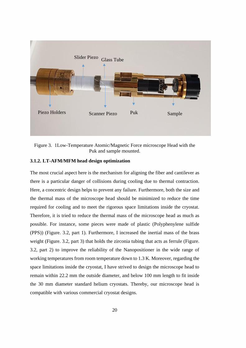
3.1.1. Low-Temperature AFM/MFM Head ....................................................... 19
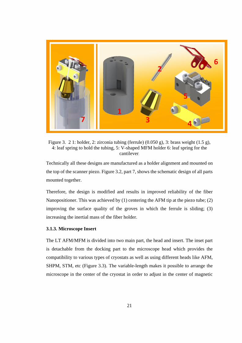
3.1.2. LT-AFM/MFM head design optimization ............................................... 20
3.1.3. Microscope Insert ..................................................................................... 21
3.1.4. Operation mechanism ............................................................................... 22
3.1.5. Approach and Retract Mechanism ........................................................... 27
3.1.6. Sample Positioning in the X-Y direction ................................................. 28
3.1.7. Fine Approach Mechanism ...................................................................... 30
3.2. MFM Alignment Holder ................................................................................. 30
3.2.1. Alignment Holder Design ........................................................................ 30
3.2.2. Fiber Cable ............................................................................................... 33
3.2.3. Cantilevers ................................................................................................ 33
3.3. Optical laser Interferometer method ............................................................... 34
3.3.1. Michelson Fiber Interferometer Principal and design .............................. 35
3.3.2. LT-AFM controller ................................................................................... 36
4. Low-Temperature ExperIments ........................................................................ 39
4.1. Low-Temperature alignment mechanism Tests .............................................. 39
4.2. Noise Analysis ................................................................................................ 42
4.2.1. Laser Noise ............................................................................................... 42
4.2.2. Shot Noise ................................................................................................ 43
4.2.3. Electrical Noise ........................................................................................ 44
4.2.4. Johnson Noise ........................................................................................... 44
4.2.5. Current and Voltage noise ........................................................................ 44

xv
4.2.6. Total Noise ................................................................................................ 44
4.2.7. Noise measurements ................................................................................. 44
4.3. Images ............................................................................................................. 46
4.3.1. Tapping Mode AFM Image ...................................................................... 46
4.3.2. MFM Images............................................................................................. 50
4.3.3. Magnetic Poles .......................................................................................... 50
4.3.4. Lift-Height Adjustment............................................................................. 50
4.3.5. The MFM tip Size ..................................................................................... 52
5. Low temperature ................................................................................................ 55
5.1. The Cryogenic temperature ............................................................................. 55
5.2. Introduction to LT-AFM/MFM ....................................................................... 56
5.2.1. Dry Cryostat .............................................................................................. 57
5.3. Cryocoolers ..................................................................................................... 58
5.4. Vibration Isolation ........................................................................................... 64
5.4.1. Vibration Isolation Performance:.............................................................. 66
5.5. Images ............................................................................................................. 68
5.6. Conclusion ....................................................................................................... 70
6. Fabry Perot Interferometer.................................................................................. 71
6.1. Introduction ..................................................................................................... 71
6.2. Fiber Coating ................................................................................................... 72
6.2.1. Fiber coating with TiO2 ............................................................................ 73
6.3. Fiber Slider ...................................................................................................... 73
6.3.1. Fiber Slider Design for Low Temperature ................................................ 73
6.3.2. Drive Mechanism of the Fiber Slider ....................................................... 75
xvi
6.3.3. Testing the Slip-Stick Mechanism at Low Temperature .......................... 76
6.3.4. Slope and Visibility Behavior vs gap distance between the Cantilever and
Fiber .................................................................................................................... 78
6.3.5. Fiber Optic Circulator .............................................................................. 79
6.4. Fiber Fabry-Perot interferometer .................................................................... 80
6.5. Experimental Results ...................................................................................... 83
6.5.1. Fabry-Perot Interferometer signal ............................................................ 83
6.5.2. AFM Images: ............................................................................................ 85
6.5.3. MFM Images ............................................................................................ 88
6.5.4. Conclusions .............................................................................................. 92
7. conclusion ........................................................................................................... 93
REFERENCES .......................................................................................................... 95
xvii
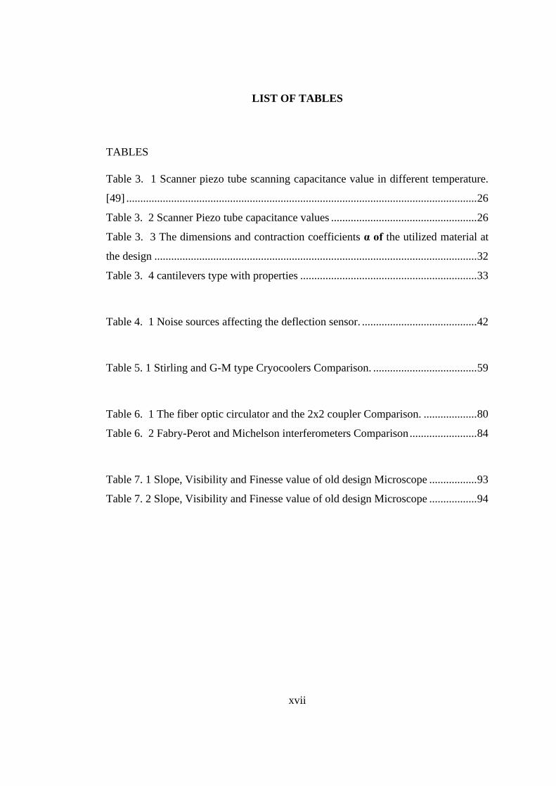
LIST OF TABLES
TABLES
Table 3. 1 Scanner piezo tube scanning capacitance value in different temperature.
[49] ............................................................................................................................. 26
Table 3. 2 Scanner Piezo tube capacitance values .................................................... 26
Table 3. 3 The dimensions and contraction coefficients α of the utilized material at
the design ................................................................................................................... 32
Table 3. 4 cantilevers type with properties ............................................................... 33
Table 4. 1 Noise sources affecting the deflection sensor. ......................................... 42
Table 5. 1 Stirling and G-M type Cryocoolers Comparison. ..................................... 59
Table 6. 1 The fiber optic circulator and the 2x2 coupler Comparison. ................... 80
Table 6. 2 Fabry-Perot and Michelson interferometers Comparison ........................ 84
Table 7. 1 Slope, Visibility and Finesse value of old design Microscope ................. 93
Table 7. 2 Slope, Visibility and Finesse value of old design Microscope ................. 94

xviii
LIST OF FIGURES
FIGURES
Figure 1. 1Earliest design of the AFM with an optical lever in the 1920s. [6] ........... 2
Figure 1. 2 schematic of scanning tunneling microscopy. [12] ................................... 3
Figure 1. 3 STM image, (a) Topography, (b) Size of the Graphite on the HOPG. ..... 4
Figure 1. 4 AFM image of the 200 nm Nickle Oxide coated on the glass .................. 5
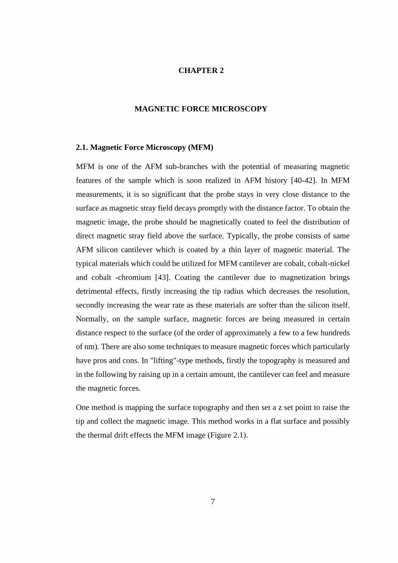
Figure 2. 1 lifting the tip of the surface. [6] ................................................................. 8
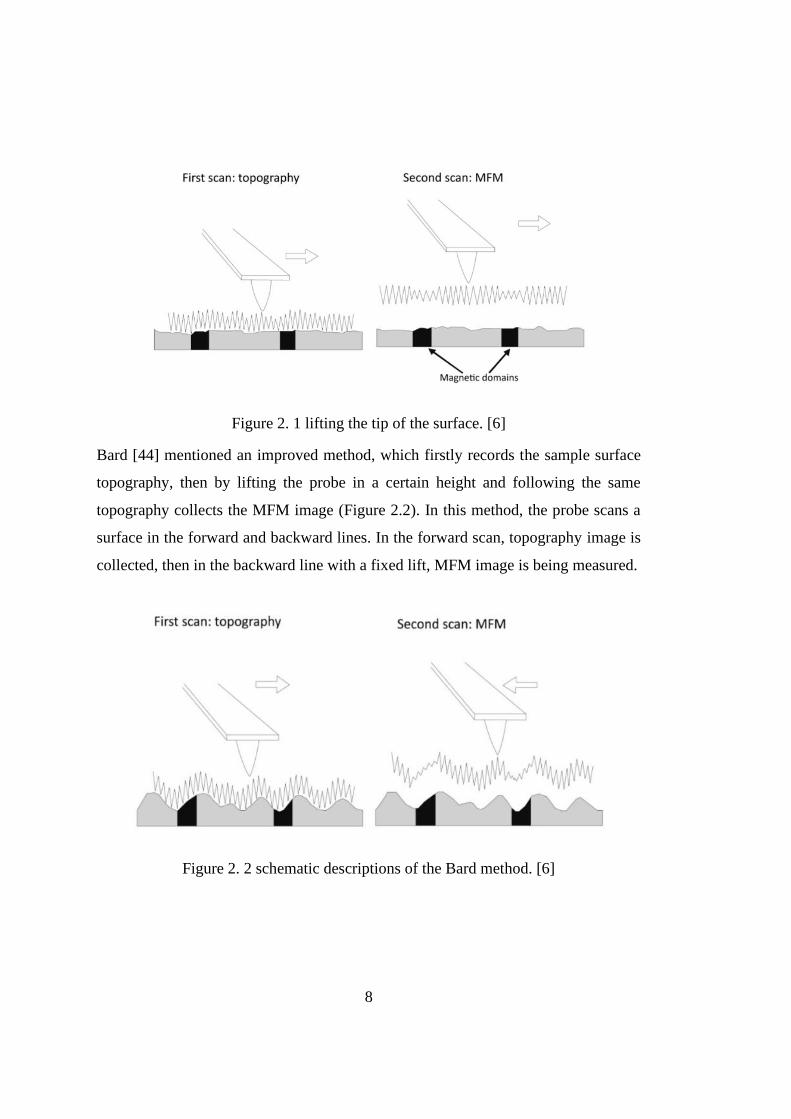
Figure 2. 2 schematic descriptions of the Bard method. [6] ........................................ 8
Figure 2. 3 z set-point oscillation. [6] .......................................................................... 9
Figure 2. 4Schematic descriptions of the Hosaka method. [6] .................................... 9
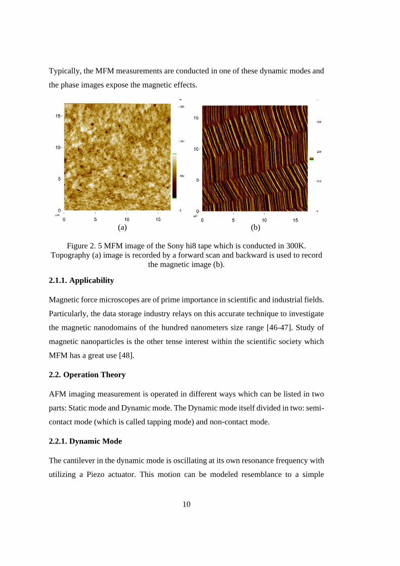
Figure 2. 5 MFM image of the Sony hi8 tape which is conducted in 300K. Topography
(a) image is recorded by a forward scan and backward is used to record the magnetic
image (b). ................................................................................................................... 10
Figure 2. 6 The schematic resemblance of a spring-mass system and cantilever. [49]
................................................................................................................................... 11
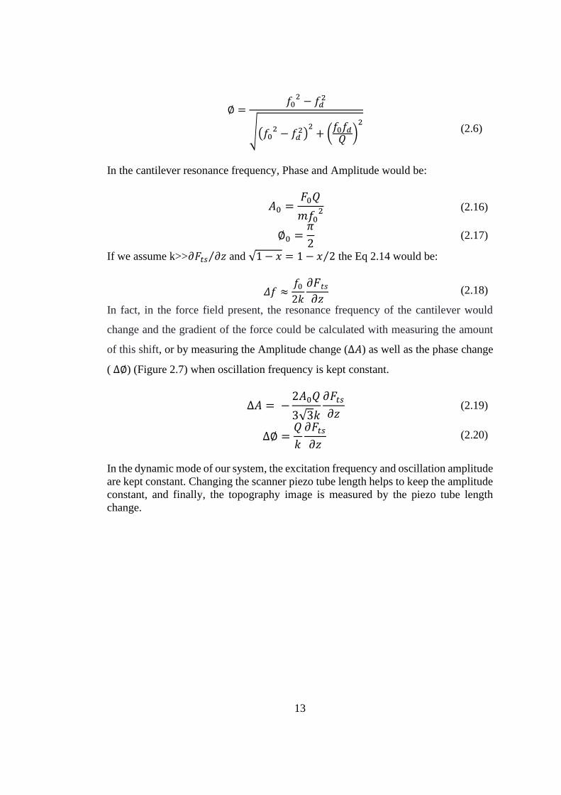
Figure 2. 7 The oscillation amplitude and phase versus frequency. The blue line
indicates cantilever oscillation amplitude in the free status and the red line is in the
condition which cantilever is brought to the surface and there is the force field
interaction. The first plot shows the amplitude which is decreased by ∆𝐴 and the
second plot corresponds to the phase shift ∆∅ . [49] ................................................. 14
Figure 2. 8 Lennard-Jones potential, strength vs distance ......................................... 16
Figure 2. 9 The graph represents the attractive and repulsive regime in Lennard-Jones
potential [50] .............................................................................................................. 17
Figure 3. 1Low-Temperature Atomic/Magnetic Force microscope Head with the Puk
and sample mounted. ................................................................................................. 20

xix
Figure 3. 2 1: holder, 2: zirconia tubing (ferrule) (0.050 g), 3: brass weight (1.5 g), 4:
leaf spring to hold the tubing, 5: V-shaped MFM holder 6: leaf spring for the
cantilever. ................................................................................................................... 21
Figure 3. 3 LT AFM/MFM Insert and Head. ............................................................ 22
Figure 3. 4 The connector head. ................................................................................ 22
Figure 3. 5 Expansion of the Piezoelectric disk due to the applied voltage.............. 23
Figure 3. 6 schematics of the Inner piezo tube with the electrode contacts. The dash
lines represent the piezo motion. (a) describes the four quadrants outside the tube wall
and motion in the x-y plane. (b) shows the five contacts which are conducted within
the inner piezo tube due to the scanning procedure in x, y, and Z directions. (c)
represents oscillatory motion for cantilever oscillation with a single electrode on the
top of the piezo tube. (d) the electrical contacts of a single oscillatory motion electrode,
given by Z'. [51] ......................................................................................................... 24
Figure 3. 7 The amount of the applied voltage to the scanner piezo tube quadrant. The
maximum voltage is between ± 100V. ....................................................................... 25
Figure 3. 8 3” scanner piezo tube calibration coefficients in different temperatures.
.................................................................................................................................... 27
Figure 3. 9 Schematic design of the slip-stick mechanism. [51] ............................. 28
Figure 3. 10 Exponential pulses applied to the slider piezo in order to displace the
holder.......................................................................................................................... 28
Figure 3. 11 Sample positioner and holders. [49] ..................................................... 29
Figure 3. 12 Mechanism for sample movement in X-Y direction with slider piezo for
sample positioning. The applied pulses to the AB-CD scanner piezo electrodes make
the sample displace in X-axis, and AD-BC electrode makes it move in Y-axis [53] 30
Figure 3. 13 Alignment holder schematic design...................................................... 31
Figure 3. 14 Cantilever Alignment holder chip and cantilever. ................................ 31
Figure 3. 15 Alignment holder of the cantilever in front of the fiber tubing ............ 32
Figure 3. 16 the Silicon made MFM cantilever scanning electron microscopy image
(SSS-MFMR). [60] .................................................................................................... 34
xx
Figure 3. 17 Schematic design of the interferometry method. The laser beam (I) go
through the fiber to the cantilever and part of that reflected from the fiber surface (Irs),
part of the rest beam again reflected from the cantilever (Irc) back to the source. The
df-c is fiber- cantilever distance.[51] ........................................................................... 34
Figure 3. 18 Michelson fiber interferometer schematic design. [49] ....................... 35
Figure 3. 19 Michelson Interferometer Interference pattern. The average slope is 4.27
mV/Å with visibility 0.27and at 327µWquadrature power. ...................................... 36
Figure 3. 20 LT-AFM control scheme.[51] ............................................................. 37
Figure 4. 1 schematic calculation size of the laser spot. [49] ................................... 39
Figure 4. 2 Cavity gap vs spot size diameter. ........................................................... 40
Figure 4. 3 sustaining the interference pattern in different temperatures represents the
durability of cantilever-tip durability (a) 300K, (b) 3K ............................................. 41
Figure 4. 4 Fiber Piezo capacitance change at the different Temperatures. ............. 42
Figure 4. 5 The fiber interferometer spectrum noise density at 300 K. .................... 45
Figure 4. 6 The laser power versus the noise density conducted in 300 K. .............. 46
Figure 4. 7 cantilever motion in tapping mode. [63] ................................................ 47
Figure 4. 8 Cantilever oscillation amplitude vs. drive frequency. [63] .................... 48
Figure 4. 9 (a) 3D image of Tapping mode Mika sample topography which is HF
etched and recorded at 3 K. (b) tapping mode topography image. (c) cross-section of
the image depicts the atomic single layer and multilayers steps. .............................. 49
Figure 4. 10 The Bluray disk sample topography image in tapping mode (a) at 300 K
(b) at 3 K .................................................................................................................... 50
Figure 4. 11 Magnetic stray field produced on the sample surface. [64] ................ 50
Figure 4. 12 Sony hi8 tape MFM images with different lift height parameters. (a) 80
nm, (b) 100 nm, (c) 120nm, (d) 150 nm .................................................................... 51
Figure 4. 13 Tip interaction in the magnetic field domain.[64]................................ 53
Figure 5. 1 The schematic description of the cryogenic temperatures. .................... 56
xxi
Figure 5. 2 The cryostat and gas handling system schematic design. [65] ............... 58
Figure 5. 3 (a) Stirling (b) G-M type BTR Schematics. 1.Compressor, 2. Aftercooler,
3. Regenerator, 4. Cold heat exchanger, 5. Pulse tube, 6. Hot heat exchanger, 7. Valve
[66] ............................................................................................................................. 60
Figure 5. 4 The inertance tube PTR schematic diagram. HHX: hot heat exchanger,
CHX: cold heat exchanger, 𝑄: 𝐻𝑒𝑎𝑡 𝑟𝑎𝑡𝑒, 𝑤: 𝑃𝑜𝑤𝑒𝑟 [𝑊], cp: Compressor,
𝑄ℎ: 𝐻𝑒𝑎𝑡 𝑡𝑟𝑎𝑛𝑠𝑓𝑒𝑟 𝑓𝑟𝑜𝑚 𝑡ℎ𝑒 ℎ𝑜𝑡 𝑒𝑛𝑑. [66] ........................................................... 62
Figure 5. 5 The schematic of the cryocooler working principal. [67]....................... 63
Figure 5. 6 (a) The cryostat, and (b) Isolation Vibration Platform. .......................... 63
Figure 5. 7 The vibration isolation table schematic design. (a), (b), and (c) are air
damping isolation legs, (d) is an edge welded bellows, (e) platform. ........................ 65
Figure 5. 8 The cable noise-canceling block, (a) Screwed position and (b) Parts. .. 66
Figure 5. 9 10 pm x 10 pm HOPG scan image with the cross-section when the stage
is off. .......................................................................................................................... 66
Figure 5. 10 Roughness parameters on the 10 pm x 10 pm HOPG image when the
stage is off. ................................................................................................................. 67
Figure 5. 11 10 pm x 10 pm HOPG scan image with the cross-section when the stage
is on. ........................................................................................................................... 67
Figure 5. 12 Roughness parameters on the 10 pm x 10 pm HOPG image when the
stage is on. .................................................................................................................. 67
Figure 5. 13 histogram FWHM analysis of the scanned 10 pm x10pm HOPG (a)
Vibration isolation platform is off, (b) Vibration Isolation platform is on. ............... 68
Figure 5. 14 AFM topography images of the iPhone camera chip in Tapping mode,
(a) 225 K, (b) 77 K, (C) 1.3 K. ................................................................................... 69
Figure 5. 15 Single-layer Graphene. ......................................................................... 70
Figure 6. 1The fiber Fabry-Perot interferometer (FFPI) Schematic principal. To
increases, the ratio of the internal reflection of the fiber and provides multiple
reflections between two parallel mirrors the fiber end should be coated. .................. 72
xxii
Figure 6. 2 Parts of the LT fiber slider. (a) MFM V-shaped holder, (b) ferrule tubing
made of Zirconia, and (c) PhBr Leaf spring. ............................................................. 74
Figure 6. 3(a) PPS holder, (b) Brass Weight (1.5 gr) ............................................... 75
Figure 6. 4 The V-shaped MFM holder schematic design which is assembled o top
of PPS part at the end of the scanner piezo tube for sliding mechanism. (b) Scanner
piezo, (c) Assembly of the microscope head. ............................................................ 75
Figure 6. 5 Fiber Approach by Stick-Slip Approach Mechanism. .......................... 76
Figure 6. 6Slider Piezo Step Length in 300K, 225K, 77K, 4K. (a) Forward motion,
(b) Backward motion. ................................................................................................ 77
Figure 6. 7 Measuring fiber step on the interference pattern at 300 K. A single step
with 300 V height slider pulse applied for approaching. The red plot is the interference
pattern of the fiber position after one step moved toward the cantilever which is
measured 74 nm displacement. .................................................................................. 78
Figure 6. 8 Slope and Visibility behavior vs gap distance between the cantilever and
fiber. ........................................................................................................................... 79
Figure 6. 9 fiber optic circulator diagram for fiber interferometer [64]. ................. 80
Figure 6. 10 schematic design of the fiber-cantilever reflectivity. 𝐸𝑖𝑛𝑐 , 𝐸𝑟 , 𝐸𝑠 are
respectively the incident beam, the fiber surface reflected beam, the summation of the
cantilever and fiber reflected beam, R1 fiber surface reflectivity, R2 cantilever
Reflectivity. ............................................................................................................... 81
Figure 6. 11 The Fabry-Pérot interferometer (Blue) and Michelson (Red) Modeling
for 1,310 nm wavelength. .......................................................................................... 83
Figure 6. 12 Different drive laser power in the Fibre Fabry-Perot interferometer at
300 K. ........................................................................................................................ 84
Figure 6. 13 Representation of the Linear relationship between the interference slope
& Average power at quadrature point Vs drive laser power @ 300K. ...................... 84
Figure 6. 14 AFM image of the grating sample in Tapping mode at 300 K. (a) Sample
Topography, (b) Amplitude (Feedback) and, (c) Phase images. ............................... 85
Figure 6. 15 AFM image of the Graphite in Tapping mode at 300 K. (a) Topography,
(b) Amplitude (Feedback). (c) Graphite layers size. ................................................. 86

xxiii
Figure 6. 16 AFM image of the Graphite in Tapping mode at 77 K. (a) Sample
Topography, (b) Amplitude (Feedback). (c) Graphite layers size. ............................ 87
Figure 6. 17 Tapping mode AFM image the Mika at 70 K. (a) Topography, (b)
Amplitude (Feedback). (c) Mika single layers. .......................................................... 88
Figure 6. 18 MFM image of the Sony hi8 type sample at 77 K: (a) Topography and
(b) Magnetic image. Lift-off amount was 100 nm. (c) Cross-section of the magnetic
image. ......................................................................................................................... 89
Figure 6. 19 MFM image of the 80 GB/Platter hard disk sample at 300 K: (a)
Topography and (b) Magnetic image. Lift-off amount was 85 nm............................ 90
Figure 6. 20 MFM image of out of plane magnetic field on the floppy disk surface
(a)Topography, (b) MFM image with 300 nm Lift-off value at 300K, (c, d) Cross
section of magnetic image measurements. ................................................................. 91
Figure 6. 21 Large laser bumps at the no load- unload ramps on the hard disk surface
also known as the landing zone for the head of the hard disk. (a, b) Topography, and
MFM image at 300 K, (c, d) Topography and MFM image at the 77 K. .................. 92
xxiv
LIST OF ABBREVIATIONS
ABBREVIATIONS
AC Alternating current AFM Atomic Force Microscope Co Co CoPt Cobalt platinum DC Direct current DOS Density of states DR Dilution refrigerator EFM Electrostatic Force Microscope Fe Iron
FFPI Fiber Fabry-Pérot interferometer
FWHM Full Width Half Maximum
FMR Frequency Modulation Reflective coating
GB Gigabit
GBP Gain bandwidth product
Gbpsi Giga bit per square inch
HF Hydrofluoric acid
HOPG Highly Ordered Pyrolytic Graphite 3He Helium three
ID Inner diameter
IR Infrared
ITO Indium tin oxide
I-V Current to voltage
IVC Inner vacuum jacket
K Kelvin
kHz Kilo Hertz
LT Low Temperature
LT-AFM/MFM Low Temperature Atomic Force
Microscope/Magnetic Force Microscope
MFM Magnetic Force Microscope
MFMR Magnetic Force Microscopy Reflective
coating
MHz Mega Hertz
mK milliKelvin
mbar milibar
NA Numerical aperture
nm Nanometer
Ni Nickel

xxv
OD Outside diameter
PCB Printed circuit board
PD Photodetector
PhBr Phosphor bronze
PID Proportional Integral Derivative
PLL Phase Lock Loop
SHPM Scanning Hall Probe Microscopy
SPM Scanning Probe Microscope
ss Stainless steel
STM Scanning Tunneling Microscope
SHO Simple harmonic oscillator
TL Top loading
VTI Variable temperature insert
V_PD Signal photodiode voltage

xxvi
LIST OF SYMBOLS
SYMBOLS
Symbols
A Amplitude
A0 The amplitude at the resonance frequency Å Angstrom Åpp Angstrom peak to peak BW Bandwidth
C Speed of light
D The outside diameter of the piezo tube
d Fiber-cantilever separation
d31 Transverse piezoelectric coefficient
E Magneto static energy
e Charge (1.6x10⁻¹⁹ C)
ε Thermal conductivity coefficient
emu Electromagnetic unit
F Force
Fts Tip-sample interaction force Fd(t) Driving force f0 Resonance frequency fm Femtometer
�⃗⃗� Magnetic stray field
Hc Critical field density
h Planck constant (6.63x10⁻³⁴ J.s)
i Photocurrent
i_shot Shot noise current
i0 Midpoint photocurrent
Jc Critical current density
k Spring constant
kB Boltzmann constant (1.38x10⁻²³ J/K)
kx Piezo coefficient in the x-axis ky Piezo coefficient in the y-axis Kz Piezo coefficient in the z-axis
L Length
�⃗⃗� Magnetization
NTotal_rms Summation of noises
m Mass
m Interference slope
ms Millisecond
�⃗⃗� Magnetic moment μ Micro

xxvii
μ0 Permeability of free space (4π x10-7H)
N Newton
n Refractive index
nrms Average mean square value of noise nm Number of moles np Number of photons nF Nano Farad
ns Nanosecond
Oe Oersted
P Optic power
p Pico
PRP The momentum of the light
Q Q-Factor
QTotal Total heat θ Half angle of the maximum cone of the light
R Reflectivity
RF Feedback resistor Rnumber Thermal conductivity S Spectral noise density
s Wall thickness of tube piezo
SPD The responsivity of the photodetector
T Temperature
T Tesla
TF Fermi temperature
t Time
U Applied voltage to the electrodes
z Position
Δx Lateral piezo displacement Δz Displacement Δf Frequency shift ΔA Amplitude shift ΔØ Phase shift Δl Length change ΔT Temperature difference
𝛻 Gradient
λ Wavelength α Thermal contraction coefficient
β Fabry-Pérot slope coefficient
𝜏 Optical path difference of the cavity gap z0 initial position, equilibrium position <z2> Mean square amplitude of the cantilever δF' A derivative of the force 𝜕𝑧
𝜕𝑡
A derivative of position with respect to time

xxviii
𝜕𝑉
𝜕𝑧
A derivative of potential energy with respect to the position
δ Damping factor Ø Phase V(z) Potential V Visibility �̅� Voltage noise v_shot shot Shot noise voltage ω Angular frequency W Watt Ω Ohm AC Alternating current AFM Atomic Force Microscope Co Cobalt CoPt Cobalt platinum DC Direct current DOS Density of states DR Dilution refrigerator EFM Electrostatic Force Microscope EI Experimental insert Fe Iron FFPI Fibre Fabry-Pérot interferometer FWHM Full-Width Half Maximum FMR Frequency Modulation Reflective coating GB Gigabit
GBP Gain bandwidth product Gbpsi Gigabit per square inch HF Hydrofluoric acid HOPG Highly Ordered Pyrolytic Graphite 3He Helium three
ID Inner diameter IR Infrared I-V Current to voltage IVC Inner vacuum jacket K Kelvin kHz Kilo Hertz LT Low Temperature LT-FM/MFM Low-Temperature Atomic Force Microscope/Magnetic Force
Microscope MFM Magnetic Force Microscope MFMR Magnetic Force Microscopy Reflective coating MHz MegaHertz mK milliKelvin mbar millibar NA Numerical aperture nm Nanometer
xxix
Ni Nickel OD Outside diameter PCB Printed circuit board PD Photodetector PhBr Phosphor bronze PID Proportional Integral Derivative PLL Phase Lock Loop PrFM Piezoresponse Force Microscopy RF Radiofrequency SHPM Scanning Hall Probe Microscopy SNR Signal to noise ratio SPM Scanning Probe Microscope ss Stainless steel SSS Super Sharp Silicon STM Scanning Tunneling Microscope SHO Simple harmonic oscillator TL Top loading VCO Voltage Controlled Oscillator VTI Variable temperature insert V_PD Signal photodiode voltage


1
CHAPTER 1
1. INTRODUCTION
1.1. Introduction and Overview
Atomic force microscopy (AFM), an innovative method that enables to map the
structures of the surface with fabulous resolution and precision. Images with a high
resolution of single atoms arrangement on the surface of a sample or the formations
of individual molecules are the fascinating capability of this microscopy method.
Imaging in a cryogenic temperature with an ultra-high vacuum provides the possibility
to measure a sample's surface properties with an atomic resolution [1]. Besides, not
necessarily AFM needs to be operated under this extreme condition; it can be
performed in the physiological buffers at 37 C to map biological reactions in real-time
[2-4]. Different kinds of samples like the surface of ceramic materials such as a very
hard one or distribution of metallic nanoparticles as well as very soft, like cells of the
human body, very flexible polymers, or DNA fragments could be carried out by the
AFM. The great advantages of this imaging method made it such a versatile
application since the 1980s which has employed to be utilized in all experimental
science areas like chemistry, physics, biology, material and nanotechnology science,
medicine, and etc. These days AFM is the most reliable technique to deliver highly
quantitative images with ultra-high resolution in the industrial, academic, and also
government labs.
An AFM microscope is rather varied from other microscopes which are operating with
light or electron focusing on a surface such as an optical or electron microscope. The
AFM is an almost mechanical technique and touches the material surface with a very
sharp probe, that maps the features as well as the height of the surface, in other words,
it projects the sample surface in three dimensions. The data provided by an AFM must

2
be analyzed by the software to generate the topography image, also analysis possibly
helps to remove artifacts from the surface of the image as well.
The first AFM (Figure 1.1) was a stylus profiler including a lever with optical
properties that could observe the movement of the lever with a tip at the end and a
small bar that was dragged through the surface of the sample and mapped the surface
topography. The common problem of this method was the probability of lever bending
due to the horizontal force made by surface large features. Becker presented this
problem [5] in 1950 and proposed to oscillate the lever in the initial state. The
vibration method somehow prevents the lever from bending, collapsing to the surface,
and damaging the sample.
Figure 1. 1Earliest design of the AFM with an optical lever in the 1920s. [6]
In 1971, the non-contact type of scanning probe microscopy was claimed by Russell
Young which made of a sharp metal probe and works with the electron field emission
current principal [7] in between the metal probe and the sample surface. He mounted
the sharp tip on the piezoelectric ceramic elements to move the Z direction.
Monitoring the probe motion in three directions (X, Y, and Z) provides the 3-
dimensional image of the sample surface.
In 1981 [8-10] Binnig and Rohrer tried to improve this method and apply the vibration
isolation. In such a way, it was possible to observe the tunneling of the electron rather
3
than electron emission among the tip and sample. This method was the first generation
of scanning tunneling microscopy (STM).
STM is able to measure individual atoms or molecules as well as measuring the local
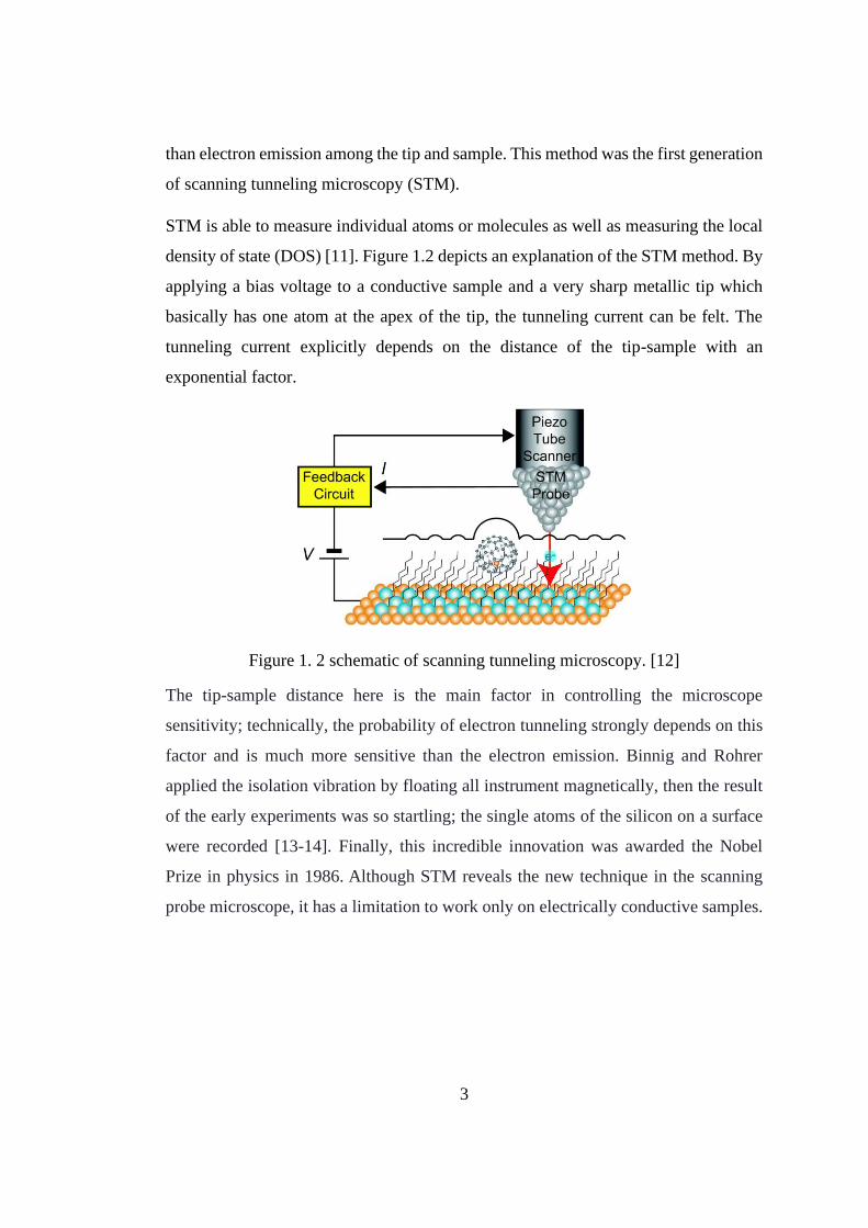
density of state (DOS) [11]. Figure 1.2 depicts an explanation of the STM method. By
applying a bias voltage to a conductive sample and a very sharp metallic tip which
basically has one atom at the apex of the tip, the tunneling current can be felt. The
tunneling current explicitly depends on the distance of the tip-sample with an
exponential factor.
Figure 1. 2 schematic of scanning tunneling microscopy. [12]
The tip-sample distance here is the main factor in controlling the microscope
sensitivity; technically, the probability of electron tunneling strongly depends on this
factor and is much more sensitive than the electron emission. Binnig and Rohrer
applied the isolation vibration by floating all instrument magnetically, then the result
of the early experiments was so startling; the single atoms of the silicon on a surface
were recorded [13-14]. Finally, this incredible innovation was awarded the Nobel
Prize in physics in 1986. Although STM reveals the new technique in the scanning
probe microscope, it has a limitation to work only on electrically conductive samples.

4
(a) (b)
Figure 1. 3 STM image, (a) Topography, (b) Size of the Graphite on the HOPG.
The invention of the AFM provides an opportunity not only to image conductive
samples but also image isolating samples. In AFM, distance dependency of the sample
and the tip plays a vital role in dominating either repulsive and attractive force
interaction. In AFM contact mode, the probe touches the sample surface and maps the
surface in the repulsive force regime. In the contact mode, the periodicity [15] and
lateral friction force [16] could be studied. By increasing the tip-sample distance, the
role of an attractive force is so essential, and in which the tip does not touches the
surface and in any contact with the surface of the sample, we can call AFM non-
contact mode [17]. Tapping mode or semi-contact mode [18] or phase image mode
[19] AFM works in both attractive and repulsive force regime, which is the commonly
used mode these days. The capability of measuring Magnetic, Electrostatic, friction,
or Van der Wall forces besides imaging the sample surface by utilizing the specific
tips are the advantages of AFM. These forces could be measured when the specific tip
is manufactured; for instance, for measuring the magnetic features of the material, the
tip should be coated by magnetic materials. This technique is named magnetic force
microscopy (MFM). Technically, the method's name obtained by the force name
which is measured in AFM.

5
Figure 1. 4 AFM image of the 200 nm Nickle Oxide coated on the glass
Magnetic force microscopy is one of the essential measurements in exposing the
magnetic properties of the material [20]. Moreover, this technique is comparatively
easy and typical like AFM measurement, which is performed in a variety of
environments like the large magnetic field [21], vacuum, low temperature and so on.
Magnetic imaging in different temperatures and the high magnetic field has a
significant role in vortex imaging or manipulation of vortices [22-29] in
superconductors, domain wall in ferromagnetic thin films [30-31], magnetic phase
separation [32-33], topological isolators [34].
Low-temperature AFM and MFM (LT-AFM/MFM) measurements have limitations
such as small spaces, approximately a few centimeters, inside the cryostats; hence
there is a limited description in the literature [35-36] specifically temperatures below
the 4K. Measuring the cantilever deflection is relatively hard and fiber interferometer
[37-39] is the logical and reliable method for this sort of measurements. Here the
cantilever should be aligned entirely concerning the fiber due to a thermal contraction
in the low temperature.
1.2. Work Plan
In the aforementioned thesis, the ultra-low noise, self-aligned low-temperature Fabry-
Perot AFM/MFM which is working based on fiber interferometer and temperature
range of 1.3 K to 300 K was redesigned and developed. In this type of microscope,
6
there is no need for optical alignment between the fiber and cantilever. Obtaining the
graphene single layer image represents the capability of reaching a high resolution.
Technically, we used Nanosensor alignment chip [60] to perform the alignment-free
system and very simplistic to operate. The design of the mechanical parts in LT Fabry-
Perot AFM/MFM was precisely engineered and tried to minimize the thermal
contraction of the material, and suitable for different temperature ranges. In the design
of the microscope, we attempted to eliminate all the unnecessary positioning
procedure mechanism to eliminate the complication as well as utilizing as less mass
as possible in order to make the microscope suitable for limited space inside the
cryostat and cooling the system with less power.
The principals and the theory of atomic force microscopy and magnetic force
microscopy operation are described in chapter 2. In chapter 3, LT Fabry-Perot
AFM/MFM instrumentation and a new design with all modification and operation
principles are described.
In chapter 4, the experiments at the low temperature and noise sources and
measurements are explained. And finally, AFM and MFM images are presented. The
Mika single layer at the low temperature presents the high functionality of the
microscope.
Chapter 5 is a description of the low-temperature dry cryostat which is newly installed
in our lab with the capability of working in 1.3 K. Moreover, an isolation vibration
platform is designed to decrease the noise. The value of noise in both on and off status
of isolation platform is measured and incredibly we were able to image the single-
layer graphene while microscope inside the cryostat and pulse tube cold head working.
In chapter 6, the Fabry-Perot interferometry principle is described as well as the
modified mechanism of fiber movement to reach the Fabry- Perot basics and increase
the resolution based on increasing the laser power gain. And at the end, this
mechanism is tested at low temperature and the reliability of working in various
temperature ranges is proved.
7
CHAPTER 2
2. MAGNETIC FORCE MICROSCOPY
2.1. Magnetic Force Microscopy (MFM)
MFM is one of the AFM sub-branches with the potential of measuring magnetic
features of the sample which is soon realized in AFM history [40-42]. In MFM
measurements, it is so significant that the probe stays in very close distance to the
surface as magnetic stray field decays promptly with the distance factor. To obtain the
magnetic image, the probe should be magnetically coated to feel the distribution of
direct magnetic stray field above the surface. Typically, the probe consists of same
AFM silicon cantilever which is coated by a thin layer of magnetic material. The
typical materials which could be utilized for MFM cantilever are cobalt, cobalt-nickel
and cobalt -chromium [43]. Coating the cantilever due to magnetization brings
detrimental effects, firstly increasing the tip radius which decreases the resolution,
secondly increasing the wear rate as these materials are softer than the silicon itself.
Normally, on the sample surface, magnetic forces are being measured in certain
distance respect to the surface (of the order of approximately a few to a few hundreds
of nm). There are also some techniques to measure magnetic forces which particularly
have pros and cons. In "lifting"-type methods, firstly the topography is measured and
in the following by raising up in a certain amount, the cantilever can feel and measure
the magnetic forces.
One method is mapping the surface topography and then set a z set point to raise the
tip and collect the magnetic image. This method works in a flat surface and possibly
the thermal drift effects the MFM image (Figure 2.1).
8
Figure 2. 1 lifting the tip of the surface. [6]
Bard [44] mentioned an improved method, which firstly records the sample surface
topography, then by lifting the probe in a certain height and following the same
topography collects the MFM image (Figure 2.2). In this method, the probe scans a
surface in the forward and backward lines. In the forward scan, topography image is
collected, then in the backward line with a fixed lift, MFM image is being measured.
Figure 2. 2 schematic descriptions of the Bard method. [6]

9
In the other method, the probe changes the height in the Z direction during the scan,
in the other word, it will be continually shifting toward the sample to check the
topography and away to see the magnetic field (Figure 2.3).
Figure 2. 3 z set-point oscillation. [6]
Finally, according to Hosaka's description [45] at every pixel, the tip is raised above
the sample surface to record the magnetic field in various heights then it moves to the
next side points, lifted again and repeats. Although this method is slow, it can reduce
thermal drift effects (Figure 2.4).
Figure 2. 4Schematic descriptions of the Hosaka method. [6]
10
Typically, the MFM measurements are conducted in one of these dynamic modes and
the phase images expose the magnetic effects.
(a) (b)
Figure 2. 5 MFM image of the Sony hi8 tape which is conducted in 300K.
Topography (a) image is recorded by a forward scan and backward is used to record
the magnetic image (b).
2.1.1. Applicability
Magnetic force microscopes are of prime importance in scientific and industrial fields.
Particularly, the data storage industry relays on this accurate technique to investigate
the magnetic nanodomains of the hundred nanometers size range [46-47]. Study of
magnetic nanoparticles is the other tense interest within the scientific society which
MFM has a great use [48].
2.2. Operation Theory
AFM imaging measurement is operated in different ways which can be listed in two
parts: Static mode and Dynamic mode. The Dynamic mode itself divided in two: semi-
contact mode (which is called tapping mode) and non-contact mode.
2.2.1. Dynamic Mode
The cantilever in the dynamic mode is oscillating at its own resonance frequency with
utilizing a Piezo actuator. This motion can be modeled resemblance to a simple

11
harmonic oscillator in a spring-mass system (Figure 2.6) and solved by Newton's 2nd
low of motion.
𝐹 = 𝑚𝑎 = 𝑚𝜕2𝑧
𝜕𝑡2= −𝑘(𝑧 − 𝑧0)
(2.1)
𝑚𝜕2𝑧
𝜕𝑡2+ 𝑘(𝑧 − 𝑧0) = 0
(2.2)
𝑓0 ≡ √𝑘
𝑚
(2.3)
Respectively k, m, and 𝑓0 are cantilever spring constant, mass, and natural resonance
frequency. In the absence of the force field, 𝑧0 is the cantilever position, and z is
distance among the sample surface and the cantilever apex.
Figure 2. 6 The schematic resemblance of a spring-mass system and cantilever. [49]
Including the friction force, the oscillatory system can be described by a damped
harmonic oscillator:
𝑚𝜕2𝑧
𝜕𝑡2+ 𝛿
𝜕𝑧
𝜕𝑡+ 𝑘(𝑧 − 𝑧0) = 0 (2.4)
𝛿 =𝑘
𝑓0𝑄 (2.5)
Where 𝛿 is damping factor and Q is the quality factor.
12
In the presence of a driving force provided by Piezo actuator:
𝐹𝑑(𝑡) = 𝐹0 cos𝜔𝑡 (2.6)
⇒ 𝑚𝜕2𝑧
𝜕𝑡2+ 𝛿
𝜕𝑧
𝜕𝑡+ 𝑘(𝑧 − 𝑧0) = 𝐹𝑑(𝑡)
(2.7)
By including the tip-sample interaction the equation would be:
⇒ 𝑚𝜕2𝑧
𝜕𝑡2+ 𝛿
𝜕𝑧
𝜕𝑡+ 𝑘(𝑧 − 𝑧0) = 𝐹𝑑(𝑡) + 𝐹𝑡𝑠(𝑧)
(2.8)
The tip-sample term makes non-linearity in the equation. Therefore, 𝐹𝑡𝑠(𝑧) should be
expanded by a Taylor series:
𝐹𝑡𝑠(𝑧) = 𝐹𝑡𝑠(𝑧0) +𝜕𝐹𝑡𝑠(𝑧0)
𝜕𝑧(𝑧 − 𝑧0)
(2.9)
Approximately, 𝐹𝑡𝑠 is equal in these two terms with enough oscillation amplitude and
small interaction force.
𝑚𝜕2𝑧
𝜕𝑡2+ 𝛿
𝜕𝑧
𝜕𝑡+ 𝑘(𝑧 − 𝑧0) = 𝐹𝑑(𝑡) + 𝐹𝑡𝑠(𝑧0) +
𝜕𝐹𝑡𝑠𝜕𝑧|𝑧=𝑧0(𝑧 − 𝑧0)
(2.1)
⇒ 𝑚𝜕2𝑧
𝜕𝑡2+ 𝛿
𝜕𝑧
𝜕𝑡+ [𝑘 −
𝜕𝐹𝑡𝑠𝜕𝑧|𝑧=𝑧0](𝑧 − 𝑧0) = 𝐹𝑑(𝑡) + 𝐹𝑡𝑠(𝑧0)
(2.2)
The term 𝑘 −𝜕𝐹𝑡𝑠
𝜕𝑧 is called effective spring constant, 𝑘𝑒𝑓𝑓.
The above differential equation solution can be written as:
𝑧(𝑡) = 𝑧0 + 𝐴 cos(2𝜋𝑓𝑑𝑡 − ∅) (2.3)
And
𝑓𝑑 = √𝑘
𝑚−1
𝑚
𝜕𝐹𝑡𝑠𝜕𝑧
(2.4)
𝐴 =
𝐴0𝑚⁄
√(𝑓02 − 𝑓𝑑
2)2+ (𝑓0𝑓𝑑𝑄)2
(2.5)
13
∅ =𝑓02 − 𝑓𝑑
2
√(𝑓02 − 𝑓𝑑
2)2+ (𝑓0𝑓𝑑𝑄)2
(2.6)
In the cantilever resonance frequency, Phase and Amplitude would be:
𝐴0 =𝐹0𝑄
𝑚𝑓02 (2.16)
∅0 =𝜋
2 (2.17)
If we assume k>>𝜕𝐹𝑡𝑠 𝜕𝑧⁄ and √1 − 𝑥 = 1 − 𝑥 2⁄ the Eq 2.14 would be:
𝛥𝑓 ≈𝑓02𝑘
𝜕𝐹𝑡𝑠𝜕𝑧
(2.18)
In fact, in the force field present, the resonance frequency of the cantilever would
change and the gradient of the force could be calculated with measuring the amount
of this shift, or by measuring the Amplitude change (∆𝐴) as well as the phase change
( ∆∅) (Figure 2.7) when oscillation frequency is kept constant.
∆𝐴 = −2𝐴0𝑄
3√3𝑘
𝜕𝐹𝑡𝑠𝜕𝑧
(2.19)
∆∅ =𝑄
𝑘
𝜕𝐹𝑡𝑠𝜕𝑧 (2.20)
In the dynamic mode of our system, the excitation frequency and oscillation amplitude
are kept constant. Changing the scanner piezo tube length helps to keep the amplitude
constant, and finally, the topography image is measured by the piezo tube length
change.
14
Figure 2. 7 The oscillation amplitude and phase versus frequency. The blue line
indicates cantilever oscillation amplitude in the free status and the red line is in the
condition which cantilever is brought to the surface and there is the force field
interaction. The first plot shows the amplitude which is decreased by ∆𝐴 and the
second plot corresponds to the phase shift ∆∅ . [49]
2.2.2. Static Mode
Almost the probe is like a spring which in interaction with the surface could be bend.
This force is explained by Hook’s low.
∆𝑍 =𝐹𝑡𝑠𝑘
(2.27)

15
Here ∆𝑍 is the amount of the displacement, k is the cantilever spring constant and 𝐹𝑡𝑠
is the sample-cantilever interaction force. By measuring the cantilever deflection,
accordingly, the force could be calculated. This method is not suitable for MFM
measurements. In this mode, the cantilever always is in contact with the surface in
contact with the sample surface and its sensitivity is poor.
2.2.3. Tip-Sample Magnetic Interaction
As it previously discussed MFM measurements is conducted between a magnetic
sample and a magnetic cantilever, therefore, the total magnetostatics energy would be:
𝐸 = −𝜇02[∫ �⃗⃗� 𝑡𝑖𝑝�⃗⃗� 𝑆𝑎𝑚𝑝𝑙𝑒𝑑𝑉 +∫ �⃗⃗� 𝑡𝑖𝑝�⃗⃗� 𝑆𝑎𝑚𝑝𝑙𝑒𝑑𝑉] (2.22)
�⃗⃗� = ∫ �⃗⃗� 𝑑𝑉 (2.23)
Where H is a stray field, M magnetization, m magnetic moment, and 𝜇0 Permeability
of free space.
As the two integrals are equal, the energy equation would be:
𝐸 = −𝜇0 [∫ �⃗⃗� 𝑡𝑖𝑝�⃗⃗� 𝑆𝑎𝑚𝑝𝑙𝑒𝑑𝑉] (2.24)
Over the surface scan, the cantilever displaces only in the vertical direction, hence, we
need to consider the vertical magnetic component of the force.
𝐹𝑡𝑠(𝑧) = −∇E = 𝜇0 ∫ ∇(�⃗⃗� 𝑡𝑖𝑝�⃗⃗� 𝑆𝑎𝑚𝑝𝑙𝑒)𝑑𝑉𝑡𝑖𝑝𝑉𝑡𝑖𝑝
(2.25)
𝐹𝑡𝑠(𝑧) = 𝜇0 ∫ �⃗⃗� 𝑡𝑖𝑝𝜕�⃗⃗� 𝑆𝑎𝑚𝑝𝑙𝑒
𝜕𝑧𝑑𝑉𝑡𝑖𝑝
𝑉𝑡𝑖𝑝
(2.26)
𝜕𝐹𝑡𝑠𝜕𝑧
= 𝜇0 ∫ �⃗⃗� 𝑡𝑖𝑝𝜕2�⃗⃗� 𝑆𝑎𝑚𝑝𝑙𝑒
𝜕𝑧2𝑑𝑉𝑡𝑖𝑝
𝑉𝑡𝑖𝑝
(2.27)
2.2.4. Lennard-Jones Potential

16
A couple of natural atoms or molecules interaction can be mathematically modeled by
Lennard-Jones Potential. Here this method is employed in Tip-Sample interaction.
𝑉𝐿𝐽 = 4휀 [(𝜎
𝑟)12
− (𝜎
𝑟)6
] = 휀 [(𝑟𝑚𝑟)12
− 2(𝑟𝑚𝑟)6
] (2.28)
where r, 𝜎, 휀, and 𝑟𝑚 are the distance between the particle, the finite distance at which
the potential of inter-particle is zero, the potential well depth, and the distance which
the potential reaches its minimum respectively. At the 𝑟𝑚 the potential would be −휀.
(Figure 2.8)
Figure 2. 8 Lennard-Jones potential, strength vs distance
The repulsive force term is defined by the term 𝑟−12 ; the Pauli repulsion when
electron orbitals overlap in the short, and attractive long-term range is defined with
the term 𝑟−6 to depict long term attractions like dispersion or Van der Waals force.
[49]
The form which is simplified for software simulations is:
𝑉𝐿𝐽 =𝐴
𝑟12−𝐵
𝑟6 (2.29)
Where 𝐴 = 4휀𝜎12 and B= 4휀𝜎6
17
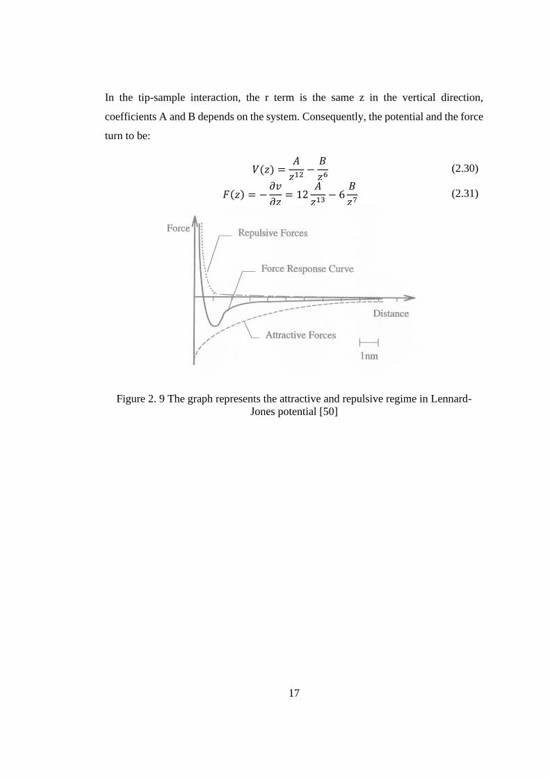
In the tip-sample interaction, the r term is the same z in the vertical direction,
coefficients A and B depends on the system. Consequently, the potential and the force
turn to be:
𝑉(𝑧) =𝐴
𝑧12−𝐵
𝑧6 (2.30)
𝐹(𝑧) = −𝜕𝑣
𝜕𝑧= 12
𝐴
𝑧13− 6
𝐵
𝑧7 (2.31)
Figure 2. 9 The graph represents the attractive and repulsive regime in Lennard-
Jones potential [50]

19
CHAPTER 3
3. MICROSCOPE INSTRUMENTATION
3.1. Microscope Instrumentation
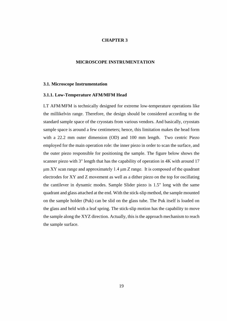
3.1.1. Low-Temperature AFM/MFM Head
LT AFM/MFM is technically designed for extreme low-temperature operations like
the millikelvin range. Therefore, the design should be considered according to the
standard sample space of the cryostats from various vendors. And basically, cryostats
sample space is around a few centimeters; hence, this limitation makes the head form
with a 22.2 mm outer dimension (OD) and 100 mm length. Two centric Piezo
employed for the main operation role: the inner piezo in order to scan the surface, and
the outer piezo responsible for positioning the sample. The figure below shows the
scanner piezo with 3" length that has the capability of operation in 4K with around 17
μm XY scan range and approximately 1.4 μm Z range. It is composed of the quadrant
electrodes for XY and Z movement as well as a dither piezo on the top for oscillating
the cantilever in dynamic modes. Sample Slider piezo is 1.5" long with the same
quadrant and glass attached at the end. With the stick-slip method, the sample mounted
on the sample holder (Puk) can be slid on the glass tube. The Puk itself is loaded on
the glass and held with a leaf spring. The stick-slip motion has the capability to move
the sample along the XYZ direction. Actually, this is the approach mechanism to reach
the sample surface.
20
Figure 3. 1Low-Temperature Atomic/Magnetic Force microscope Head with the
Puk and sample mounted.
3.1.2. LT-AFM/MFM head design optimization
The most crucial aspect here is the mechanism for aligning the fiber and cantilever as
there is a particular danger of collisions during cooling due to thermal contraction.
Here, a concentric design helps to prevent any failure. Furthermore, both the size and
the thermal mass of the microscope head should be minimized to reduce the time
required for cooling and to meet the rigorous space limitations inside the cryostat.
Therefore, it is tried to reduce the thermal mass of the microscope head as much as
possible. For instance, some pieces were made of plastic (Polyphenylene sulfide
(PPS)) (Figure. 3.2, part 1). Furthermore, I increased the inertial mass of the brass
weight (Figure. 3.2, part 3) that holds the zirconia tubing that acts as ferrule (Figure.
3.2, part 2) to improve the reliability of the Nanopositioner in the wide range of
working temperatures from room temperature down to 1.3 K. Moreover, regarding the
space limitations inside the cryostat, I have strived to design the microscope head to
remain within 22.2 mm the outside diameter, and below 100 mm length to fit inside
the 30 mm diameter standard helium cryostats. Thereby, our microscope head is
compatible with various commercial cryostat designs.
Slider Piezo
Scanner Piezo
Glass Tube
Puk Piezo Holders Sample
21
Figure 3. 2 1: holder, 2: zirconia tubing (ferrule) (0.050 g), 3: brass weight (1.5 g),
4: leaf spring to hold the tubing, 5: V-shaped MFM holder 6: leaf spring for the
cantilever.
Technically all these designs are manufactured as a holder alignment and mounted on
the top of the scanner piezo. Figure 3.2, part 7, shows the schematic design of all parts
mounted together.
Therefore, the design is modified and results in improved reliability of the fiber
Nanopositioner. This was achieved by (1) centering the AFM tip at the piezo tube; (2)
improving the surface quality of the groves in which the ferrule is sliding; (3)
increasing the inertial mass of the fiber holder.
3.1.3. Microscope Insert
The LT AFM/MFM is divided into two main part, the head and insert. The inset part
is detachable from the docking part to the microscope head which provides the
compatibility to various types of cryostats as well as using different heads like AFM,
SHPM, STM, etc (Figure 3.3). The variable-length makes it possible to arrange the
microscope in the center of the cryostat in order to adjust in the center of magnetic
1
3 4
5
2
6
7
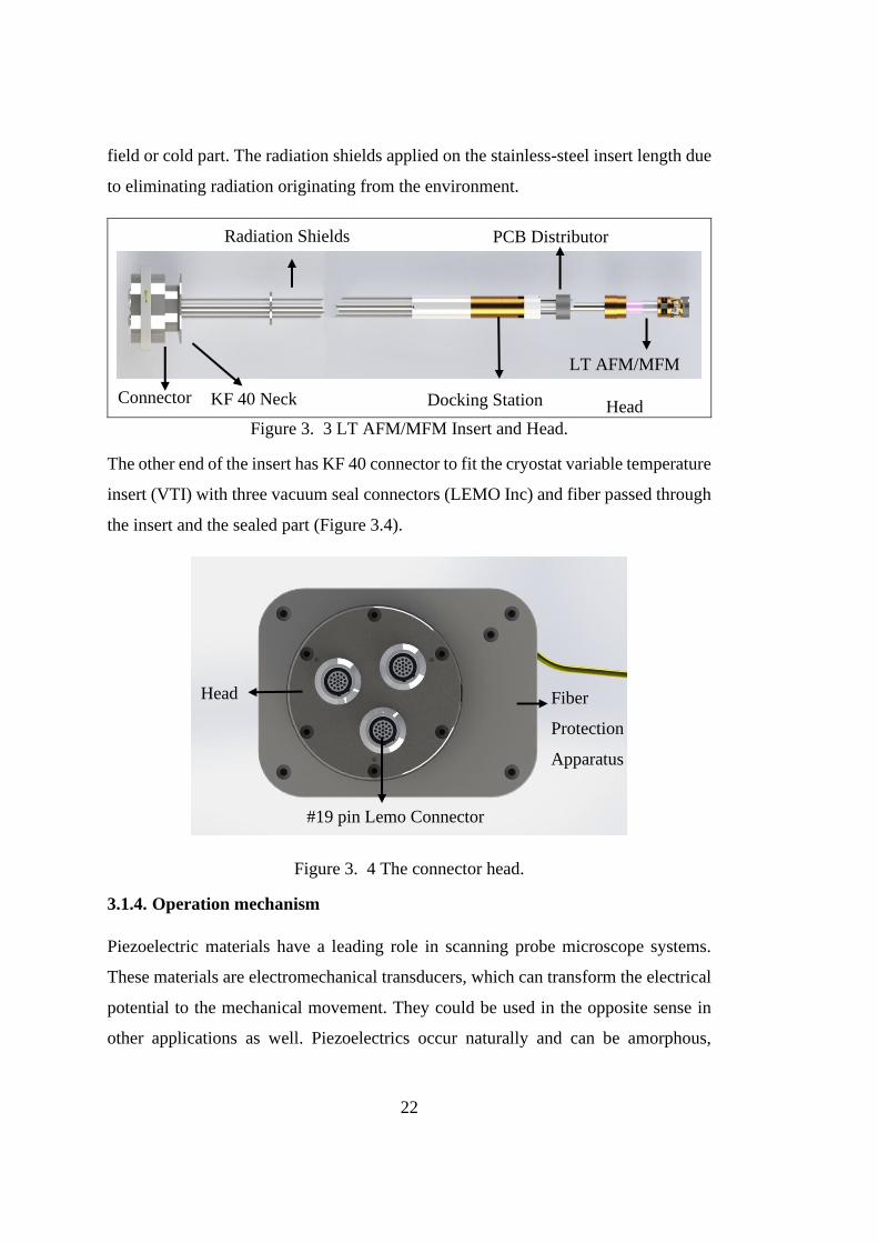
22
field or cold part. The radiation shields applied on the stainless-steel insert length due
to eliminating radiation originating from the environment.
Figure 3. 3 LT AFM/MFM Insert and Head.
The other end of the insert has KF 40 connector to fit the cryostat variable temperature
insert (VTI) with three vacuum seal connectors (LEMO Inc) and fiber passed through
the insert and the sealed part (Figure 3.4).
Figure 3. 4 The connector head.
3.1.4. Operation mechanism
Piezoelectric materials have a leading role in scanning probe microscope systems.
These materials are electromechanical transducers, which can transform the electrical
potential to the mechanical movement. They could be used in the opposite sense in
other applications as well. Piezoelectrics occur naturally and can be amorphous,
LT AFM/MFM
Head Docking Station
PCB Distributor Radiation Shields
Connector KF 40 Neck
Fiber
Protection
Apparatus
#19 pin Lemo Connector
Head

23
polymeric, and crystalline. In AFM applications, mostly synthetic ceramic materials
are used. Due to applied voltages to the opposite side electrodes of the piezoelectric
devices, the geometry would alter based on the amplitude of the applied voltage,
material, and device geometry. (Figure 3.5)
Figure 3. 5 Expansion of the Piezoelectric disk due to the applied voltage.
Technically, these materials have a specific coefficient of expansion with an order of
around 0.1 nm by each drive volt, which makes entirely controllable tiny movements
for AFM systems. When Piezo materials are under mechanical tension, the strength of
the electric polarity would be altered. This phenomenon is called the 'direct' effect of
piezoelectric. In reverse, if an electric field is applied due to unit cell distortion,
material changes its shape, which is called 'transverse' piezoelectric effect. As it is
mentioned, the piezoelectric ceramics ideally should expand in a linear regime and
contact in a direct proportion to the applied voltage, but unfortunately, all these
materials show some non-linear behavior. The first problem is hysteresis, in which the
piezo tube tends to maintain the previous shape. And on the other hand, imposing the
sudden impulse such a voltage step function to the ceramic makes creep.
The piezo tube used in LT AFM/MFM microscope is made by lead zirconium with
four-quadrant electrodes outside the wall and one single electrode inside. When two
reciprocal quadrants with grounded inner electrodes are under the opposite applied
voltage, the piezo tube will bend in X-Y planes (Figure 3.6). Accordingly, applying
the reverse voltage to all four quadrants, regarding the inner electrode, provides Z
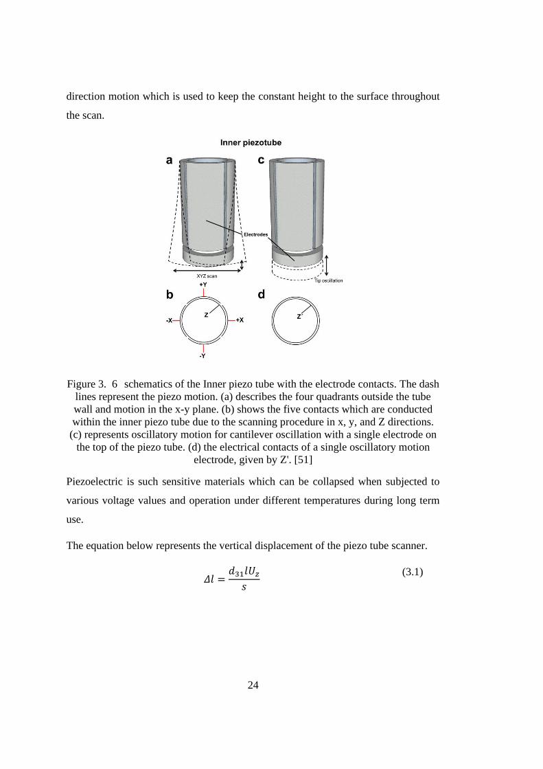
24
direction motion which is used to keep the constant height to the surface throughout
the scan.
Figure 3. 6 schematics of the Inner piezo tube with the electrode contacts. The dash
lines represent the piezo motion. (a) describes the four quadrants outside the tube
wall and motion in the x-y plane. (b) shows the five contacts which are conducted
within the inner piezo tube due to the scanning procedure in x, y, and Z directions.
(c) represents oscillatory motion for cantilever oscillation with a single electrode on
the top of the piezo tube. (d) the electrical contacts of a single oscillatory motion
electrode, given by Z'. [51]
Piezoelectric is such sensitive materials which can be collapsed when subjected to
various voltage values and operation under different temperatures during long term
use.
The equation below represents the vertical displacement of the piezo tube scanner.
𝛥𝑙 =𝑑31𝑙𝑈𝑧𝑠
(3.1)
25
Here the 𝑑31is transverse coefficient, l tube length, 𝑈𝑧The electrodes employed
voltage and s the tube wall thickness. Values for 𝑑31 @ 300 𝐾 𝑖𝑠 − 1.73 Å/𝑉, 𝑈𝑧 is
100 V, l is 3 inch, and s is 0.5 mm.
Also, the piezoelectric lateral displacement can be calculated:
𝛥𝑥 =2√2𝑑31𝑙
2𝑈𝑧𝜋𝐷𝑡
(3.2)
D denotes the otter dimension of the piezo tube with 6.35 mm.
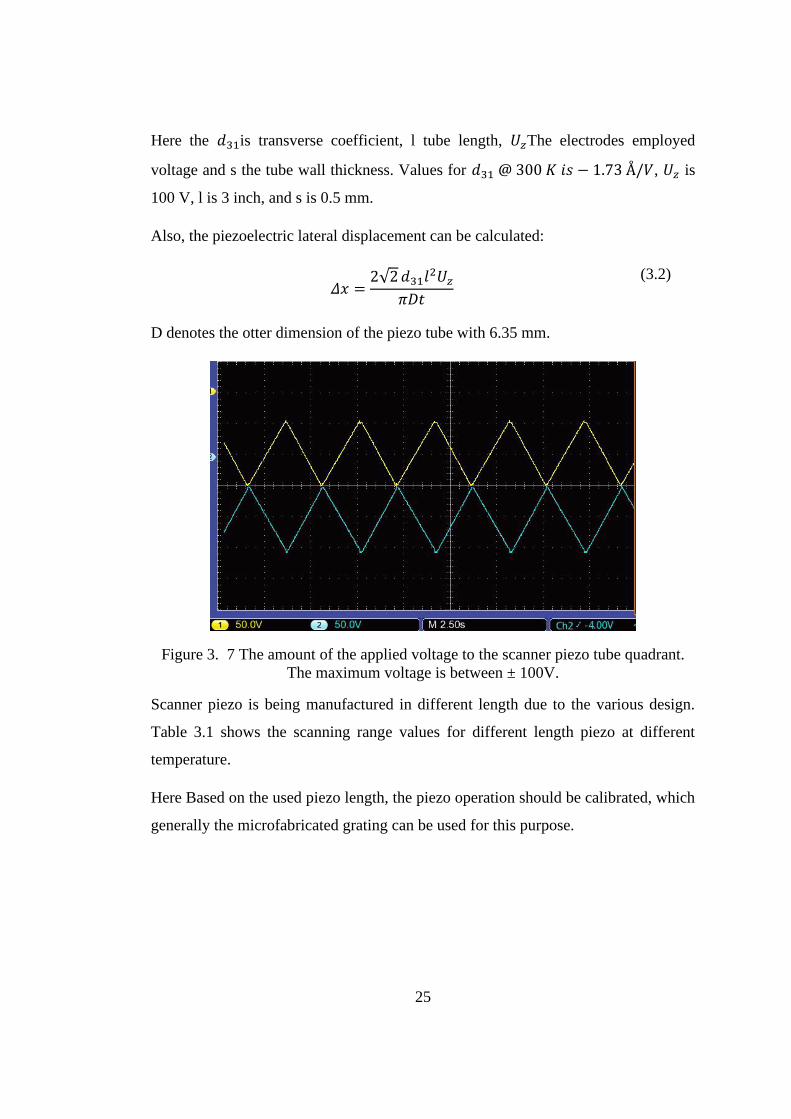
Figure 3. 7 The amount of the applied voltage to the scanner piezo tube quadrant.
The maximum voltage is between ± 100V.
Scanner piezo is being manufactured in different length due to the various design.
Table 3.1 shows the scanning range values for different length piezo at different
temperature.
Here Based on the used piezo length, the piezo operation should be calibrated, which
generally the microfabricated grating can be used for this purpose.
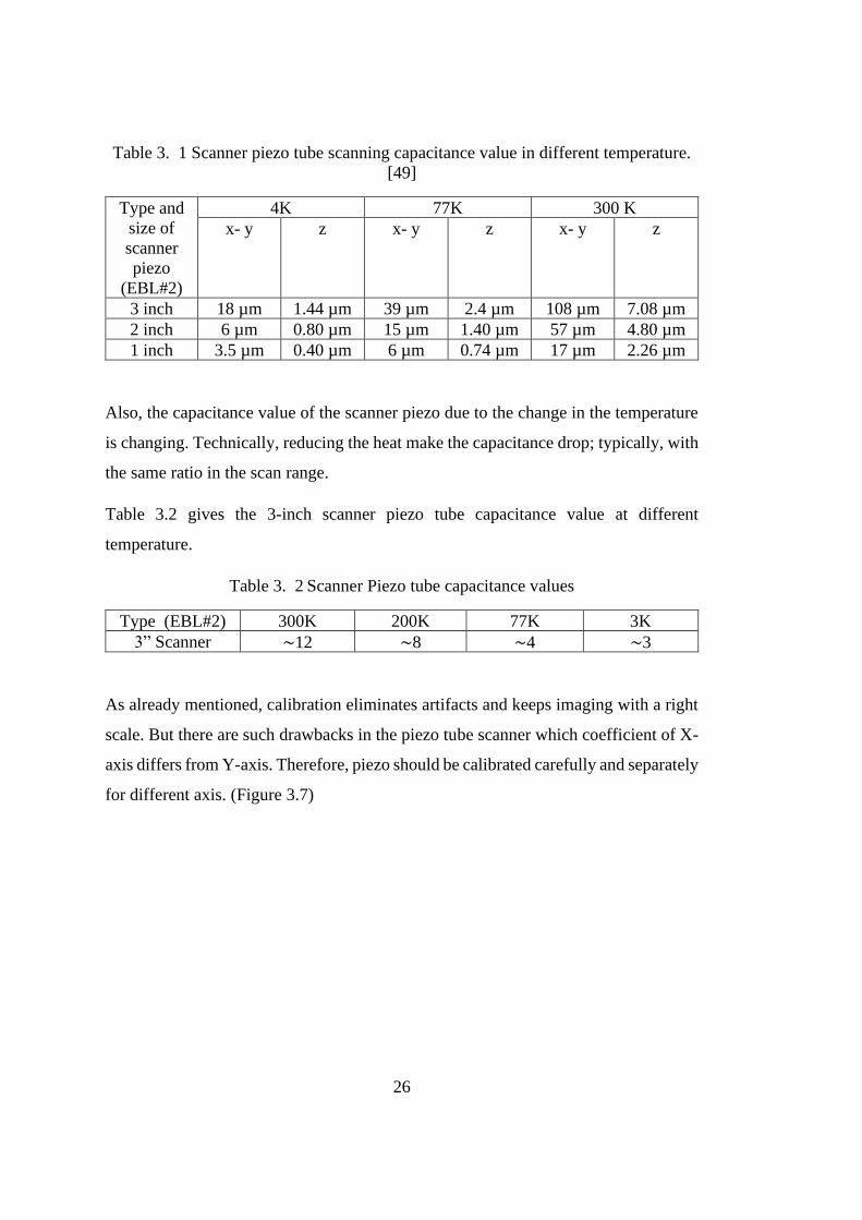
26
Table 3. 1 Scanner piezo tube scanning capacitance value in different temperature.
[49]
Type and
size of
scanner
piezo
(EBL#2)
4K 77K 300 K
x- y z x- y z x- y z
3 inch 18 µm 1.44 µm 39 µm 2.4 µm 108 µm 7.08 µm
2 inch 6 µm 0.80 µm 15 µm 1.40 µm 57 µm 4.80 µm
1 inch 3.5 µm 0.40 µm 6 µm 0.74 µm 17 µm 2.26 µm
Also, the capacitance value of the scanner piezo due to the change in the temperature
is changing. Technically, reducing the heat make the capacitance drop; typically, with
the same ratio in the scan range.
Table 3.2 gives the 3-inch scanner piezo tube capacitance value at different
temperature.
Table 3. 2 Scanner Piezo tube capacitance values
Type (EBL#2) 300K 200K 77K 3K
3” Scanner ~12 ~8 ~4 ~3
As already mentioned, calibration eliminates artifacts and keeps imaging with a right
scale. But there are such drawbacks in the piezo tube scanner which coefficient of X-
axis differs from Y-axis. Therefore, piezo should be calibrated carefully and separately
for different axis. (Figure 3.7)
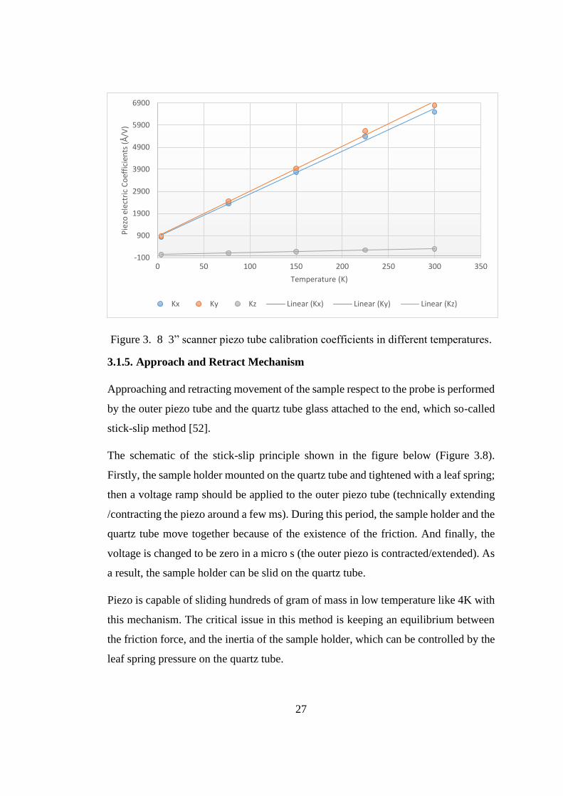
27
Figure 3. 8 3” scanner piezo tube calibration coefficients in different temperatures.
3.1.5. Approach and Retract Mechanism
Approaching and retracting movement of the sample respect to the probe is performed
by the outer piezo tube and the quartz tube glass attached to the end, which so-called
stick-slip method [52].
The schematic of the stick-slip principle shown in the figure below (Figure 3.8).
Firstly, the sample holder mounted on the quartz tube and tightened with a leaf spring;
then a voltage ramp should be applied to the outer piezo tube (technically extending
/contracting the piezo around a few ms). During this period, the sample holder and the
quartz tube move together because of the existence of the friction. And finally, the
voltage is changed to be zero in a micro s (the outer piezo is contracted/extended). As
a result, the sample holder can be slid on the quartz tube.
Piezo is capable of sliding hundreds of gram of mass in low temperature like 4K with
this mechanism. The critical issue in this method is keeping an equilibrium between
the friction force, and the inertia of the sample holder, which can be controlled by the
leaf spring pressure on the quartz tube.
-100
900
1900
2900
3900
4900
5900
6900
0 50 100 150 200 250 300 350
Pie
zo e
lect
ric
Co
effi
cien
ts (
Å/V
)
Temperature (K)
Kx Ky Kz Linear (Kx) Linear (Ky) Linear (Kz)
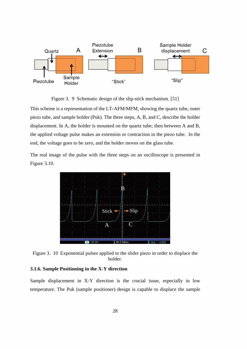
28
Figure 3. 9 Schematic design of the slip-stick mechanism. [51]
This scheme is a representation of the LT-AFM/MFM, showing the quartz tube, outer
piezo tube, and sample holder (Puk). The three steps, A, B, and C, describe the holder
displacement. In A, the holder is mounted on the quartz tube; then between A and B,
the applied voltage pulse makes an extension or contraction in the piezo tube. In the
end, the voltage goes to be zero, and the holder moves on the glass tube.
The real image of the pulse with the three steps on an oscilloscope is presented in
Figure 3.10.
Figure 3. 10 Exponential pulses applied to the slider piezo in order to displace the
holder.
3.1.6. Sample Positioning in the X-Y direction
Sample displacement in X-Y direction is the crucial issue, especially in low
temperature. The Puk (sample positioner) design is capable to displace the sample
A
B
C
V
C
V C
Slip
CVCV
Stick
CVCV

29
holder in a 3 mm diameter. The holder is responsible for holding the sample which is
loaded via five pins on the Puk. One pin is for sample bias, and the rest are spare. The
holder itself fiber-cantilever on the two couple parallel Zirconia rales, which one
couple is in the X direction and another one is in the Y direction. These rails are placed
on V-shape grooves beneath the sample holder and let the holder move in X and Y
directions.
The sample holder displacement at the orthogonal directions is handled by the slider
piezo. An applied high voltage to two neighbor quadrant couples concerning the
opposite couples’ quadrant provides the expected motion.
Figure 3. 11 Sample positioner and holders. [49]
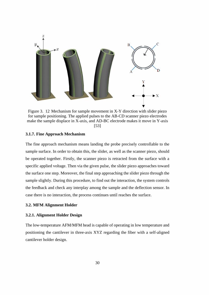
30
Figure 3. 12 Mechanism for sample movement in X-Y direction with slider piezo
for sample positioning. The applied pulses to the AB-CD scanner piezo electrodes
make the sample displace in X-axis, and AD-BC electrode makes it move in Y-axis
[53]
3.1.7. Fine Approach Mechanism
The fine approach mechanism means landing the probe precisely controllable to the
sample surface. In order to obtain this, the slider, as well as the scanner piezo, should
be operated together. Firstly, the scanner piezo is retracted from the surface with a
specific applied voltage. Then via the given pulse, the slider piezo approaches toward
the surface one step. Moreover, the final step approaching the slider piezo through the
sample slightly. During this procedure, to find out the interaction, the system controls
the feedback and check any interplay among the sample and the deflection sensor. In
case there is no interaction, the process continues until reaches the surface.
3.2. MFM Alignment Holder
3.2.1. Alignment Holder Design
The low-temperature AFM/MFM head is capable of operating in low temperature and
positioning the cantilever in three-axis XYZ regarding the fiber with a self-aligned
cantilever holder design.
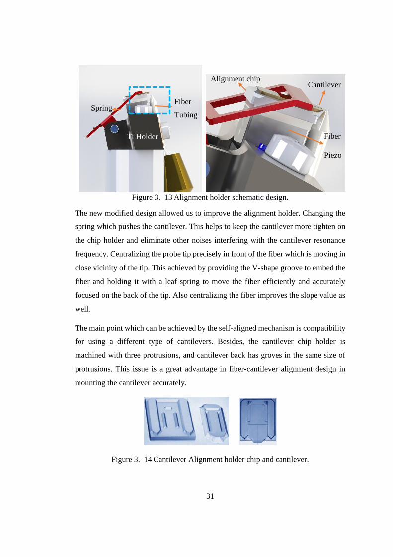
31
Figure 3. 13 Alignment holder schematic design.
The new modified design allowed us to improve the alignment holder. Changing the
spring which pushes the cantilever. This helps to keep the cantilever more tighten on
the chip holder and eliminate other noises interfering with the cantilever resonance
frequency. Centralizing the probe tip precisely in front of the fiber which is moving in
close vicinity of the tip. This achieved by providing the V-shape groove to embed the
fiber and holding it with a leaf spring to move the fiber efficiently and accurately
focused on the back of the tip. Also centralizing the fiber improves the slope value as
well.
The main point which can be achieved by the self-aligned mechanism is compatibility
for using a different type of cantilevers. Besides, the cantilever chip holder is
machined with three protrusions, and cantilever back has groves in the same size of
protrusions. This issue is a great advantage in fiber-cantilever alignment design in
mounting the cantilever accurately.
Figure 3. 14 Cantilever Alignment holder chip and cantilever.
Ti Holder
Spring
Cantilever Alignment chip
Fiber
Tubing
Fiber
Piezo

32
In the design, it is attempted to apply the similarly thermal contraction coefficient
material. (Table 3.3) The body which is manufactured of the Titanium is screwed on
the glued plastic holder (Polyphenylene sulfide (PPS)) on the top of the scanner piezo
tube. Technically the titanium part is assembled by the fiber piezo, cantilever
alignment chip, and the spring in the way that the fiber piezo sandwiched between two
small ceramic parts to avoid high voltage leaks and on the top of the ceramic the
cantilever alignment chip is positioned. All these parts are glued with a compatible
epoxy to the low-temperature. And the assembly is designed to stay in around 11
degrees tilted using a titanium holder that allows just the cantilever tip to get in contact
with the sample surface. In summary, the new alignment design is entirely reliable at
the low temperature, working range of 1-300 K without any collapse.
Figure 3. 15 Alignment holder of the cantilever in front of the fiber tubing
Table 3. 3 The dimensions and contraction coefficients α of the utilized material at
the design
Material Component α (10-6/K) Size Z (mm) Size XY/OD
(mm)
Alumina,
Al2O3
Ceramic 8 0.5 3 x 4
Lead
Zirconate
Titanium
Fiber piezo 6 2 3 x 3
Silicon, Cr
coated
Alignment chip 6 0.53 2.9 x 6.7
Titanium Alignment
holder
8.6 6 11 x 11
Silica, SiO2 Fiber 0.75 7 0.125
Zirconium Ferrule tubing 8 7 11
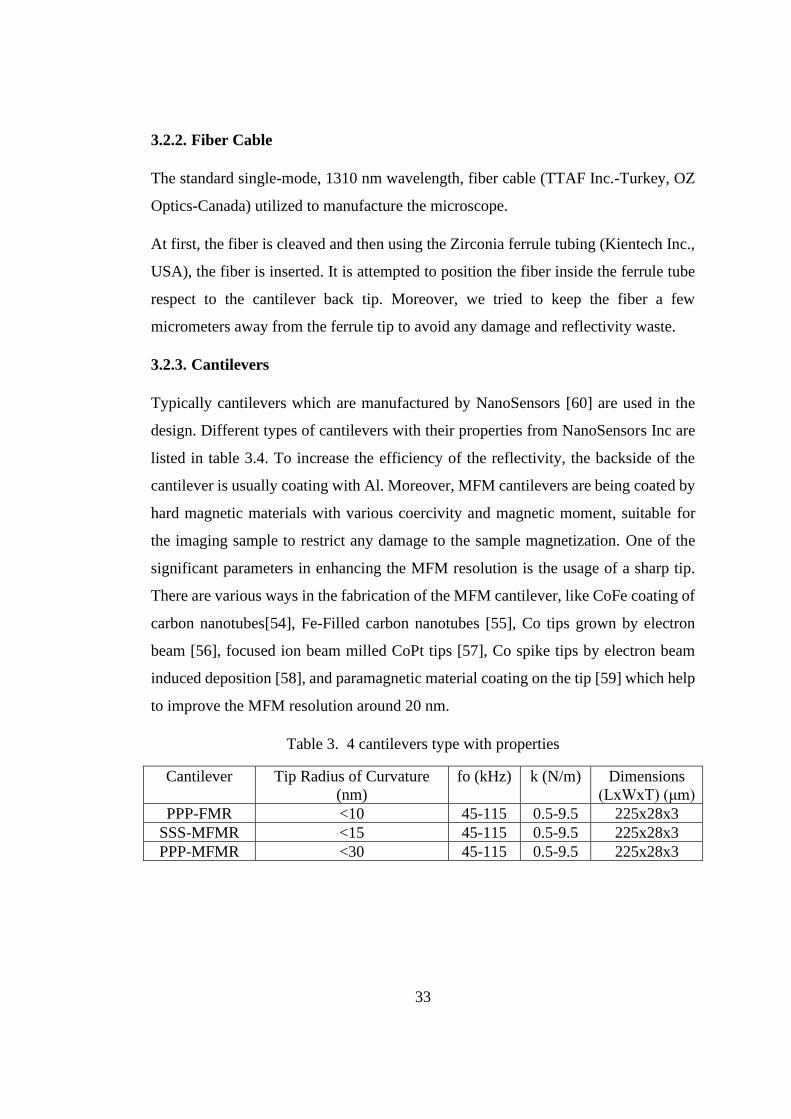
33
3.2.2. Fiber Cable
The standard single-mode, 1310 nm wavelength, fiber cable (TTAF Inc.-Turkey, OZ
Optics-Canada) utilized to manufacture the microscope.
At first, the fiber is cleaved and then using the Zirconia ferrule tubing (Kientech Inc.,
USA), the fiber is inserted. It is attempted to position the fiber inside the ferrule tube
respect to the cantilever back tip. Moreover, we tried to keep the fiber a few
micrometers away from the ferrule tip to avoid any damage and reflectivity waste.
3.2.3. Cantilevers
Typically cantilevers which are manufactured by NanoSensors [60] are used in the
design. Different types of cantilevers with their properties from NanoSensors Inc are
listed in table 3.4. To increase the efficiency of the reflectivity, the backside of the
cantilever is usually coating with Al. Moreover, MFM cantilevers are being coated by
hard magnetic materials with various coercivity and magnetic moment, suitable for
the imaging sample to restrict any damage to the sample magnetization. One of the
significant parameters in enhancing the MFM resolution is the usage of a sharp tip.
There are various ways in the fabrication of the MFM cantilever, like CoFe coating of
carbon nanotubes[54], Fe-Filled carbon nanotubes [55], Co tips grown by electron
beam [56], focused ion beam milled CoPt tips [57], Co spike tips by electron beam
induced deposition [58], and paramagnetic material coating on the tip [59] which help
to improve the MFM resolution around 20 nm.
Table 3. 4 cantilevers type with properties
Cantilever Tip Radius of Curvature
(nm)
fo (kHz) k (N/m) Dimensions
(LxWxT) (μm)
PPP-FMR <10 45-115 0.5-9.5 225x28x3
SSS-MFMR <15 45-115 0.5-9.5 225x28x3
PPP-MFMR <30 45-115 0.5-9.5 225x28x3
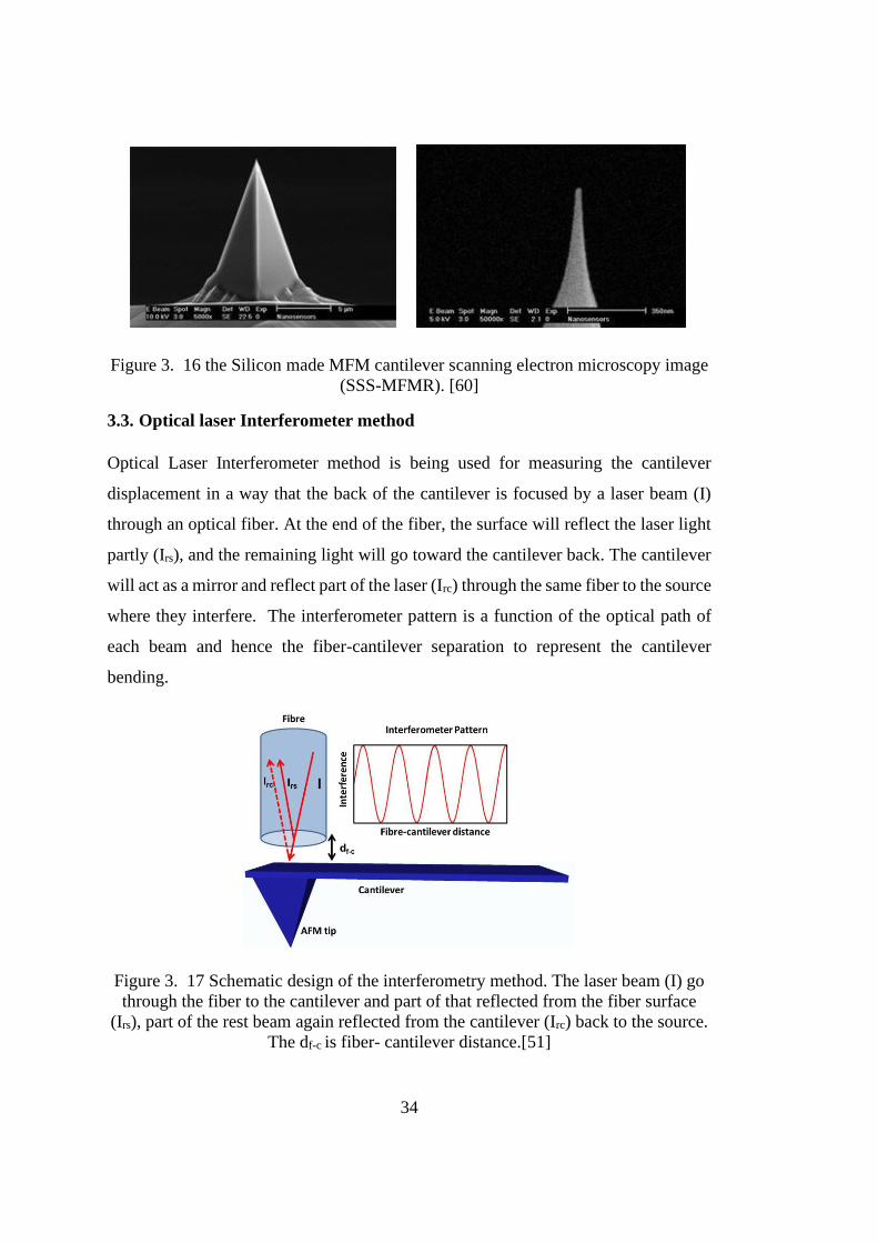
34
Figure 3. 16 the Silicon made MFM cantilever scanning electron microscopy image
(SSS-MFMR). [60] 3.3. Optical laser Interferometer method
Optical Laser Interferometer method is being used for measuring the cantilever
displacement in a way that the back of the cantilever is focused by a laser beam (I)
through an optical fiber. At the end of the fiber, the surface will reflect the laser light
partly (Irs), and the remaining light will go toward the cantilever back. The cantilever
will act as a mirror and reflect part of the laser (Irc) through the same fiber to the source
where they interfere. The interferometer pattern is a function of the optical path of
each beam and hence the fiber-cantilever separation to represent the cantilever
bending.
Figure 3. 17 Schematic design of the interferometry method. The laser beam (I) go
through the fiber to the cantilever and part of that reflected from the fiber surface
(Irs), part of the rest beam again reflected from the cantilever (Irc) back to the source.
The df-c is fiber- cantilever distance.[51]

35
3.3.1. Michelson Fiber Interferometer Principal and design
In order to measure the cantilever displacement, a low noise fiber interferometer with
the Michelson principal is designed, which is similar to Rugar design [37-38]. A 1310
nm laser diode with a constant power is coupled into 2x2 single-mode 50% fiber
splitter.
Figure 3. 18 Michelson fiber interferometer schematic design. [49]
After coupling the input laser, 50% goes through the fiber to the end of the cantilever
and reflected through the same cleaved fiber. The other 50% is connected to the
reference photodiode in order to monitor the laser power. Part of the reflection laser
is reflected from the end of the fiber (usually around 3%), and the rest light passes to
the cantilever. Both reflection light and light from reference photodiode is being
directed to the signal photodiode to interfere. The photocurrent generated by the
interference can be described as:
𝐼𝑖𝑛𝑡𝑒𝑟 = 𝐼0 [1 − 𝑉𝑐𝑜𝑠 (4𝜋𝑑𝑓−𝑐
𝜆)]
(3.3)
𝐼0 =𝐼𝑚𝑎𝑥 + 𝐼𝑚𝑖𝑛
2
(3.4)
𝑉 =𝐼𝑚𝑎𝑥 − 𝐼𝑚𝑖𝑛𝐼𝑚𝑎𝑥 + 𝐼𝑚𝑖𝑛
(3.5)
𝑅 =𝑉𝑠𝑖𝑔𝑛𝑎𝑙 − 𝑅𝐹−𝑠𝑖𝑔𝑛𝑎𝑙
𝑉𝑅𝑒𝑓𝑒𝑟𝑒𝑛𝑐𝑒 + 𝑅𝐹−𝑅𝑒𝑓𝑒𝑟𝑒𝑛𝑐𝑒
(3.6)

36
Where I0 is midpoint current, V is visibility, df-c the fiber-cantilever separation, R the
reflectivity, and 𝜆 the laser wavelength. The most sensitive positions in the
interferometer are the quadratures, d= 𝜆
8,3𝜆
8,5𝜆
8
Also, the slope of the interference can be calculated by:
𝑚 =∆𝐼
∆𝑑= 4𝜋𝐼0
𝑉
𝜆
(3.7)
Here respectively ∆𝑑 and m are the displacements of the cantilever and interference
pattern slope. The standard value for the interferometer interference slope is around 4
mV/Å. To maximize the precision of the measurement the equilibrium distance within
the cantilever and the fiber is arranged to be maximum of the interferometer slope
pattern. The max slope, which is the quadrature point on the interferometer could be
defined by mapping the pattern of the interference via displacing the cantilever with
the stack fiber piezo underneath it. The applied voltage to the fiber piezo in the two
directions of the forward and backward regard to the fiber is 0-100 V.
Figure 3. 19 Michelson Interferometer Interference pattern. The average slope is
4.27 mV/Å with visibility 0.27and at 327µWquadrature power.
3.3.2. LT-AFM controller

37
As already is explained, the interferometer measures the bending of the cantilever
which is received by Phase Lock Loop (PLL) card that is responsible to excite the
cantilever and the resonance frequency. Moreover, measuring the phase and amplitude
of the output signal from the cantilever.
A power supply system with very low noise is provided for the LT-AFM/MFM
controller which has a high voltage amplifier with four channels that drives the piezo.
An exponential pulse up to 400 V is generated to run the stick-slip mechanism from
the slider card.
The control mechanism description for LT-AFM/MFM microscope is presented in the
figure below.
Figure 3. 20 LT-AFM control scheme.[51]
Dash lines represent the connection between the microscope and different elements in
the controller. The interferometer records the information of the AFM probe
displacement and then transmits to the Phase Locked Loop card. Both the frequency
or amplitude shift is utilized for the feedback in the controller operation.

38
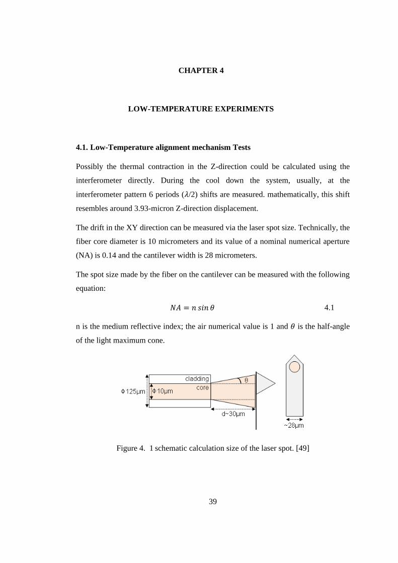
39
CHAPTER 4
4. LOW-TEMPERATURE EXPERIMENTS
4.1. Low-Temperature alignment mechanism Tests
Possibly the thermal contraction in the Z-direction could be calculated using the
interferometer directly. During the cool down the system, usually, at the
interferometer pattern 6 periods (𝜆/2) shifts are measured. mathematically, this shift
resembles around 3.93-micron Z-direction displacement.
The drift in the XY direction can be measured via the laser spot size. Technically, the
fiber core diameter is 10 micrometers and its value of a nominal numerical aperture
(NA) is 0.14 and the cantilever width is 28 micrometers.
The spot size made by the fiber on the cantilever can be measured with the following
equation:
𝑁𝐴 = 𝑛 𝑠𝑖𝑛 𝜃
4.1
n is the medium reflective index; the air numerical value is 1 and 𝜃 is the half-angle
of the light maximum cone.
Figure 4. 1 schematic calculation size of the laser spot. [49]
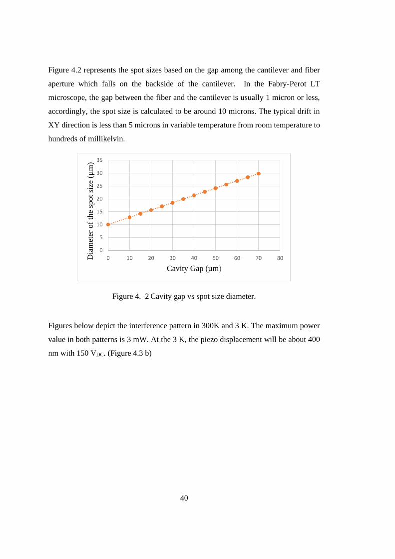
40
Figure 4.2 represents the spot sizes based on the gap among the cantilever and fiber
aperture which falls on the backside of the cantilever. In the Fabry-Perot LT
microscope, the gap between the fiber and the cantilever is usually 1 micron or less,
accordingly, the spot size is calculated to be around 10 microns. The typical drift in
XY direction is less than 5 microns in variable temperature from room temperature to
hundreds of millikelvin.
Figure 4. 2 Cavity gap vs spot size diameter.
Figures below depict the interference pattern in 300K and 3 K. The maximum power
value in both patterns is 3 mW. At the 3 K, the piezo displacement will be about 400
nm with 150 VDC. (Figure 4.3 b)
0
5
10
15
20
25
30
35
0 10 20 30 40 50 60 70 80Dia
met
er o
f th
e sp
ot
size
(µ
m)
Cavity Gap (µm)
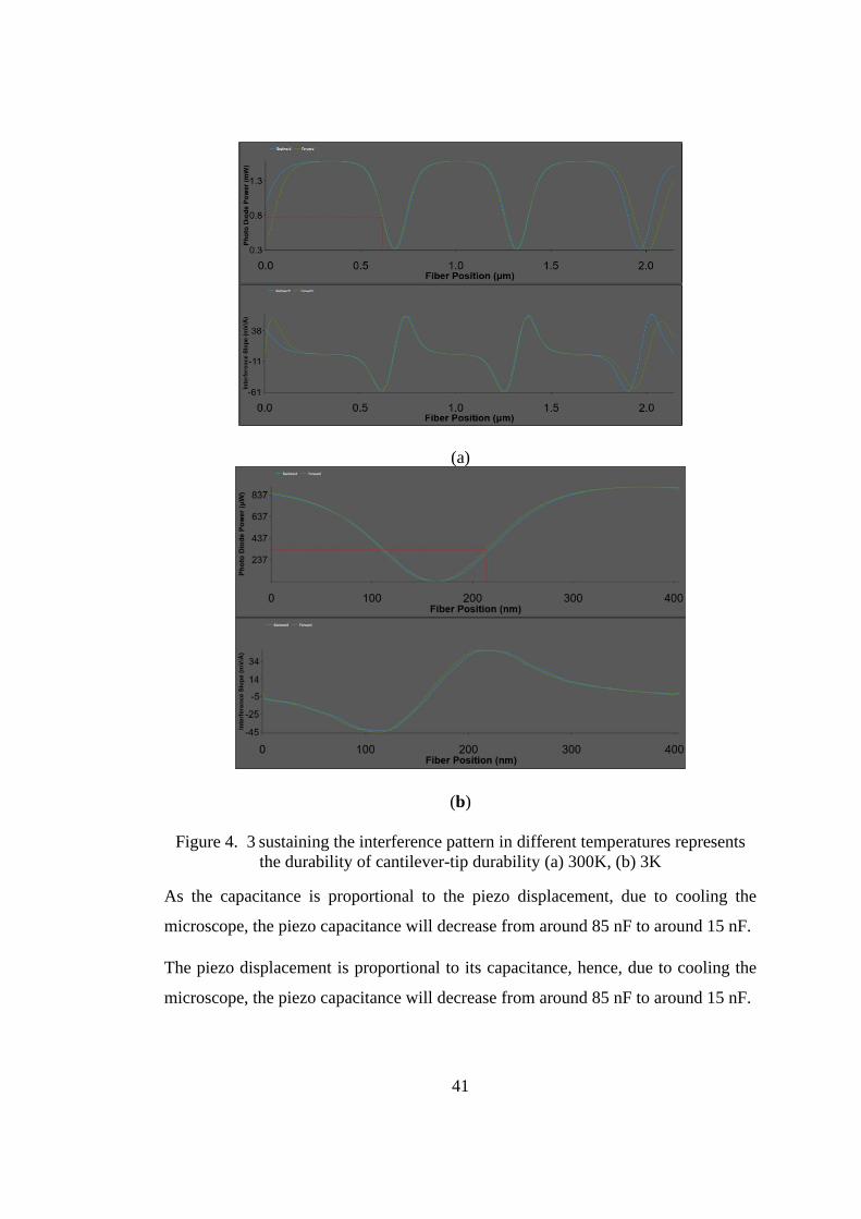
41
(a)
(b)
Figure 4. 3 sustaining the interference pattern in different temperatures represents
the durability of cantilever-tip durability (a) 300K, (b) 3K
As the capacitance is proportional to the piezo displacement, due to cooling the
microscope, the piezo capacitance will decrease from around 85 nF to around 15 nF.
The piezo displacement is proportional to its capacitance, hence, due to cooling the
microscope, the piezo capacitance will decrease from around 85 nF to around 15 nF.

42
Figure 4. 4 Fiber Piezo capacitance change at the different Temperatures.
4.2. Noise Analysis
There are three main categories of noises that are affecting the fiber interferometer
deflection sensor, namely, laser noise, shot noise, and electrical noise. The electrical
noise itself is divided to Johnson noise, voltage noise, and current noise.
Table 4. 1 Noise sources affecting the deflection sensor.
Total Noise
1. Shot Noise
2. Electrical
Noise
I. Johnson Noise
II. Voltage Noise
III. Current Noise
3. Laser Noise
4.2.1. Laser Noise
The random fluctuations of various output parameters are summarized in a short term
of Noise in the laser. This is a frequently encountered aspect that has an intense
influence on various applications in photonics, especially in the area of accurate
measurements. Consider e.g. variations of the transmission spectroscopic
measurements or optical phase can affect interferometric position measurements,
0
10
20
30
40
50
60
70
80
90
0 50 100 150 200 250 300 350
C (
nF)
T (K)
43
where fluctuations of intensity restrict the feasible sensitivity. Furthermore, noise
issues at least partially limit the data rate and the transmission distance for fiber-optic
links.
Based on the different impact of the quantum noise and fluctuation of the several
technical origins, the output of a laser noise constantly includes some noise. In a
single-frequency laser, there are intensity or amplitude noise and phase noise.
The origins of the laser noise can be classified in quantum noise, in particular,
correlated with the spontaneous emission in the gain medium and technical noise such
as the excess noise if the pump source, or vibration of the resonator, or from
temperature changes.
Moreover, the laser intensity is affected by many intrinsic noise sources of the laser
diodes. The laser intensity noise can be described as:
𝜈2̅̅ ̅𝑖𝑛𝑡𝑒𝑛𝑠𝑖𝑡𝑦 = 𝑆𝑃𝐷2 𝑃2𝑅𝐹
2 × 10⁻¹³ (𝑉2
𝐻𝑧)
4.2
Here SPD is the photodetector responsibility, P is the optical power of the incident
beam, and RF is, the feedback resistor to the photodetector I-V converter.
The laser phase noise also depends on the cavity gap between the cantilever and fiber.
The laser noise can be defined as :
𝜈2̅̅ ̅𝑝ℎ𝑎𝑠𝑒 = 𝑆𝑃𝐷2 𝑃2𝑅𝐹
24𝜋∆𝜈 𝜏2 × 10⁻¹³ (𝑉2
𝐻𝑧)
4.3
The 𝜏 is the length difference of the optical path in the cavity gap which is divided by
the light speed, and ∆𝜈 is the laser diode bandwidth.
4.2.2. Shot Noise
Poisson or Shot noise is a sort of noise that could be determined with a Poisson
process. The shot noise arises from the discrete feature of the electric charge. The
electronic current random fluctuations are the origination of the shot noise in the DC
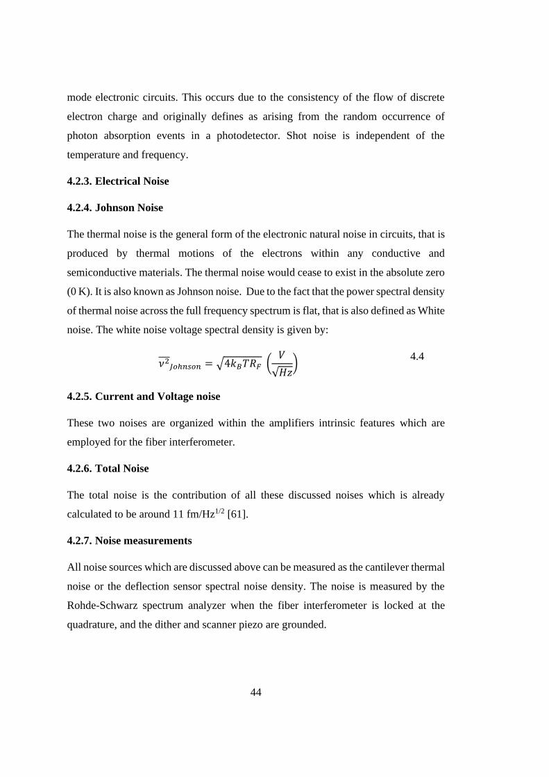
44
mode electronic circuits. This occurs due to the consistency of the flow of discrete
electron charge and originally defines as arising from the random occurrence of
photon absorption events in a photodetector. Shot noise is independent of the
temperature and frequency.
4.2.3. Electrical Noise
4.2.4. Johnson Noise
The thermal noise is the general form of the electronic natural noise in circuits, that is
produced by thermal motions of the electrons within any conductive and
semiconductive materials. The thermal noise would cease to exist in the absolute zero
(0 K). It is also known as Johnson noise. Due to the fact that the power spectral density
of thermal noise across the full frequency spectrum is flat, that is also defined as White
noise. The white noise voltage spectral density is given by:
𝜈2̅̅ ̅𝐽𝑜ℎ𝑛𝑠𝑜𝑛 = √4𝑘𝐵𝑇𝑅𝐹 (𝑉
√𝐻𝑧)
4.4
4.2.5. Current and Voltage noise
These two noises are organized within the amplifiers intrinsic features which are
employed for the fiber interferometer.
4.2.6. Total Noise
The total noise is the contribution of all these discussed noises which is already
calculated to be around 11 fm/Hz1/2 [61].
4.2.7. Noise measurements
All noise sources which are discussed above can be measured as the cantilever thermal
noise or the deflection sensor spectral noise density. The noise is measured by the
Rohde-Schwarz spectrum analyzer when the fiber interferometer is locked at the
quadrature, and the dither and scanner piezo are grounded.

45
The spectral noise density can be calculated mathematically and fitted to the
experimental data [62]:
𝑆 =√
2𝑘𝐵𝑇
𝜋𝑓0𝑘𝑄
1
(1 − (𝑓𝑓0)2
)
2
− (𝑓𝑓0𝑄)
2
4.5
Where f0, f, T, Q, k and KB respectively are resonance frequency, frequency,
temperature, Q-factor, cantilever spring constant, and Boltzmann constant.
The experiment was done in 300 K with the normal tapping, non-contact mode
cantilever from NanoSensors Inc (PPP-NCLR) which has a spring constant of 21-98
N/m. Mathematically, the cantilever spring constant is calculated to be 70 N/m using
the thermal noise spectrum.
Figure 4. 5 The fiber interferometer spectrum noise density at 300 K.
Also, the graph is fitted by the theoretical calculation with f0 168 kHz, Q factor 500,
k is 70 N/m.
The laser power also has an effect on the deflection sensor. Decreasing laser power
makes extreme noise. The main reason for this dramatic noise is shot noise.
1.0
2.0
4.0
8.0
16.0
32.0
64.0
128.0
256.0
512.0
140 150 160 170 180 190
Nois
e (f
m/√
Hz)
Frequency (kHz)
Ultra Low Noise Fabry-Perot Interferometer
FP Noise (fm/√Hz) Calculated Brownian Noise (fm/√Hz)
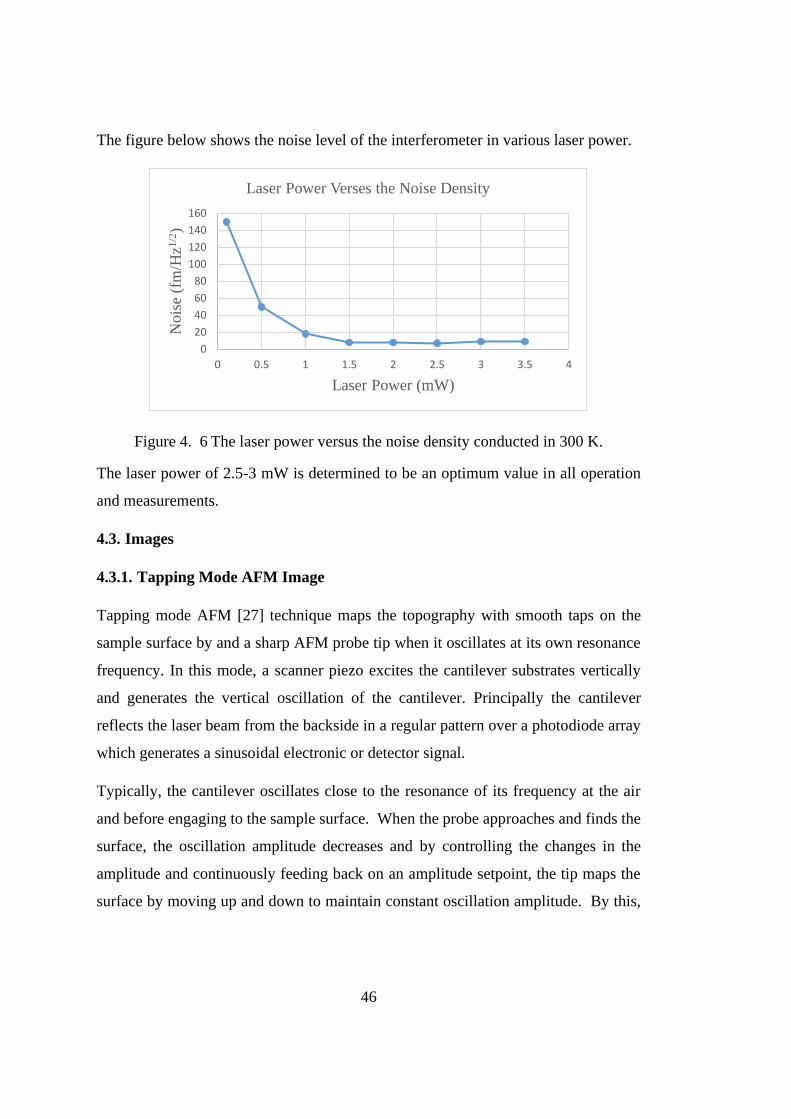
46
The figure below shows the noise level of the interferometer in various laser power.
Figure 4. 6 The laser power versus the noise density conducted in 300 K.
The laser power of 2.5-3 mW is determined to be an optimum value in all operation
and measurements.
4.3. Images
4.3.1. Tapping Mode AFM Image
Tapping mode AFM [27] technique maps the topography with smooth taps on the
sample surface by and a sharp AFM probe tip when it oscillates at its own resonance
frequency. In this mode, a scanner piezo excites the cantilever substrates vertically
and generates the vertical oscillation of the cantilever. Principally the cantilever
reflects the laser beam from the backside in a regular pattern over a photodiode array
which generates a sinusoidal electronic or detector signal.
Typically, the cantilever oscillates close to the resonance of its frequency at the air
and before engaging to the sample surface. When the probe approaches and finds the
surface, the oscillation amplitude decreases and by controlling the changes in the
amplitude and continuously feeding back on an amplitude setpoint, the tip maps the
surface by moving up and down to maintain constant oscillation amplitude. By this,
0
20
40
60
80
100
120
140
160
0 0.5 1 1.5 2 2.5 3 3.5 4
Nois
e (f
m/H
z1/2
)
Laser Power (mW)
Laser Power Verses the Noise Density

47
we can reach the high-resolution three-dimensional image of the sample surface
topography.
1. Cantilever oscillates in free air.
Amplitude is larger than the set point.
2. Tapping on the sample. Cantilever
oscillates at setpoint amplitude.
3. Tip encounters a particle. Cantilever
oscillation amplitude drops
4. The piezo lifts due to the feedback to
returns the Amplitude to the setpoint.
Figure 4. 7 cantilever motion in tapping mode. [63]
The tapping mode technique is one of the important methods in scanning probe
microscopy as it overcomes some of the restrictions in contact mode AFM by
eliminating the lateral forces to the surface which can distort or damage the sample.
The capability of working in both air and the fluid environment as well as routine
imaging of the soft and delicate samples, or samples which are weekly attached to a
substrate which are difficult to be operated in contact mode AFM are the vital features
of tapping mode AFM.

48
When the drive frequency is at or close to the resonance frequency of the cantilever,
the shacking of the piezo can provide a large cantilever oscillation around 2-100 nm
in free air. Though, drive frequency away from the cantilever resonance frequency
results in the amplitude drop immediately. This is because the cantilever's natural
response is out of phase and the piezo shaking energy is less efficiently transfer to the
cantilever. Therefore, driving the cantilever at its resonance frequency results in the
constant oscillation amplitude. And when the cantilever is brought close to the surface
the force gradient between the tip and the sample effects to the resonant frequency and
potentially makes the shift and the amplitude of the oscillation reduces. The attractive
forces make the resonance frequency shift get lower, and repulsive forces, make the
frequency shift higher.
Figure 4. 8 Cantilever oscillation amplitude vs. drive frequency. [63]
Additionally, to the topography image, the phase image can be recorded by the tapping
mode. The phase image provides data about the material hardness, both charge or
magnetic field distribution within precise measurements and composition. Also, the
tapping mode is utilized for MFM measurements in the way that forward scans with
the same principal present the topography image and the backward scans give the
phase shift as well as magnetic image.
Figure 4.9 shows the atomic steps of the Mika layers imaged with the tapping mode
technique. For the sample preparation, firstly the Mika is cleaved by scotch tape and
etched with a 49% HF solution for 4 hours. Then washed with the deionized water and
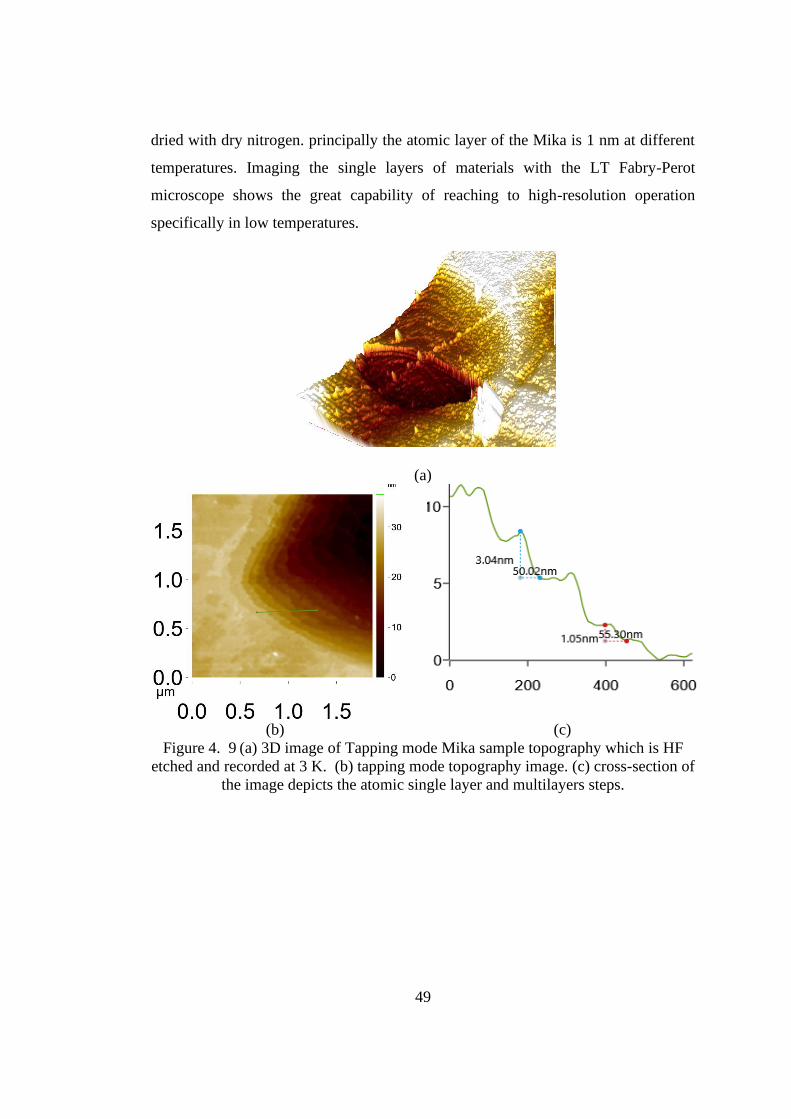
49
dried with dry nitrogen. principally the atomic layer of the Mika is 1 nm at different
temperatures. Imaging the single layers of materials with the LT Fabry-Perot
microscope shows the great capability of reaching to high-resolution operation
specifically in low temperatures.
(a)
(b) (c)
Figure 4. 9 (a) 3D image of Tapping mode Mika sample topography which is HF
etched and recorded at 3 K. (b) tapping mode topography image. (c) cross-section of
the image depicts the atomic single layer and multilayers steps.
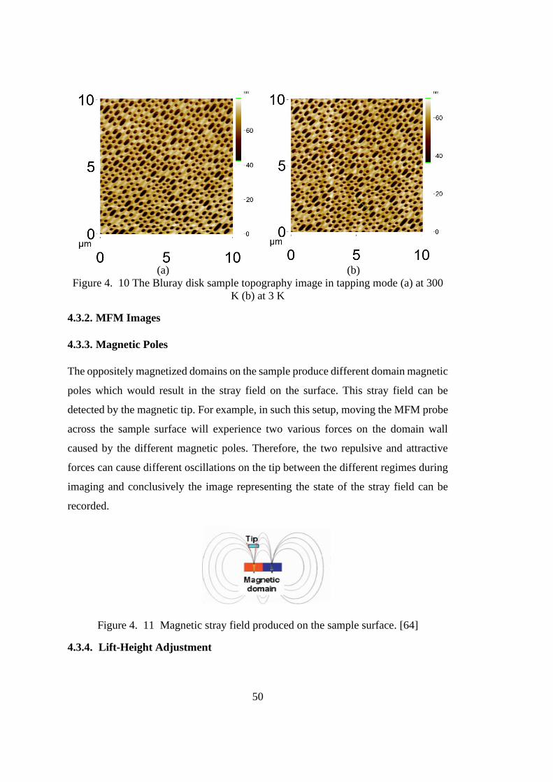
50
(a) (b)
Figure 4. 10 The Bluray disk sample topography image in tapping mode (a) at 300
K (b) at 3 K
4.3.2. MFM Images
4.3.3. Magnetic Poles
The oppositely magnetized domains on the sample produce different domain magnetic
poles which would result in the stray field on the surface. This stray field can be
detected by the magnetic tip. For example, in such this setup, moving the MFM probe
across the sample surface will experience two various forces on the domain wall
caused by the different magnetic poles. Therefore, the two repulsive and attractive
forces can cause different oscillations on the tip between the different regimes during
imaging and conclusively the image representing the state of the stray field can be
recorded.
Figure 4. 11 Magnetic stray field produced on the sample surface. [64]
4.3.4. Lift-Height Adjustment

51
The other force sources like Van der Wall forces aside from the magnetic force
influence on the tip, therefore it is necessary that the probe kept in a specific distance
through imaging. Here the importance of the two-pass technique is obvious, recording
the topography image in forwarding and magnetic image in backward in specific lift
height. The lift-amount is so critical to image an ideal magnetic image. This provides
the chance to keep the tip in a specific height to interact with magnetic stray field
better and away from other interactions. In case the lift amount is not sufficient, the
magnetic image can be contained with the topographic features as the tip still under
the effects of the short-range forces.
(a) (b)
(c) (d)
Figure 4. 12 Sony hi8 tape MFM images with different lift height parameters. (a) 80
nm, (b) 100 nm, (c) 120nm, (d) 150 nm
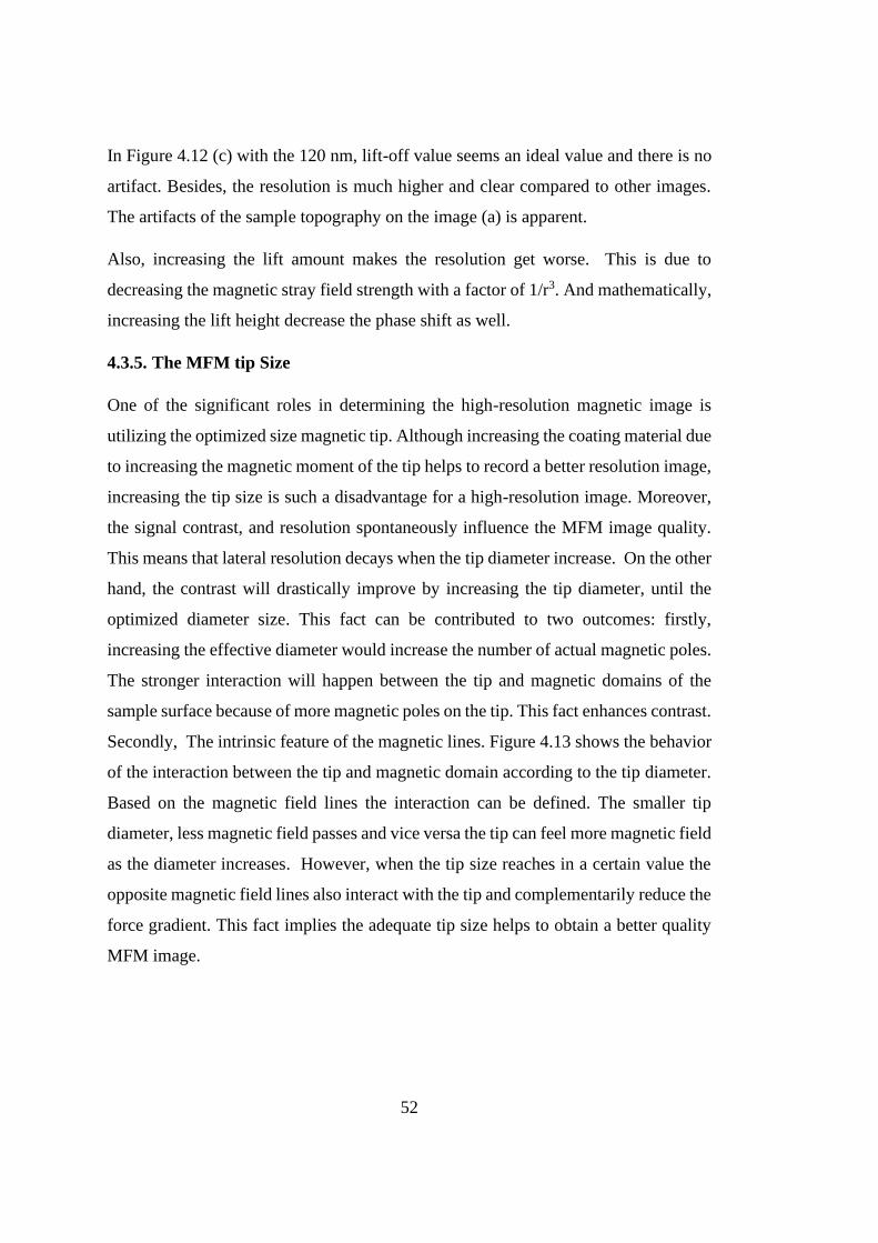
52
In Figure 4.12 (c) with the 120 nm, lift-off value seems an ideal value and there is no
artifact. Besides, the resolution is much higher and clear compared to other images.
The artifacts of the sample topography on the image (a) is apparent.
Also, increasing the lift amount makes the resolution get worse. This is due to
decreasing the magnetic stray field strength with a factor of 1/r3. And mathematically,
increasing the lift height decrease the phase shift as well.
4.3.5. The MFM tip Size
One of the significant roles in determining the high-resolution magnetic image is
utilizing the optimized size magnetic tip. Although increasing the coating material due
to increasing the magnetic moment of the tip helps to record a better resolution image,
increasing the tip size is such a disadvantage for a high-resolution image. Moreover,
the signal contrast, and resolution spontaneously influence the MFM image quality.
This means that lateral resolution decays when the tip diameter increase. On the other
hand, the contrast will drastically improve by increasing the tip diameter, until the
optimized diameter size. This fact can be contributed to two outcomes: firstly,
increasing the effective diameter would increase the number of actual magnetic poles.
The stronger interaction will happen between the tip and magnetic domains of the
sample surface because of more magnetic poles on the tip. This fact enhances contrast.
Secondly, The intrinsic feature of the magnetic lines. Figure 4.13 shows the behavior
of the interaction between the tip and magnetic domain according to the tip diameter.
Based on the magnetic field lines the interaction can be defined. The smaller tip
diameter, less magnetic field passes and vice versa the tip can feel more magnetic field
as the diameter increases. However, when the tip size reaches in a certain value the
opposite magnetic field lines also interact with the tip and complementarily reduce the
force gradient. This fact implies the adequate tip size helps to obtain a better quality
MFM image.
53
Figure 4. 13 Tip interaction in the magnetic field domain.[64]


55
CHAPTER 5
5. LOW TEMPERATURE
5.1. The Cryogenic temperature
The definition of the cryogenic temperature starts from -150 ºC to the absolute zero -
273 ºC, which is the temperature that molecular movement becomes close to the
theoretically possible to completely stop.
Principally, the cryogenic temperatures happen below the temperatures which are
faced in the common physical processes. In that severe circumstances, the features of
the materials such as ductility, strength, thermal conductivity, and the electric
resistance are changed in both theoretical and commercial importance, as the heat is
generated by the random movement of the molecules. Materials in the extremely low
temperature are highly ordered and close to the static state.
In 1877, after cooling the oxygen to its liquid point for the first time (90 K), the
cryogenics had begun. Then the theoretical development due to the development of
the refrigeration systems started. In 1895, it was the possibility to reach to 40 K and
liquified the air and separate into the main components. The helium liquified at 4.2 K,
in 1908, and then after the attempt to supercooled materials and lose the resistance to
electricity led to discover the superconductivity phenomenon. The absolute zero was
reached in the 1920s and 1930s. And since 1960, laboratories are capable to
experiment a millikelvin temperature.
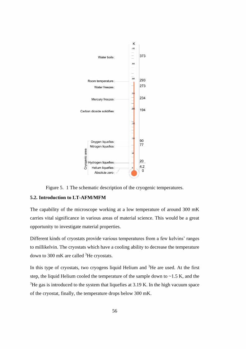
56
Figure 5. 1 The schematic description of the cryogenic temperatures.
5.2. Introduction to LT-AFM/MFM
The capability of the microscope working at a low temperature of around 300 mK
carries vital significance in various areas of material science. This would be a great
opportunity to investigate material properties.
Different kinds of cryostats provide various temperatures from a few kelvins’ ranges
to millikelvin. The cryostats which have a cooling ability to decrease the temperature
down to 300 mK are called 3He cryostats.
In this type of cryostats, two cryogens liquid Helium and 3He are used. At the first
step, the liquid Helium cooled the temperature of the sample down to ~1.5 K, and the
3He gas is introduced to the system that liquefies at 3.19 K. In the high vacuum space
of the cryostat, finally, the temperature drops below 300 mK.

57
5.2.1. Dry Cryostat
A cryogen-free design is meaning that no liquid cryogens are required to cool the
system or during normal operation. The cooling system consists of a cold head
mounted on the cryostat and an external compressor. The cold head cools both the
magnet and radiation shields within the cryostat as well as the recirculating helium
gas in the gas handling system (GHS). Respectively the radiation shield and magnet
can arrive at their base temperatures of 40 K and 3.5 K.
The system uses helium gas in the gas handling system (GHS) to cool the variable
temperature insert (VTI) as an exchange gas inside the sample space. Because of this,
both the GHS and the sample space must be filled with helium gas before the system
is cooled.
Without the gas recirculating, the VTI and sample will cool to about 150 K when the
system reaches its base temperature. In the GHS, the helium gas is pumped into the
cryostat connection lines and cooled as it passes through a series of heat exchangers
attached to the cryocooler, before passing through a needle valve in the VTI. As the
helium gas exits the needle valve, it expands and cools via the Joule-Thompson
principal, and enabling the VTI to reach temperatures below 1.8 K. The expanded gas
is then pumped back out of the cryostat and reinjected in a continuous cycle.
v
The sample itself sits in a helium exchange gas which is not part of the circulation
loop. This greatly reduces any chance of contamination of the recirculation loop gas
when changing samples.
The procedure can be operated by balancing the cooling and heating power,
respectively with recirculating helium to cool and heaters, as a pair of cartridge heaters
positioned on the tail of the VTI. The sample heater controls the sample temperature
under normal conditions from 1.3 K to 300 K. Therefore, the cryostat provides the
capability for all ranges of temperature for different experiments.

58
Figure 5. 2 The cryostat and gas handling system schematic design. [65]
5.3. Cryocoolers
A refrigeration machine which is the main part of the cryostats with the capability of
cooling lower than123 K and a small refrigeration space is called the cryocooler.
Principally, recuperative and regenerative are two types of cryocoolers. The former
includes the Brayton and Joules Thomson type, and the latter involves Stirling and
Gifford-McMahon type cryocooler. Mainly cryocoolers are utilized to cool the
infrared sensors in the missile guided system and satellite-based surveillance, the
cooling of superconductors and semiconductors, as well as applications such as in
cryopumps, liquefying natural gases, cooling of radiation shields, SQUID
(superconducting quantum interference device), Magnetometers, Semiconductor
fabrication, etc.

59
Explicitly the high usage demand for cryocoolers, small size, long lifetime,
performance efficiency, reliability, low vibration, and weight become important
aspects in the development of cryocoolers. The smaller heat transfer loss and higher
efficiency of the Stirling and Gifford-McMahon (G-M) type cryocoolers bring them
to a widely used in many applications. Due to the construction simplicity by
eliminating the moving part at the cold end, pulse tube cryocoolers have more
advantages over other cryocoolers and reliable in operation. Generally, there are two
types of pulse tube cryocoolers. The table below represents the overall comparison of
these two systems.
Table 5. 1 Stirling and G-M type Cryocoolers Comparison.
G-M type cryocooler Stirling type cryocooler
Use of oil-lubricated compressor Use of dry compressor
Working at Low frequency (1-5Hz) Working at high frequency (20-120Hz)
A compressor connected to the expander
through a valve
Compressor directly connected to the
expander
Pressure ratios are high Pressure ratios are low
Low Coefficient of performance High Coefficient of performance
Compressors are bulky (capacity is in
kW)
Compressors are small (capacity is in
few hundreds Watts)
Can a below 2K using two stages of
cooler
Can attain 20K using two stages of
cooler

60
Pulse Tube cryocoolers or Refrigerators are pulsing the pressure from one end of a
hollow tube and observing cooling effect from the other end for the first time is
recognized by Gifford and Longsworth in the early sixties. This was the initiation of
the most promising cryogenics refrigerators Comparison which is classified as basic
pulse tube refrigerators (BPTR). This type of refrigerators is more in the attention
because of enhanced reliability, long lifetime, and simplicity because of the absence
in the moving part at the cold temperature region.
The pulse tube refrigerators (PTR), unlike the other typical refrigerators which are
using the vapor compression cycle based on the classical thermodynamics, is achieved
by the oscillatory compression theory and gas expansion within the enclosed volume
to reach the desired refrigeration. Based on being oscillatory, a PTR is not a steady
system that demands the time-dependent solution. However, PTRs are a quasi-steady
periodic state (steady-periodic mode). Principally, a periodic steady system is a cycle
that will reach the same state in the next cycle and so on. The PTRs are working in a
closed system with using the oscillation pressure which is regularly provided by an
oscillatory piston in one end to generate a flow of oscillating gas in the rest of the
system. Here the gas is responsible to carry the heat away from the point with low
temperature (cold heat exchanger) to the hot end exchanger.
Figure 5. 3 (a) Stirling (b) G-M type BTR Schematics. 1.Compressor, 2.
Aftercooler, 3. Regenerator, 4. Cold heat exchanger, 5. Pulse tube, 6. Hot heat
exchanger, 7. Valve [66]
61
The heat of compressor compression in a Stirling type PTR is removed by the
environment with a heat exchanger which is placed between the regenerator and
compressor. The heat exchanger is known as an aftercooler or precooler. These
principles are used in PTRs, present a capability to reach a temperature around 50 K.
Although the Stirling type can produce higher cooling power due to the absence of the
valve, the required rapid flow oscillation of the fluid heat exchange in this type limits
the performance at the low temperatures, such 10 K and below.
The G-M type PTR by utilizing the valve, it can dispense low/high-pressure gas into
the pulse tube. In this type of system, pulsation pressure is produced by the periodic
opening/closing operation of the high/low-pressure valve.
The main components of the PTR are Compressor, aftercooler, regenerator, cold heat
exchanger, pulse tube, and warm heat exchanger. Respectively each part are
responsible for supplying the pressurized and depressurized gas to the closed chamber,
ideally to extract all the heat which is produced in the compressor volume during the
gas compression and release to the environment, as the most important component in
the pulse tube refrigerators which is functionalized to absorb the heat during the
forward stroke from the incoming gas and return that heat back to the gas in return
stroke, the best resemblance to the evaporator in the vapor compression refrigeration
cycle where the system absorbs the refrigeration load, to carrying the heat with
enthalpy flow from the cold end to the warm end, and rejecting the generated heat
from the gas.
The most recent invention is the inertance tube PTR. In the aforementioned type, the
orifice valve is replaced by a long inertance tube which has a very small inner diameter
and adds reactive impedance to the system. This modification generates a phase shift
inside the pule tube and provides an enhanced enthalpy flow.
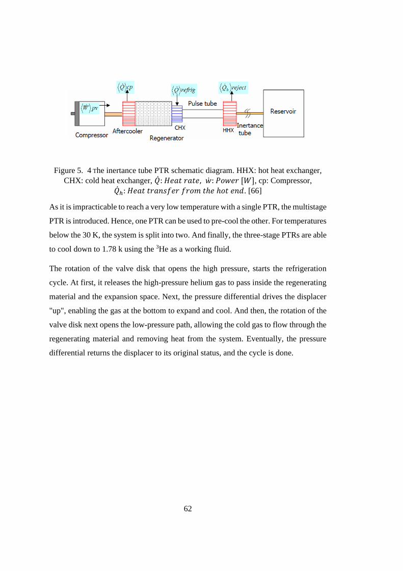
62
Figure 5. 4 The inertance tube PTR schematic diagram. HHX: hot heat exchanger,
CHX: cold heat exchanger, �̇�: 𝐻𝑒𝑎𝑡 𝑟𝑎𝑡𝑒, �̇�: 𝑃𝑜𝑤𝑒𝑟 [𝑊], cp: Compressor,
�̇�ℎ: 𝐻𝑒𝑎𝑡 𝑡𝑟𝑎𝑛𝑠𝑓𝑒𝑟 𝑓𝑟𝑜𝑚 𝑡ℎ𝑒 ℎ𝑜𝑡 𝑒𝑛𝑑. [66]
As it is impracticable to reach a very low temperature with a single PTR, the multistage
PTR is introduced. Hence, one PTR can be used to pre-cool the other. For temperatures
below the 30 K, the system is split into two. And finally, the three-stage PTRs are able
to cool down to 1.78 k using the 3He as a working fluid.
The rotation of the valve disk that opens the high pressure, starts the refrigeration
cycle. At first, it releases the high-pressure helium gas to pass inside the regenerating
material and the expansion space. Next, the pressure differential drives the displacer
"up", enabling the gas at the bottom to expand and cool. And then, the rotation of the
valve disk next opens the low-pressure path, allowing the cold gas to flow through the
regenerating material and removing heat from the system. Eventually, the pressure
differential returns the displacer to its original status, and the cycle is done.

63
Figure 5. 5 The schematic of the cryocooler working principal. [67]
The cryostat system in all these experiments is the top-loading (TL) C-Mag from
Cryomagnetics Instruments Inc. consists of a cold head mounted on the cryostat and
an external compressor. The cold head has the capability of reaching 1.3 K. And the
superconducting magnetic can provide 9 Tesla magnetic field which is integrated
inside the cryostat.
Figure 5. 6 (a) The cryostat, and (b) Isolation Vibration Platform.
(a)
(b)

64
5.4. Vibration Isolation
There are various factors coming from the environment which affects drastically the
scanning probe microscopy (SPM) measurements. Technically, based on different
environments in which the device has housed, these effects play a critical role. The
vibration noise is the main issue that AFM measurements are highly susceptible to
interference with. The two foremost types of vibration sense by AFM are mechanical
and acoustic vibrations. Almost the acoustic nose could be eliminated by locating the
instrument in an ideal place, far from the crowded place and audible activities as well
as providing a sealed cabinet covered with soundproof material or damping one.
Transmission mechanical vibration to the AFM stage is more important as there are
more sources of this strong type of vibration. Hence, all vibration sources in the
laboratory should be considered particularly. For instance, the laboratory floor noises
coming from the place that dry cryostat parts are positioned like cryocooler, pumping
and connection lines, chiller, and etc.
The dry cryostats that are more common in scientific sections have affordable prices,
easy to use, and elimination of He expense which is such advantages. The central
drawback of this system is the vibration generated by the pulse tube transferring
straight to the microscope. Here, the isolation vibration stage which specially designed
for the cryostat can solve the mechanical noise problem by decoupling the pulse tube
vibration. (Figure 5.6) In this design, the microscope is positioned on the vibration
isolation stainless steel platform with around 300 Kg which is held on three air
damping isolation legs [68].

65
Figure 5. 7 The vibration isolation table schematic design. (a), (b), and (c) are air
damping isolation legs, (d) is an edge welded bellows, (e) platform.
The vibration table is connected with a cylindrical spring-type extension part to adsorb
and separate the cryostat vibration from the microscope stage. Manufacturing the
design with nonmagnetic material helps for high field application researches.
Additionally, the compressor line connections are passed through a tighten concrete
hole to decrease the noise coming from the circulation of the Helium gas.
Moreover, to diminish the noise pathing through the electronic connection cables,
directly to the microscope, a heavy block of the 50 Kg is manufactured in the way that
cables can sandwich in between two heavy block parts and then tighten with screws.
(a)
(b) (c)
(d)
(e)
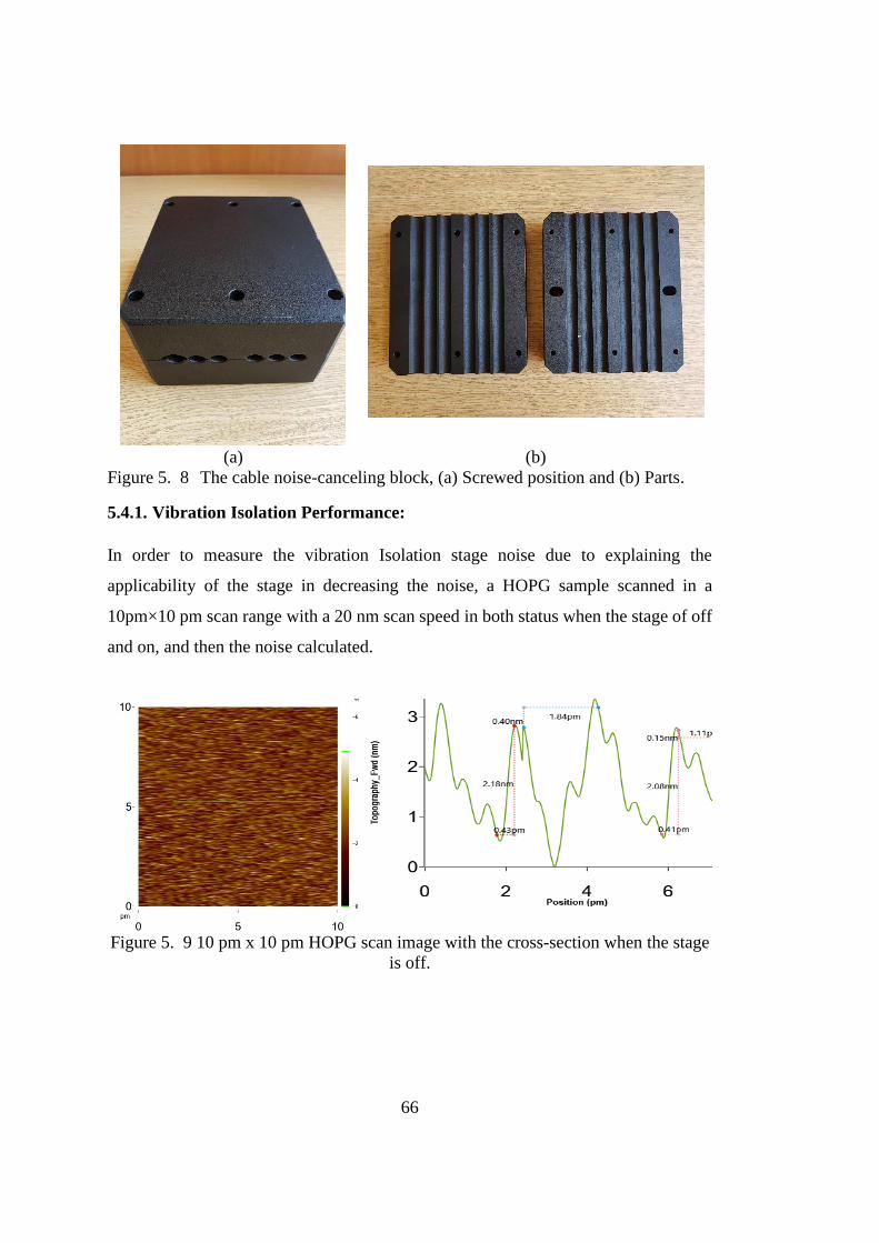
66
(a) (b)
Figure 5. 8 The cable noise-canceling block, (a) Screwed position and (b) Parts.
5.4.1. Vibration Isolation Performance:
In order to measure the vibration Isolation stage noise due to explaining the
applicability of the stage in decreasing the noise, a HOPG sample scanned in a
10pm×10 pm scan range with a 20 nm scan speed in both status when the stage of off
and on, and then the noise calculated.
Figure 5. 9 10 pm x 10 pm HOPG scan image with the cross-section when the stage
is off.
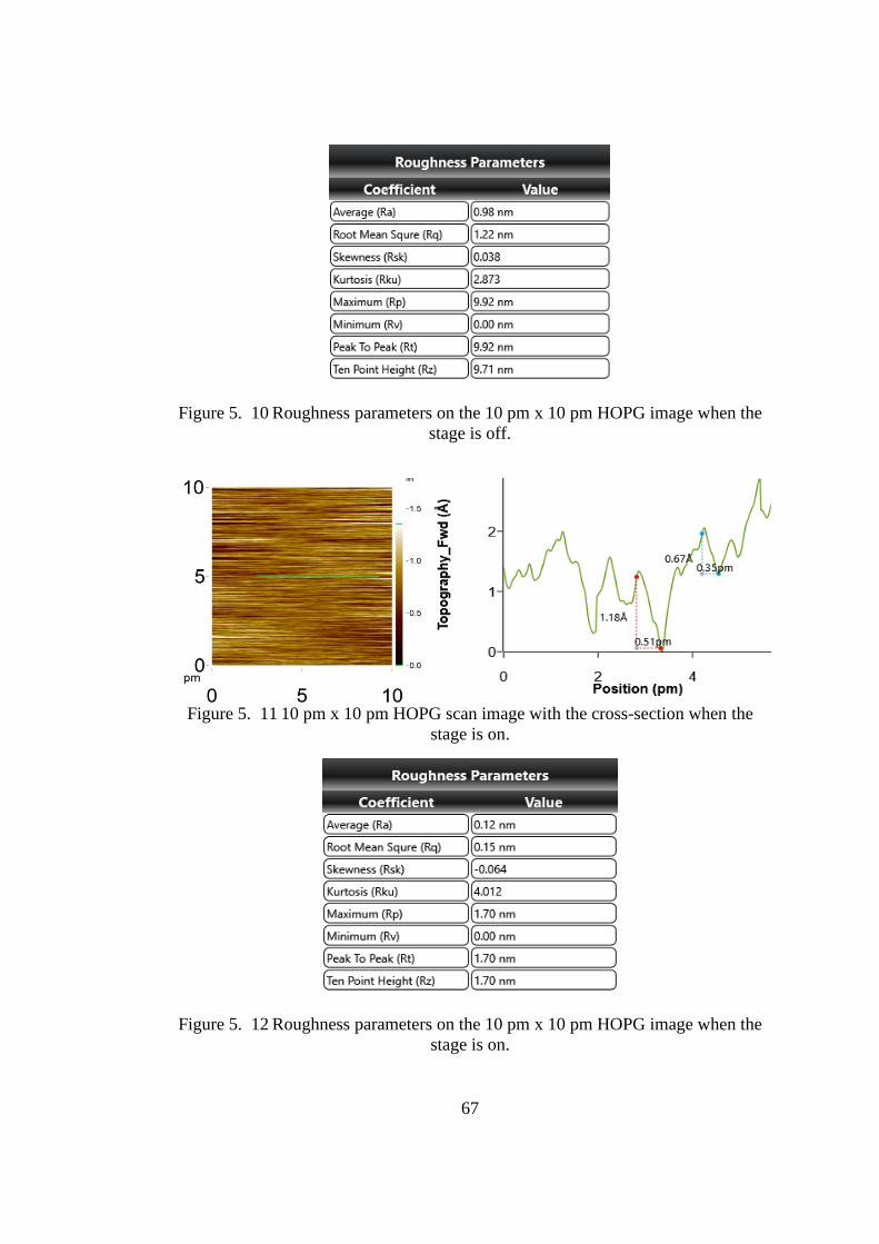
67
Figure 5. 10 Roughness parameters on the 10 pm x 10 pm HOPG image when the
stage is off.
Figure 5. 11 10 pm x 10 pm HOPG scan image with the cross-section when the
stage is on.
Figure 5. 12 Roughness parameters on the 10 pm x 10 pm HOPG image when the
stage is on.

68
The obtained the RMS noise in the existence of all noise around without utilizing the
isolation platform was 1.2 nm while performing the isolation stage the noise level is
reduced to 0.16 nm. This is suitable for most of the MFM applications using force
microscopy as well as the atomic resolution imaging or manipulation. Furthermore,
the histogram FWHM analysis claims the same level of the noise in both situations.
(a)
(a)
Figure 5. 13 histogram FWHM analysis of the scanned 10 pm x10pm HOPG (a)
Vibration isolation platform is off, (b) Vibration Isolation platform is on.
5.5. Images
In order to examine the functionality of the microscope inside at the cold temperature,
an iPhone camera chip was imaged by the AFM tapping mode in different
0
500
1000
1500
2000
2500
0 200 400 600
Nu
mb
er o
f P
ixel
s
nm
1.543 nm
0
100
200
300
400
500
600
700
800
0 100 200 300
Nu
mb
er o
f P
ixel
s
Å
1.30 Å

69
temperatures. Furthermore, the applicability of the vibration isolation platform is
monitored by imaging the single layers of the graphene (0.34 nm).
(a) (b)
(c)
Figure 5. 14 AFM topography images of the iPhone camera chip in Tapping mode,
(a) 225 K, (b) 77 K, (C) 1.3 K.
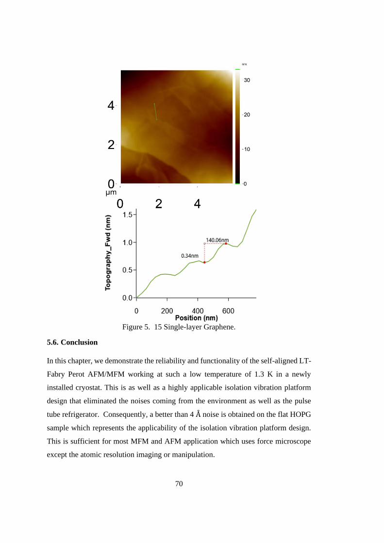
70
Figure 5. 15 Single-layer Graphene.
5.6. Conclusion
In this chapter, we demonstrate the reliability and functionality of the self-aligned LT-
Fabry Perot AFM/MFM working at such a low temperature of 1.3 K in a newly
installed cryostat. This is as well as a highly applicable isolation vibration platform
design that eliminated the noises coming from the environment as well as the pulse
tube refrigerator. Consequently, a better than 4 Å noise is obtained on the flat HOPG
sample which represents the applicability of the isolation vibration platform design.
This is sufficient for most MFM and AFM application which uses force microscope
except the atomic resolution imaging or manipulation.
71
CHAPTER 6
6. FABRY PEROT INTERFEROMETER
6.1. Introduction
Technically Michelson fiber interferometer has such a limitation in obtaining the
deflection with high sensitivity based on its intrinsic noise coming from shot noise.
The laser shot noise is a kind of electronic noise that occurs by a finite number of
photons that are carrying the energy and making statistical fluctuations in the
measurements. The impact of striking the electrons on the photodiode is the generation
of a photocurrent 𝑖.
𝑖 = 𝑆𝑃𝐷𝑃 6.1
𝑖 is proportional to the power P and 𝑆𝑃𝐷 is responsivity of photo photodetector. The
average root-mean-squared variation of the current noise is given by:
𝑖�̅�ℎ𝑜𝑡 = √2𝑒𝑆𝑃𝐷𝑃 (𝐴
𝐻𝑧0.5)
6.2
e is the electronic charge, 1.6x10⁻¹⁶ C. If this current passes through a resistor, RF, the
average root-mean-squared variation of the voltage noise is given by:
�̅�𝑠ℎ𝑜𝑡 = √2𝑒𝑆𝑃𝐷𝑃𝑅𝐹 (𝑉
𝐻𝑧0.5)
6.3
Obviously, increasing the optical power falling to the photodetector makes increase
the signal sensitivity with the same ratio. Despite that, the shot noise will be increased
by the ratio of the square root of the signal. Admittedly, the noise would be reduced
by increasing optical power. As a result, the fiber Fabry Perot interferometer (FFPI)
is developed according to this approach for the deflection sensor.
Principally, the FFPI is expected by two reflections, first from the fiber-air surface
interface and then the backside of the cantilever. In order to have a reflection from the
fiber surface, the end part of the fiber should be cleaved and then coated by TiO2.

72
Coating the fiber provides multiple reflections and respectively the interference
pattern in a much sensitive way that is detected by the photodetector.
There are few groups [69-74] that developed FFPI in the literature to obtain the high
sensitivity deflection sensor for the atomic resolution image. Technically, coating the
fiber end to increase the reflectivity and creating the parallel mirror system, adjusting
the fiber in the best position regarding the cantilever as close as possible, as well as
increasing the optical power falls on the photodetector are three critical points that are
raised from FFPI design. To achieve these basics the end of the fiber is cleaved and
then coated by suitable material, then a stick-slip approach mechanism is designed to
adjust the fiber in the gap between the fiber and cantilever, and finally a fiber optic
circulator in embedded inside the interferometer instead of a 2x2 coupler.
Figure 6. 1The fiber Fabry-Perot interferometer (FFPI) Schematic principal. To
increases, the ratio of the internal reflection of the fiber and provides multiple
reflections between two parallel mirrors the fiber end should be coated.
6.2. Fiber Coating
There are two major advantages of coating the fiber end from the optical view. Firstly,
coating the fiber end increase the bare reflectivity from 3% to 39-70 %, and secondly,
the cantilever and the fiber stays like two parallel mirror and multiple reflections can
occur among these two plates. Consequently, utilizing the Fabry-Perot interferometer

73
helps to increase the finesse, visibility and slope values that contribute to high-
resolution imaging.
6.2.1. Fiber coating with TiO2
To achieve the higher interference slope as well as higher quality factor values the
cleaved end of the fiber is coated with the reflectiveTiO2 [75]. Firstly, to cleave the
fiber end a high precision fiber cleaver (Fujikura CT-30) is used to get 2-3% bare
reflectivity. The next step is dipping the fiber end for a few seconds in Titanium (IV)
2-ethylhexyloxide solution which is diluted by xylene with the ratio of one to five and
then burning the fiber end with a propane torchlight. Within this process, the TiO2
would be coated on the fiber and provides a reflectivity of 15-30%. [75]
6.3. Fiber Slider
The importance of the LT Fabry-Perot AFM/MFM is obtaining a higher slope of the
interference pattern. This can be achieved by adjusting the fiber in the best position
regarding the cantilever in a distance between the fiber and the cantilever. Normally
in the design of the Michelson interferometer, the distance is fixed and around 30 µm
with a Ø19 µm laser spot size which keeps a secure distance for the tip replacements.
As the fiber is adjustable, moving the fiber towards the cantilever makes a laser spot
size smaller and be equal to the fiber core. Hence, the signal gain would be enhanced
at the interferometer. This is where the misalignments of the fiber and cantilever which
could be made by fabrication are such a drawback with causing a loss of the
interferometer signal.
6.3.1. Fiber Slider Design for Low Temperature
To achieve this purpose with a certain functionality at low temperature, the MFM
alignment holder is modified [49] in a way that fiber can slide toward the cantilever
and vice-versa.
Therefore, the new design resulted in improved reliability of the fiber nano positioner
that is established by three major impressions: (1) centralizing the cantilever tip at the

74
piezo tube; (2) enhancing the surface quality of the groves in which the ferrule is
sliding; (3) increasing the inertial mass of the fiber holder.
(a) (b) (c)
Figure 6. 2 Parts of the LT fiber slider. (a) MFM V-shaped holder, (b) ferrule
tubing made of Zirconia, and (c) PhBr Leaf spring.
According to the design, the zirconia tubing with Ø1 mm which is polished, placed on
the V-shape titanium holder part. Similarly, the titanium holder is perfectly polished
to have a pure and smooth surface due to eliminating any struggle during the ferrule
slid. The zirconia surface is sandwiched between the two-titanium surface and a leaf
spring surface that press the tubing for replacement precisely in one direction toward
the cantilever tip. All these processes have done under an optical microscope to have
an absolute alignment and reach the minimum cavity gap as described earlier. The
zirconia tubing has a 0.5 mm z-range gap to approach and retract to the cantilever.
Obviously, the alignment maintains the same interferometer signal that obtains for
repetitive motions.
The motion of the fiber is implemented by scanner piezo. Here the brass weight which
is mounted on the zirconia tubing has a vital role in generating a momentum of the
sliding part with an order of the magnitude. Without the additional weight on the
ferrule, the fraction below the 125 K stops the ferrule motion. The PPS (Polyphenylene
sulfide) part is designed to hold all the assembly and house the ferrule. Also, the ferrule
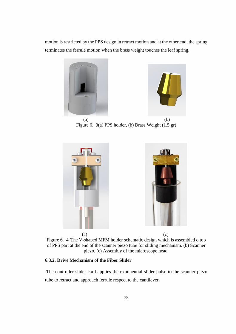
75
motion is restricted by the PPS design in retract motion and at the other end, the spring
terminates the ferrule motion when the brass weight touches the leaf spring.
(a) (b)
Figure 6. 3(a) PPS holder, (b) Brass Weight (1.5 gr)
(a) (c)
Figure 6. 4 The V-shaped MFM holder schematic design which is assembled o top
of PPS part at the end of the scanner piezo tube for sliding mechanism. (b) Scanner
piezo, (c) Assembly of the microscope head.
6.3.2. Drive Mechanism of the Fiber Slider
The controller slider card applies the exponential slider pulse to the scanner piezo
tube to retract and approach ferrule respect to the cantilever.

76
The figure below represents the ferrule tubing motion regarding the cantilever.
Normally, the motion is continued till the fiber touches the cantilever, then the ferrule
is retracted to find the maximum slope of the interference pattern.
Step 1: Gap ~ 600 μm Step 2: 300 μm
Step 3: 100 μm
Step 4: Gap < 1μm
Figure 6. 5 Fiber Approach by Stick-Slip Approach Mechanism.
6.3.3. Testing the Slip-Stick Mechanism at Low Temperature

77
(a)
(b)
Figure 6. 6Slider Piezo Step Length in 300K, 225K, 77K, 4K. (a) Forward motion,
(b) Backward motion.
The slider mechanism is examined and optimized in all operation temperature rages
successfully and represents a fully linear motion. Normally the applied voltage to the
y = 13.151x - 653.71R² = 1
y = 9.87x - 482R² = 0.9999
y = 6.5757x - 322.54R² = 1
y = 3.1385x - 88.009R² = 0.9802
0
500
1000
1500
2000
2500
3000
3500
4000
4500
5000
0 50 100 150 200 250 300 350 400 450
Fib
er P
osi
tio
n (
nm
)
voltage(V)
Forward Movement
4K
77K
225K
300K
y = 13.127x - 651.79R² = 1
y = 9.8205x - 472.61R² = 1
y = 6.585x - 324R² = 0.9999
y = 3.6208x - 175.08R² = 0.9807
0
500
1000
1500
2000
2500
3000
3500
4000
4500
5000
0 50 100 150 200 250 300 350 400 450
Fib
er P
osi
tio
n (
nm
)
voltage(V)
Backward Movement
4K
77K
225K
300K

78
slider should be increased by decreasing the temperature as the piezo capacitance is
dropping by the temperature drops.
The step sizes are tunable with adjusting the pulse height of the slider and controlling
the applied voltage in the software. The figure below presents an example of the
ferrule motion. The pattern was moved with a single approach step.
Figure 6. 7 Measuring fiber step on the interference pattern at 300 K. A single step
with 300 V height slider pulse applied for approaching. The red plot is the
interference pattern of the fiber position after one step moved toward the cantilever
which is measured 74 nm displacement.
6.3.4. Slope and Visibility Behavior vs gap distance between the Cantilever and
Fiber
As this is already mentioned, decreasing the gap makes the smaller laser spot and
increased signal gain that aims to increase the slope value of the interference pattern.
Here, the type of the cantilever is also important in increasing the reflectivity which
results in the higher slope value. Hence, each cantilever can provide a specific
maximum value of the slope. Besides, the visibility has unique behavior with a
maximum of 1 that does not change depends on the cantilever.
-0.2 0.0 0.2 0.4 0.6 0.8 1.0 1.2 1.4
100
200
300
400
500
600
Ph
oto
Dio
de P
ow
er
(μW
)
Fiber Position (μm)
Photo Diode Power
Photo Diode Power
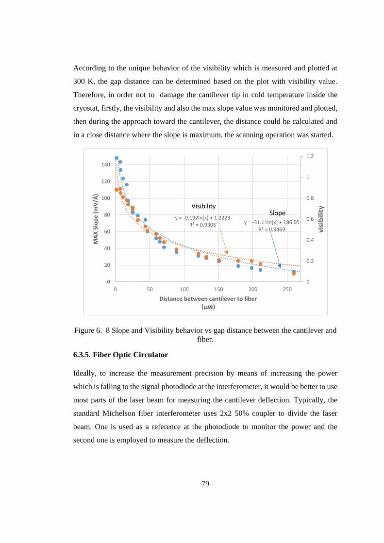
79
According to the unique behavior of the visibility which is measured and plotted at
300 K, the gap distance can be determined based on the plot with visibility value.
Therefore, in order not to damage the cantilever tip in cold temperature inside the
cryostat, firstly, the visibility and also the max slope value was monitored and plotted,
then during the approach toward the cantilever, the distance could be calculated and
in a close distance where the slope is maximum, the scanning operation was started.
Figure 6. 8 Slope and Visibility behavior vs gap distance between the cantilever and
fiber.
6.3.5. Fiber Optic Circulator
Ideally, to increase the measurement precision by means of increasing the power
which is falling to the signal photodiode at the interferometer, it would be better to use
most parts of the laser beam for measuring the cantilever deflection. Typically, the
standard Michelson fiber interferometer uses 2x2 50% coupler to divide the laser
beam. One is used as a reference at the photodiode to monitor the power and the
second one is employed to measure the deflection.
y = -31.11ln(x) + 186.05R² = 0.9469
y = -0.192ln(x) + 1.2223R² = 0.9306
0
0.2
0.4
0.6
0.8
1
1.2
0
20
40
60
80
100
120
140
0 50 100 150 200 250
visi
bili
ty
MA
X S
lop
e (
mV
/Ȧ)
Distance between cantilever to fiber(µ𝒎)
VisibilitySlope

80
To full fill this purpose the fiber optic circulator can be used which possibly utilizes
100% power. This is a non-reciprocal optical device with three ports that allow the
light to travel just in one direction.
Figure 6. 9 fiber optic circulator diagram for fiber interferometer [64].
The entering laser to port 1 will exit port 2, and in the way back the entering signal to
the port 2 will exit port 3.
Theoretically, utilizing the circulator [64] in the interferometer will enhance the
optical power 4 times that falls into the signal photodetector. This issue increases the
slope value, expectedly, in the same ratio.
Table 6. 1 The fiber optic circulator and the 2x2 coupler Comparison.
Slope (mV/Å) Power in the Fiber
(mW)
Circulator 120 3.0
2x2 50% Coupler 30 1.5
6.4. Fiber Fabry-Perot interferometer
The cleaved and coated end of the single-mode fiber will normally reflect 30-70% of
the laser light in the LT AFM/MFM system. The rest of the light passes the fiber end
to hit the cantilever back surface. The multiple reflections occur between these two
parallel mirrors. And increase the optical power on the photodetector as well as
increasing the internal reflectivity.
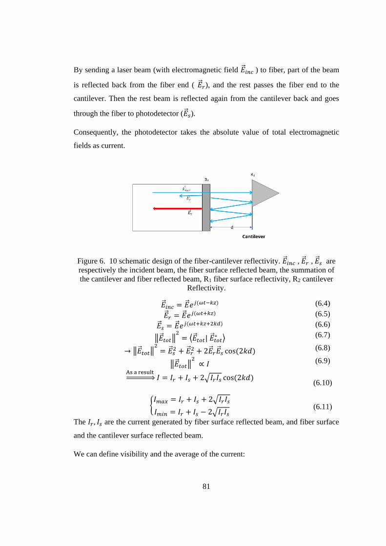
81
By sending a laser beam (with electromagnetic field �⃗� 𝑖𝑛𝑐 ) to fiber, part of the beam
is reflected back from the fiber end ( �⃗� 𝑟), and the rest passes the fiber end to the
cantilever. Then the rest beam is reflected again from the cantilever back and goes
through the fiber to photodetector (�⃗� 𝑠).
Consequently, the photodetector takes the absolute value of total electromagnetic
fields as current.
Figure 6. 10 schematic design of the fiber-cantilever reflectivity. �⃗� 𝑖𝑛𝑐 , �⃗� 𝑟 , �⃗� 𝑠 are
respectively the incident beam, the fiber surface reflected beam, the summation of
the cantilever and fiber reflected beam, R1 fiber surface reflectivity, R2 cantilever
Reflectivity.
�⃗� 𝑖𝑛𝑐 = �⃗� 𝑒𝑗(𝜔𝑡−𝑘𝑧) (6.4)
�⃗� 𝑟 = �⃗� 𝑒𝑗(𝜔𝑡+𝑘𝑧) (6.5)
�⃗� 𝑠 = �⃗� 𝑒𝑗(𝜔𝑡+𝑘𝑧+2𝑘𝑑) (6.6)
‖�⃗� 𝑡𝑜𝑡‖2= ⟨�⃗� 𝑡𝑜𝑡| �⃗� 𝑡𝑜𝑡
∗ ⟩ (6.7)
→ ‖�⃗� 𝑡𝑜𝑡‖2= �⃗� 𝑠
2 + �⃗� 𝑟2 + 2�⃗� 𝑟�⃗� 𝑠 cos(2𝑘𝑑)
(6.8)
‖�⃗� 𝑡𝑜𝑡‖2 ∝ 𝐼
(6.9)
As a result ⇒ 𝐼 = 𝐼𝑟 + 𝐼𝑠 + 2√𝐼𝑟𝐼𝑠 cos(2𝑘𝑑)
(6.10)
{𝐼𝑚𝑎𝑥 = 𝐼𝑟 + 𝐼𝑠 + 2√𝐼𝑟𝐼𝑠
𝐼𝑚𝑖𝑛 = 𝐼𝑟 + 𝐼𝑠 − 2√𝐼𝑟𝐼𝑠
(6.11)
The 𝐼𝑟 , 𝐼𝑠 are the current generated by fiber surface reflected beam, and fiber surface
and the cantilever surface reflected beam.
We can define visibility and the average of the current:
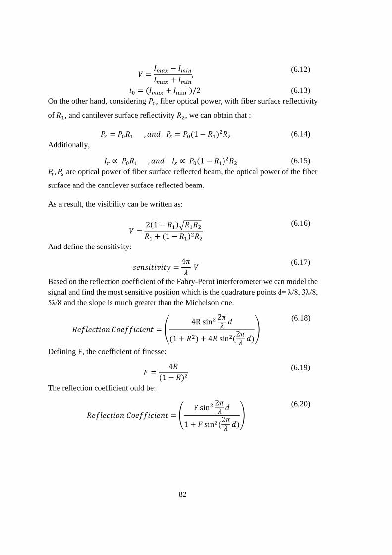
82
𝑉 =𝐼𝑚𝑎𝑥 − 𝐼𝑚𝑖𝑛𝐼𝑚𝑎𝑥 + 𝐼𝑚𝑖𝑛
, (6.12)
𝑖0 = (𝐼𝑚𝑎𝑥 + 𝐼min )/2 (6.13)
On the other hand, considering 𝑃0, fiber optical power, with fiber surface reflectivity
of 𝑅1, and cantilever surface reflectivity 𝑅2, we can obtain that :
𝑃𝑟 = 𝑃0𝑅1 , 𝑎𝑛𝑑 𝑃𝑠 = 𝑃0(1 − 𝑅1)2𝑅2 (6.14)
Additionally,
𝐼𝑟 ∝ 𝑃0𝑅1 , 𝑎𝑛𝑑 𝐼𝑠 ∝ 𝑃0(1 − 𝑅1)2𝑅2 (6.15)
𝑃𝑟 , 𝑃𝑠 are optical power of fiber surface reflected beam, the optical power of the fiber
surface and the cantilever surface reflected beam.
As a result, the visibility can be written as:
𝑉 =2(1 − 𝑅1)√𝑅1𝑅2𝑅1 + (1 − 𝑅1)2𝑅2
(6.16)
And define the sensitivity:
𝑠𝑒𝑛𝑠𝑖𝑡𝑖𝑣𝑖𝑡𝑦 =4𝜋
𝜆 𝑉
(6.17)
Based on the reflection coefficient of the Fabry-Perot interferometer we can model the
signal and find the most sensitive position which is the quadrature points d= λ/8, 3λ/8,
5λ/8 and the slope is much greater than the Michelson one.
𝑅𝑒𝑓𝑙𝑒𝑐𝑡𝑖𝑜𝑛 𝐶𝑜𝑒𝑓𝑓𝑖𝑐𝑖𝑒𝑛𝑡 = (4R sin2
2𝜋𝜆𝑑
(1 + 𝑅2) + 4𝑅 sin2(2𝜋𝜆𝑑))
(6.18)
Defining F, the coefficient of finesse:
𝐹 =4𝑅
(1 − 𝑅)2
(6.19)
The reflection coefficient ould be:
𝑅𝑒𝑓𝑙𝑒𝑐𝑡𝑖𝑜𝑛 𝐶𝑜𝑒𝑓𝑓𝑖𝑐𝑖𝑒𝑛𝑡 = (F sin2
2𝜋𝜆𝑑
1 + 𝐹 sin2(2𝜋𝜆𝑑))
(6.20)
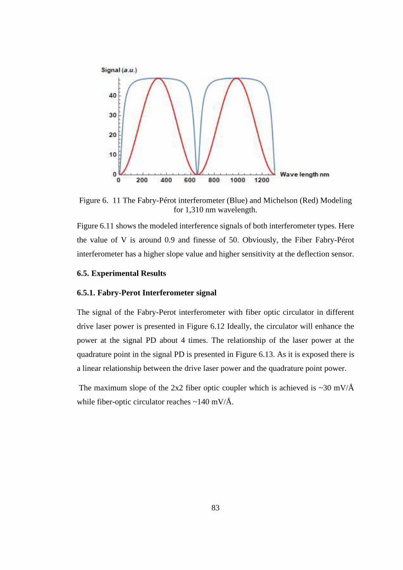
83
Figure 6. 11 The Fabry-Pérot interferometer (Blue) and Michelson (Red) Modeling
for 1,310 nm wavelength.
Figure 6.11 shows the modeled interference signals of both interferometer types. Here
the value of V is around 0.9 and finesse of 50. Obviously, the Fiber Fabry-Pérot
interferometer has a higher slope value and higher sensitivity at the deflection sensor.
6.5. Experimental Results
6.5.1. Fabry-Perot Interferometer signal
The signal of the Fabry-Perot interferometer with fiber optic circulator in different
drive laser power is presented in Figure 6.12 Ideally, the circulator will enhance the
power at the signal PD about 4 times. The relationship of the laser power at the
quadrature point in the signal PD is presented in Figure 6.13. As it is exposed there is
a linear relationship between the drive laser power and the quadrature point power.
The maximum slope of the 2x2 fiber optic coupler which is achieved is ~30 mV/Å
while fiber-optic circulator reaches ~140 mV/Å.
84
Figure 6. 12 Different drive laser power in the Fibre Fabry-Perot interferometer at
300 K.
Figure 6. 13 Representation of the Linear relationship between the interference
slope & Average power at quadrature point Vs drive laser power @ 300K.
The table below represents the difference interference slope obtained by different
interferometers.
Table 6. 2 Fabry-Perot and Michelson interferometers Comparison
Slope (mV/Å) Visibility Power (mW) Finesse
Fabry-Perot 148 0.9 3.5 4.4
Michelson 30 0.73 3.5 2.74
0
200
400
600
800
1000
0 0.2 0.4 0.6 0.8 1 1.2
Ph
oto
Dio
de
Po
wer
( μ
W)
Fiber Position (μm)
Photo Diode Power (500 μW)
Photo Diode Power (1000 μW)
Photo Diode Power (1500μW)
Photo Diode Power (2000 μW)
Photo Diode Power (2500 μW)
Photo Diode Power (3000 μW)
Photo Diode Power (3500μW)
Photo Diode Power(3700 mW)
0
20
40
60
80
100
120
0
100
200
300
400
500
600
0 1 2 3 4 5
Slo
pe
(mV
/Å)
Po
wer
at
the
qu
adra
ture
(m
W)
Laser Power (mW)
Power atthequadrature(mW)
Slope(mV/Å)
Linear(Power atthequadrature(mW))
Linear(Slope(mV/Å))

85
6.5.2. AFM Images:
To check the functionality of the microscope different samples in various temperatures
were recorded. Initially, the AFM image of the calibration grating Figure 6.14 is
recorded in 300 K. The interference pattern with a slope value of ~60 mV/Å was used
for this experiment. And the Q factor is 234.
In Figure 6.15, 6.16 depicts the tapping mode AFM image of the Graphite in both 300
K and 77 K with interference slope value of 52 mV/Å and Q factor of 482.
(a) (b)
(c)
Figure 6. 14 AFM image of the grating sample in Tapping mode at 300 K. (a)
Sample Topography, (b) Amplitude (Feedback) and, (c) Phase images.

86
(a) (b)
(c) (d)
Figure 6. 15 AFM image of the Graphite in Tapping mode at 300 K. (a)
Topography, (b) Amplitude (Feedback). (c) Graphite layers size.
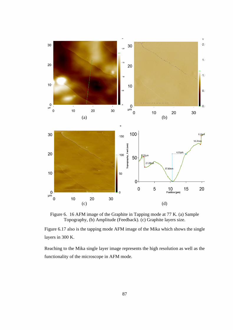
87
(a) (b)
(c) (d)
Figure 6. 16 AFM image of the Graphite in Tapping mode at 77 K. (a) Sample
Topography, (b) Amplitude (Feedback). (c) Graphite layers size.
Figure 6.17 also is the tapping mode AFM image of the Mika which shows the single
layers in 300 K.
Reaching to the Mika single layer image represents the high resolution as well as the
functionality of the microscope in AFM mode.
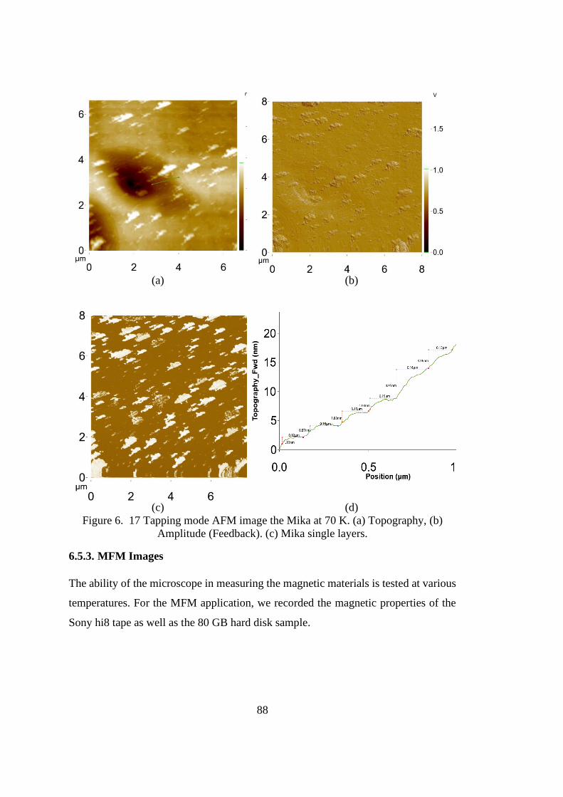
88
(a) (b)
(c) (d)
Figure 6. 17 Tapping mode AFM image the Mika at 70 K. (a) Topography, (b)
Amplitude (Feedback). (c) Mika single layers.
6.5.3. MFM Images
The ability of the microscope in measuring the magnetic materials is tested at various
temperatures. For the MFM application, we recorded the magnetic properties of the
Sony hi8 tape as well as the 80 GB hard disk sample.
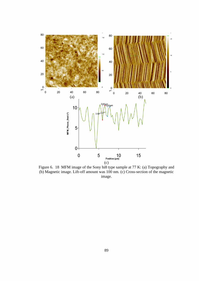
89
(a) (b)
(c)
Figure 6. 18 MFM image of the Sony hi8 type sample at 77 K: (a) Topography and
(b) Magnetic image. Lift-off amount was 100 nm. (c) Cross-section of the magnetic
image.
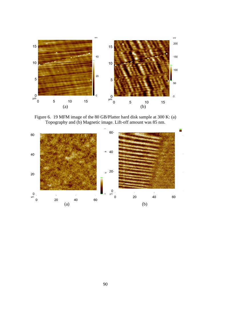
90
(a) (b)
Figure 6. 19 MFM image of the 80 GB/Platter hard disk sample at 300 K: (a)
Topography and (b) Magnetic image. Lift-off amount was 85 nm.
(a) (b)
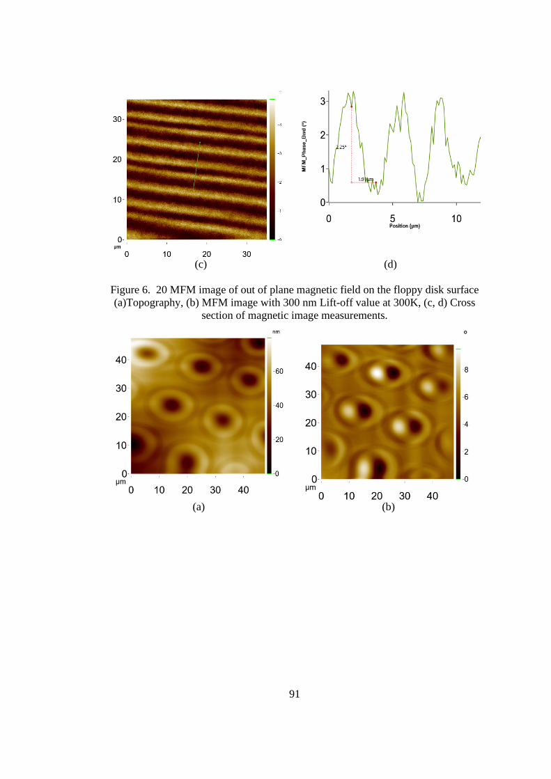
91
(c) (d)
Figure 6. 20 MFM image of out of plane magnetic field on the floppy disk surface
(a)Topography, (b) MFM image with 300 nm Lift-off value at 300K, (c, d) Cross
section of magnetic image measurements.
(a) (b)

92
(c) (d)
Figure 6. 21 Large laser bumps at the no load- unload ramps on the hard disk
surface also known as the landing zone for the head of the hard disk. (a, b)
Topography, and MFM image at 300 K, (c, d) Topography and MFM image at the
77 K.
6.5.4. Conclusions
We redesign and improve the LT Fabry-Perot AFM/MFM head by means of
increasing the reliability of fiber tubing movement in various temperature ranges of
300 K to 1.3 K. The functionality of slip-stick fiber slider is established and the new
design provides a better resolution with obtaining the higher interference slope value.
The new coating material benefits to enhance the reflectivity from the fiber surface
and implementing the mirror-like surface between the fiber end and cantilever in order
to increase the laser gain and lose much less. This is as well as utilizing the circulator
in the interferometer which contributes much less loss of the laser.

93
CHAPTER 7
7. CONCLUSION
In this thesis, we demonstrated a self-aligned low-temperature Fabry-Perot atomic
force/ magnetic force (LT-AFM/MFM) microscope with the ability of operation in
different temperatures from 300 K to 1.3 K. The alignment-free design provides the
compatibility of using different types of cantilevers as well as eliminating time-
consuming procedure for aligning the cantilever respect to the fiber with complicated
alignment setup. This microscope is exclusively designed for low-temperature
experiments and tried to reduce the outer dimension to be completely compatible with
various cryogenic systems.
For enhancing the reliability of the microscope operation, the head is redesigned and
modified. To achieve higher performance of fiber movement specifically in low
temperatures, the parts are altered and fully optimized. And the fiber end is coated by
TiO2 in order to increase the initial reflectivity from the fiber end and the laser gain in
the photodetector.
Redesigning the fiber nano positioner, enhancing the accuracy and optimizing the
parts provides reliable slip-stick operation in various temperatures and increased fiber
reflectivity to gain a higher slope value of the interference pattern.
The table below represents the critical Slope, Visibility and Finesse value where the
fiber positioned in a 1µm to the cantilever.
Table 7. 1 Slope, Visibility and Finesse value of old design Microscope
Old Design Power in the
Fibre (mW)
Slope (mV/Å) Visibility Finesse
Michelson
Interferometer
3.5 6 0.43 1.81
Fabry-Perot
Interferometer
3.5 120 0.89 4.31
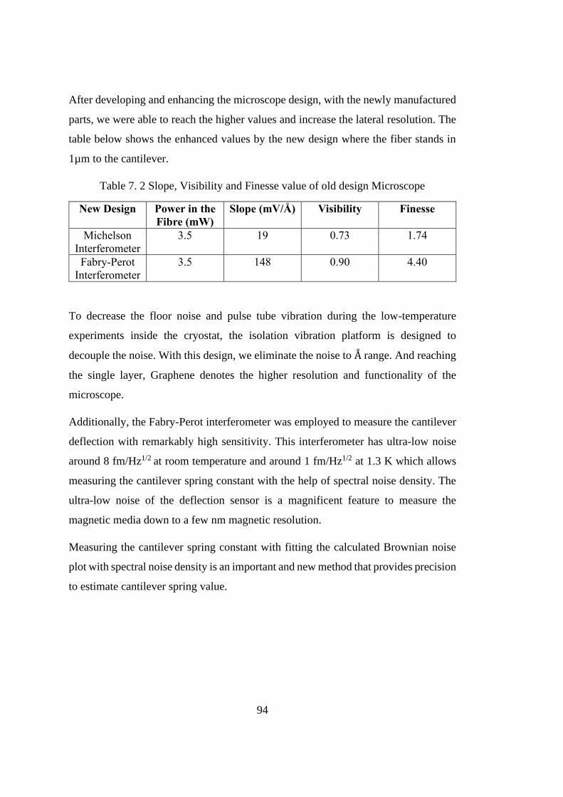
94
After developing and enhancing the microscope design, with the newly manufactured
parts, we were able to reach the higher values and increase the lateral resolution. The
table below shows the enhanced values by the new design where the fiber stands in
1µm to the cantilever.
Table 7. 2 Slope, Visibility and Finesse value of old design Microscope
New Design Power in the
Fibre (mW)
Slope (mV/Å) Visibility Finesse
Michelson
Interferometer
3.5 19 0.73 1.74
Fabry-Perot
Interferometer
3.5 148 0.90 4.40
To decrease the floor noise and pulse tube vibration during the low-temperature
experiments inside the cryostat, the isolation vibration platform is designed to
decouple the noise. With this design, we eliminate the noise to Å range. And reaching
the single layer, Graphene denotes the higher resolution and functionality of the
microscope.
Additionally, the Fabry-Perot interferometer was employed to measure the cantilever
deflection with remarkably high sensitivity. This interferometer has ultra-low noise
around 8 fm/Hz1/2 at room temperature and around 1 fm/Hz1/2 at 1.3 K which allows
measuring the cantilever spring constant with the help of spectral noise density. The
ultra-low noise of the deflection sensor is a magnificent feature to measure the
magnetic media down to a few nm magnetic resolution.
Measuring the cantilever spring constant with fitting the calculated Brownian noise
plot with spectral noise density is an important and new method that provides precision
to estimate cantilever spring value.

95
REFERENCES
[1] Hoffmann, R.; Baratoff, A.; Hug, H. J.; Hidber, H. R.; von Lohneysen, H.;
Guntherodt, H. J. G.,Mechanical manifestations of rare atomic jumps in dynamic force
microscopy. Nanotechnology 2007, 18 (39), 395503.
[2] Crampton, N.; Yokokawa, M.; Dryden, D. T. F.; Edwardson, J. M.; Rao, D. N.;
Takeyasu, K.; Yoshimura, S. H.; Henderson, R. M., Fast-scan atomic force
microscopy reveals that the type III restriction enzyme EcoP151 is capable of DNA
translocation and looping. Proceedings of the National Academy of Sciences of the
United States of America 2007, 104 (31), 12755–60.
[3] Ando, T.; Uchihashi, T.; Kodera, N.; Yamamoto, D.; Taniguchi, M.; Miyagi, A.;
Yamashita, H.,High-speed atomic force microscopy for observing dynamic
biomolecular processes. Journal of Molecular Recognition 2007, 20 (6), 448–58.
[4] Yokokawa, M.; Yoshimura, S. H.; Naito, Y.; Ando, T.; Yagi, A.; Sakai, N.;
Takeyasu, K., Fast scanning atomic force microscopy reveals the molecular
mechanism of DNA cleavage by Apal endonuclease. IEE Proceedings –
Nanobiotechnology 2006, 153 (4), 60–66.
[5] Becker, H.; Bender, O.; Bergmann, L.; Rost, K.; Zobel, A. Apparatus for
measuring surface irregularities. United States Patent number: 2728222, 1955.
[6] EATON, Peter; WEST, Paul. Atomic force microscopy. Oxford university press,
2010.
[7] Young, R.; Ward, J.; Scire, F., The topografiner: an instrument for measuring
surface microtopography. Review of Scientific Instruments 1972, 43 (7), 999–1011.
[8] G. Binning, H. Rohrer, Ch. Gerber and E. Weibel, Tunneling Through a
Controllable Vacuum Gap, Applied Physics Letter, 40, 178, 1982.

96
[9] G. Binning, H. Rohrer, Scanning Tunneling Microscopy, Helvetica Physica Acta,
55, 726-735, 1982.
[10] G. Binning, H. Rohrer, Ch. Gerber and E. Weibel, Surface Studies by Scanning
Tunneling Microscopy, Physical Review Letter, 49 (1), 57-61, 1982.
[11] Y. Yin, M. Zech, T. L. Williams and J. E. Hoffman, Scanning Tunneling
Microscopy and Spectroscopy on Iron-Pnictides, Physica C: Superconductivity, 469
(9-12), 535-544, 2009.
[12] Kano, S., Tada, T., & Majima, Y. (2015). Nanoparticle characterization based on
STM and STS. Chemical Society Reviews, 44(4), 970-987.
[13] Binnig, G.; Rohrer, H., Scanning tunneling microscopy. Helvetica Physica Acta
1982, 55 (6), 726–35.
[14] Binnig, G.; Rohrer, H., Scanning tunneling microscopy. Surface Science 1983,
126 (1–3), 236–44.
[15] F. F. Abraham, I. P. Batra, Theoretical Interpretation of Atomic Force
Microscope Images of Graphite, Surface Science, 209, 1989.
[16] R. G. Miller, P. J. Bryant, Atomic Force Microscopy of Layered Compounds,
Journal of Vacuum Science & Technology A, 7, 2879, 1989.
[17] T. R. Albrecht, P. Grütter, D. Horne and D. Rugar, Frequency Modulation
Detection Using HighQ Cantilevers for Enhanced Force Microscope Sensitivity,
Journal of Applied Physics, 69 (2), 668-673, 1991.
[18] Q. Zhong, D. Innis, K. Kjoller, V. B. Elings, Fractured Polymer/Silica Fibre
Surface Studied by Tapping Mode Atomic Force Microscopy, Surface Science, 290
(1-2), L688-L692, 1993.
97
[19] S. N. Magonov, V. Elings, M.-H. Whangbo, Phase Imaging and Stiffness in
Tapping-Mode Atomic Force Microscopy, Surface Science Letters, 375, L385-L391,
1997.
[20] Y. Martin and H. K. Wickramasinghe, Magnetic Imaging by Force Microscopy
With 1000 Å Resolution, Applied Physics Letter, 50 (20), 1455-1457, 1987.
[21] C. Israel, W. Wu and A. de Lozanne, High-Field Magnetic Force Microscopy as
Susceptibility Imaging, Applied Physics Letters, 89, 032502, 2006.
[22] A. Moser, H. J. Hug, I. Parashikov, B. Stiefel, O. Fritz, H. Thomas, A. Baratoff,
H. -J. Güntherodt and P. Chaudhari, Observation of Single Vortices Condensed into a
125 Vortex-Glass Phase by Magnetic Force Microscopy, Physical Review Letters,
74(10), 1847-1850, 1995.
[23] A. Volodin, K. Temst, A. Van Haesendonck, Y. Bruynseraede, M. I. Montero
and I. K. Schuller, Magnetic Force Microscopy of Vortices in Thin Niobium Films:
Correlation Between the Vortex Distribution and Thickness-Dependent Film
Morphology, Europhysics Letters, 58(4), 582-588, 2002.
[24] U. H. Pi, Z. G. Kim, D. H. Kim, A. Schwarz, M. Liebmann and R. Wiesendanger,
Dynamic Force Spectroscopy Across an Individual Strongly Pinned Vortex in a
Bi2Sr2CuCa2O8+δ Single Crystal, Applied Physics Letters, 85 (22), 5307-5309,
2004.
[25] M. Roseman and P. Grütter, Determination of Tc, Vortex Creation and Vortex
Imaging of a Superconducting Nb Film Using Low-Temperature Magnetic Force
Microscopy, Journal of Applied Physics, 91(10), 8840-8842, 2002.
[26] T. Shapoval, V. Neu, U. Wolff, R. Hühne, J. Hänisch, E. Backen, B. Holzapfel
and L. Schultz, Study of Pinning Mechanism in YBCO Thin Films by Means of
Magnetic Force Microscopy, Physica C, 460-462, 732-733, 2007.
98
[27] E.W. J. Straver, J. E. Hoffman, O. M. Auslaender, D. Rugar, and K. A. Moler,
Controlled Manipulation of Individual Vortices in a Superconductor, Applied Physics
Letters, 93, 172514, 2008.
[28] O. M. Auslaender, L. Luan, E. W. J. Straver, J. E. Hoffman, N. C. Koshnick, E.
Zeldov, D. A. Bonn, R. Liang, W. N. Hardy and K. A. Moller, Mechanics of
Individuals Isolated Vortices in a Cuprate Superconductor, Nature Physics, 5, 35-39,
2008.
[29] L. Luan, O. M. Auslaender, D. A. Bonn, R. Liang, W. N. Hardy and K. A. Moler,
Magnetic Force Microscopy Study of Interlayer Kinks in Individual Vortices in the
Underdoped Cuprate Superconductor YBa2Cu3O6+x, Physical Review B, 79,
214530, 2009.
[30] A. Schwarz, M. Liebmann, U. Kaiser and R. Wiesendanger, Visualization of the
Barkhausen Effect by Magnetic Force Microscopy, Physical Review Letters, 92(7),
077206, 2004.
[31] M. Liebmann, A. Schwarz, U. Kaiser, R. Wiesendanger, D.-W. Kim, and T. W.
Noh, Magnetization Reversal of a Structurally Disordered Manganite Thin Film with
Perpecdicular Anisotropy, Physical Review B, 71, 104431, 2005.
[32] W. Wu, C. Israel, N. Hur, S. Park, S. W. Cheong, and A. de Lozanne, Magnetic
Imaging of a Supercooling Glass Transition in a Weakly Disordered Ferromagnet,
Nature Materials, 5, 881-886, 2006.
[33] A.Lakhani, P. Kushwaha, R. Rawat and P. Chaddah, Magnetic Force Microscopic
Study of the Magnetic Field Induced Antiferro to Ferrimagnetic Transition in
Mn1.85Co0.15Sb, Applied Surface Science, 256(2), 404-406, 2009.
[34] P. Milde, D. Köhler, J. Seidel, L. M. Eng, A. Bauer, A. Chacon, J. Kindervater,
S. Mühlbauer, C. Pfleiderer, S. Buhrandt, C. Schütte, A. Rosch, Unwinding of a
Skyrmion Lattice by Magnetic Monopoles, Science, 340, 1076-1080, 2013.

99
[35] A. Schwarz and R. Wiesendanger, Magnetic Sensitive Force Microscopy,
Nanotoday, 3(1-2), 28-39, 2008.
[36] H. J. Hug, B. Steifel, P. J. A. van Schendel, A. Moser, S. Martin, and H.-J.
Güntherodt, A Low Temperature Ultrahigh Vacuum Scanning Force Microscope,
Review of Scientific Instruments, 70(9), 3625-3640, 1999.
[37] D. Rugar, H. J. Mamin and P. Guethner, Improved Fibre Optic Interferometer for
Atomic Force Microscopy, Applied Physics Letter, 55, 2588-2590, 1989. 127
[38] D. Rugar, H. J. Mamin, R. Erlandson, J. E. Stern and B. D. Terris, Force
Microscope Using a Fibre-Optic Displacement Sensor, Review of Scientific
Instruments, 59 (11), 2337-2340, 1988.
[39] A. Moser, H. J. Hug, Th. Jung, U. D. Schwarz and H-J. Güntherodt, A Miniature
Fibre Optic Force Microscope Scan Head, Measurement Science and Technology, 4,
769-775, 1993.
[40] Martin, Y.; Wickramasinghe, H. K., Magnetic imaging by force microscopy with
1000-A˚resolution. Applied Physics Letters 1987, 50 (20), 1455–57.
[41] Martin, Y.; Rugar, D.; Wickramasinghe, H. K., High-resolution magnetic
imaging of domains in TbFe by force microscopy. Applied Physics Letters 1988, 52
(3), 244–46.
[42] Mamin, H. J.; Rugar, D.; Stern, J. E.; Terris, B. D.; Lambert, S. E., Force
microscopy of magnetization patterns in longitudinal recording media. Applied
Physics Letters 1988, 53 (16), 1563–65.
[43] Abelmann, L.; Porthun, S.; Haast, M.; Lodder, C.; Moser, A.; Best, M. E.; van
Schendel, P.J. A.; Stiefel, B.; Hug, H. J.; Heydon, G. P.; Farley, A.; Hoon, S. R.;
Pfaffelhuber, T.; Proksch, R.; Babcock, K., Comparing the resolution of magnetic
force microscopes using the CAMST reference samples. Journal of Magnetism and
Magnetic Materials 1998, 190 (1–2), 135–47.

100
[44] Lin, C. W.; Fan, F.-R. F.; Bard, A. J., High resolution photoelectrochemical
etching of n-GaAs with the scanning electrochemical and tunneling microscope.
Journal of the Electrochemical Society 1987, 134 (4), 1038–39.
[45] Hosaka, S.; Kikukawa, A.; Honda, Y.; Hasegawa, T., Just-on-surface magnetic
force microscopy.Applied Physics Letters 1994, 65 (26), 3407–9.
[46] Mamin, H. J.; Rugar, D.; Stern, J. E.; Terris, B. D.; Lambert, S. E., Force
microscopy of magnetization patterns in longitudinal recording media. Applied
Physics Letters 1988, 53 (16), 1563–65.
[47] Porthun, S.; Abelmann, L.; Lodder, C., Magnetic force microscopy of thin film
media for high density magnetic recording. Journal of Magnetism and Magnetic
Materials 1998, 182 (1–2), 238–73.
[48] Schreiber, S.; Savla, M.; Pelekhov, D. V.; Iscru, D. F.; Selcu, C.; Hammel, P. C.;
Agarwal, G.,Magnetic force microscopy of superparamagnetic nanoparticles. Small
2008, 4 (2), 270–78.
[49] Karcı, Ö. (2015). Design of A Self-Aligned, High Resolution, Low Temperature
(30 Mk-300 K) Magnetic Force Microscope.
[50] Wittborn, J. (2000). Nanoscale studies of functional materials using scanning
probe microscopy (Doctoral dissertation, Materialvetenskap).
[51] Correa Orellana, A. (2018). Magnetic Force Microscopy study of layered
superconductors in vectorial magnetic fields.
[52] Peng Pan, Feiyu Yang, Zhenhua Wang, Bowen Zhong, Lining Sun, and Changhai
Ru. A Review of Stick–Slip Nanopositioning Actuators, pages 1–32. Springer
International Publishing, Cham, 2016.
[53]“PiezoelectricTubeScanners.”PiezoDrive,2019,www.piezodrive.com/actuators/p
iezoelectric-tube-scanners/.

101
[54] H. Kuramochi, T. Uzumaki, M. Yasutake, A. Tanaka, H. Akinaga and H.
Yokoyama, A Magnetic Force Microscope Using CoFe-Coated Carbon Nanotube
Probes, Nanotechnology, 16, 24-27, 2005.
[55] A. Winkler, T. Mühl, S. Menzel, R. K.-Koseva, S. Hampel, A. Leonhardt and B.
Büchner, Magnetic Force Microscopy Sensors Using Iron-Filled Carbon Nanotubes,
Journal of Applied Physics, 99, 104905, 2006.
[56] I. Utke, P. Hoffmann, R. Berger and L. Scandella, High-Resolution Magnetic Co
Supertips Grown by a Focused Electron Beam, Applied Physics Letters, 80(25), 4792-
4794, 2002.
[57] L. Gao, L. P. Yue, T. Yokota, R. Skomski, S. H. Liou, H. Takahoshi, H. Saito
and S. Ishio, Focused Ion Beam Milled CoPt Magnetic Force Microscopy Tips for
High Resolution Domian Images, IEEE Transactions on Magnetics, 40(4), 2194-
2196, 2004.
[58] L. M. Belova, O. Hellwig, E. Dobisz and E. D. Dahlberg, Rapid Preparation of
Electron Beam Induced Deposition Co Magnetic Force Microscopy Tips with 10 nm
Spatial Resolution, Review of Scientific Instruments, 83, 093711, 2012.
[59] O. Teschke, Micromagnetic Structure Images Taken Using Platinum Coated
Tips, Applied Physics Letters, 79(17), 2773-2775, 2001.
[60] Nanosensors Inc., Rue Jaquet- Droz 1, Case Postale 216, CH-2002, Neuchatel,
Switzerland
[61] Karcı, Ö., Dede, M., & Oral, A. (2014). Design of a self-aligned, wide
temperature range (300 mK-300 K) atomic force microscope/magnetic force
microscope with 10 nm magnetic force microscope resolution. Review of Scientific
Instruments, 85(10), 103705.
[62] T. Fukuma and S. P. Jarvis, Development of Liquid-Environment Frequency
Modulation Atomic Force Microscope with Low Noise Deflection Sensor for
102
Cantilevers of Various Dimensions, Review of Scientific Instruments, 77, 043701,
2006.
[63]TappingModeAFM, 019,www.nanophys.kth.se/nanophys/facilities/nfl/afm/fast-
scan/bruker-elp/Content/TappingMode%20AFM/TappingMode%20AFM.htm.
[64] Choi, S. J., Kim, K. H., Cho, Y. J., Cho, S. H., Kwon, S. J., Moon, J. H., & Lee,
K. J. (2010). Demonstration of ultra-high-resolution MFM images using Co90Fe10-
coated CNT probes. Journal of Magnetism and Magnetic Materials, 322(3), 332-336.
[65] 2019, www.physlab.org/wp-content/uploads/2016/04/VSM-Service-Manual-
Evacuating-and-Recharging-the-System-min.pdf.
[66] Banjare, Y. P. (2009). Theoretical and experimental studies on pulse tube
refrigerator (Doctoral dissertation).
[67] “Closed Cycle Cryocooler Principles of Operation.” Advanced Research ystems,
2019, www.arscryo.com/cryocooler-principles-of-operation.
[68] Newport Corp., S2000 Stabilizer Series.1791 Deere Avenue, Irvine, CA 92606,
United States.
[69] A. Oral, R. A. Grimble, H. Ö. Özer and J. B. Pethica, High-Sensitivity
NonContact Atomic Force Microscope/Scanning Tunneling Microscope (nc
AFM/STM) Operating at Subangstrom Oscillation Amplitudes for Atomic Resolution
Imaging and Force Spectroscopy, Review of Scientific Instruments, 74(8), 3656-3663,
2003.
[70] B. W. Hoogenboom, P. L. T. M. Frederix, J. L. Yang, S. Martin, Y. Pellmont, M.
Steinacher, S. Zäch, H. Heimbeck, A. Engel, and H. J. Hug, A Fabry–Perot
Interferometer for Micrometer-Sized Cantilevers, Applied Physics Letters, 86,
074101, 5–8, 2005.

103
[71] H. I. Rasool, P. R. Wilkinson, A. Z. Stieg, and J. K. Gimzewski, A Low Noise
All-Fibre Interferometer for High Resolution Frequency Modulated Atomic Force
Microscopy Imaging in Liquids, Review of Scientific Instruments, 81, 023703, 2010.
[72] B. W. Hoogenboom, P. L. T. M. Frederix, D. Fotiadis, H. J. Hug, and A. Engel,
Potential of Interferometric Cantilever Detection and Its Application for SFM/AFM
in Liquids, Nanotechnology, 19, 384019, 2008.
[73] D. T. Smith, J. R. Pratt, and L. P. Howard, A Fibre-Optic Interferometric with
Subpicometer Resolution for DC and Low-Frequency Displacement Measurement,
Review of Scientific Instruments, 80, 035105, 2009.
[74] H. Hölscher, P. Milde, U. Zerweck, L. M. Eng, and R. Hoffmann, The Effectiv
Quality Factor at Low Temperatures in Dynamic Force Microscopes with Fabry-Pérot
Interferometer Detection, Applied Physics Letters, 94, 223514, 2009.
[75] Subba-Rao, V., Sudakar, C., Esmacher, J., Pantea, M., Naik, R., & Hoffmann, P.
M. (2009). Improving a high-resolution fiber-optic interferometer through deposition
of a TiO 2 reflective coating by simple dip-coating. Review of Scientific
Instruments, 80(11), 115104.


105