Section 30. I/O Ports with Peripheral Pin Select...
38
© 2007-2012 Microchip Technology Inc. DS70190E-page 30-1 I/O Ports with Peripheral Pin 30 Section 30. I/O Ports with Peripheral Pin Select (PPS) HIGHLIGHTS This section contains the following major topics: 30.1 Introduction .................................................................................................................. 30-2 30.2 I/O Port Control Registers ............................................................................................ 30-3 30.3 Peripheral Multiplexing................................................................................................. 30-5 30.4 Peripheral Pin Select (PPS) ......................................................................................... 30-7 30.5 Change Notification (CN) Pins ................................................................................... 30-13 30.6 CN Operation in Sleep and Idle Modes ..................................................................... 30-14 30.7 Registers .................................................................................................................... 30-15 30.9 Related Application Notes.......................................................................................... 30-35 30.10 Revision History ......................................................................................................... 30-36
Transcript of Section 30. I/O Ports with Peripheral Pin Select...
Section 30. I/O Ports with Peripheral Pin Select (PPS)
I/O Ports w
ith Peripheral Pin
30
HIGHLIGHTSThis section contains the following major topics:
30.1 Introduction .................................................................................................................. 30-230.2 I/O Port Control Registers............................................................................................30-330.3 Peripheral Multiplexing.................................................................................................30-530.4 Peripheral Pin Select (PPS)......................................................................................... 30-730.5 Change Notification (CN) Pins ................................................................................... 30-1330.6 CN Operation in Sleep and Idle Modes ..................................................................... 30-1430.7 Registers.................................................................................................................... 30-1530.9 Related Application Notes..........................................................................................30-3530.10 Revision History .........................................................................................................30-36
© 2007-2012 Microchip Technology Inc. DS70190E-page 30-1
dsPIC33F/PIC24H Family Reference Manual
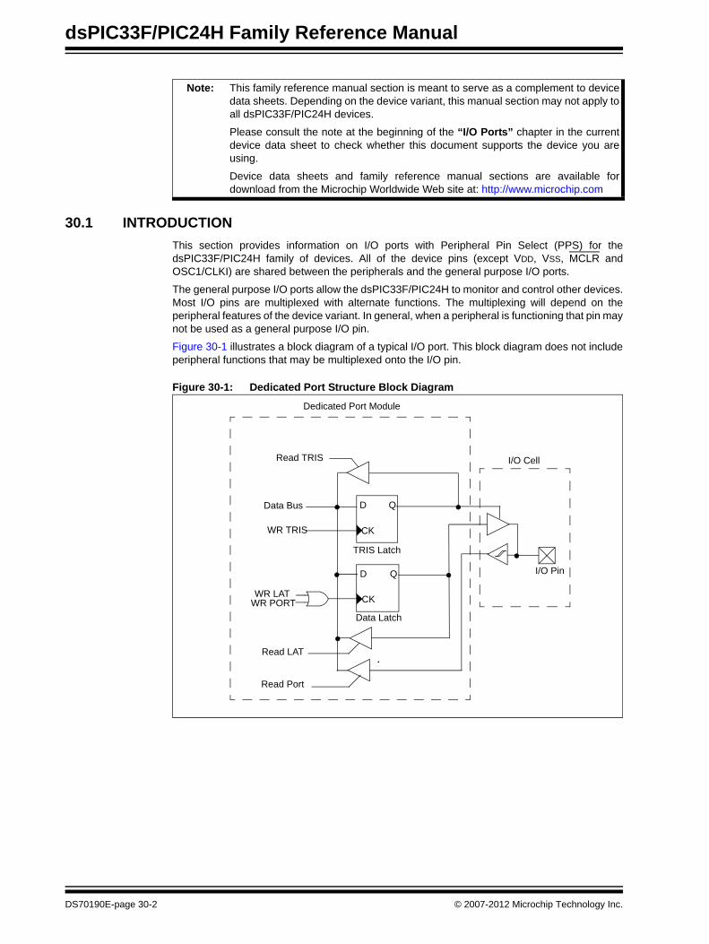
30.1 INTRODUCTIONThis section provides information on I/O ports with Peripheral Pin Select (PPS) for the dsPIC33F/PIC24H family of devices. All of the device pins (except VDD, VSS, MCLR and OSC1/CLKI) are shared between the peripherals and the general purpose I/O ports.
The general purpose I/O ports allow the dsPIC33F/PIC24H to monitor and control other devices. Most I/O pins are multiplexed with alternate functions. The multiplexing will depend on the peripheral features of the device variant. In general, when a peripheral is functioning that pin may not be used as a general purpose I/O pin.
Figure 30-1 illustrates a block diagram of a typical I/O port. This block diagram does not include peripheral functions that may be multiplexed onto the I/O pin.
Figure 30-1: Dedicated Port Structure Block Diagram
Note: This family reference manual section is meant to serve as a complement to device data sheets. Depending on the device variant, this manual section may not apply to all dsPIC33F/PIC24H devices.
Please consult the note at the beginning of the “I/O Ports” chapter in the current device data sheet to check whether this document supports the device you are using.
Device data sheets and family reference manual sections are available for download from the Microchip Worldwide Web site at: http://www.microchip.com
QD
CK
WR LAT
TRIS Latch
I/O Pin
WR PORT
Data Bus
QD
CK
Data Latch
Read LAT
Read Port
Read TRIS
WR TRIS
I/O Cell
Dedicated Port Module
DS70190E-page 30-2 © 2007-2012 Microchip Technology Inc.

Section 30. I/O Ports with Peripheral Pin Select (PPS)I/O
Ports with
Peripheral Pin
30
30.2 I/O PORT CONTROL REGISTERSAll I/O ports have the following four registers directly associated with the operation of the port, where ‘x’ denotes the particular I/O port.
• TRISx: Data Direction register• PORTx: I/O Port register• LATx: I/O Latch register• ODCx: Open-Drain Control register
Each I/O pin on the device has an associated bit in the TRIS, PORT and LAT registers.
30.2.1 TRIS RegistersThe TRISx register control bits determine whether each pin associated with the I/O port is an input or an output. If the TRIS bit for an I/O pin is ‘1’, then the pin is configured as an input. If the TRIS bit for an I/O pin is ‘0’, then the pin is configured as an output. An easy way to remember this is that a ‘1’ looks like an I (input) and a ‘0’ looks like an O (output). After a Reset all port pins are defined as inputs.
30.2.2 PORT RegistersData on an I/O pin is accessed through a PORTx register. A read of the PORTx register reads the value of the I/O pin, while a write to the PORTx register writes the value to the port data latch.
Many instructions, such as the BSET and BCLR instructions are read-modify-write operations. Therefore, a write to a port implies that the port pins are read, this value is modified, and then it is written to the port data latch. Care should be taken when read-modify-write commands are used on the PORTx registers and when I/O pins associated with the port are configured as inputs. If an I/O pin configured as an input is later changed to an output, an unexpected value may be output on the I/O pin. This effect occurs because the read-modify-write instruction reads the instantaneous value on the input pin and loads that value into the port data latch.
In addition, if read-modify-write instructions are used on the PORTx registers while I/O pins are configured as output, unintended I/O behavior may occur based on the device speed and I/O capacitive loading. Figure 30-2 illustrates unintended behavior that occurs if the user application attempts to set I/O bits 0 and 1 on PORTA with two consecutive read-modify-write instructions in the PORTA register. At high CPU speeds and high capacitive loading on the I/O pins, the unintended result of the example code is that only I/O bit 1 is set high.
Figure 30-2: Example of Unintended I/O Behavior
Note: The total number of ports and available I/O pins depend on the specific device. In a given device, all of the bits in a port control register may not be implemented. For more information, refer to the “I/O Ports” chapter in the specific device data sheet.
I/O Pin 1 Voltage
I/O Pin 0 Voltage
1
23
4BSET PORTA, #O instruction has finished execution. Voltage on I/O Pin 0 is starting to rise.
BSET PORTA, #1 instruction starts execution and reads PORTA register (bit 0 is read as ‘0’).
I/O pin 0 transitions from ‘0’ to ‘1’.
BSET PORTA, #1 instruction has finished execution. Voltage is starting to rise on I/O pin 1 and fall on I/O pin 0.
Example Code:BSET PORTA, #0 ; Set pin 0 on Port A to ‘1’BSET PORTA, #1 ; Set pin 1 on Port A to ‘1’
© 2007-2012 Microchip Technology Inc. DS70190E-page 30-3

dsPIC33F/PIC24H Family Reference Manual
In step 1 of Figure 30-2, when the first BSET instruction is executed, it writes a ‘1’ to bit 0 in the PORTA register, which raises the voltage level on the pin 0 to logic level 1. However, if the second BSET instruction is executed before the voltage level on pin 0 has reached the threshold for logic 1 (step 3 in Figure 30-2), the second BSET (read-modify-write) instruction reads ‘0’ for bit 0, which it writes back into the PORTA register (step 2 in Figure 30-2). In other words, instead of reading a value of 0x0001 from the PORTA register, it reads a value of 0x0000, modifies it to 0x0002 (instead of the desired value of 0x0003) and then writes that value back to the PORTA register. This causes the voltage on pin 0 to start falling to logic level 0 and the voltage on pin 1 to start rising to logic level 1, as illustrated in step 4 in Figure 30-2.
30.2.3 LAT RegistersThe LATx register associated with an I/O pin eliminates the problems that could occur with read-modify-write instructions. A read of the LATx register returns the values held in the port output latches instead of the values on the I/O pins. A read-modify-write operation on the LAT register associated with an I/O port avoids the possibility of writing the input pin values into the port latches. A write to the LATx register has the same effect as a write to the PORTx register. Example 30-1 uses the LATx register to set two I/O bits.
Example 30-1: Setting I/O Pins with the LATx Register
The differences between the PORTx and LATx registers can be summarized as follows:
• A write to the PORTx register writes the data value to the port latch• A write to the LATx register writes the data value to the port latch• A read of the PORTx register reads the data value on the I/O pin• A read of the LATx register reads the data value held in the port latch
Any bit and its associated data and control registers that are not valid for a particular device will be disabled, which means the corresponding LATx and TRISx registers and the port pin will be read as ‘0’.
30.2.4 Open-Drain Control RegistersIn addition to the PORT, LAT and TRIS registers for data control, each port pin can also be individually configured for either digital or open-drain output. This is controlled by the Open-Drain Control register, ODCx, associated with each port. Setting any of the bits configures the corresponding pin to act as an open-drain output.
The open-drain feature allows the generation of outputs higher than VDD (for example, 5V) on any desired digital-only pins by using external pull-up resistors. The open-drain I/O feature is not supported on pins that have analog functionality multiplexed on the pin. The maximum open-drain voltage allowed is the same as the maximum VIH specification. The open-drain output feature is supported for both port pin and peripheral configurations.
BSET LATA, #0 ;Set pin 0 on Port A to ‘1’BSET LATA, #1 ;Set pin 1 on Port A to ‘1’
DS70190E-page 30-4 © 2007-2012 Microchip Technology Inc.

Section 30. I/O Ports with Peripheral Pin Select (PPS)I/O
Ports with
Peripheral Pin
30
30.3 PERIPHERAL MULTIPLEXINGWhen a peripheral is enabled, the associated pin output drivers are typically module controlled, while a few are user-settable. The term “user-settable” means that the pin output driver is user-configurable.The I/O pin may be read through the input data path, but the output driver for the I/O port bit is generally disabled.
An I/O port that shares a pin with another peripheral is always subservient to the peripheral. The peripheral’s output buffer data and control signals are provided to a pair of multiplexers. The multiplexers select whether the peripheral or the associated port has ownership of the output data and control signals of the I/O pin. Figure 30-3 illustrates how ports are shared with other peripherals and the associated I/O pin to which they are connected.
Figure 30-3: Shared Port Structure Block Diagram
30.3.1 I/O Multiplexing with Multiple PeripheralsFor some dsPIC33F/PIC24H devices, particularly those with a small number of I/O pins, multiple peripheral functions may be multiplexed on each I/O pin. Figure 30-3 illustrates an example of two peripherals multiplexed to the same I/O pin.
The name of the I/O pin defines the priority of each function associated with the pin. The conceptual I/O pin illustrated in Figure 30-3 has two multiplexed peripherals, Peripheral A and Peripheral B, and is named PERA/PERB/PIO. The user application can easily determine the pri-ority of the functions assigned to the pin by the I/O pin name. As illustrated in Figure 30-3, Periph-eral A has the highest priority for control of the pin. If Peripheral A and Peripheral B are enabled at the same time, Peripheral A will take control of the I/O pins.
Note: Some ports are shared with ADC module pins. The corresponding bits in the AD1PCFG and AD2PCFG registers, if present, must be set to ‘1’ for I/O port functionality, even if the ADC module is turned off.
QD
CK
TRIS Latch
Data Bus
QD
CKData Latch
Read LAT
Read Port
Read TRIS
WR TRIS
PIO Module
WR LATWR Port
0
1Peripheral A o.e.
0
1
Peripheral A EnablePeripheral B Enable
Peripheral B o.e.
0
1Peripheral A Data
0
1Peripheral B Data
RPeripheral A Input
RPeripheral B Input
PERA/PERB/PIO
Peripheral Multiplexers
I/O Pin
© 2007-2012 Microchip Technology Inc. DS70190E-page 30-5

dsPIC33F/PIC24H Family Reference Manual
30.3.1.1 SOFTWARE INPUT PIN CONTROL
Some of the functions assigned to an I/O pin may be input functions that do not take control of the pin output driver. An example of one such peripheral is the Input Capture module. If the I/O pin associated with the Input Capture is configured as an output using the appropriate TRIS control bit, the user can manually affect the state of the Input Capture pin through its corresponding PORT register. This behavior can be useful in some situations, particularly for testing purposes when no external signal is connected to the input pin.
Referring to Figure 30-3, the organization of the peripheral multiplexers will determine if the peripheral input pin can be manipulated in software using the PORT register. The conceptual peripherals illustrated in Figure 30-3 disconnect the PORT data from the I/O pin when the peripheral function is enabled.
In general, the following peripherals allow their input pins to be controlled manually through the PORT registers:
• External Interrupt pins• Timer Clock Input pins• Input Capture pins• PWM Fault pins
Most serial communication peripherals, when enabled, take control of the I/O pin so that the input pins associated with the peripheral cannot be affected through the corresponding PORT registers. These peripherals include the following:
• SPI• I2CTM
• DCI• UART• ECANTM
• QEI
30.3.1.2 PIN CONTROL SUMMARY
When a peripheral is enabled, the associated pin output drivers are typically module controlled, while a few are user-settable. The term “module control” means that the associated port pin output driver is disabled and the pin can only be controlled and accessed by the peripheral. The term “user-settable” means that the associated peripheral port pin output driver is user-configurable in software through the associated TRISx Special Function Register (SFR). The TRISx register must be set for the peripheral to function properly. For “user settable” peripheral pins, the actual port pin state can always be read through the PORTx SFR.
An Input Capture peripheral is a good example of a user-settable peripheral. The user application must write the associated TRIS register to configure the Input Capture pin as an input. As the I/O pin circuitry is active when the Input Capture is enabled, the following method can be used to manually capture events using software:
• The Input Capture pin is configured as an output using the associated TRIS register• Then, the software can write values to the corresponding LAT register drive to internally
control the Input Capture pin and force capture events
As another example, an INTx pin can be configured as an output, and then, by writing to the associated LATx bit, an INTx interrupt, if enabled, can be generated.
The UART is an example of a module control peripheral. When the UART is enabled, the PORT and TRIS registers have no effect and cannot be used to read or write the RX and TX pins. Most communication peripheral functions available on the dsPIC33F/PIC24H are module control peripherals.
For example, the SPI module can be configured for Master mode, in which only the SDO pin is required. In this example, the SDI pin can be configured as a general purpose output pin by clearing (setting to a logic ‘0’) the associated TRISx bit. For more information on how pins can be configured for a module, refer to that specific module section.
Note: Some peripherals may not be present on all device variants. For more information,refer to the related chapter in the specific device data sheet.
DS70190E-page 30-6 © 2007-2012 Microchip Technology Inc.

Section 30. I/O Ports with Peripheral Pin Select (PPS)I/O
Ports with
Peripheral Pin
30
30.4 PERIPHERAL PIN SELECT (PPS)A major challenge in general-purpose devices is providing the largest possible set of peripheral features while minimizing the conflict of features on I/O pins. The challenge is even greater on low pin-count devices. In an application where more than one peripheral needs to be assigned to a single pin, inconvenient work arounds in application code or a complete redesign may be the only option.
PPS configuration provides an alternative to these choices by enabling peripheral set selection and their placement on a wide range of I/O pins. By increasing the pinout options available on a particular device, users can tailor the device to their entire application, rather than trimming the application to fit the device.
The PPS configuration feature operates over a fixed subset of digital I/O pins. Users may independently map the input and/or output of most digital peripherals to any one of these I/O pins. PPS is performed in software and generally does not require the device to be reprogrammed. Hardware safeguards are included to prevent accidental or spurious changes to the peripheral mapping after it has been established.
30.4.1 Available PinsThe PPS feature is used with a range of up to 16 pins. The number of available pins depends on the particular device and its pin count. Pins that support the PPS feature include the designation “RPn” in their full pin designation, where “RP” designates a remappable peripheral and “n” is the remappable pin number.
30.4.2 Available PeripheralsThe peripherals managed by PPS are all digital-only peripherals. These include general serial communications (UART and SPI), general-purpose timer clock inputs, timer-related peripherals (Input Capture and Output Compare) and interrupt-on-change inputs.
In comparison, some digital-only peripheral modules are never included in the PPS feature. This is because the peripheral’s function requires special I/O circuitry on a specific port and cannot be easily connected to multiple pins. These modules include I2C. A similar requirement excludes all modules with analog inputs, such as the Analog-to-Digital Converter (ADC).
The key difference between remappable and non-remappable peripherals is that remappable peripherals are not associated with a default I/O pin. The peripheral must always be assigned to a specific I/O pin before it can be used. In contrast, non-remappable peripherals are always available on a default pin, assuming that the peripheral is active and not conflicting with another peripheral.
When a remappable peripheral is active on a given I/O pin, it takes priority over all other digital I/O and digital communication peripherals associated with the pin. Priority is given regardless of the type of peripheral that is mapped. Remappable peripherals never take priority over any analog functions associated with the pin.
30.4.3 Controlling PPSPPS features are controlled through two sets of SFRs: one to map peripheral inputs, and the other to map outputs. As the two SFRs are separately controlled, a particular peripheral’s input and output (if the peripheral has both) can be placed on any selectable function pin without constraint.
The association of a peripheral to a peripheral-selectable pin is handled in two different ways, depending on whether an input or output is being mapped.
Note: For a specific list of PPS supported peripherals, refer to the specific device data sheet.
© 2007-2012 Microchip Technology Inc. DS70190E-page 30-7

dsPIC33F/PIC24H Family Reference Manual
30.4.3.1 INPUT MAPPING
The inputs of the PPS options are mapped on the basis of the peripheral. The control register associated with a peripheral dictates the pin it will be mapped to. The RPINRx registers are used to configure peripheral input mapping (see Register 30-5 through Register 30-17). Each register contains sets of 5-bit fields, with each set associated with one of the remappable peripherals. Programming a given peripheral’s bit field with an appropriate 5-bit value maps the RPn pin with the corresponding value to that peripheral. For any given device, the valid range of values for any bit field corresponds to the maximum number of peripheral pin selections supported by the device. For example, Figure 30-4 illustrates remappable pin selection for the U1RX input.
Figure 30-4: Remappable Input for U1RX
Table 30-1: Selectable Input Sources (Maps Input to Function)
RP0
RP1
RP2
Vss
0
31
1
2 U1RX input
U1RXR<4:0>
to peripheral
RP3030
Input Name(1) Function Name Register Configuration BitsExternal Interrupt 1 INT1 RPINR0 INT1R<4:0>External Interrupt 2 INT2 RPINR1 INT2R<4:0>Timer2 External Clock T2CK RPINR3 T2CKR<4:0>Timer3 External Clock T3CK RPINR3 T3CKR<4:0>Input Capture 1 IC1 RPINR7 IC1R<4:0>Input Capture 2 IC2 RPINR7 IC2R<4:0>Input Capture 7 IC7 RPINR10 IC7R<4:0>Input Capture 8 IC8 RPINR10 IC8R<4:0>Output Compare Fault A OCFA RPINR11 OCFAR<4:0>PWM1 Fault FLTA1 RPINR12 FLTA1R<4:0>PWM2 Fault FLTA2 RPINR13 FLTA2R<4:0>QEI Phase A QEA RPINR14 QEAR<4:0>QEI Phase B QEB RPINR14 QEBR<4:0>QEI Index INDX RPINR15 INDXR<4:0>UART1 Receive U1RX RPINR18 U1RXR<4:0>UART1 Clear to Send U1CTS RPINR18 U1CTSR<4:0>SPI1 Data Input SDI1 RPINR20 SDI1R<4:0>SPI1 Clock Input SCK1 RPINR20 SCK1R<4:0>SPI1 Slave Select Input SS1 RPINR21 SS1R<4:0>Note 1: Unless otherwise noted, all inputs use the Schmitt input buffers.
Note: Table 30-1 and Figure 30-4 provide examples of selectable input sources for a generic device. For more information, refer to the specific device data sheet.
DS70190E-page 30-8 © 2007-2012 Microchip Technology Inc.

Section 30. I/O Ports with Peripheral Pin Select (PPS)I/O
Ports with
Peripheral Pin
30
30.4.3.2 OUTPUT MAPPING
In contrast to inputs, the outputs of the PPS options are mapped on the basis of the pin. In this case, a control register associated with a particular pin dictates the peripheral output to be mapped. The RPORx registers are used to control output mapping. Like the RPINRx registers, each register contains sets of 5-bit fields, with each set associated with one RPn pin (see Register 30-18 through Register 30-25). The value of the bit field corresponds to one of the peripherals, and that peripheral’s output is mapped to the pin (see Table 30-2 and Figure 30-5).
A null output is associated with the output register reset value of ‘0’. This is done to ensure that remappable outputs remain disconnected from all output pins by default.
Figure 30-5: Multiplexing of Remappable Output for RPn
Table 30-2: Output Selection for Remappable Pin (RPn)
30.4.3.3 MAPPING LIMITATIONS
The control schema of the peripheral select pins is not limited to a small range of fixed peripheral configurations. There are no mutual or hardware-enforced lockouts between any of the peripheral mapping SFRs. Usually, any combination of peripheral mappings across any or all of the RPn pins is possible. This includes both many-to-one and one-to-many mappings of peripheral inputs and outputs to pins. While such mappings may be technically possible from a configuration point of view, they may not be supportable from an electrical point of view.
Function RPnR<4:0> Output Name
NULL 00000 RPn tied to default port pinU1TX 00011 RPn tied to UART1 Transmit
U1RTS 00100 RPn tied to UART1 Ready to SendSDO1 00111 RPn tied to SPI1 Data Output
SCK1OUT 01000 RPn tied to SPI1 Clock OutputSS1OUT 01001 RPn tied to SPI1 Slave Select Output
OC1 10010 RPn tied to Output Compare 1OC2 10011 RPn tied to Output Compare 2
UPDN 11010 RPn tied to QEI direction (UPDN) status
Note: Figure 30-5 and Table 30-2 provide examples of a generic device. For more information, refer to the specific device data sheet.
RPnR<4:0>
0
x
3
Default
U1TX Output
U1RTS Output 4
UPDN Output
19OC2 Output
Output DataRPn
© 2007-2012 Microchip Technology Inc. DS70190E-page 30-9

dsPIC33F/PIC24H Family Reference Manual
30.4.4 Controlling Configuration ChangesPeripheral mapping can be changed during run time, Because of this, some restrictions on peripheral remapping are needed to prevent accidental configuration changes. All dsPIC33F/PIC24H devices include three features to prevent alterations to the peripheral map:
• Control register lock sequence• Continuous state monitoring• Configuration bit remapping lock
30.4.4.1 CONTROL REGISTER LOCK
Under normal operation, writes to the RPINRx and RPORx registers are not allowed. Attempted writes will appear to execute normally, but the contents of the registers will remain unchanged. To change these registers, the registers must be unlocked in hardware. The register lock is controlled by the IOLOCK bit (OSCCON<6>). Setting the IOLOCK bit prevents writes to the control registers and clearing the IOLOCK bit allows writes.
To set or clear the IOLOCK bit, a specific command sequence must be executed:
1. Write 0x46 to OSCCON<7:0>2. Write 0x57 to OSCCON<7:0>3. Clear (or set) IOLOCK as a single operation
The IOLOCK bit remains in one state until changed. This allows all of the peripheral pin selects to be configured with a single unlock sequence followed by an update to all of the control regis-ters. After this, the IOLOCK bit can be set with a second lock sequence.
30.4.4.2 CONTINUOUS STATE MONITORING
In addition to being protected from direct writes, the contents of the RPINRx and RPORx registers are constantly monitored in hardware by shadow registers. If an unexpected change in any of the registers occurs (like cell disturbances caused by ESD or other external events), a configuration mismatch reset will be triggered.
30.4.4.3 CONFIGURATION BIT PIN SELECT LOCK
As an additional level of safety, the device can be configured to prevent more than one write session to the RPINRx and RPORx registers. The IOL1WAY Configuration bit (FOSC<5>) blocks the IOLOCK bit from being cleared after it has been set once.
In the default (unprogrammed) state, IOL1WAY is set, restricting users to one write session. Programming IOL1WAY allows users unlimited access (with the use of the unlock sequence) to the PPS registers.
Note: MPLAB® C30 provides built-in C language functions for unlocking the OSCCON register:
__builtin_write_OSCCONL(value) __builtin_write_OSCCONH(value)
See the MPLAB help files for more information.
DS70190E-page 30-10 © 2007-2012 Microchip Technology Inc.

Section 30. I/O Ports with Peripheral Pin Select (PPS)I/O
Ports with
Peripheral Pin
30
30.4.5 Considerations for Peripheral Pin SelectionThe ability to control peripheral pin selection introduces several considerations into application design that most users would never think of otherwise. This is particularly true for several common peripherals, which are only available as remappable peripherals.
The main consideration is that the peripheral pin selects are not available on default pins in the device’s default (reset) state. Specifically, because all RPINRx registers reset to all 1’s and RPORx registers reset to 0’s, this means all PPS inputs are tied to VSS, while all PPS outputs are disconnected. This means that before any other application code is executed, the user must initialize the device with the proper peripheral configuration. As the IOLOCK bit resets in the unlocked state, it is not necessary to execute the unlock sequence after the device has come out of reset. For application safety, however, it is always advisable to set IOLOCK bit and lock the configuration after writing to the control registers.
The unlock sequence must be executed as an assembly-language routine, in the same manner as changes to the oscillator configuration, because the unlock sequence is timing critical. If the bulk of the application is written in C or another high-level language, the unlock sequence should be performed by writing in-line assembly.
Choosing the configuration requires the review of all peripheral pin selects and their pin assignments, particularly those that will not be used in the application. In all cases, unused pin selectable peripherals should be disabled completely. Unused peripherals should have their inputs assigned to an unused RPn pin function. I/O pins with unused RPn functions should be configured with the null peripheral output.
The assignment of a peripheral to a particular pin does not automatically perform any other configuration of the pin’s I/O circuitry. In theory, this means adding a pin selectable output to a pin may mean inadvertently driving an existing peripheral input when the output is driven. Users must be familiar with the behavior of other fixed peripherals that share a remappable pin and know when to enable or disable them. To be safe, fixed digital peripherals that share the same pin should be disabled when not in use.
Along these lines, configuring a remappable pin for a specific peripheral does not automatically turn that feature on. The peripheral must be specifically configured for operation and enabled as if it were tied to a fixed pin. Where this happens in the application code (immediately following device reset and peripheral configuration, or inside the main application routine), depends on the peripheral and its use in the application.
A final consideration is that PPS functions neither override analog inputs nor reconfigure pins with analog functions for digital I/O. If a pin is configured as an analog input on device Reset, it must be explicitly reconfigured as a digital I/O when used with PPS. Example 30-2 illustrates a configuration for bidirectional communication with flow control using UART1. The following input and output functions are used:
• Input Functions: U1RX, U1CTS• Output Functions: U1TX, U1RTS
© 2007-2012 Microchip Technology Inc. DS70190E-page 30-11

dsPIC33F/PIC24H Family Reference Manual
Example 30-2: Configuring UART1 Input and Output Functions//*************************************************************// Unlock Registers//*************************************************************__builtin_write_OSCCONL(OSCCON & ~(1<<6));
//************************************************************// Configure Input Functions// (See Table 30-1)//*************************************************************//*******************************// Assign U1Rx To Pin RP0//***************************RPINR18bits.U1RXR = 0;
//***************************// Assign U1CTS To Pin RP1//***************************RPINR18bits.U1CTSR = 1;
//*************************************************************// Configure Output Functions// (See Table 30-2)//*************************************************************//***************************// Assign U1Tx To Pin RP2//***************************RPOR1bits.RP2R = 3;
//***************************// Assign U1RTS To Pin RP3//***************************RPOR1bits.RP3R = 4;
//*************************************************************// Lock Registers//*************************************************************__builtin_write_OSCCONL(OSCCON | (1<<6));
DS70190E-page 30-12 © 2007-2012 Microchip Technology Inc.

Section 30. I/O Ports with Peripheral Pin Select (PPS)I/O
Ports with
Peripheral Pin
30
30.5 CHANGE NOTIFICATION (CN) PINSThe Change Notification (CN) pins provide dsPIC33F/PIC24H devices with the ability to generate interrupt requests to the processor in response to a change of state on selected input pins. Up to 24 input pins may be selected (enabled) for generating CN interrupts. The total number of available CN inputs depends on the selected dsPIC33F/PIC24H device. For more information, refer to the “I/O Ports” chapter in the specific device data sheet. Figure 30-6 illustrates the basic function of the CN hardware.
Figure 30-6: Input Change Notification Block Diagram
30.5.1 CN Control RegistersFour control registers associated with the CN module are CNEN1, CNEN2, CNPU1 and CNPU2.
The CNEN1 and CNEN2 registers contain the CNxIE control bits, where ‘x’ denotes the number of the CN input pin. The CNxIE bit must be set for a CN input pin to interrupt the CPU.
The CNPU1 and CNPU2 registers contain the CNxPUE control bits. Each CN pin has a weak pull-up device connected to the pin, which can be enabled or disabled using the CNxPUE control bits. The weak pull-up devices act as a current source that is connected to the pin and eliminate the need for external resistors when push button or keypad devices are connected. Refer to the “Electrical Specifications” chapter of the specific device data sheet for CN pull-up device current specifications.
30.5.2 CN Configuration and OperationThe CN pins are configured as follows:
1. Ensure that the CN pin is configured as a digital input by setting the associated bit in the TRISx register.
2. Enable interrupts for the selected CN pins by setting the appropriate bits in the CNEN1 and CNEN2 registers.
3. Turn on the weak pull-up devices (if required) for the selected CN pins by setting the appropriate bits in the CNPU1 and CNPU2 registers.
4. Clear the CNIF interrupt flag in the IFSx register.5. Select the required interrupt priority for CN interrupts using the CNIP<2:0> control bits in
the IPCx register.6. Enable CN interrupts using the CNIE control bit in the IECx register.
CN
D Q
C
D Q
C
CN0IE (CNEN1<0>)
CN0pin
CN0PUE(CNPU1<0>)
CN0 Change
CN1 Change
CN23 Change
Interrupt
CN1-CN23Details notshown
© 2007-2012 Microchip Technology Inc. DS70190E-page 30-13

dsPIC33F/PIC24H Family Reference Manual
The CN pins have a minimum input pulse width specification. Refer to the “Electrical Specifications” chapter of the specific device data sheet for more information.
Example 30-3: Configuring and Using CN Interrupts
30.6 CN OPERATION IN SLEEP AND IDLE MODESThe CN module continues to operate during Sleep or Idle mode. If one of the enabled CN pins changes states, the CNIF status bit in the IFSx register will be set. If the CNIE bit is set in the IECx register, the device will wake from Sleep or Idle mode and resume operation.
If the assigned priority level of the CN interrupt is equal to or less than the current CPU priority level, device execution will continue from the instruction immediately following the SLEEP or IDLE instruction.
If the assigned priority level of the CN interrupt is greater than the current CPU priority level, device execution will continue from the CN interrupt vector address.
void configure CN(void){
CNEN1bits.CN3IE = 1; // Enable CN3 pin for interrupt detectionIEC1bits.CNIE = 1; // Enable CN interruptsIFS1bits.CNIF = 0; // Reset CN interrupt
}
void __attribute__ ((__interrupt__)) _CNInterrupt(void){
// Insert ISR code here
IFS1bits.CNIF = 0; // Clear CN interrupt}
DS70190E-page 30-14 © 2007-2012 Microchip Technology Inc.
Section 30. I/O Ports with Peripheral Pin Select (PPS)I/O
Ports with
Peripheral Pin
30
30.7 REGISTERS
30.7.1 Change Notification RegistersThe following registers are used to enable and disable corresponding CN interrupts and pull-up resistors:
• CNEN1: Input Change Notification Interrupt Enable Register 1• CNEN2: Input Change Notification Interrupt Enable Register 2• CNPU1: Input Change Notification Pull-up Enable Register 1• CNPU2: Input Change Notification Pull-up Enable Register 2
30.7.2 Peripheral Pin Select RegistersThe following registers are used to configure the input and output functionality of the dsPIC33F/PIC24H device pins:
• RPINR0: Peripheral Pin Select Input Register 0• RPINR1: Peripheral Pin Select Input Register 1• RPINR3: Peripheral Pin Select Input Register 3• RPINR7: Peripheral Pin Select Input Register 7• RPINR10: Peripheral Pin Select Input Register 10• RPINR11: Peripheral Pin Select Input Register 11• RPINR12: Peripheral Pin Select Input Register 12• RPINR13: Peripheral Pin Select Input Register 13• RPINR14: Peripheral Pin Select Input Register 14• RPINR15: Peripheral Pin Select Input Register 15• RPINR18: Peripheral Pin Select Input Register 18• RPINR20: Peripheral Pin Select Input Register 20• RPINR21: Peripheral Pin Select Input Register 21• RPOR0: Peripheral Pin Select Output Register 0• RPOR1: Peripheral Pin Select Output Register 1• RPOR2: Peripheral Pin Select Output Register 2• RPOR3: Peripheral Pin Select Output Register 3• RPOR4: Peripheral Pin Select Output Register 4• RPOR5: Peripheral Pin Select Output Register 5• RPOR6: Peripheral Pin Select Output Register 6• RPOR7: Peripheral Pin Select Output Register 7
Note: Some dsPIC33F/PIC24H devices may have additional RPORx (Peripheral Pin Select Output) registers. For more information, refer to the “I/O Ports” chapter in the specific device data sheet.
© 2007-2012 Microchip Technology Inc. DS70190E-page 30-15

dsPIC33F/PIC24H Family Reference Manual
Register 30-1: CNEN1: Input Change Notification Interrupt Enable Register 1
R/W-0 R/W-0 R/W-0 R/W-0 R/W-0 R/W-0 R/W-0 R/W-0CN15IE CN14IE CN13IE CN12IE CN11IE CN10IE CN9IE CN8IE
bit 15 bit 8
R/W-0 R/W-0 R/W-0 R/W-0 R/W-0 R/W-0 R/W-0 R/W-0CN7IE CN6IE CN5IE CN4IE CN3IE CN2IE CN1IE CN0IE
bit 7 bit 0
Legend:R = Readable bit W = Writable bit U = Unimplemented bit, read as ‘0’-n = Value at POR ‘1’ = Bit is set ‘0’ = Bit is cleared x = Bit is unknown
bit 15-0 CNxIE: Input Change Notification Interrupt Enable bits1 = Enable interrupt on input change0 = Disable interrupt on input change
Register 30-2: CNEN2: Input Change Notification Interrupt Enable Register 2
U-0 U-0 U-0 U-0 U-0 U-0 U-0 U-0
— — — — — — — —bit 15 bit 8
R/W-0 R/W-0 R/W-0 R/W-0 R/W-0 R/W-0 R/W-0 R/W-0CN23IE CN22IE CN21IE CN20IE CN19IE CN18IE CN17IE CN16IE
bit 7 bit 0
Legend:R = Readable bit W = Writable bit U = Unimplemented bit, read as ‘0’-n = Value at POR ‘1’ = Bit is set ‘0’ = Bit is cleared x = Bit is unknown
bit 15-8 Unimplemented: Read as ‘0’bit 7-0 CNxIE: Input Change Notification Interrupt Enable bits
1 = Enable interrupt on input change0 = Disable interrupt on input change
DS70190E-page 30-16 © 2007-2012 Microchip Technology Inc.
Section 30. I/O Ports with Peripheral Pin Select (PPS)I/O
Ports with
Peripheral Pin
30
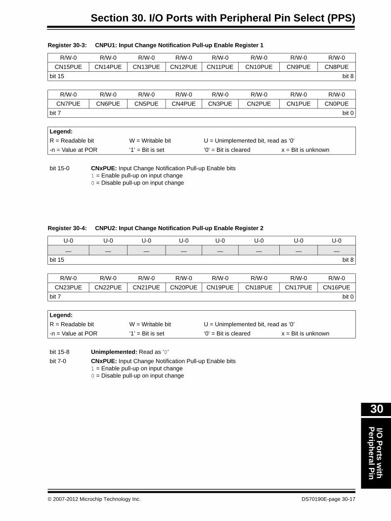
Register 30-3: CNPU1: Input Change Notification Pull-up Enable Register 1
R/W-0 R/W-0 R/W-0 R/W-0 R/W-0 R/W-0 R/W-0 R/W-0CN15PUE CN14PUE CN13PUE CN12PUE CN11PUE CN10PUE CN9PUE CN8PUE
bit 15 bit 8
R/W-0 R/W-0 R/W-0 R/W-0 R/W-0 R/W-0 R/W-0 R/W-0CN7PUE CN6PUE CN5PUE CN4PUE CN3PUE CN2PUE CN1PUE CN0PUE
bit 7 bit 0
Legend:R = Readable bit W = Writable bit U = Unimplemented bit, read as ‘0’-n = Value at POR ‘1’ = Bit is set ‘0’ = Bit is cleared x = Bit is unknown
bit 15-0 CNxPUE: Input Change Notification Pull-up Enable bits1 = Enable pull-up on input change0 = Disable pull-up on input change
Register 30-4: CNPU2: Input Change Notification Pull-up Enable Register 2
U-0 U-0 U-0 U-0 U-0 U-0 U-0 U-0
— — — — — — — —bit 15 bit 8
R/W-0 R/W-0 R/W-0 R/W-0 R/W-0 R/W-0 R/W-0 R/W-0CN23PUE CN22PUE CN21PUE CN20PUE CN19PUE CN18PUE CN17PUE CN16PUE
bit 7 bit 0
Legend:R = Readable bit W = Writable bit U = Unimplemented bit, read as ‘0’-n = Value at POR ‘1’ = Bit is set ‘0’ = Bit is cleared x = Bit is unknown
bit 15-8 Unimplemented: Read as ‘0’bit 7-0 CNxPUE: Input Change Notification Pull-up Enable bits
1 = Enable pull-up on input change0 = Disable pull-up on input change
© 2007-2012 Microchip Technology Inc. DS70190E-page 30-17

dsPIC33F/PIC24H Family Reference Manual
Register 30-5: RPINR0: Peripheral Pin Select Input Register 0
U-0 U-0 U-0 R/W-1 R/W-1 R/W-1 R/W-1 R/W-1— — — INT1R<4:0>
bit 15 bit 8
U-0 U-0 U-0 U-0 U-0 U-0 U-0 U-0— — — — — — — —
bit 7 bit 0
Legend:R = Readable bit W = Writable bit U = Unimplemented bit, read as ‘0’-n = Value at POR ‘1’ = Bit is set ‘0’ = Bit is cleared x = Bit is unknown
bit 15-13 Unimplemented: Read as ‘0’ bit 12-8 INT1R<4:0>: Assign External Interrupt 1 (INTR1) to the Corresponding RPn Pin bits
11111 = Input tied VSS11110 = Input tied to RP30...00001 = Input tied to RP100000 = Input tied to RP0
bit 7-0 Unimplemented: Read as ‘0’
Register 30-6: RPINR1: Peripheral Pin Select Input Register 1
U-0 U-0 U-0 U-0 U-0 U-0 U-0 U-0— — — — — — — —
bit 15 bit 8
U-0 U-0 U-0 R/W-1 R/W-1 R/W-1 R/W-1 R/W-1— — — INT2R<4:0>
bit 7 bit 0
Legend:R = Readable bit W = Writable bit U = Unimplemented bit, read as ‘0’-n = Value at POR ‘1’ = Bit is set ‘0’ = Bit is cleared x = Bit is unknown
bit 15-5 Unimplemented: Read as ‘0’ bit 4-0 INT2R<4:0>: Assign External Interrupt 2 (INTR2) to the Corresponding RPn Pin bits
11111 = Input tied VSS11110 = Input tied to RP30...00001 = Input tied to RP100000 = Input tied to RP0
DS70190E-page 30-18 © 2007-2012 Microchip Technology Inc.

Section 30. I/O Ports with Peripheral Pin Select (PPS)I/O
Ports with
Peripheral Pin
30
Register 30-7: RPINR3: Peripheral Pin Select Input Register 3
U-0 U-0 U-0 R/W-1 R/W-1 R/W-1 R/W-1 R/W-1— — — T3CKR<4:0>
bit 15 bit 8
U-0 U-0 U-0 R/W-1 R/W-1 R/W-1 R/W-1 R/W-1— — — T2CKR<4:0>
bit 7 bit 0
Legend:R = Readable bit W = Writable bit U = Unimplemented bit, read as ‘0’-n = Value at POR ‘1’ = Bit is set ‘0’ = Bit is cleared x = Bit is unknown
bit 15-13 Unimplemented: Read as ‘0’ bit 12-8 T3CKR<4:0>: Assign Timer3 External Clock (T3CK) to the Corresponding RPn pin
11111 = Input tied VSS11110 = Input tied to RP30...00001 = Input tied to RP100000 = Input tied to RP0
bit 7-5 Unimplemented: Read as ‘0’ bit 4-0 T2CKR<4:0>: Assign Timer2 External Clock (T2CK) to the Corresponding RPn pin
11111 = Input tied VSS11110 = Input tied to RP30...00001 = Input tied to RP100000 = Input tied to RP0
© 2007-2012 Microchip Technology Inc. DS70190E-page 30-19

dsPIC33F/PIC24H Family Reference Manual
Register 30-8: RPINR7: Peripheral Pin Select Input Register 7
U-0 U-0 U-0 R/W-1 R/W-1 R/W-1 R/W-1 R/W-1— — — IC2R<4:0>
bit 15 bit 8
U-0 U-0 U-0 R/W-1 R/W-1 R/W-1 R/W-1 R/W-1— — — IC1R<4:0>
bit 7 bit 0
Legend:R = Readable bit W = Writable bit U = Unimplemented bit, read as ‘0’-n = Value at POR ‘1’ = Bit is set ‘0’ = Bit is cleared x = Bit is unknown
bit 15-13 Unimplemented: Read as ‘0’ bit 12-8 IC2R<4:0>: Assign Input Capture 2 (IC2) to the Corresponding RPn Pin bits
11111 = Input tied VSS11110 = Input tied to RP30...00001 = Input tied to RP100000 = Input tied to RP0
bit 7-5 Unimplemented: Read as ‘0’ bit 4-0 IC1R<4:0>: Assign Input Capture 1 (IC1) to the Corresponding RPn Pin bits
11111 = Input tied VSS11110 = Input tied to RP30...00001 = Input tied to RP100000 = Input tied to RP0
DS70190E-page 30-20 © 2007-2012 Microchip Technology Inc.
Section 30. I/O Ports with Peripheral Pin Select (PPS)I/O
Ports with
Peripheral Pin
30
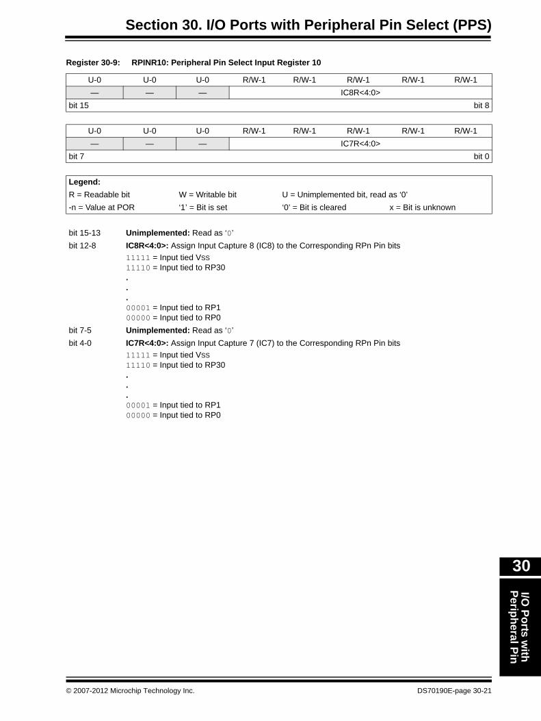
Register 30-9: RPINR10: Peripheral Pin Select Input Register 10
U-0 U-0 U-0 R/W-1 R/W-1 R/W-1 R/W-1 R/W-1— — — IC8R<4:0>
bit 15 bit 8
U-0 U-0 U-0 R/W-1 R/W-1 R/W-1 R/W-1 R/W-1— — — IC7R<4:0>
bit 7 bit 0
Legend:R = Readable bit W = Writable bit U = Unimplemented bit, read as ‘0’-n = Value at POR ‘1’ = Bit is set ‘0’ = Bit is cleared x = Bit is unknown
bit 15-13 Unimplemented: Read as ‘0’ bit 12-8 IC8R<4:0>: Assign Input Capture 8 (IC8) to the Corresponding RPn Pin bits
11111 = Input tied VSS11110 = Input tied to RP30...00001 = Input tied to RP100000 = Input tied to RP0
bit 7-5 Unimplemented: Read as ‘0’ bit 4-0 IC7R<4:0>: Assign Input Capture 7 (IC7) to the Corresponding RPn Pin bits
11111 = Input tied VSS11110 = Input tied to RP30...00001 = Input tied to RP100000 = Input tied to RP0
© 2007-2012 Microchip Technology Inc. DS70190E-page 30-21

dsPIC33F/PIC24H Family Reference Manual
Register 30-10: RPINR11: Peripheral Pin Select Input Register 11
U-0 U-0 U-0 U-0 U-0 U-0 U-0 U-0— — — — — — — —
bit 15 bit 8
U-0 U-0 U-0 R/W-1 R/W-1 R/W-1 R/W-1 R/W-1— — — OCFAR<4:0>
bit 7 bit 0
Legend:R = Readable bit W = Writable bit U = Unimplemented bit, read as ‘0’-n = Value at POR ‘1’ = Bit is set ‘0’ = Bit is cleared x = Bit is unknown
bit 15-5 Unimplemented: Read as ‘0’ bit 4-0 OCFAR<4:0>: Assign Output Capture A (OCFA) to the Corresponding RPn Pin bits
11111 = Input tied VSS11110 = Input tied to RP30...00001 = Input tied to RP100000 = Input tied to RP0
Register 30-11: RPINR12: Peripheral Pin Select Input Register 12
U-0 U-0 U-0 U-0 U-0 U-0 U-0 U-0— — — — — — — —
bit 15 bit 8
U-0 U-0 U-0 R/W-1 R/W-1 R/W-1 R/W-1 R/W-1— — — FLTA1R<4:0>
bit 7 bit 0
Legend:R = Readable bit W = Writable bit U = Unimplemented bit, read as ‘0’-n = Value at POR ‘1’ = Bit is set ‘0’ = Bit is cleared x = Bit is unknown
bit 15-5 Unimplemented: Read as ‘0’ bit 4-0 FLTA1R<4:0>: Assign PWM1 Fault (FLTA1) to the Corresponding RPn Pin bits
11111 = Input tied VSS11110 = Input tied to RP30...00001 = Input tied to RP100000 = Input tied to RP0
DS70190E-page 30-22 © 2007-2012 Microchip Technology Inc.

Section 30. I/O Ports with Peripheral Pin Select (PPS)I/O
Ports with
Peripheral Pin
30
Register 30-12: RPINR13: Peripheral Pin Select Input Register 13
U-0 U-0 U-0 U-0 U-0 U-0 U-0 U-0— — — — — — — —
bit 15 bit 8
U-0 U-0 U-0 R/W-1 R/W-1 R/W-1 R/W-1 R/W-1— — — FLTA2R<4:0>
bit 7 bit 0
Legend:R = Readable bit W = Writable bit U = Unimplemented bit, read as ‘0’-n = Value at POR ‘1’ = Bit is set ‘0’ = Bit is cleared x = Bit is unknown
bit 15-5 Unimplemented: Read as ‘0’ bit 4-0 FLTA2R<4:0>: Assign PWM2 Fault (FLTA2) to the Corresponding RPn Pin bits
11111 = Input tied VSS11110 = Input tied to RP30...00001 = Input tied to RP100000 = Input tied to RP0
© 2007-2012 Microchip Technology Inc. DS70190E-page 30-23

dsPIC33F/PIC24H Family Reference Manual
Register 30-13: RPINR14: Peripheral Pin Select Input Register 14
U-0 U-0 U-0 R/W-1 R/W-1 R/W-1 R/W-1 R/W-1— — — QEBR<4:0>
bit 15 bit 8
U-0 U-0 U-0 R/W-1 R/W-1 R/W-1 R/W-1 R/W-1— — — QEAR<4:0>
bit 7 bit 0
Legend:R = Readable bit W = Writable bit U = Unimplemented bit, read as ‘0’-n = Value at POR ‘1’ = Bit is set ‘0’ = Bit is cleared x = Bit is unknown
bit 15-13 Unimplemented: Read as ‘0’ bit 12-8 QEBR<4:0>: Assign B (QEB) to the Corresponding RPn Pin bits
11111 = Input tied VSS11110 = Input tied to RP30...00001 = Input tied to RP100000 = Input tied to RP0
bit 7-5 Unimplemented: Read as ‘0’ bit 4-0 QEAR<4:0>: Assign A (QEA) to the Corresponding RPn Pin bits
11111 = Input tied VSS11110 = Input tied to RP30...00001 = Input tied to RP100000 = Input tied to RP0
DS70190E-page 30-24 © 2007-2012 Microchip Technology Inc.
Section 30. I/O Ports with Peripheral Pin Select (PPS)I/O
Ports with
Peripheral Pin
30
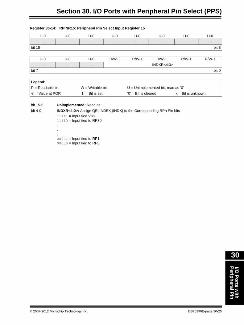
Register 30-14: RPINR15: Peripheral Pin Select Input Register 15
U-0 U-0 U-0 U-0 U-0 U-0 U-0 U-0— — — — — — — —
bit 15 bit 8
U-0 U-0 U-0 R/W-1 R/W-1 R/W-1 R/W-1 R/W-1— — — INDXR<4:0>
bit 7 bit 0
Legend:R = Readable bit W = Writable bit U = Unimplemented bit, read as ‘0’-n = Value at POR ‘1’ = Bit is set ‘0’ = Bit is cleared x = Bit is unknown
bit 15-5 Unimplemented: Read as ‘0’ bit 4-0 INDXR<4:0>: Assign QEI INDEX (INDX) to the Corresponding RPn Pin bits
11111 = Input tied VSS11110 = Input tied to RP30...00001 = Input tied to RP100000 = Input tied to RP0
© 2007-2012 Microchip Technology Inc. DS70190E-page 30-25
dsPIC33F/PIC24H Family Reference Manual
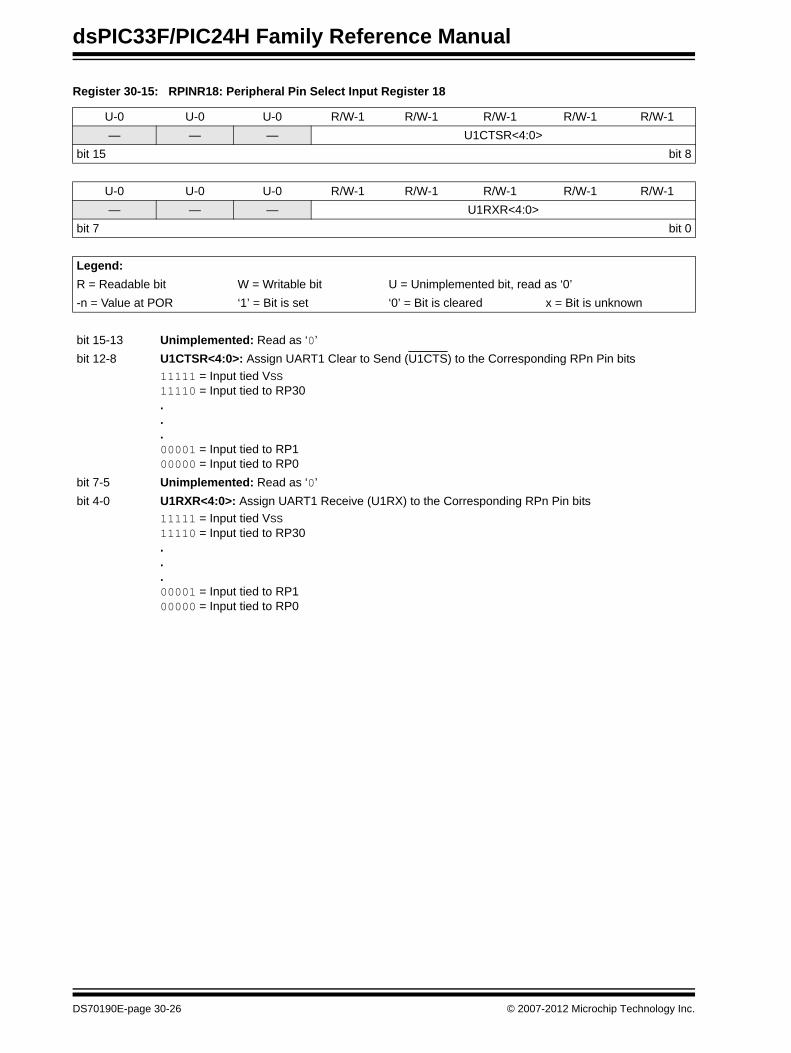
Register 30-15: RPINR18: Peripheral Pin Select Input Register 18
U-0 U-0 U-0 R/W-1 R/W-1 R/W-1 R/W-1 R/W-1— — — U1CTSR<4:0>
bit 15 bit 8
U-0 U-0 U-0 R/W-1 R/W-1 R/W-1 R/W-1 R/W-1— — — U1RXR<4:0>
bit 7 bit 0
Legend:R = Readable bit W = Writable bit U = Unimplemented bit, read as ‘0’-n = Value at POR ‘1’ = Bit is set ‘0’ = Bit is cleared x = Bit is unknown
bit 15-13 Unimplemented: Read as ‘0’ bit 12-8 U1CTSR<4:0>: Assign UART1 Clear to Send (U1CTS) to the Corresponding RPn Pin bits
11111 = Input tied VSS11110 = Input tied to RP30...00001 = Input tied to RP100000 = Input tied to RP0
bit 7-5 Unimplemented: Read as ‘0’ bit 4-0 U1RXR<4:0>: Assign UART1 Receive (U1RX) to the Corresponding RPn Pin bits
11111 = Input tied VSS11110 = Input tied to RP30...00001 = Input tied to RP100000 = Input tied to RP0
DS70190E-page 30-26 © 2007-2012 Microchip Technology Inc.

Section 30. I/O Ports with Peripheral Pin Select (PPS)I/O
Ports with
Peripheral Pin
30
Register 30-16: RPINR20: Peripheral Pin Select Input Register 20
U-0 U-0 U-0 R/W-1 R/W-1 R/W-1 R/W-1 R/W-1— — — SCK1R<4:0>
bit 15 bit 8
U-0 U-0 U-0 R/W-1 R/W-1 R/W-1 R/W-1 R/W-1— — — SDI1R<4:0>
bit 7 bit 0
Legend:R = Readable bit W = Writable bit U = Unimplemented bit, read as ‘0’-n = Value at POR ‘1’ = Bit is set ‘0’ = Bit is cleared x = Bit is unknown
bit 15-13 Unimplemented: Read as ‘0’ bit 12-8 SCK1R<4:0>: Assign SPI1 Clock Input (SCK1IN) to the Corresponding RPn Pin bits
11111 = Input tied VSS11110 = Input tied to RP30...00001 = Input tied to RP100000 = Input tied to RP0
bit 7-5 Unimplemented: Read as ‘0’ bit 4-0 SDI1R<4:0>: Assign SPI1 Data Input (SDI1) to the Corresponding RPn Pin bits
11111 = Input tied VSS11110 = Input tied to RP30...00001 = Input tied to RP100000 = Input tied to RP0
© 2007-2012 Microchip Technology Inc. DS70190E-page 30-27

dsPIC33F/PIC24H Family Reference Manual
Register 30-17: RPINR21: Peripheral Pin Select Input Register 21
U-0 U-0 U-0 U-0 U-0 U-0 U-0 U-0— — — — — — — —
bit 15 bit 8
U-0 U-0 U-0 R/W-1 R/W-1 R/W-1 R/W-1 R/W-1— — — SS1R<4:0>
bit 7 bit 0
Legend:R = Readable bit W = Writable bit U = Unimplemented bit, read as ‘0’-n = Value at POR ‘1’ = Bit is set ‘0’ = Bit is cleared x = Bit is unknown
bit 15-5 Unimplemented: Read as ‘0’ bit 4-0 SS1R<4:0>: Assign SPI1 Slave Select Input (SS1IN) to the Corresponding RPn Pin bits
11111 = Input tied VSS11110 = Input tied to RP30...00001 = Input tied to RP100000 = Input tied to RP0
DS70190E-page 30-28 © 2007-2012 Microchip Technology Inc.
Section 30. I/O Ports with Peripheral Pin Select (PPS)I/O
Ports with
Peripheral Pin
30
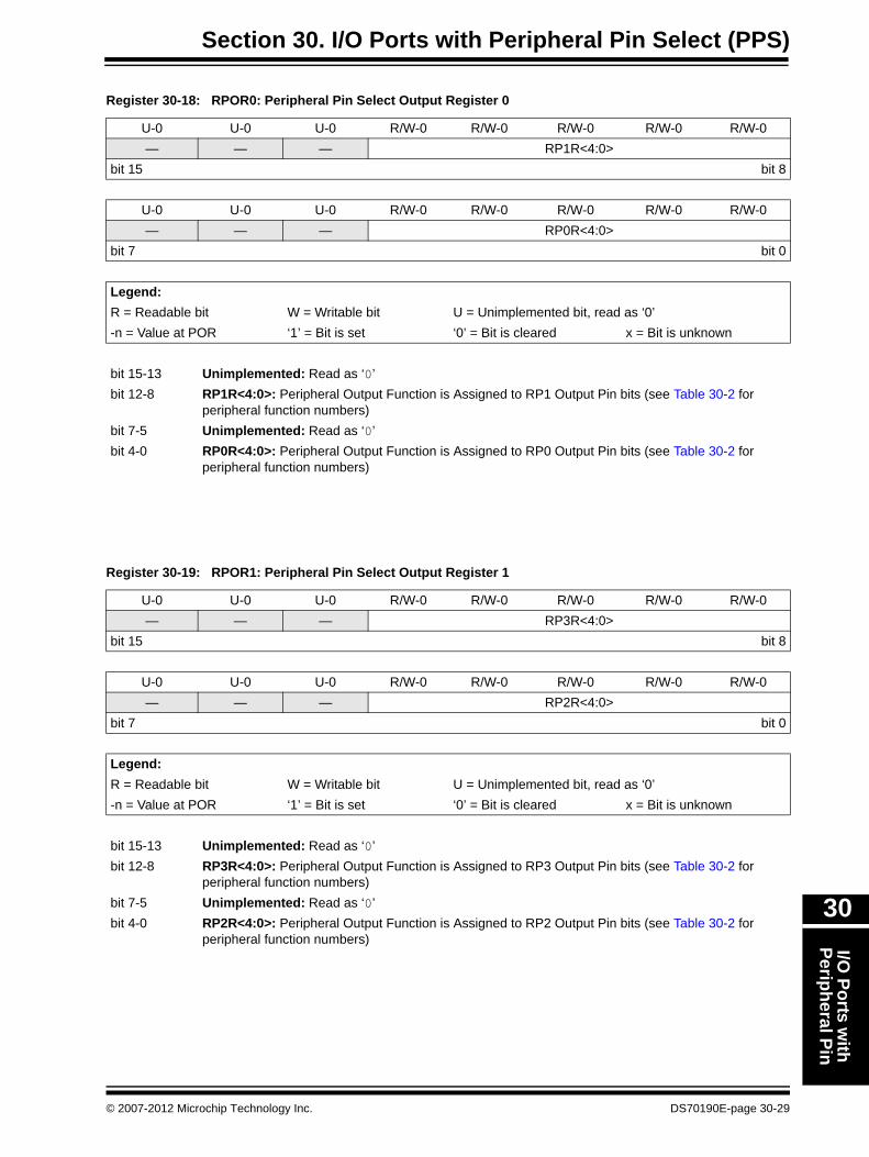
Register 30-18: RPOR0: Peripheral Pin Select Output Register 0
U-0 U-0 U-0 R/W-0 R/W-0 R/W-0 R/W-0 R/W-0— — — RP1R<4:0>
bit 15 bit 8
U-0 U-0 U-0 R/W-0 R/W-0 R/W-0 R/W-0 R/W-0— — — RP0R<4:0>
bit 7 bit 0
Legend:R = Readable bit W = Writable bit U = Unimplemented bit, read as ‘0’-n = Value at POR ‘1’ = Bit is set ‘0’ = Bit is cleared x = Bit is unknown
bit 15-13 Unimplemented: Read as ‘0’ bit 12-8 RP1R<4:0>: Peripheral Output Function is Assigned to RP1 Output Pin bits (see Table 30-2 for
peripheral function numbers)bit 7-5 Unimplemented: Read as ‘0’ bit 4-0 RP0R<4:0>: Peripheral Output Function is Assigned to RP0 Output Pin bits (see Table 30-2 for
peripheral function numbers)
Register 30-19: RPOR1: Peripheral Pin Select Output Register 1
U-0 U-0 U-0 R/W-0 R/W-0 R/W-0 R/W-0 R/W-0— — — RP3R<4:0>
bit 15 bit 8
U-0 U-0 U-0 R/W-0 R/W-0 R/W-0 R/W-0 R/W-0— — — RP2R<4:0>
bit 7 bit 0
Legend:R = Readable bit W = Writable bit U = Unimplemented bit, read as ‘0’-n = Value at POR ‘1’ = Bit is set ‘0’ = Bit is cleared x = Bit is unknown
bit 15-13 Unimplemented: Read as ‘0’ bit 12-8 RP3R<4:0>: Peripheral Output Function is Assigned to RP3 Output Pin bits (see Table 30-2 for
peripheral function numbers)bit 7-5 Unimplemented: Read as ‘0’ bit 4-0 RP2R<4:0>: Peripheral Output Function is Assigned to RP2 Output Pin bits (see Table 30-2 for
peripheral function numbers)
© 2007-2012 Microchip Technology Inc. DS70190E-page 30-29
dsPIC33F/PIC24H Family Reference Manual
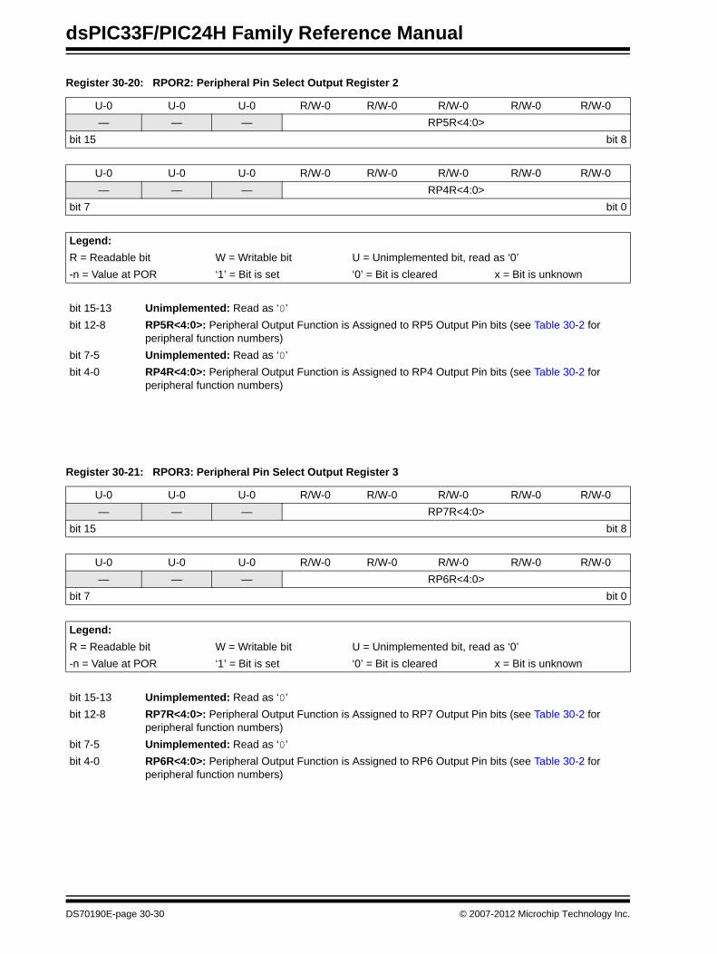
Register 30-20: RPOR2: Peripheral Pin Select Output Register 2
U-0 U-0 U-0 R/W-0 R/W-0 R/W-0 R/W-0 R/W-0— — — RP5R<4:0>
bit 15 bit 8
U-0 U-0 U-0 R/W-0 R/W-0 R/W-0 R/W-0 R/W-0— — — RP4R<4:0>
bit 7 bit 0
Legend:R = Readable bit W = Writable bit U = Unimplemented bit, read as ‘0’-n = Value at POR ‘1’ = Bit is set ‘0’ = Bit is cleared x = Bit is unknown
bit 15-13 Unimplemented: Read as ‘0’ bit 12-8 RP5R<4:0>: Peripheral Output Function is Assigned to RP5 Output Pin bits (see Table 30-2 for
peripheral function numbers)bit 7-5 Unimplemented: Read as ‘0’ bit 4-0 RP4R<4:0>: Peripheral Output Function is Assigned to RP4 Output Pin bits (see Table 30-2 for
peripheral function numbers)
Register 30-21: RPOR3: Peripheral Pin Select Output Register 3
U-0 U-0 U-0 R/W-0 R/W-0 R/W-0 R/W-0 R/W-0— — — RP7R<4:0>
bit 15 bit 8
U-0 U-0 U-0 R/W-0 R/W-0 R/W-0 R/W-0 R/W-0— — — RP6R<4:0>
bit 7 bit 0
Legend:R = Readable bit W = Writable bit U = Unimplemented bit, read as ‘0’-n = Value at POR ‘1’ = Bit is set ‘0’ = Bit is cleared x = Bit is unknown
bit 15-13 Unimplemented: Read as ‘0’ bit 12-8 RP7R<4:0>: Peripheral Output Function is Assigned to RP7 Output Pin bits (see Table 30-2 for
peripheral function numbers)bit 7-5 Unimplemented: Read as ‘0’ bit 4-0 RP6R<4:0>: Peripheral Output Function is Assigned to RP6 Output Pin bits (see Table 30-2 for
peripheral function numbers)
DS70190E-page 30-30 © 2007-2012 Microchip Technology Inc.
Section 30. I/O Ports with Peripheral Pin Select (PPS)I/O
Ports with
Peripheral Pin
30
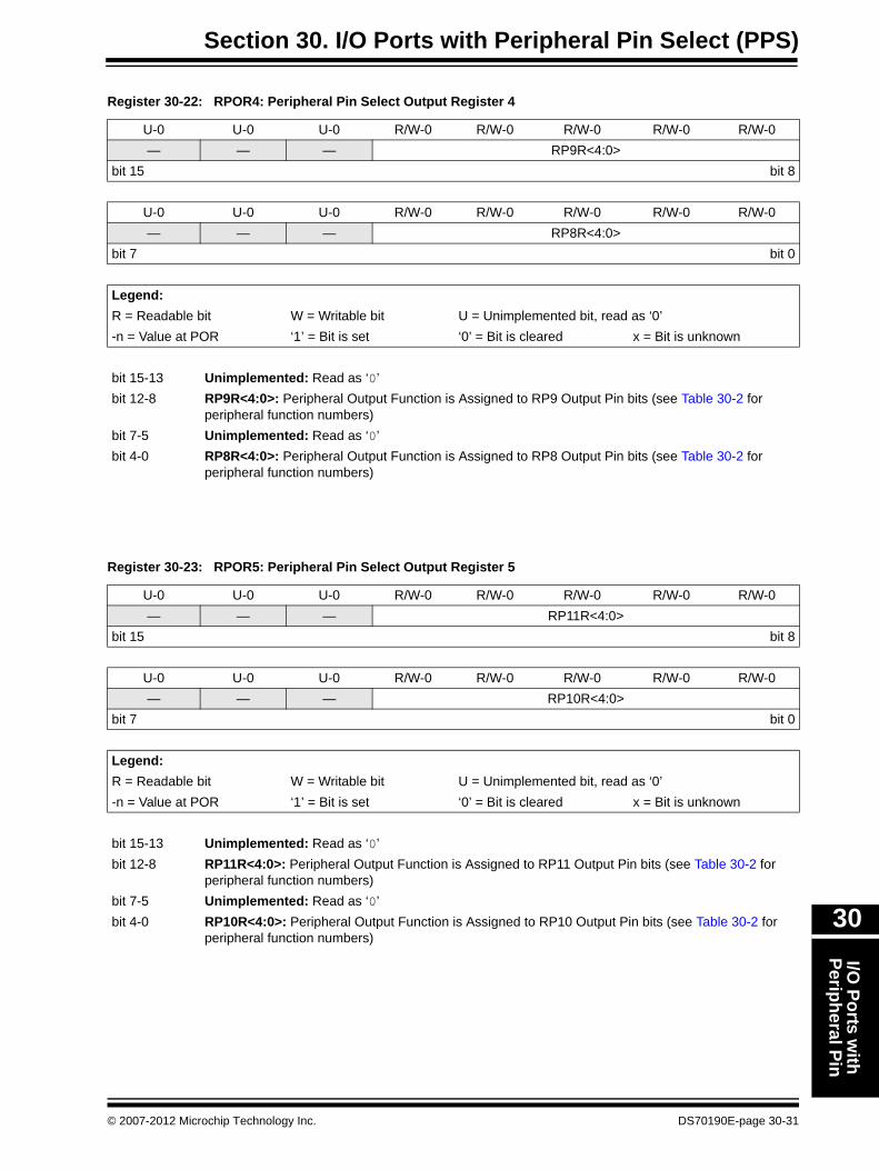
Register 30-22: RPOR4: Peripheral Pin Select Output Register 4
U-0 U-0 U-0 R/W-0 R/W-0 R/W-0 R/W-0 R/W-0— — — RP9R<4:0>
bit 15 bit 8
U-0 U-0 U-0 R/W-0 R/W-0 R/W-0 R/W-0 R/W-0— — — RP8R<4:0>
bit 7 bit 0
Legend:R = Readable bit W = Writable bit U = Unimplemented bit, read as ‘0’-n = Value at POR ‘1’ = Bit is set ‘0’ = Bit is cleared x = Bit is unknown
bit 15-13 Unimplemented: Read as ‘0’ bit 12-8 RP9R<4:0>: Peripheral Output Function is Assigned to RP9 Output Pin bits (see Table 30-2 for
peripheral function numbers)bit 7-5 Unimplemented: Read as ‘0’ bit 4-0 RP8R<4:0>: Peripheral Output Function is Assigned to RP8 Output Pin bits (see Table 30-2 for
peripheral function numbers)
Register 30-23: RPOR5: Peripheral Pin Select Output Register 5
U-0 U-0 U-0 R/W-0 R/W-0 R/W-0 R/W-0 R/W-0— — — RP11R<4:0>
bit 15 bit 8
U-0 U-0 U-0 R/W-0 R/W-0 R/W-0 R/W-0 R/W-0— — — RP10R<4:0>
bit 7 bit 0
Legend:R = Readable bit W = Writable bit U = Unimplemented bit, read as ‘0’-n = Value at POR ‘1’ = Bit is set ‘0’ = Bit is cleared x = Bit is unknown
bit 15-13 Unimplemented: Read as ‘0’ bit 12-8 RP11R<4:0>: Peripheral Output Function is Assigned to RP11 Output Pin bits (see Table 30-2 for
peripheral function numbers)bit 7-5 Unimplemented: Read as ‘0’ bit 4-0 RP10R<4:0>: Peripheral Output Function is Assigned to RP10 Output Pin bits (see Table 30-2 for
peripheral function numbers)
© 2007-2012 Microchip Technology Inc. DS70190E-page 30-31

dsPIC33F/PIC24H Family Reference Manual
Register 30-24: RPOR6: Peripheral Pin Select Output Register 6
U-0 U-0 U-0 R/W-0 R/W-0 R/W-0 R/W-0 R/W-0— — — RP13R<4:0>
bit 15 bit 8
U-0 U-0 U-0 R/W-0 R/W-0 R/W-0 R/W-0 R/W-0— — — RP12R<4:0>
bit 7 bit 0
Legend:R = Readable bit W = Writable bit U = Unimplemented bit, read as ‘0’-n = Value at POR ‘1’ = Bit is set ‘0’ = Bit is cleared x = Bit is unknown
bit 15-13 Unimplemented: Read as ‘0’ bit 12-8 RP13R<4:0>: Peripheral Output Function is Assigned to RP13 Output Pin bits (see Table 30-2 for
peripheral function numbers)bit 7-5 Unimplemented: Read as ‘0’ bit 4-0 RP12R<4:0>: Peripheral Output Function is Assigned to RP12 Output Pin bits (see Table 30-2 for
peripheral function numbers)
Register 30-25: RPOR7: Peripheral Pin Select Output Register 7
U-0 U-0 U-0 R/W-0 R/W-0 R/W-0 R/W-0 R/W-0— — — RP15R<4:0>
bit 15 bit 8
U-0 U-0 U-0 R/W-0 R/W-0 R/W-0 R/W-0 R/W-0— — — RP14R<4:0>
bit 7 bit 0
Legend:R = Readable bit W = Writable bit U = Unimplemented bit, read as ‘0’-n = Value at POR ‘1’ = Bit is set ‘0’ = Bit is cleared x = Bit is unknown
bit 15-13 Unimplemented: Read as ‘0’ bit 12-8 RP15R<4:0>: Peripheral Output Function is Assigned to RP15 Output Pin bits (see Table 30-2 for
peripheral function numbers)bit 7-5 Unimplemented: Read as ‘0’ bit 4-0 RP14R<4:0>: Peripheral Output Function is Assigned to RP14 Output Pin bits (see Table 30-2 for
peripheral function numbers)
Note: Some dsPIC33F/PIC24H devices may have additional RPORx (Peripheral Pin Select Output) registers. For more information, refer to the “I/O Ports with Peripheral Pin Select (PPS)” chapter in the specific device data sheet.
DS70190E-page 30-32 © 2007-2012 Microchip Technology Inc.
Section 30. I/O Ports with Peripheral Pin Select (PPS)I/O
Ports with
Peripheral Pin
30
30.8 DESIGN TIPS
Question 1: Are there situations where an input pin can be safely driven beyond its maximum rating?
Answer: In some cases, certain pins as defined in the I/O Pin Input Specifications table in the “Electrical Characteristics” chapter of the specific device data sheet under “Injection Current”, have internal protection diodes to VDD and VSS. The term “Injection Current” is also referred to as “Clamp Current”. On designated pins, with sufficient external current limiting precautions by the user, I/O pin input voltages are allowed to be greater or less than the data sheet absolute maximum ratings with respect to the VSS and VDD supplies. Note that when the user application forward biases either of the high or low side internal input clamp diodes, that the resulting current being injected into the device that is clamped internally by the VDD and VSS power rails, may affect the ADC accuracy by four to six counts.
Question 2: How are shared pins handled?Answer: I/O pins that are shared with any analog input pin, (i.e., ANx, see the Pinout I/O
Descriptions table in the “Device Overview” chapter in the specific device data sheet), are always analog pins by default after any reset. Consequently, configuring a pin as an analog input pin, automatically disables the digital input pin buffer and any attempt to read the digital input level by reading PORTx or LATx will always return a ‘0’ regardless of the digital logic level on the pin. To use a pin as a digital I/O pin on a shared Analog pin, the user application needs to configure the analog pin configuration registers in the I/O Ports module, (i.e., ANSELx), by setting the appropriate bit that corresponds to that I/O port pin to a ‘0’.
Question 3: How do I determine the priorities of pin functions?Answer: Most I/O pins have multiple functions. Referring to the “Pin Diagrams” in the
specific device data sheet, the priorities of the functions allocated to any pins are indicated by reading the pin name from left-to-right. The left most function name takes precedence over any function to its right in the naming convention. For example: AN16/T2CK/T7CK/RC1. This indicates that AN16 is the highest priority in this example and will supersede all other functions to its right in the list. Those other functions to its right, even if enabled, would not work as long as any other function to its left was enabled. This rule applies to all of the functions listed for a given pin. Dedicated peripheral functions are always higher priority than remappable functions. I/O is always lowest priority.
Question 4: Are external resistors always needed?Answer: Each pin has an internal weak pull-up resistor and pull-down resistor that can be
configured using the CNPUx and CNPDx registers, respectively. These resistors eliminate the need for external resistors in certain applications. The internal pull-up is up to ~(VDD-0.8), not VDD. This value is still above the minimum VIH of CMOS and TTL devices.
Note: Although it is not possible to use a digital input pin when its analog function is enabled, it is possible to use the digital I/O output function, TRISx = 0x0, while the analog function is also enabled. However, this is not recommended, particularly if the analog input is connected to an external analog voltage source, which would create signal contention between the analog signal and the output pin driver.
© 2007-2012 Microchip Technology Inc. DS70190E-page 30-33

dsPIC33F/PIC24H Family Reference Manual
Question 5: Are there any design considerations I should be aware of when driving LEDs?
Answer: When driving LEDs directly, the I/O pin can source or sink more current than what is specified in the VOH/IOH and VOL/IOL DC characteristic specification. The respective IOH and IOL current rating only applies to maintaining the corresponding output at or above the VOH and at or below the VOL levels. However, for LEDs unlike digital inputs of an externally connected device, they are not governed by the same minimum VIH/VIL levels. An I/O pin output can safely sink or source any current less than that listed in the absolute maximum rating section of the data sheet. For example:
VOH = 2.4v @ IOH = -8 mA and VDD = 3.3V
The maximum output current sourced by any 8 mA I/O pin = 12 mA. LED source current < 12 mA is technically permitted. Refer to the VOH/IOH specifications in the “Electrical Characteristics” chapter of the specific device data sheet for additional information.
Question 6: What are the PPS pin mapping rules?Answer: The Peripheral Pin Select (PPS) pin mapping rules are as follows:
1. Only one “output” function can be active on a given pin at any time regardless if it is a dedicated or remappable function (one pin, one output).
2. It is possible to assign a “remappable output” function to multiple pins and externally short or tie them together for increased current drive.
3. If any “dedicated output” function is enabled on a pin it will take precedence over any remappable “output” function.
4. If any “dedicated digital”, (input or output), function is enabled on a pin, any number of “input” remappable functions can be mapped to the same pin.
5. If any “dedicated analog” function(s) are enabled on a given pin, “digital input(s)” of any kind will all be disabled, although a single “digital output” at the user cautionary discretion can be enabled and active as long as there is no signal contention with an external analog input signal. For example it is possible for the ADC to convert the digital output logic level or to toggle a digital output on a comparator or ADC input provided there is no external analog input like for a built-in self test.
6. Any number of “input” remappable functions can be mapped to the same pin(s) at the same time, including to any pin with single output from either a dedicated or remappable “output”.
7. The TRIS registers control only the digital I/O output buffer. Any other dedicated or remappable active “output” will automatically override the TRIS setting. The TRIS register does not control the digital logic “input” buffer. Remappable digital “inputs” do not automatically override TRIS settings which means that the TRIS bit must be set to input for pins with only remappable input function(s) assigned
8. All analog pins are enabled by default after any reset and the corresponding digital input buffer on the pin is disabled. Only the Analog pin select registers control the digital input buffer, not the TRIS register. The user must disable the analog function on a pin using the analog pin select registers in order to use any “digital input(s)” on a corresponding pin, no exceptions.
DS70190E-page 30-34 © 2007-2012 Microchip Technology Inc.
Section 30. I/O Ports with Peripheral Pin Select (PPS)I/O
Ports with
Peripheral Pin
30
30.9 RELATED APPLICATION NOTESThis section lists application notes that are related to this section of the manual. These application notes may not be written specifically for the dsPIC33F/PIC24H Product Family, but the concepts are pertinent and could be used with modification and possible limitations. The current application notes related to I/O Ports with Peripheral Pin Select (PPS) include the following:
Title Application Note #Implementing Wake-up on Key Stroke AN552
Note: Please visit the Microchip web site (www.microchip.com) for additional application notes and code examples for the dsPIC33F/PIC24H family of devices.
© 2007-2012 Microchip Technology Inc. DS70190E-page 30-35

dsPIC33F/PIC24H Family Reference Manual
30.10 REVISION HISTORY
Revision A (February 2007)This is the initial released version of this document.
Revision B (February 2007)Minor edits throughout document.
Revision C (June 2008)This revision includes the following updates:
• Example 30-2: “Configuring UART1 Input and Output Functions” has been updated with entirely new content.
• Additional minor corrections such as language and formatting updates have been incorporated throughout the document.
Revision D (July 2010)This revision includes the following updates:
• Renamed the Family Reference Manual name from dsPIC33F to dsPIC33F/PIC24H• All references to dsPIC33F in the document are updated to dsPIC33F/PIC24H• Notes:
- Added a shaded note at the beginning of the section, which provides information on complementary documentation
• Deleted CN interrupt paragraph from the 30.5.2 “CN Configuration and Operation” section
• Additional minor corrections such as language and formatting updates have been incorporated throughout the document
Revision E (April 2012)This revision includes the following updates
• Added 30.8 “Design Tips”• Additional minor updates to text and formatting were incorporated throughout the document
DS70190E-page 30-36 © 2007-2012 Microchip Technology Inc.

Note the following details of the code protection feature on Microchip devices:• Microchip products meet the specification contained in their particular Microchip Data Sheet.
• Microchip believes that its family of products is one of the most secure families of its kind on the market today, when used in the intended manner and under normal conditions.
• There are dishonest and possibly illegal methods used to breach the code protection feature. All of these methods, to our knowledge, require using the Microchip products in a manner outside the operating specifications contained in Microchip’s Data Sheets. Most likely, the person doing so is engaged in theft of intellectual property.
• Microchip is willing to work with the customer who is concerned about the integrity of their code.
• Neither Microchip nor any other semiconductor manufacturer can guarantee the security of their code. Code protection does not mean that we are guaranteeing the product as “unbreakable.”
Code protection is constantly evolving. We at Microchip are committed to continuously improving the code protection features of our products. Attempts to break Microchip’s code protection feature may be a violation of the Digital Millennium Copyright Act. If such acts allow unauthorized access to your software or other copyrighted work, you may have a right to sue for relief under that Act.
Information contained in this publication regarding device applications and the like is provided only for your convenience and may be superseded by updates. It is your responsibility to ensure that your application meets with your specifications. MICROCHIP MAKES NO REPRESENTATIONS OR WARRANTIES OF ANY KIND WHETHER EXPRESS OR IMPLIED, WRITTEN OR ORAL, STATUTORY OR OTHERWISE, RELATED TO THE INFORMATION, INCLUDING BUT NOT LIMITED TO ITS CONDITION, QUALITY, PERFORMANCE, MERCHANTABILITY OR FITNESS FOR PURPOSE. Microchip disclaims all liability arising from this information and its use. Use of Microchip devices in life support and/or safety applications is entirely at the buyer’s risk, and the buyer agrees to defend, indemnify and hold harmless Microchip from any and all damages, claims, suits, or expenses resulting from such use. No licenses are conveyed, implicitly or otherwise, under any Microchip intellectual property rights.
© 2007-2012 Microchip Technology Inc.
QUALITY MANAGEMENT SYSTEM CERTIFIED BY DNV
== ISO/TS 16949 ==
Trademarks
The Microchip name and logo, the Microchip logo, dsPIC, KEELOQ, KEELOQ logo, MPLAB, PIC, PICmicro, PICSTART, PIC32 logo, rfPIC and UNI/O are registered trademarks of Microchip Technology Incorporated in the U.S.A. and other countries.
FilterLab, Hampshire, HI-TECH C, Linear Active Thermistor, MXDEV, MXLAB, SEEVAL and The Embedded Control Solutions Company are registered trademarks of Microchip Technology Incorporated in the U.S.A.
Analog-for-the-Digital Age, Application Maestro, chipKIT, chipKIT logo, CodeGuard, dsPICDEM, dsPICDEM.net, dsPICworks, dsSPEAK, ECAN, ECONOMONITOR, FanSense, HI-TIDE, In-Circuit Serial Programming, ICSP, Mindi, MiWi, MPASM, MPLAB Certified logo, MPLIB, MPLINK, mTouch, Omniscient Code Generation, PICC, PICC-18, PICDEM, PICDEM.net, PICkit, PICtail, REAL ICE, rfLAB, Select Mode, Total Endurance, TSHARC, UniWinDriver, WiperLock and ZENA are trademarks of Microchip Technology Incorporated in the U.S.A. and other countries.
SQTP is a service mark of Microchip Technology Incorporated in the U.S.A.
All other trademarks mentioned herein are property of their respective companies.
© 2007-2012, Microchip Technology Incorporated, Printed in the U.S.A., All Rights Reserved.
Printed on recycled paper.
ISBN: 978-1-62076-226-4
DS70190E-page 30 -37
Microchip received ISO/TS-16949:2009 certification for its worldwide headquarters, design and wafer fabrication facilities in Chandler and Tempe, Arizona; Gresham, Oregon and design centers in California and India. The Company’s quality system processes and procedures are for its PIC® MCUs and dsPIC® DSCs, KEELOQ® code hopping devices, Serial EEPROMs, microperipherals, nonvolatile memory and analog products. In addition, Microchip’s quality system for the design and manufacture of development systems is ISO 9001:2000 certified.

DS70190E-page 30 -38 © 2007-2012 Microchip Technology Inc.
AMERICASCorporate Office2355 West Chandler Blvd.Chandler, AZ 85224-6199Tel: 480-792-7200 Fax: 480-792-7277Technical Support: http://www.microchip.com/supportWeb Address: www.microchip.comAtlantaDuluth, GA Tel: 678-957-9614 Fax: 678-957-1455BostonWestborough, MA Tel: 774-760-0087 Fax: 774-760-0088ChicagoItasca, IL Tel: 630-285-0071 Fax: 630-285-0075ClevelandIndependence, OH Tel: 216-447-0464 Fax: 216-447-0643DallasAddison, TX Tel: 972-818-7423 Fax: 972-818-2924DetroitFarmington Hills, MI Tel: 248-538-2250Fax: 248-538-2260IndianapolisNoblesville, IN Tel: 317-773-8323Fax: 317-773-5453Los AngelesMission Viejo, CA Tel: 949-462-9523 Fax: 949-462-9608Santa ClaraSanta Clara, CA Tel: 408-961-6444Fax: 408-961-6445TorontoMississauga, Ontario, CanadaTel: 905-673-0699 Fax: 905-673-6509
ASIA/PACIFICAsia Pacific OfficeSuites 3707-14, 37th FloorTower 6, The GatewayHarbour City, KowloonHong KongTel: 852-2401-1200Fax: 852-2401-3431Australia - SydneyTel: 61-2-9868-6733Fax: 61-2-9868-6755China - BeijingTel: 86-10-8569-7000 Fax: 86-10-8528-2104China - ChengduTel: 86-28-8665-5511Fax: 86-28-8665-7889China - ChongqingTel: 86-23-8980-9588Fax: 86-23-8980-9500China - HangzhouTel: 86-571-2819-3187 Fax: 86-571-2819-3189China - Hong Kong SARTel: 852-2401-1200 Fax: 852-2401-3431China - NanjingTel: 86-25-8473-2460Fax: 86-25-8473-2470China - QingdaoTel: 86-532-8502-7355Fax: 86-532-8502-7205China - ShanghaiTel: 86-21-5407-5533 Fax: 86-21-5407-5066China - ShenyangTel: 86-24-2334-2829Fax: 86-24-2334-2393China - ShenzhenTel: 86-755-8203-2660 Fax: 86-755-8203-1760China - WuhanTel: 86-27-5980-5300Fax: 86-27-5980-5118China - XianTel: 86-29-8833-7252Fax: 86-29-8833-7256China - XiamenTel: 86-592-2388138 Fax: 86-592-2388130China - ZhuhaiTel: 86-756-3210040 Fax: 86-756-3210049
ASIA/PACIFICIndia - BangaloreTel: 91-80-3090-4444 Fax: 91-80-3090-4123India - New DelhiTel: 91-11-4160-8631Fax: 91-11-4160-8632India - PuneTel: 91-20-2566-1512Fax: 91-20-2566-1513Japan - OsakaTel: 81-66-152-7160 Fax: 81-66-152-9310Japan - YokohamaTel: 81-45-471- 6166 Fax: 81-45-471-6122Korea - DaeguTel: 82-53-744-4301Fax: 82-53-744-4302Korea - SeoulTel: 82-2-554-7200Fax: 82-2-558-5932 or 82-2-558-5934Malaysia - Kuala LumpurTel: 60-3-6201-9857Fax: 60-3-6201-9859Malaysia - PenangTel: 60-4-227-8870Fax: 60-4-227-4068Philippines - ManilaTel: 63-2-634-9065Fax: 63-2-634-9069SingaporeTel: 65-6334-8870Fax: 65-6334-8850Taiwan - Hsin ChuTel: 886-3-5778-366Fax: 886-3-5770-955Taiwan - KaohsiungTel: 886-7-536-4818Fax: 886-7-330-9305Taiwan - TaipeiTel: 886-2-2500-6610 Fax: 886-2-2508-0102Thailand - BangkokTel: 66-2-694-1351Fax: 66-2-694-1350
EUROPEAustria - WelsTel: 43-7242-2244-39Fax: 43-7242-2244-393Denmark - CopenhagenTel: 45-4450-2828 Fax: 45-4485-2829France - ParisTel: 33-1-69-53-63-20 Fax: 33-1-69-30-90-79Germany - MunichTel: 49-89-627-144-0 Fax: 49-89-627-144-44Italy - Milan Tel: 39-0331-742611 Fax: 39-0331-466781Netherlands - DrunenTel: 31-416-690399 Fax: 31-416-690340Spain - MadridTel: 34-91-708-08-90Fax: 34-91-708-08-91UK - WokinghamTel: 44-118-921-5869Fax: 44-118-921-5820
Worldwide Sales and Service
11/29/11