Section 23. CAN Module - dsPIC30F FRMww1.microchip.com/downloads/en/DeviceDoc/70070D.pdf · Section...
74
© 2007 Microchip Technology Inc. DS70070D-page 23-1 CAN Module 23 Section 23. CAN Module HIGHLIGHTS This section of the manual contains the following major topics: 23.1 Introduction .................................................................................................................. 23-2 23.2 Control Registers for the CAN Module......................................................................... 23-2 23.3 Register Maps ............................................................................................................ 23-22 23.4 CAN Module Features ............................................................................................... 23-28 23.5 CAN Module Implementation ..................................................................................... 23-29 23.6 CAN Module Operation Modes .................................................................................. 23-36 23.7 Message Reception ................................................................................................... 23-39 23.8 Transmission.............................................................................................................. 23-49 23.9 Error Detection ........................................................................................................... 23-58 23.10 CAN Baud Rate ......................................................................................................... 23-60 23.11 Interrupts .................................................................................................................... 23-64 23.12 CAN Capture.............................................................................................................. 23-65 23.13 CAN Module I/O......................................................................................................... 23-65 23.14 Operation in CPU Power Saving Modes .................................................................... 23-66 23.15 CAN Protocol Overview ............................................................................................. 23-68 23.16 Related Application Notes.......................................................................................... 23-72 23.17 Revision History ......................................................................................................... 23-73
Transcript of Section 23. CAN Module - dsPIC30F FRMww1.microchip.com/downloads/en/DeviceDoc/70070D.pdf · Section...

Section 23. CAN Module
CA
N M
odule
23
HIGHLIGHTSThis section of the manual contains the following major topics:
23.1 Introduction .................................................................................................................. 23-223.2 Control Registers for the CAN Module......................................................................... 23-223.3 Register Maps............................................................................................................ 23-2223.4 CAN Module Features ............................................................................................... 23-2823.5 CAN Module Implementation ..................................................................................... 23-2923.6 CAN Module Operation Modes .................................................................................. 23-3623.7 Message Reception ................................................................................................... 23-3923.8 Transmission.............................................................................................................. 23-4923.9 Error Detection........................................................................................................... 23-5823.10 CAN Baud Rate ......................................................................................................... 23-6023.11 Interrupts.................................................................................................................... 23-6423.12 CAN Capture.............................................................................................................. 23-6523.13 CAN Module I/O......................................................................................................... 23-6523.14 Operation in CPU Power Saving Modes.................................................................... 23-6623.15 CAN Protocol Overview ............................................................................................. 23-6823.16 Related Application Notes.......................................................................................... 23-7223.17 Revision History ......................................................................................................... 23-73
© 2007 Microchip Technology Inc. DS70070D-page 23-1

dsPIC30F Family Reference Manual
23.1 Introduction The Controller Area Network (CAN) module is a serial interface useful for communicating withother peripherals or microcontroller devices. This interface/protocol was designed to allowcommunications within noisy environments. Figure 23-1 shows an example CAN bus network.
Figure 23-1: CAN Bus Network
23.2 Control Registers for the CAN ModuleThere are many registers associated with the CAN module. Descriptions of these registers aregrouped into the following sections:
• Control and Status Registers• Transmit Buffer Registers• Receive Buffer Registers• Baud Rate Control Registers• Interrupt Status and Control Registers
MCP2510SPI™
Interface
CANBus
dsPIC30Fwith CAN
Microchip
PIC MCUwith integrated
CAN
MCP2551Transceiver
MCP2551Transceiver
MCP2551Transceiver
MCP2551Transceiver
MCP2551Transceiver
dsPIC30Fwith integrated
CAN
dsPIC30Fwith integrated
CANPIC MCU
Note 1: ‘i’ in the register identifier denotes the specific CAN module (CAN1 or CAN2).2: ‘n’ in the register identifier denotes the buffer, filter or mask number.3: ‘m’ in the register identifier denotes the word number within a particular CAN data
field.
DS70070D-page 23-2 © 2007 Microchip Technology Inc.

Section 23. CANC
AN
Module
23
23.2.1 CAN Control and Status Registers
Register 23-1: CiCTRL: CAN Module Control and Status Register Upper Byte:
R/W-x U-0 R/W-0 R/W-0 R/W-0 R/W-1 R/W-0 R/W-0CANCAP — CSIDL ABAT CANCKS REQOP<2:0>
bit 15 bit 8
Lower Byte:R-1 R-0 R-0 U-0 R-0 R-0 R-0 U-0
OPMODE<2:0> — ICODE<2:0> —bit 7 bit 0
bit 15 CANCAP: CAN Message Receive Capture Enable bit1 = Enable CAN capture0 = Disable CAN capture
Note: CANCAP is always writable, regardless of CAN module Operating mode.bit 14 Unimplemented: Read as ‘0’bit 13 CSIDL: Stop in Idle Mode bit
1 = Discontinue CAN module operation when device enters Idle mode0 = Continue CAN module operation in Idle mode
bit 12 ABAT: Abort All Pending Transmissions bit1 = Abort pending transmissions in all Transmit Buffers0 = No effect
Note: Module will clear this bit when all transmissions aborted.bit 11 CANCKS: CAN Master Clock Select bit
1 = FCAN clock is FCY0 = FCAN clock is 4 FCY
bit 10-8 REQOP<2:0>: Request Operation Mode bits111 = Set Listen All Messages mode110 = Reserved101 = Reserved100 = Set Configuration mode 011 = Set Listen Only mode010 = Set Loopback mode001 = Set Disable mode000 = Set Normal Operation mode
bit 7-5 OPMODE<2:0>: Operation Mode bitsNote: These bits indicate the current Operating mode of the CAN module. See description for REQOP
bits (CiCTRL<10:8>).bit 4 Unimplemented: Read as ‘0’
© 2007 Microchip Technology Inc. DS70070D-page 23-3

dsPIC30F Family Reference Manual
Register 23-1: CiCTRL: CAN Module Control and Status Register (Continued)
bit 3-1 ICODE<2:0>: Interrupt Flag Code bits111 = Wake-up interrupt110 = RXB0 interrupt101 = RXB1 interrupt100 = TXB0 interrupt011 = TXB1 interrupt010 = TXB2 interrupt001 = Error interrupt000 = No interrupt
bit 0 Unimplemented: Read as ‘0’
Legend:R = Readable bit W = Writable bit U = Unimplemented bit, read as ‘0’-n = Value at POR ‘1’ = Bit is set ‘0’ = Bit is cleared x = Bit is unknown
DS70070D-page 23-4 © 2007 Microchip Technology Inc.
Section 23. CANC
AN
Module
23
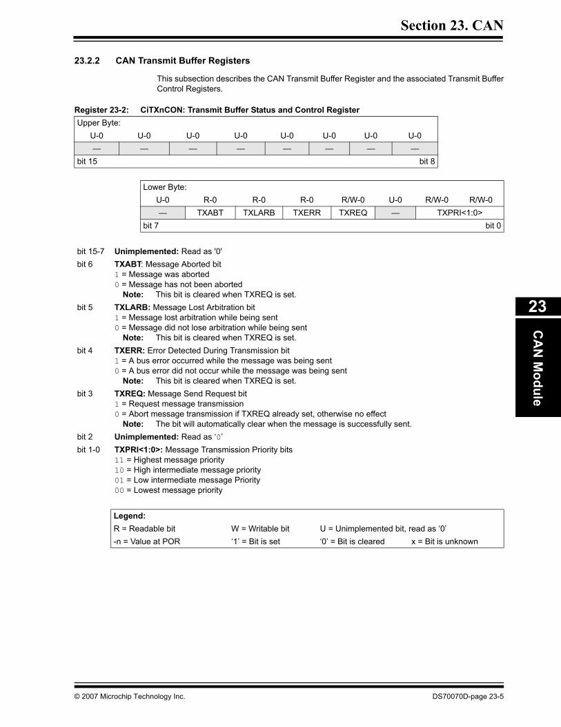
23.2.2 CAN Transmit Buffer Registers
This subsection describes the CAN Transmit Buffer Register and the associated Transmit BufferControl Registers.
Register 23-2: CiTXnCON: Transmit Buffer Status and Control RegisterUpper Byte:
U-0 U-0 U-0 U-0 U-0 U-0 U-0 U-0— — — — — — — —
bit 15 bit 8
Lower Byte:U-0 R-0 R-0 R-0 R/W-0 U-0 R/W-0 R/W-0— TXABT TXLARB TXERR TXREQ — TXPRI<1:0>
bit 7 bit 0
bit 15-7 Unimplemented: Read as '0'bit 6 TXABT: Message Aborted bit
1 = Message was aborted0 = Message has not been aborted
Note: This bit is cleared when TXREQ is set.bit 5 TXLARB: Message Lost Arbitration bit
1 = Message lost arbitration while being sent0 = Message did not lose arbitration while being sent
Note: This bit is cleared when TXREQ is set.bit 4 TXERR: Error Detected During Transmission bit
1 = A bus error occurred while the message was being sent0 = A bus error did not occur while the message was being sent
Note: This bit is cleared when TXREQ is set.bit 3 TXREQ: Message Send Request bit
1 = Request message transmission0 = Abort message transmission if TXREQ already set, otherwise no effect
Note: The bit will automatically clear when the message is successfully sent.bit 2 Unimplemented: Read as ‘0’bit 1-0 TXPRI<1:0>: Message Transmission Priority bits
11 = Highest message priority10 = High intermediate message priority01 = Low intermediate message Priority00 = Lowest message priority
Legend:R = Readable bit W = Writable bit U = Unimplemented bit, read as ‘0’-n = Value at POR ‘1’ = Bit is set ‘0’ = Bit is cleared x = Bit is unknown
© 2007 Microchip Technology Inc. DS70070D-page 23-5

dsPIC30F Family Reference Manual
Register 23-3: CiTXnSID: Transmit Buffer n Standard Identifier
Register 23-4: CiTXnEID: Transmit Buffer n Extended Identifier
Upper Byte:R/W-x R/W-x R/W-x R/W-x R/W-x U-0 U-0 U-0
SID<10:6> — — —bit 15 bit 8
Lower Byte:R/W-x R/W-x R/W-x R/W-x R/W-x R/W-x R/W-x R/W-x
SID<5:0> SRR TXIDEbit 7 bit 0
bit 15-11 SID<10:6>: Standard Identifier bitsbit 10-8 Unimplemented: Read as ‘0’bit 7-2 SID<6:0>: Standard Identifier bitsbit 1 SRR: Substitute Remote Request bit
When TXIDE = 01 = Message will request a remote transmission0 = Normal messageWhen TXIDE = 1, the SRR bit must be set to ‘1’.
bit 0 TXIDE: Extended Identifier bit1 = Message will transmit extended identifier 0 = Message will transmit standard identifier
Legend:R = Readable bit W = Writable bit U = Unimplemented bit, read as ‘0’-n = Value at POR ‘1’ = Bit is set ‘0’ = Bit is cleared x = Bit is unknown
Upper Byte:R/W-x R/W-x R/W-x R/W-x U-0 U-0 U-0 U-0
EID<17:14> — — — —bit 15 bit 8
Lower Byte:R/W-x R/W-x R/W-x R/W-x R/W-x R/W-x R/W-x R/W-x
EID<13:6>bit 7 bit 0
bit 15-12 EID<17:14>: Extended Identifier bits 17-14bit 11-8 Unimplemented: Read as ‘0’bit 7-0 EID<13:6>: Extended Identifier bits 13-6
Legend:R = Readable bit W = Writable bit U = Unimplemented bit, read as ‘0’-n = Value at POR ‘1’ = Bit is set ‘0’ = Bit is cleared x = Bit is unknown
DS70070D-page 23-6 © 2007 Microchip Technology Inc.

Section 23. CANC
AN
Module
23
Register 23-5: CiTXnDLC: Transmit Buffer n Data Length Control
Register 23-6: CiTXnBm: Transmit Buffer n Data Field Word m
Upper Byte:R/W-x R/W-x R/W-x R/W-x R/W-x R/W-x R/W-x R/W-x
EID<5:0> TXRTR TXRB1bit 15 bit 8
Lower Byte:R/W-x R/W-x R/W-x R/W-x R/W-x U-0 U-0 U-0TXRB0 DLC<3:0> — — —
bit 7 bit 0
bit 15-10 EID<5:0>: Extended Identifier bits 5-0bit 9 TXRTR: Remote Transmission Request bit
When TXIDE = 1,1 = Message will request a remote transmission0 = Normal messageWhen TXIDE = 0, the TXRTR bit is ignored.
bit 8-7 TXRB<1:0>: Reserved BitsNote: User must set these bits to ‘0’ according to CAN protocol.
bit 6-3 DLC<3:0>: Data Length Code bitsbit 2-0 Unimplemented: Read as ‘0’
Legend:R = Readable bit W = Writable bit U = Unimplemented bit, read as ‘0’-n = Value at POR ‘1’ = Bit is set ‘0’ = bit is cleared x = Bit is unknown
Upper Byte:R/W-x R/W-x R/W-x R/W-x R/W-x R/W-x R/W-x R/W-x
CTXB<15:8>bit 15 bit 8
Lower Byte:R/W-x R/W-x R/W-x R/W-x R/W-x R/W-x R/W-x R/W-x
CTXB<7:0>bit 7 bit 0
bit 15-0 CTXB<15:0>: Data Field Buffer Word bits (2 bytes)
Legend:R = Readable bit W = Writable bit U = Unimplemented bit, read as ‘0’-n = Value at POR ‘1’ = Bit is set ‘0’ = bit is cleared x = Bit is unknown
© 2007 Microchip Technology Inc. DS70070D-page 23-7

dsPIC30F Family Reference Manual
23.2.3 CAN Receive Buffer Registers
This subsection shows the Receive buffer registers with their associated control registers.
Register 23-7: CiRX0CON: Receive Buffer 0 Status and Control RegisterUpper Byte:
U-0 U-0 U-0 U-0 U-0 U-0 U-0 U-0— — — — — — — —
bit 15 bit 8
Lower Byte:R/C-0 U-0 U-0 U-0 R-0 R/W-0 R/W-0 R-0
RXFUL — — — RXRTRRO DBEN JTOFF FILHIT0bit 7 bit 0
bit 15-8 Unimplemented: Read as ‘0’bit 7 RXFUL: Receive Full Status bit
1 = Receive buffer contains a valid received message0 = Receive buffer is open to receive a new message
Note: This bit is set by the CAN module and should be cleared by software after the buffer is read.bit 6-4 Unimplemented: Read as ‘0’bit 3 RXRTRRO: Received Remote Transfer Request bit (read only)
1 = Remote Transfer Request was received0 = Remote Transfer Request not received
Note: This bit reflects the status of the last message loaded into Receive Buffer 0.bit 2 DBEN: Receive Buffer 0 Double Buffer Enable bit
1 = Receive Buffer 0 overflow will write to Receive Buffer 10 = No Receive Buffer 0 overflow to Receive Buffer 1
bit 1 JTOFF: Jump Table Offset bit (read only copy of DBEN)1 = Allows Jump Table offset between 6 and 70 = Allows Jump Table offset between 0 and 1
bit 0 FILHIT0: Indicates Which Acceptance Filter Enabled the Message Reception bit1 = Acceptance Filter 1 (RXF1)0 = Acceptance Filter 0 (RXF0)
Note: This bit reflects the status of the last message loaded into Receive Buffer 0.
Legend:R = Readable bit W = Writable bit C = Bit can be cleared U = Unimplemented bit, read as ‘0’-n = Value at POR ‘1’ = Bit is set ‘0’ = Bit is cleared x = Bit is unknown
DS70070D-page 23-8 © 2007 Microchip Technology Inc.

Section 23. CANC
AN
Module
23
Register 23-8: CiRX1CON: Receive Buffer 1 Status and Control RegisterUpper Byte:
U-0 U-0 U-0 U-0 U-0 U-0 U-0 U-0— — — — — — — —
bit 15 bit 8
Lower Byte:R/C-0 U-0 U-0 U-0 R-0 R-0 R-0 R-0
RXFUL — — — RXRTRRO FILHIT<2:0>bit 7 bit 0
bit 15-8 Unimplemented: Read as ‘0’bit 7 RXFUL: Receive Full Status bit
1 = Receive buffer contains a valid received message0 = Receive buffer is open to receive a new message
Note: This bit is set by the CAN module and should be cleared by software after the buffer is read.bit 6-4 Unimplemented: Read as ‘0’bit 3 RXRTRRO: Received Remote Transfer Request bit (read only)
1 = Remote transfer request was received0 = Remote transfer request not received
Note: This bit reflects the status of the last message loaded into Receive Buffer 1.bit 2-0 FILHIT<2:0>: Indicates Which Acceptance Filter Enabled the Message Reception bits
101 = Acceptance filter 5 (RXF5)100 = Acceptance filter 4 (RXF4)011 = Acceptance filter 3 (RXF3)010 = Acceptance filter 2 (RXF2)001 = Acceptance filter 1 (RXF1) (Only possible when DBEN bit is set) 000 = Acceptance filter 0 (RXF0) (Only possible when DBEN bit is set)
Legend:R = Readable bit W = Writable bit U = Unimplemented bit, read as ‘0’-n = Value at POR ‘1’ = Bit is set ‘0’ = Bit is cleared x = Bit is unknown
© 2007 Microchip Technology Inc. DS70070D-page 23-9

dsPIC30F Family Reference Manual
Register 23-9: CiRXnSID: Receive Buffer n Standard Identifier
Register 23-10: CiRXnEID: Receive Buffer n Extended Identifier
Upper Byte:U-0 U-0 U-0 R/W-x R/W-x R/W-x R/W-x R/W-x— — — SID<10:6>
bit 15 bit 8
Lower Byte:R/W-x R/W-x R/W-x R/W-x R/W-x R/W-x R/W-x R/W-x
SID<5:0> SRR RXIDEbit 7 bit 0
bit 15-13 Unimplemented: Read as ‘0’bit 12-2 SID<10:0>: Standard Identifier bitsbit 1 SRR: Substitute Remote Request bit (Only when RXIDE = 1)
When RXIDE = 0,1 = Remote transfer request occured 0 = No remote transfer request occuredWhen RXIDE = 1, the SRR bit can be ignored.
bit 0 RXIDE: Extended Identifier Flag bit1 = Received message is an extended data frame, SID<10:0> are EID<28:18> 0 = Received message is a standard data frame
Legend:R = Readable bit W = Writable bit U = Unimplemented bit, read as ‘0’-n = Value at POR ‘1’ = Bit is set ‘0’ = Bit is cleared x = Bit is unknown
Upper Byte:U-0 U-0 U-0 U-0 R/W-x R/W-x R/W-x R/W-x— — — — EID<17:14>
bit 15 bit 8
Lower Byte:R/W-x R/W-x R/W-x R/W-x R/W-x R/W-x R/W-x R/W-x
EID<13:6>bit 7 bit 0
bit 15-12 Unimplemented: Read as ‘0’bit 11-0 EID<17:6>: Extended Identifier bits 17-6
Legend:R = Readable bit W = Writable bit U = Unimplemented bit, read as ‘0’-n = Value at POR ‘1’ = Bit is set ‘0’ = Bit is cleared x = Bit is unknown
DS70070D-page 23-10 © 2007 Microchip Technology Inc.

Section 23. CANC
AN
Module
23
Register 23-11: CiRXnBm: Receive Buffer n Data Field Word m
Register 23-12: CiRXnDLC: Receive Buffer n Data Length Control
Upper Byte:R/W-x R/W-x R/W-x R/W-x R/W-x R/W-x R/W-x R/W-x
CRXB<15:8>bit 15 bit 8
Lower Byte:R/W-x R/W-x R/W-x R/W-x R/W-x R/W-x R/W-x R/W-x
CRXB<7:0>bit 7 bit 0
bit 15-0 CRXB<15:0>: Data Field Buffer Word bits (2 bytes)
Legend:R = Readable bit W = Writable bit U = Unimplemented bit, read as ‘0’-n = Value at POR ‘1’ = Bit is set ‘0’ = Bit is cleared x = Bit is unknown
Upper Byte:R/W-x R/W-x R/W-x R/W-x R/W-x R/W-x R/W-x R/W-x
EID<5:0> RXRTR RB1bit 15 bit 8
Lower Byte:U-0 U-0 U-0 R/W-x R/W-x R/W-x R/W-x R/W-x— — — RB0 DLC<3:0>
bit 7 bit 0
bit 15-10 EID<5:0>: Extended Identifier bitsbit 9 RXRTR: Receive Remote Transmission Request Control bit
When RXIDE = 1,1 = Remote transfer request 0 = No remote transfer requestWhen RXIDE = 0, the RXRTR bit can be ignored
Note: This bit reflects the status of the RTR bit in the last received message.bit 8 RB1: Reserved bit 1
Reserved by CAN Spec and read as ‘0’ bit 4 RB0: Reserved bit 0
Reserved by CAN Spec and read as ‘0’ bit 3-0 DLC<3:0>: Data Length Code bits (Contents of Receive Buffer)
Legend:R = Readable bit W = Writable bit U = Unimplemented bit, read as ‘0’-n = Value at POR ‘1’ = Bit is set ‘0’ = Bit is cleared x = Bit is unknown
© 2007 Microchip Technology Inc. DS70070D-page 23-11

dsPIC30F Family Reference Manual
23.2.4 Message Acceptance Filters
This subsection describes the Message Acceptance filters.
Register 23-13: CiRXFnSID: Acceptance Filter n Standard Identifier
Register 23-14: CiRXFnEIDH: Acceptance Filter n Extended Identifier High
Upper Byte:U-0 U-0 U-0 R/W-x R/W-x R/W-x R/W-x R/W-x— — — SID<10:6>
bit 15 bit 8
Lower Byte:R/W-x R/W-x R/W-x R/W-x R/W-x R/W-x U-0 R/W-x
SID<5:0> — EXIDEbit 7 bit 0
bit 15-13 Unimplemented: Read as ‘0’bit 12-2 SID<10:0>: Standard Identifier bitsbit 1 Unimplemented: Read as ‘0’bit 0 EXIDE: Extended Identifier Enable bits
If MIDE = 1, then1 = Enable filter for extended identifier0 = Enable filter for standard identifierIf MIDE = 0, then EXIDE is don’t care
Legend:R = Readable bit W = Writable bit U = Unimplemented bit, read as ‘0’-n = Value at POR ‘1’ = Bit is set ‘0’ = Bit is cleared x = Bit is unknown
Upper Byte:U-0 U-0 U-0 U-0 R/W-x R/W-x R/W-x R/W-x— — — — EID<17:14>
bit 15 bit 8
Lower Byte:R/W-x R/W-x R/W-x R/W-x R/W-x R/W-x R/W-x R/W-x
EID<13:6>bit 7 bit 0
bit 15-12 Unimplemented: Read as ‘0’bit 11-0 EID<17:6>: Extended Identifier bits 17-6
Legend:R = Readable bit W = Writable bit U = Unimplemented bit, read as ‘0’-n = Value at POR ‘1’ = Bit is set ‘0’ = Bit is cleared x = Bit is unknown
DS70070D-page 23-12 © 2007 Microchip Technology Inc.

Section 23. CANC
AN
Module
23
Register 23-15: CiRXFnEIDL: Acceptance Filter n Extended Identifier LowUpper Byte:
R/W-x R/W-x R/W-x R/W-x R/W-x R/W-x U-0 U-0EID<5:0> — —
bit 15 bit 8
Lower Byte:U-0 U-0 U-0 U-0 U-0 U-0 U-0 U-0— — — — — — — —
bit 7 bit 0
bit 15-10 EID<5:0>: Extended Identifier bitsbit 9-0 Unimplemented: Read as ‘0’
Legend:R = Readable bit W = Writable bit U = Unimplemented bit, read as ‘0’-n = Value at POR ‘1’ = Bit is set ‘0’ = Bit is cleared x = Bit is unknown
© 2007 Microchip Technology Inc. DS70070D-page 23-13

dsPIC30F Family Reference Manual
23.2.5 Acceptance Filter Mask Registers
Register 23-16: CiRXMnSID: Acceptance Filter Mask n Standard Identifier
Register 23-17: CiRXMnEIDH: Acceptance Filter Mask n Extended Identifier High
Upper Byte:U-0 U-0 U-0 R/W-x R/W-x R/W-x R/W-x R/W-x— — — SID<10:6>
bit 15 bit 8
Lower Byte:R/W-x R/W-x R/W-x R/W-x R/W-x R/W-x U-0 R/W-x
SID<5:0> — MIDEbit 7 bit 0
bit 15-13 Unimplemented: Read as ‘0’bit 12-2 SID<10:0>: Standard Identifier Mask bits
1 = Include bit in the filter comparison0 = Don’t include bit in the filter comparison
bit 1 Unimplemented: Read as ‘0’bit 0 MIDE: Identifier Mode Selection bit
1 = Match only message types (standard or extended address) as determined by EXIDE bit in filter0 = Match either standard or extended address message if the filters match
Legend:R = Readable bit W = Writable bit U = Unimplemented bit, read as ‘0’-n = Value at POR ‘1’ = Bit is set ‘0’ = Bit is cleared x = Bit is unknown
Upper Byte:U-0 U-0 U-0 U-0 R/W-x R/W-x R/W-x R/W-x— — — — EID<17:14>
bit 15 bit 8
Lower Byte:R/W-x R/W-x R/W-x R/W-x R/W-x R/W-x R/W-x R/W-x
EID<13:6>bit 7 bit 0
bit 15-12 Unimplemented: Read as ‘0’bit 11-0 EID<17:6>: Extended Identifier Mask bits 17-6
1 = Include bit in the filter comparison0 = Don’t include bit in the filter comparison
Legend:R = Readable bit W = Writable bit U = Unimplemented bit, read as ‘0’-n = Value at POR ‘1’ = Bit is set ‘0’ = Bit is cleared x = Bit is unknown
DS70070D-page 23-14 © 2007 Microchip Technology Inc.

Section 23. CANC
AN
Module
23
Register 23-18: CiRXMnEIDL: Acceptance Filter Mask n Extended Identifier LowUpper Byte:
R/W-x R/W-x R/W-x R/W-x R/W-x R/W-x U-0 U-0EID<5:0> — —
bit 15 bit 8
Lower Byte:U-0 U-0 U-0 U-0 U-0 U-0 U-0 U-0— — — — — — — —
bit 7 bit 0
bit 15-10 EID<5:0>: Extended Identifier bitsbit 9-0 Unimplemented: Read as ‘0’
Legend:R = Readable bit W = Writable bit U = Unimplemented bit, read as ‘0’-n = Value at POR ‘1’ = Bit is set ‘0’ = Bit is cleared x = Bit is unknown
© 2007 Microchip Technology Inc. DS70070D-page 23-15

dsPIC30F Family Reference Manual
23.2.6 CAN Baud Rate Registers
This subsection describes the CAN baud rate registers.
Register 23-19: CiCFG1: Baud Rate Configuration Register 1Upper Byte:
U-0 U-0 U-0 U-0 U-0 U-0 U-0 U-0— — — — — — — —
bit 15 bit 8
Lower Byte:R/W-0 R/W-0 R/W-0 R/W-0 R/W-0 R/W-0 R/W-0 R/W-0
SJW<1:0> BRP<5:0>bit 7 bit 0
bit 15-8 Unimplemented: Read as ‘0’bit 7-6 SJW<1:0>: Synchronized Jump Width bits
11 = Synchronized jump width time is 4 x TQ10 = Synchronized jump width time is 3 x TQ01 = Synchronized jump width time is 2 x TQ00 = Synchronized jump width time is 1 x TQ
bit 5-0 BRP<5:0>: Baud Rate Prescaler bits11 1111 = TQ = 2 x (BRP + 1)/FCAN = 128/FCAN 11 1110 = TQ = 2 x (BRP + 1)/FCAN = 126/FCAN
.
.
.00 0001 = TQ = 2 x (BRP + 1)/FCAN = 4/FCAN 00 0000 = TQ = 2 x (BRP + 1)/FCAN = 2/FCAN
Note: FCAN is FCY or 4 FCY, depending on the CANCKS bit setting.
Legend:R = Readable bit W = Writable bit U = Unimplemented bit, read as ‘0’-n = Value at POR ‘1’ = Bit is set ‘0’ = Bit is cleared x = Bit is unknown
DS70070D-page 23-16 © 2007 Microchip Technology Inc.

Section 23. CANC
AN
Module
23
Register 23-20: CiCFG2: Baud Rate Configuration Register 2Upper Byte:
U-0 R/W-x U-0 U-0 U-0 R/W-x R/W-x R/W-x— WAKFIL — — — SEG2PH<2:0>
bit 15 bit 8
Lower Byte:R/W-x R/W-x R/W-x R/W-x R/W-x R/W-x R/W-x R/W-x
SEG2PHTS
SAM SEG1PH<2:0> PRSEG<2:0>
bit 7 bit 0
bit 15 Unimplemented: Read as ‘0’bit 14 WAKFIL: Select CAN bus Line Filter for Wake-up bit
1 = Use CAN bus line filter for wake-up0 = CAN bus line filter is not used for wake-up
bit 13-11 Unimplemented: Read as ‘0’bit 10-8 SEG2PH<2:0>: Phase Buffer Segment 2 bits
111 = length is 8 x TQ ..000 = length is 1 x TQ
bit 7 SEG2PHTS: Phase Segment 2 Time Select bit1 = Freely programmable0 = Maximum of SEG1PH or information processing time (3 TQ’s), whichever is greater
bit 6 SAM: Sample of the CAN bus Line bit1 = Bus line is sampled three times at the sample point 0 = Bus line is sampled once at the sample point
bit 5-3 SEG1PH<2:0>: Phase Buffer Segment 1 bits111 = length is 8 x TQ ..000 = length is 1 x TQ
bit 2-0 PRSEG<2:0>: Propagation Time Segment bits111 = length is 8 x TQ ..000 = length is 1 x TQ
Legend:R = Readable bit W = Writable bit U = Unimplemented bit, read as ‘0’-n = Value at POR ‘1’ = Bit is set ‘0’ = Bit is cleared x = Bit is unknown
© 2007 Microchip Technology Inc. DS70070D-page 23-17

dsPIC30F Family Reference Manual
23.2.7 CAN Module Error Count Register
This subsection describes the CAN Module Transmission/Reception Error Count register. Thevarious error status flags are present in the CAN Interrupt Flag Register.
Register 23-21: CiEC: Transmit/Receive Error CountUpper Byte:
R-0 R-0 R-0 R-0 R-0 R-0 R-0 R-0TERRCNT<7:0>
bit 15 bit 8
Lower Byte:R-0 R-0 R-0 R-0 R-0 R-0 R-0 R-0
RERRCNT<7:0>bit 7 bit 0
bit 15-8 TERRCNT<7:0>: Transmit Error Count bitsbit 7-0 RERRCNT<7:0>: Receive Error Count bits
Legend:R = Readable bit W = Writable bit U = Unimplemented bit, read as ‘0’-n = Value at POR ‘1’ = Bit is set ‘0’ = Bit is cleared x = Bit is unknown
DS70070D-page 23-18 © 2007 Microchip Technology Inc.

Section 23. CANC
AN
Module
23
23.2.8 CAN Interrupt Registers
This subsection describes the CAN Registers which are associated with interrupts.
Register 23-22: CiINTE: Interrupt Enable RegisterUpper Byte:
U-0 U-0 U-0 U-0 U-0 U-0 U-0 U-0— — — — — — — —
bit 15 bit 8
Lower Byte:R/W-0 R/W-0 R/W-0 R/W-0 R/W-0 R/W-0 R/W-0 R/W-0IVRIE WAKIE ERRIE TX2IE TX1IE TX0IE RX1IE RX0IE
bit 7 bit 0
bit 15-8 Unimplemented: Read as ‘0’bit 7 IVRIE: Invalid Message Received Interrupt Enable bit
1 = Enabled0 = Disabled
bit 6 WAKIE: Bus Wake Up Activity Interrupt Enable bit1 = Enabled0 = Disabled
bit 5 ERRIE: Error Interrupt Enable bit1 = Enabled0 = Disabled
bit 4 TX2IE: Transmit Buffer 2 Interrupt Enable bit1 = Enabled0 = Disabled
bit 3 TX1IE: Transmit Buffer 1 Interrupt Enable bit1 = Enabled0 = Disabled
bit 2 TX0IE: Transmit Buffer 0 Interrupt Enable bit1 = Enabled0 = Disabled
bit 1 RX1IE: Receive Buffer 1 Interrupt Enable bit1 = Enabled0 = Disabled
bit 0 RX0IE: Receive Buffer 0 Interrupt Enable bit1 = Enabled0 = Disabled
Legend:R = Readable bit W = Writable bit U = Unimplemented bit, read as ‘0’-n = Value at POR ‘1’ = Bit is set ‘0’ = Bit is cleared x = Bit is unknown
© 2007 Microchip Technology Inc. DS70070D-page 23-19

dsPIC30F Family Reference Manual
Register 23-23: CiINTF: Interrupt Flag Register Upper Byte:
R/C-0 R/C-0 R-0 R-0 R-0 R-0 R-0 R-0RX0OVR RX1OVR TXBO TXEP RXEP TXWAR RXWAR EWARN
bit 15 bit 8
Lower Byte:R/W-0 R/W-0 R/W-0 R/W-0 R/W-0 R/W-0 R/W-0 R/W-0IVRIF WAKIF ERRIF TX2IF TX1IF TX0IF RX1IF RX0IF
bit 7 bit 0
bit 15 RX0OVR: Receive Buffer 0 Overflowed bit1 = Receive buffer 0 overflowed0 = Receive buffer 0 not overflowed
bit 14 RX1OVR: Receive Buffer 1 Overflowed bit1 = Receive buffer 1 overflowed0 = Receive buffer 1 not overflowed
bit 13 TXBO: Transmitter in Error State, Bus Off bit1 = Transmitter in error state, bus off0 = Transmitter not in error state, bus off
bit 12 TXEP: Transmitter in Error State, Bus Passive bit1 = Transmitter in error state, bus passive0 = Transmitter not in error state, bus passive
bit 11 RXEP: Receiver in Error State, Bus Passive bit1 = Receiver in error state, bus passive0 = Receiver not in error state, bus passive
bit 10 TXWAR: Transmitter in Error State, Warning bit1 = Transmitter in error state, warning 0 = Transmitter not in error state, warning
bit 9 RXWAR: Receiver in Error State, Warning bit1 = Receiver in error state, warning0 = Receiver not in error state, warning
bit 8 EWARN: Transmitter or Receiver is in Error State, Warning bit1 = Transmitter or receiver is in error state, warning0 = Transmitter and receiver are not in error state
bit 7 IVRIF: Invalid Message Received Interrupt Flag bit1 = Some type of error occurred during reception of the last message0 = Receive error has not occurred
bit 6 WAKIF: bus Wake-up Activity Interrupt Flag bit1 = Interrupt request has occurred0 = Interrupt request has not occurred
bit 5 ERRIF: Error Interrupt Flag bit (multiple sources in CiINTF<15:8> register)1 = Interrupt request has occurred0 = Interrupt request has not occurred
bit 4 TX2IF: Transmit Buffer 2 Interrupt Flag bit1 = Interrupt request has occurred0 = Interrupt request has not occurred
bit 3 TX1IF: Transmit Buffer 1 Interrupt Flag bit1 = Interrupt request has occurred0 = Interrupt request has not occurred
DS70070D-page 23-20 © 2007 Microchip Technology Inc.
Section 23. CANC
AN
Module
23
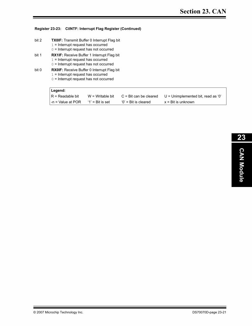
Register 23-23: CiINTF: Interrupt Flag Register (Continued)
bit 2 TX0IF: Transmit Buffer 0 Interrupt Flag bit1 = Interrupt request has occurred0 = Interrupt request has not occurred
bit 1 RX1IF: Receive Buffer 1 Interrupt Flag bit1 = Interrupt request has occurred0 = Interrupt request has not occurred
bit 0 RX0IF: Receive Buffer 0 Interrupt Flag bit1 = Interrupt request has occurred0 = Interrupt request has not occurred
Legend:R = Readable bit W = Writable bit C = Bit can be cleared U = Unimplemented bit, read as ‘0’-n = Value at POR ‘1’ = Bit is set ‘0’ = Bit is cleared x = Bit is unknown
© 2007 Microchip Technology Inc. DS70070D-page 23-21

dsPIC30F Fam
ily Reference M
anual
DS
70070D-page 23-22
© 2003 M
icrochip Technology Inc.
4 Bit 3 Bit 2 Bit 1 Bit 0 Reset
— EXIDE xxxx
<13:6> xxxx
— — — — xxxx
— — — — xxxx
— EXIDE xxxx
<13:6> xxxx
— — — — xxxx
— — — — xxxx
— EXIDE xxxx
<13:6> xxxx
— — — — xxxx
— — — — xxxx
— EXIDE xxxx
<13:6> xxxx
— — — — xxxx
— — — — xxxx
— EXIDE xxxx
<13:6> xxxx
— — — — xxxx
— — — — xxxx
— EXIDE xxxx
<13:6> xxxx
— — — — xxxx
— — — — xxxx
— MIDE xxxx
<13:6> xxxx
— — — — xxxx
— — — — xxxx
— MIDE xxxx
<13:6> xxxx
— — — — xxxx
— — — — xxxx
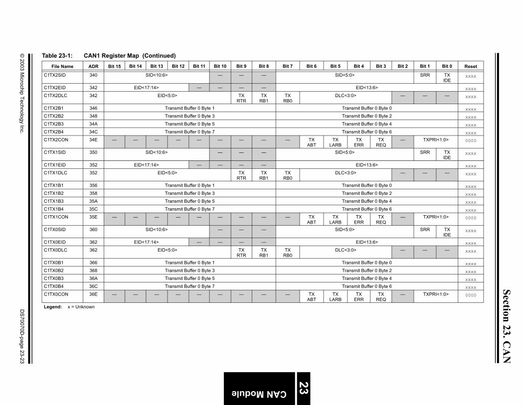
23.3 Register Maps
Table 23-1: CAN1 Register Map
File Name ADR Bit 15 Bit 14 Bit 13 Bit 12 Bit 11 Bit 10 Bit 9 Bit 8 Bit 7 Bit 6 Bit 5 Bit
C1RXF0SID 300 — — — SID<10:6> SID<5:0>
C1RXF0EIDH 302 — — — — EID<17:14> EID
C1RXF0EIDL 304 EID<5:0> — — — — — —
unused 306 — — — — — — — — — — — —
C1RXF1SID 308 — — — SID<10:6> SID<5:0>
C1RXF1EIDH 30A — — — — EID<17:14> EID
C1RXF1EIDL 30C EID<5:0> — — — — — —
Unused 30E — — — — — — — — — — — —
C1RXF2SID 310 — — — SID<10:6> SID<5:0>
C1RXF2EIDH 312 — — — — EID<17:14> EID
C1RXF2EIDL 314 EID<5:0> — — — — — —
Unused 316 — — — — — — — — — — — —
C1RXF3SID 318 — — — SID<10:6> SID<5:0>
C1RXF3EIDH 31A — — — — EID<17:14> EID
C1RXF3EIDL 31C EID<5:0> — — — — — —
Unused 31E — — — — — — — — — — — —
C1RXF4SID 320 — — — SID<10:6> SID<5:0>
C1RXF4EIDH 322 — — — — EID<17:14> EID
C1RXF4EIDL 324 EID<5:0> — — — — — —
Unused 326 — — — — — — — — — — — —
C1RXF5SID 328 — — — SID<10:6> SID<5:0>
C1RXF5EIDH 32A — — — — EID<17:14> EID
C1RXF5EIDL 32C EID<5:0> — — — — — —
Unused 32E — — — — — — — — — — — —
C1RXM0SID 330 — — — SID<10:6> SID<5:0>
C1RXM0EIDH 332 — — — — EID<17:14> EID
C1RXM0EIDL 334 EID<5:0> — — — — — —
Unused 336 — — — — — — — — — — — —
C1RXM1SID 338 — — — SID<10:6> SID<5:0>
C1RXM1EIDH 33A — — — — EID<17:14> EID
C1RXM1EIDL 33C EID<5:0> — — — — — —
Unused 33E — — — — — — — — — — — —
Legend: x = Unknown
© 2003 M
icrochip Technology Inc.D
S70070D
-page 23-23
Section 23. CA
N
C1 SRR TXIDE
xxxx
C1 :6> xxxx
C1 — — — xxxx
C1 r 0 Byte 0 xxxx
C1 r 0 Byte 2 xxxx
C1 r 0 Byte 4 xxxx
C1 r 0 Byte 6 xxxx
C1 TXREQ
— TXPRI<1:0> 0000
C1 SRR TXIDE
xxxx
C1 :6> xxxx
C1 — — — xxxx
C1 r 0 Byte 0 xxxx
C1 r 0 Byte 2 xxxx
C1 r 0 Byte 4 xxxx
C1 r 0 Byte 6 xxxx
C1 TXREQ
— TXPRI<1:0> 0000
C1 SRR TXIDE
xxxx
C1 :6> xxxx
C1 — — — xxxx
C1 r 0 Byte 0 xxxx
C1 r 0 Byte 2 xxxx
C1 r 0 Byte 4 xxxx
C1 r 0 Byte 6 xxxx
C1 TXREQ
— TXPRI<1:0> 0000
TaBit 3 Bit 2 Bit 1 Bit 0 Reset
Le
CAN Module
23
TX2SID 340 SID<10:6> — — — SID<5:0>
TX2EID 342 EID<17:14> — — — — EID<13
TX2DLC 342 EID<5:0> TXRTR
TXRB1
TXRB0
DLC<3:0>
TX2B1 346 Transmit Buffer 0 Byte 1 Transmit Buffe
TX2B2 348 Transmit Buffer 0 Byte 3 Transmit Buffe
TX2B3 34A Transmit Buffer 0 Byte 5 Transmit Buffe
TX2B4 34C Transmit Buffer 0 Byte 7 Transmit Buffe
TX2CON 34E — — — — — — — — — TXABT
TXLARB
TXERR
TX1SID 350 SID<10:6> — — — SID<5:0>
TX1EID 352 EID<17:14> — — — — EID<13
TX1DLC 352 EID<5:0> TXRTR
TXRB1
TXRB0
DLC<3:0>
TX1B1 356 Transmit Buffer 0 Byte 1 Transmit Buffe
TX1B2 358 Transmit Buffer 0 Byte 3 Transmit Buffe
TX1B3 35A Transmit Buffer 0 Byte 5 Transmit Buffe
TX1B4 35C Transmit Buffer 0 Byte 7 Transmit Buffe
TX1CON 35E — — — — — — — — — TXABT
TXLARB
TXERR
TX0SID 360 SID<10:6> — — — SID<5:0>
TX0EID 362 EID<17:14> — — — — EID<13
TX0DLC 362 EID<5:0> TXRTR
TXRB1
TXRB0
DLC<3:0>
TX0B1 366 Transmit Buffer 0 Byte 1 Transmit Buffe
TX0B2 368 Transmit Buffer 0 Byte 3 Transmit Buffe
TX0B3 36A Transmit Buffer 0 Byte 5 Transmit Buffe
TX0B4 36C Transmit Buffer 0 Byte 7 Transmit Buffe
TX0CON 36E — — — — — — — — — TXABT
TXLARB
TXERR
ble 23-1: CAN1 Register Map (Continued)
File Name ADR Bit 15 Bit 14 Bit 13 Bit 12 Bit 11 Bit 10 Bit 9 Bit 8 Bit 7 Bit 6 Bit 5 Bit 4
gend: x = Unknown

dsPIC30F Fam
ily Reference M
anual
DS
70070D-page 23-24
© 2003 M
icrochip Technology Inc.
SRR RXIDE
xxxx
<13:6> xxxx
0DLC<3:0> xxxx
Buffer 1 Byte 0 xxxx
Buffer 1 Byte 2 xxxx
Buffer 1 Byte 4 xxxx
Buffer 1 Byte 6 xxxx
RRX
RTRR0
FILHIT<2:0> 0000
SRR RXIDE
xxxx
<13:6> xxxx
0DLC<3:0> xxxx
Buffer 0 Byte 0 xxxx
Buffer 0 Byte 2 xxxx
Buffer 0 Byte 4 xxxx
Buffer 0 Byte 6 xxxx
RRX
RTRR0
RXB0DBEN
JTOFF FILHIT0
0000
ICODE<2:0> — 0480
BRP<5:0> 0000
<2:0> PRSEG<2:0> 0000
2 TXB1IF
TXB0IF
RXB1IF
RXB0IF
0000
2 TXB1IE
TXB0IE
RXB1IE
RXB0IE
0000
Error Counter 0000
— — — — xxxx
4 Bit 3 Bit 2 Bit 1 Bit 0 Reset
C1RX1SID 370 — — — SID<10:6> SID<5:0>
C1RX1EID 372 — — — — EID<17:14> EID
C1RX1DLC 374 EID<0:5> RXRTR
RXRB1
— — — RXRB
C1RX1B1 376 Receive Buffer 1 Byte 1 Receive
C1RX1B2 378 Receive Buffer 1 Byte 3 Receive
C1RX1B3 37A Receive Buffer 1 Byte 5 Receive
C1RX1B4 37C Receive Buffer 1 Byte 7 Receive
C1RX1CON 37E — — — — — — — — RXFUL
— — RXER
C1RX1SID 380 — — — SID<10:6> SID<5:0>
C1RX1EID 382 — — — — EID<17:14> EID
C1RX1DLC 384 EID<0:5> RXRTR
RXRB1
— — — RXRB
C1RX0B1 386 Receive Buffer 0 Byte 1 Receive
C1RX0B2 388 Receive Buffer 0 Byte 3 Receive
C1RX0B3 38A Receive Buffer 0 Byte 5 Receive
C1RX0B4 38C Receive Buffer 0 Byte 7 Receive
C1RX0CON 38E — — — — — — — — RXFUL
— — RXER
C1CTRL 390 CANCAP
— CSIDL
ABAT CANCKS
REQOP<2:0> OPMODE<2:0> —
C1CFG1 392 — — — — — — — — SJW<1:0>S
C1CFG2 394 — WAKFIL
— — — SEG2PH<2:0> SEG2PHTS
SAM SEG1PH
C1INTF 396 RXB0OVR
RXB1OVR
TXBO TXBP RXBP TXWARN
RXWARN
EWARN
IVRIF
WAKIF
ERRIF
TXBIF
C1INTE 398 — — — — — — — — IVRIE
WAKIE
ERRIE
TXBIE
C1EC 39A Transmit Error Counter Receive
Reserved 39C3FE
— — — — — — — — — — — —
Table 23-1: CAN1 Register Map (Continued)
File Name ADR Bit 15 Bit 14 Bit 13 Bit 12 Bit 11 Bit 10 Bit 9 Bit 8 Bit 7 Bit 6 Bit 5 Bit
Legend: x = Unknown

© 2003 M
icrochip Technology Inc.D
S70070D
-page 23-25
Section 23. CA
N
TaBit 3 Bit 2 Bit 1 Bit 0 Reset
C2 — EXIDE xxxx
C2 :6> xxxx
C2 — — — — xxxx
Un — — — — xxxx
C2 — EXIDE xxxx
C2 :6> xxxx
C2 — — — — xxxx
Un — — — — xxxx
C2 — EXIDE xxxx
C2 :6> xxxx
C2 — — — — xxxx
Un — — — — xxxx
C2 — EXIDE xxxx
C2 :6> xxxx
C2 — — — — xxxx
Un — — — — xxxx
C2 — EXIDE xxxx
C2 :6> xxxx
C2 — — — — xxxx
Un — — — — xxxx
C2 — EXIDE xxxx
C2 :6> xxxx
C2 — — — — xxxx
Un — — — — xxxx
C2 — MIDE xxxx
C2 :6> xxxx
C2 — — — — xxxx
Un — — — — xxxx
C2 — MIDE xxxx
C2 :6> xxxx
C2 — — — — xxxx
Un — — — — xxxx
Le
CAN Module
23
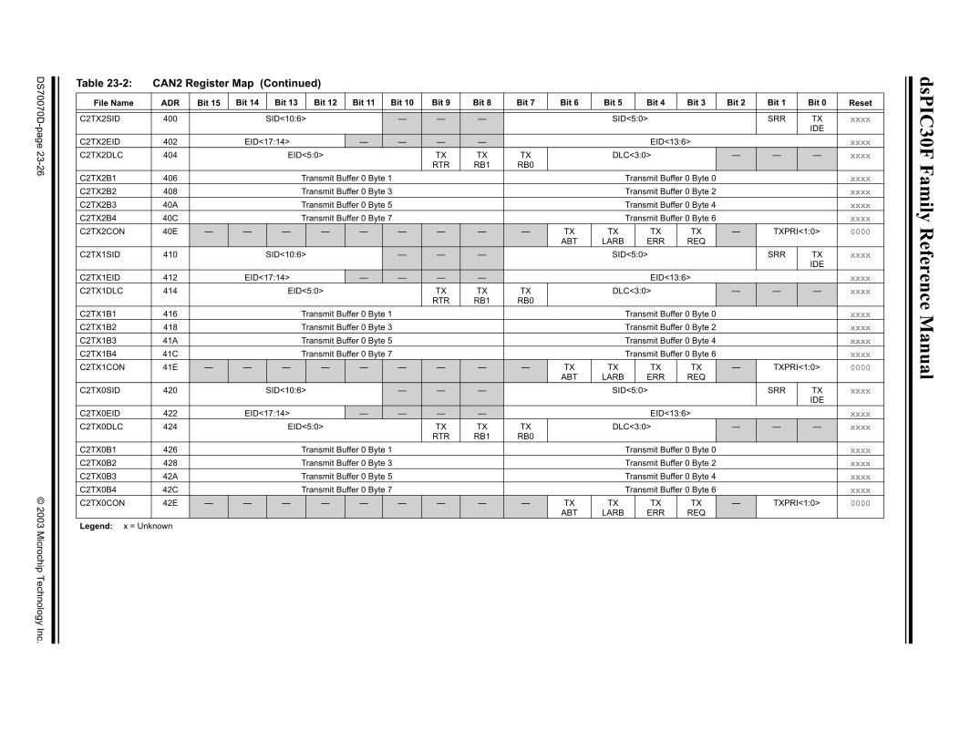
ble 23-2: CAN2 Register Map
File Name ADR Bit 15 Bit 14 Bit 13 Bit 12 Bit 11 Bit 10 Bit 9 Bit 8 Bit 7 Bit 6 Bit 5 Bit 4
RXF0SID 3C0 — — — SID<10:6> SID<5:0>RXF0EIDH 3C2 — — — — EID<17:14> EID<13RXF0EIDL 3C4 EID<5:0> — — — — — —used 3C6 — — — — — — — — — — — —RXF1SID 3C8 — — — SID<10:6> SID<5:0>RXF1EIDH 3CA — — — — EID<17:14> EID<13RXF1EIDL 3CC EID<5:0> — — — — — —used 3CE — — — — — — — — — — — —RXF2SID 3D0 — — — SID<10:6> SID<5:0>RXF2EIDH 3D2 — — — — EID<17:14> EID<13RXF2EIDL 3D4 EID<5:0> — — — — — —used 3D6 — — — — — — — — — — — —RXF3SIDH 3D8 — — — SID<10:6> SID<5:0>RXF3EID 3DA — — — — EID<17:14> EID<13RXF3EIDL 3DC EID<5:0> — — — — — —used 3DE — — — — — — — — — — — —RXF4SID 3E0 — — — SID<10:6> SID<5:0>RXF4EIDH 3E2 — — — — EID<17:14> EID<13RXF4EIDL 3E4 EID<5:0> — — — — — —used 3E6 — — — — — — — — — — — —RXF5SID 3E8 — — — SID<10:6> SID<5:0>RXF5EIDH 3EA — — — — EID<17:14> EID<13RXF5EIDL 3EC EID<5:0> — — — — — —used 3EE — — — — — — — — — — — —RXM0SID 3F0 — — — SID<10:6> SID<5:0>RXM0EIDH 3F2 — — — — EID<17:14> EID<13RXM0EIDL 3F4 EID<5:0> — — — — — —used 3F6 — — — — — — — — — — — —RXM1SID 3F8 — — — SID<10:6> SID<5:0>RXM1EIDH 3FA — — — — EID<17:14> EID<13RXM1EIDL 3FC EID<5:0> — — — — — —used 3FE — — — — — — — — — — — —gend: x = Unknown
dsPIC30F Fam
ily Reference M
anual
DS
70070D-page 23-26
© 2003 M
icrochip Technology Inc.
SRR TXIDE
xxxx
<13:6> xxxx
— — — xxxx
Buffer 0 Byte 0 xxxx
Buffer 0 Byte 2 xxxx
Buffer 0 Byte 4 xxxx
Buffer 0 Byte 6 xxxx
RTX
REQ— TXPRI<1:0> 0000
SRR TXIDE
xxxx
<13:6> xxxx
— — — xxxx
Buffer 0 Byte 0 xxxx
Buffer 0 Byte 2 xxxx
Buffer 0 Byte 4 xxxx
Buffer 0 Byte 6 xxxx
RTX
REQ— TXPRI<1:0> 0000
SRR TXIDE
xxxx
<13:6> xxxx
— — — xxxx
Buffer 0 Byte 0 xxxx
Buffer 0 Byte 2 xxxx
Buffer 0 Byte 4 xxxx
Buffer 0 Byte 6 xxxx
RTX
REQ— TXPRI<1:0> 0000
4 Bit 3 Bit 2 Bit 1 Bit 0 Reset
C2TX2SID 400 SID<10:6> — — — SID<5:0>
C2TX2EID 402 EID<17:14> — — — — EIDC2TX2DLC 404 EID<5:0> TX
RTRTX
RB1TX
RB0DLC<3:0>
C2TX2B1 406 Transmit Buffer 0 Byte 1 Transmit C2TX2B2 408 Transmit Buffer 0 Byte 3 Transmit C2TX2B3 40A Transmit Buffer 0 Byte 5 Transmit C2TX2B4 40C Transmit Buffer 0 Byte 7 Transmit C2TX2CON 40E — — — — — — — — — TX
ABTTX
LARBTX
ERC2TX1SID 410 SID<10:6> — — — SID<5:0>
C2TX1EID 412 EID<17:14> — — — — EIDC2TX1DLC 414 EID<5:0> TX
RTRTX
RB1TX
RB0DLC<3:0>
C2TX1B1 416 Transmit Buffer 0 Byte 1 Transmit C2TX1B2 418 Transmit Buffer 0 Byte 3 Transmit C2TX1B3 41A Transmit Buffer 0 Byte 5 Transmit C2TX1B4 41C Transmit Buffer 0 Byte 7 Transmit C2TX1CON 41E — — — — — — — — — TX
ABTTX
LARBTX
ERC2TX0SID 420 SID<10:6> — — — SID<5:0>
C2TX0EID 422 EID<17:14> — — — — EIDC2TX0DLC 424 EID<5:0> TX
RTRTX
RB1TX
RB0DLC<3:0>
C2TX0B1 426 Transmit Buffer 0 Byte 1 Transmit C2TX0B2 428 Transmit Buffer 0 Byte 3 Transmit C2TX0B3 42A Transmit Buffer 0 Byte 5 Transmit C2TX0B4 42C Transmit Buffer 0 Byte 7 Transmit C2TX0CON 42E — — — — — — — — — TX
ABTTX
LARBTX
ER
Table 23-2: CAN2 Register Map (Continued)
File Name ADR Bit 15 Bit 14 Bit 13 Bit 12 Bit 11 Bit 10 Bit 9 Bit 8 Bit 7 Bit 6 Bit 5 Bit
Legend: x = Unknown

© 2003 M
icrochip Technology Inc.D
S70070D
-page 23-27
Section 23. CA
N
C2 SRR RXIDE
xxxx
C2 :6> xxxx
C2 DLC<3:0> xxxx
C2 r 1 Byte 0 xxxx
C2 r 1 Byte 2 xxxx
C2 r 1 Byte 4 xxxx
C2 r 1 Byte 6 xxxx
C2 RXRTRR0
FILHIT<2:0> 0000
C2 SRR RXIDE
xxxx
C2 :6> xxxx
C2 DLC<3:0> xxxx
C2 r 0 Byte 0 xxxx
C2 r 0 Byte 2 xxxx
C2 r 0 Byte 4 xxxx
C2 r 0 Byte 6 xxxx
C2 RXRTRR0
RXB0DBEN
JTOFF FILHIT0
0000
C2 ICODE<2:0> — 0480
C2 BRP<5:0> 0000
C2 > PRSEG<2:0> 0000
C2 TXB1IF
TXB0IF
RXB1IF
RXB0IF
0000
C2 TXB1IE
TXB0IE
RXB1IE
RXB0IE
0000
C2 r Counter 0000
Re — — — — xxxx
TaBit 3 Bit 2 Bit 1 Bit 0 Reset
Le
CAN Module
23
RX1SID 430 — — — SID<10:6> SID<5:0>
RX1EID 432 — — — — EID<17:14> EID<13RX1DLC 434 EID<0:5> RX
RTRRX
RB1— — — RX
RB0RX1B1 436 Receive Buffer 1 Byte 1 Receive BuffeRX1B2 438 Receive Buffer 1 Byte 3 Receive BuffeRX1B3 43A Receive Buffer 1 Byte 5 Receive BuffeRX1B4 43C Receive Buffer 1 Byte 7 Receive BuffeRX1CON 43E — — — — — — — — RX
FUL— — RX
ERR
RX1SID 440 — — — SID<10:6> SID<5:0>
RX1EID 442 — — — — EID<17:14> EID<13RX1DLC 444 EID<0:5> RX
RTRRX
RB1— — — RX
RB0RX0B1 446 Receive Buffer 0 Byte 1 Receive BuffeRX0B2 448 Receive Buffer 0 Byte 3 Receive BuffeRX0B3 44A Receive Buffer 0 Byte 5 Receive BuffeRX0B4 44C Receive Buffer 0 Byte 7 Receive BuffeRX0CON 44E — — — — — — — — RX
FUL— — RX
ERR
CTRL 450 CANCAP
— CSIDL
ABAT CANCKS
REQOP<2:0> OPMODE<2:0> —
CFG1 452 — — — — — — — — SJW<1:0>SCFG2 454 — WAK
FIL— — — SEG2PH<2:0> SEG2
PHTSSAM SEG1PH<2:0
INTF 456 RXB0OVR
RXB1OVR
TXBO TXBP RXBP TXWARN
RXWARN
EWARN
IVRIF
WAKIF
ERRIF
TXB2IF
INTE 458 — — — — — — — — IVRIE
WAKIE
ERRIE
TXB2IE
EC 45A Transmit Error Counter Receive Erroserved 45C
4FE— — — — — — — — — — — —
ble 23-2: CAN2 Register Map (Continued)
File Name ADR Bit 15 Bit 14 Bit 13 Bit 12 Bit 11 Bit 10 Bit 9 Bit 8 Bit 7 Bit 6 Bit 5 Bit 4
gend: x = Unknown

dsPIC30F Family Reference Manual
23.4 CAN Module FeaturesThe CAN module is a communication controller implementing the CAN 2.0A/B protocol asdefined in the BOSCH specification. The module will support CAN 1.2, CAN 2.0A, CAN 2.0BPassive and CAN 2.0B Active versions of the protocol. The module implementation is a Full CANsystem.
The module features are as follows:
• Implementation of the CAN protocol CAN 1.2, CAN 2.0A and CAN 2.0B • Standard and extended data frames• Data length from 0-8 bytes• Programmable bit rate up to 1 Mbit/sec• Support for remote data frames• Double buffered receiver with two prioritized received message storage buffers• Six full (standard/extended identifier) acceptance filters, 2 associated with the high priority
receive buffer and 4 associated with the low priority receive buffer• Two full acceptance filter masks, one each associated with the high and low priority receive
buffers• Three Transmit Buffers with application specified prioritization and abort capability• Programmable wake-up functionality with integrated low-pass filter• Programmable Loopback mode supports self-test operation• Signaling via interrupt capabilities for all CAN receiver and transmitter error states• Programmable clock source• Programmable link to input capture module for time-stamping and network synchronization• Low-Power Sleep mode
DS70070D-page 23-28 © 2007 Microchip Technology Inc.

Section 23. CANC
AN
Module
23
23.5 CAN Module ImplementationThe CAN bus module consists of a Protocol Engine and message buffering and control. TheProtocol Engine can best be understood by defining the types of data frames to be transmittedand received by the module. These blocks are shown in Figure 23-2.
Figure 23-2: CAN Buffers and Protocol Engine Block Diagram
Acceptance FilterRXF2
RXB1
Accept
Accept
Identifier
Data Field Data Field
Identifier
Acceptance MaskRXM1
Acceptance FilterRXF3
Acceptance FilterRXF4
Acceptance FilterRXF5
Acceptance MaskRXM0
Acceptance FilterRXF0
Acceptance FilterRXF1
RXB0
TXR
EQ
TXB2
TXA
BT
TXLA
RB
TXE
RR
TXP
RI
ME
SSA
GE
MessageQueueControl
Transmit Byte Sequencer
TXR
EQ
TXB1
TXA
BT
TXLA
RB
TXE
RR
TXP
RI
ME
SSA
GE
TXR
EQ
TXB0
TXA
BT
TXLA
RB
TXE
RR
TXP
RI
ME
SSA
GE
Receive ShiftTransmit Shift
ReceiveError
TransmitError
Protocol
RERRCNT
TERRCNT
ErrPasBusOff
FiniteState
Machine
Counter
Counter
TransmitLogic
BitTimingLogic
CxTX CxRX
Bit TimingGenerator
PROTOCOLENGINE
BUFFERS
CRC CheckCRC Generator
Note: x = 1 or 2
MessageAssembly
Buffer
© 2007 Microchip Technology Inc. DS70070D-page 23-29

dsPIC30F Family Reference Manual
23.5.1 CAN Message Formats
The CAN protocol engine handles all functions for receiving and transmitting messages on theCAN bus. Messages are transmitted by first loading the appropriate data registers. Status anderrors can be checked by reading the appropriate registers. Any message detected on the CANbus is checked for errors and then matched against filters to see if it should be received andstored in one of the two receive registers.
The CAN Module supports the following frame types:
• Standard Data Frame• Extended Data Frame• Remote Frame• Error Frame• Interframe Space
23.5.1.1 Standard Data Frame
A standard data frame is generated by a node when the node wishes to transmit data. Thestandard CAN data frame is shown in Figure 23-3. In common with all other frames, the framebegins with a Start-Of-Frame bit (SOF-dominant state) for hard synchronization of all nodes.
The SOF is followed by the Arbitration field consisting of 12 bits, the 11-bit identifier (reflectingthe contents and priority of the message) and the Remote Transmission Request bit (RTR bit).The RTR bit is used to distinguish a data frame (RTR-dominant) from a remote frame.
The next field is the Control field, consisting of 6 bits. The first bit of this field is called the IdentifierExtension (IDE) bit and is at dominant state to specify that the frame is a standard frame. Thefollowing bit is reserved by the CAN protocol, RB0, and defined as a dominant bit. Theremaining 4 bits of the Control field are the Data Length Code (DLC) and specify the number ofbytes of data contained in the message.
The data being sent follows in the Data field which is of the length defined by the DLC above(0-8 bytes).
The Cyclic Redundancy Check (CRC) field follows and is used to detect possible transmissionerrors. The CRC field consists of a 15-bit CRC sequence and a delimiter bit. The message iscompleted by the End-Of-Frame (EOF) field, which consists of seven recessive bits with nobit-stuffing.
The final field is the Acknowledge field. During the ACK Slot bit the transmitting node sends outa recessive bit. Any node that has received an error free frame acknowledges the correctreception of the frame by sending back a dominant bit (regardless of whether the node isconfigured to accept that specific message or not). The recessive Acknowledge Delimitercompletes the Acknowledge Slot and may not be overwritten by a dominant bit, except when anerror frame occurs.
23.5.1.2 Extended Data Frame
In the extended CAN data frame, as shown in Figure 23-4, the Start-Of-Frame bit (SOF) isfollowed by the Arbitration Field consisting of 38 bits. The first 11 bits are the 11 Most Significantbits of the 29-bit identifier (“Base-lD”). These 11 bits are followed by the Substitute RemoteRequest bit (SRR), which is transmitted as recessive. The SRR is followed by the lDE bit whichis recessive to denote that the frame is an extended CAN frame. It should be noted from this, thatif arbitration remains unresolved after transmission of the first 11 bits of the identifier, and one ofthe nodes involved in arbitration is sending a standard CAN frame (11-bit identifier), then thestandard CAN frame will win arbitration due to the assertion of a dominant lDE bit. Also, the SRRbit in an extended CAN frame must be recessive to allow the assertion of a dominant RTR bit bya node that is sending a standard CAN remote frame. The SRR and lDE bits are followed by theremaining 18 bits of the identifier (“lD-Extension”) and a dominant RTR bit.
DS70070D-page 23-30 © 2007 Microchip Technology Inc.

Section 23. CANC
AN
Module
23
To enable standard and extended frames to be sent across a shared network, it is necessary tosplit the 29-bit extended message identifier into 11-bit (Most Significant) and 18-bit (LeastSignificant) sections. This split ensures that the Identifier Extension bit (lDE) can remain at thesame bit position in both standard and extended frames.
The next field is the Control field, consisting of 6 bits. The first 2 bits of this field are reserved andare at dominant state. The remaining 4 bits of the Control field are the Data Length Code (DLC)and specify the number of data bytes.
The remaining portion of the frame (Data field, CRC field, Acknowledge field, End-Of-Frame andintermission) is constructed in the same way as for a standard data frame.
23.5.1.3 Remote Frame
A data transmission is usually performed on an autonomous basis with the data source node (Forexample, a sensor sending out a data frame). It is possible however for a destination node torequest the data from the source. For this purpose, the destination node sends a “remote frame”with an identifier that matches the identifier of the required data frame. The appropriate datasource node will then send a data frame as a response to this remote request.
There are two differences between a remote frame and a data frame, shown in Figure 23-5. First,the RTR bit is at the recessive state and second there is no Data field. In the very unlikely eventof a data frame and a remote frame with the same identifier being transmitted at the same time,the data frame wins arbitration due to the dominant RTR bit following the identifier. In this way,the node that transmitted the remote frame receives the desired data immediately.
23.5.1.4 The Error Frame
An error frame is generated by any node that detects a bus error. An error frame, shown inFigure 23-6, consists of 2 fields, an error flag field followed by an Error Delimiter field. The ErrorDelimiter consists of 8 recessive bits and allows the bus nodes to restart bus communicationscleanly after an error. There are two forms of error flag fields. The form of the error flag fielddepends on the error status of the node that detects the error.
If an error-active node detects a bus error then the node interrupts transmission of the currentmessage by generating an active error flag. The active error flag is composed of six consecutivedominant bits. This bit sequence actively violates the bit-stuffing rule. All other stations recognizethe resulting bit-stuffing error and in turn generate error frames themselves, called Error EchoFlags. The error flag field therefore consists of between six and twelve consecutive dominant bits(generated by one or more nodes). The Error Delimiter field completes the error frame. Aftercompletion of the error frame, bus activity retains to normal and the interrupted node attempts toresend the aborted message.
If an error passive node detects a bus error then the node transmits an Error Passive flagfollowed, again, by the Error Delimiter field. The Error Passive flag consists of six consecutiverecessive bits. From this it follows that, unless the bus error is detected by the transmitting nodeor other error active receiver that is actually transmitting, the transmission of an error frame byan error passive node will not affect any other node on the network. If the bus master nodegenerates an error passive flag then this may cause other nodes to generate error frames dueto the resulting bit-stuffing violation. After transmission of an error frame, an error passive nodemust wait for 6 consecutive recessive bits on the bus before attempting to rejoin buscommunications.
23.5.1.5 The Interframe Space
Interframe Space separates a proceeding frame (of whatever type) from a following data orremote frame. lnterframe Space is composed of at least 3 recessive bits, called the intermission.This is provided to allow nodes time for internal processing of the message by receiving nodesbefore the start of the next message frame. After the intermission, the bus line remains in therecessive state (bus idle) until the next transmission starts.
If the transmitting node is in the error passive state, an additional 8 recessive bit times will beinserted in the Interframe Space before any other message is transmitted by that node. This timeperiod is called the Suspend Transmit field. The Suspend Transmit field allows additional delaytime for other transmitting nodes to take control of the bus.
© 2007 Microchip Technology Inc. DS70070D-page 23-31

dsPIC30F Family Reference Manual
Figure 23-3: Standard Data Frame
11
11
11
11
11
11
11
11
11
11
11
11
0
INT
Susp
end
Tran
smit
bus
Idle
Any
Fra
me
Inte
r-Fra
me
Spac
e
Start-Of-Frame
Dat
a Fr
ame
orR
emot
e Fr
ame
38
00
00
00
00
00
00
11
11
11
11
1
Start-Of-Frame
Dat
a Fr
ame
(num
ber o
f bits
=44
+8
N)
12Ar
bitra
tion
Fiel
d
ID 10
11ID3
ID0
Iden
tifie
r
Mes
sage
Filte
ring
Stor
ed in
Buf
fers
RTRIDERB0DLC3
DLC0
6
4
Con
trol
Fiel
d
Dat
aLe
ngth
Cod
e
Reserved Bits
8N
(≤N≤
8)D
ata
Fiel
d
88
Stor
ed in
Tra
nsm
it/R
ecei
ve B
uffe
rs
Bit-S
tuffi
ng
16C
RC
Fie
ld
15 CR
C
7
End
-Of-
Fram
e
CRC DelAcknowledgmentACK Del 1
11
11
11
11
11
11
11
11
11
11
11
10
INT
Sus
pend
Tran
smit
bus
Idle
Any
Fram
e
Inte
r-Fr
ame
Spac
e
Start-Of-Frame
Dat
a Fr
ame
orR
emot
e Fr
ame
38
DS70070D-page 23-32 © 2007 Microchip Technology Inc.

Section 23. CANC
AN
Module
23
Figure 23-4: Extended Data Format
11
11
10
bus
Idle
Start-Of-Frame
Dat
a Fr
ame
orR
emot
e Fr
ame
01
10
00
00
00
00
00
00
00
00
00
00
00
00
1
Start-Of-Frame
Arbi
tratio
n Fi
eld
32
11
ID10
ID3
ID0IDE
Iden
tifie
r
Mes
sage
Filte
ring
Stor
ed in
Buf
fers
SRREID17
EID0RTRRB1RB0DLC3
18
DLC0
6C
ontro
lFi
eld 4
Reserved bits
Dat
aLe
ngth
Cod
e Stor
ed in
Tra
nsm
it/R
ecei
ve B
uffe
rs
88
Ext
ende
d D
ata
Fram
e (n
umbe
r of b
its=
64+
8N
)8
N (N
≤ 8)
Dat
a Fi
eld
11
11
11
11
16C
RC
Fie
ld
15 CR
C
CRC DelAcknowledgmentACK Del
End
-Of-
Fram
e
7
Bit-
Stuf
fing
11
11
11
11
11
11
11
11
11
11
11
11
0
INT
Susp
end
Tran
smit
bus
Idle
Any
Fram
e
Inte
r-Fra
me
Spac
e
Start-Of-Frame
Dat
a Fr
ame
orR
emot
e Fr
ame
38
Ext
ende
d Id
entif
ier
1
© 2007 Microchip Technology Inc. DS70070D-page 23-33

dsPIC30F Family Reference Manual
Figure 23-5: Remote Data Frame
Iden
tifie
r
Mes
sage
Filte
ring
Stor
ed in
Buf
fers
Dat
aLe
ngth
Cod
eReserved Bits B
it-St
uffin
g
11
11
11
11
11
11
11
11
11
11
11
11
0
INT
Sus
pend
Tran
smit
bus
Idle
Any
Fram
e
Inte
r-Fr
ame
Spac
e
Start-Of-Frame
Dat
a Fr
ame
orR
emot
e Fr
ame
38
01
00
11
11
11
11
1
Start-Of-Frame
Rem
ote
Fram
e (n
umbe
r of b
its=
44)
12Ar
bitra
tion
Fiel
d
ID 1011
ID0RTRIDERB0DLC3
DLC0
6
4
Con
trol
Fiel
d
16C
RC
Fie
ld
15 CR
C
7
End
-Of-
Fram
e
CRC DelAcknowledgmentACK Del 1
11
11
11
11
11
11
11
11
11
11
11
10
INT
Sus
pend
Tran
smit
bus
Idle
Any
Fra
me
Inte
r-Fr
ame
Spac
e
Start-Of-Frame Dat
a Fr
ame
orR
emot
e Fr
ame
38
DS70070D-page 23-34 © 2007 Microchip Technology Inc.

Section 23. CANC
AN
Module
23
Figure 23-6: Error Frame
11
11
11
11
11
11
11
11
11
11
11
11
0
INT
Susp
end
Tran
smit
bus
Idle
Any
Fra
me
Inte
r-Fra
me
Spac
e
Start-Of-Frame
Dat
a Fr
ame
orR
emot
e Fr
ame
38
00
00
Start-Of-Frame
Inte
rrupt
ed D
ata
Fram
e
12Ar
bitra
tion
Fiel
d
ID 1011
ID3
ID0
Iden
tifie
r
Mes
sage
Filte
ring
RTRIDERB0DLC3
DLC0
6
4
Con
trol
Fiel
d
Dat
aLe
ngth
Cod
e
Reserved Bits
8N (≤
N ≤
8)
Dat
a Fi
eld
88
Bit-
Stuf
fing
11
11
11
11
11
11
11
11
11
11
11
11
0
INT
Sus
pend
Tran
smit
bus
Idle
Any
Fram
e
Inte
r-Fra
me
Spac
e
Star-Of-Frame
Dat
a Fr
ame
orR
emot
e Fr
ame
38
00
00
00
00
01
11
11
11
10
Dat
a Fr
ame
orR
emot
e Fr
ame
Err
or F
ram
e
6E
rror
Flag
≤ 6
Echo
Erro
rFl
ag
8E
rror
Del
imite
rIn
ter-
Fram
e Sp
ace
© 2007 Microchip Technology Inc. DS70070D-page 23-35

dsPIC30F Family Reference Manual
23.6 CAN Module Operation ModesThe CAN Module can operate in one of several Operation modes selected by the user. Thesemodes include:
• Normal Operation mode• Disable mode• Loopback mode• Listen Only mode• Configuration mode• Listen to All Messages mode
Modes are requested by setting the REQOP<2:0> bits (CiCTRL<10:8>). Entry into a mode isacknowledged by monitoring the OPMODE<2:0> bits (CiCTRL<7:5>). The module does notchange the mode and the OPMODE bits until a change in mode is acceptable, generally duringbus idle time which is defined as at least 11 consecutive recessive bits.
23.6.1 Normal Operation Mode
Normal Operation mode is selected when REQOP<2:0> = ‘000’. In this mode, the module isactivated, the I/O pins will assume the CAN bus functions. The module will transmit and receiveCAN bus messages as described in subsequent sections.
23.6.2 Disable Mode
The CAN module will not transmit or receive in Disable mode. The module has the ability to setthe WAKIF bit due to bus activity, however any pending interrupts will remain and the errorcounters will retain their value.
If the REQOP<2:0> bits (CiCTRL<10:8>) = ‘001’, the module will enter the Module Disablemode. This mode is similar to disabling other peripheral modules by turning off the moduleenables. This causes the module internal clock to stop unless the module is active (i.e., receivingor transmitting a message). If the module is active, the module will wait for 11 recessive bitson the CAN bus, detect that condition as an idle bus, then accept the module disable command.When the OPMODE<2:0> bits (CiCTRL<7:5>) = ‘001’, this indicates that the modulesuccessfully entered Module Disable mode (see Figure 23-7).
The WAKIF interrupt is the only module interrupt that is still active in the Module Disable mode.If the WAKIE bit (CiINTE<6>) is set, the processor will receive an interrupt whenever the CANbus detects a dominant state, as occurs with a Start-Of-Frame (SOF).
The I/O pins will revert to normal I/O function when the module is in the Module Disable mode.
Note: Typically, if the CAN module is allowed to transmit in a particular mode of operationand a transmission is requested immediately after the CAN module has beenplaced in that mode of operation, the module waits for 11 consecutive recessive bitson the bus before starting transmission. If the user switches to Disable Mode withinthis 11-bit period, then this transmission is aborted and the corresponding TXABTbit is set and TXREQ bit is cleared.
DS70070D-page 23-36 © 2007 Microchip Technology Inc.

Section 23. CANC
AN
Module
23
Figure 23-7: Entering and Exiting Module Disable Mode
23.6.3 Loopback Mode
If the Loopback mode is activated, the module will connect the internal transmit signal to theinternal receive signal at the module boundary. The transmit and receive pins revert to theirPORT I/O function.
The transmitter will receive an acknowledge for its sent messages. Special hardware willgenerate an acknowledge for the transmitter.
23.6.4 Listen Only Mode
Listen Only mode and Loopback modes are special cases of Normal Operation mode to allowsystem debug. If the Listen Only mode is activated, the module on the CAN bus is passive. Thetransmitter buffers revert to the PORT I/O function. The receive pins remain as inputs to the CANmodule. For the receiver, no error flags or Acknowledge signals are sent. The error counters aredeactivated in this state. The Listen Only mode can be used for detecting the baud rate on theCAN bus. To use this, it is necessary that there are at least two further nodes that communicatewith each other. The baud rate can be detected empirically by testing different values. This modeis also useful as a bus monitor without influencing the data traffic.
1 2 4 5
- Processor writes REQOP<2:0> while module receiving/transmitting message. Module continues with CAN message. - Module detects 11 recessive bits. Module acknowledges Disable mode and sets OPMODE<2:0> bits. Module disables.
- Processor writes REQOP<2:0> during CAN bus activity. Module waits for 11 recessive bits before accepting activate. - Module detects 11 recessive bits. Module acknowledges Normal mode and sets OPMODE<2:0> bits. Module activates.
OSC1
CAN bus
CAN ModuleDisabled
3
001
001000
000 000
000
- CAN bus message will set WAKIF bit. If WAKIE = ’1’, processor will vector to the interrupt address. CAN message ignored.
WAKIF
WAKIE
12
34
5
OPMODE<2:0>
REQOP<2:0>
© 2007 Microchip Technology Inc. DS70070D-page 23-37
dsPIC30F Family Reference Manual
23.6.5 Configuration Mode
In the Configuration mode, the module will not transmit or receive. The error counters are clearedand the interrupt flags remain unchanged. The programmer will have access to configurationregisters that are access restricted in other modes.
After a device Reset the CAN module is in the Configuration mode (OPMODE<2:0> = ‘100’). Theerror counters are cleared and all registers contain the Reset values. It should be ensured thatthe initialization is performed before REQOP<2> bit is cleared.
The CAN module has to be initialized before its activation. This is only possible if the module isin the Configuration mode. The Configuration mode is requested by setting the REQOP<2> bit.Only when the Status bit OPMODE<2> has a high level, the initialization can be performed.Afterwards the configuration registers and the acceptance mask registers and the acceptancefilter registers can be written. The module is activated by clearing the control bits REQOP<2:0>.
The module will protect the user from accidentally violating the CAN protocol through program-ming errors. All registers which control the configuration of the module can not be modified whilethe module is on-line. The CAN module will not be allowed to enter the Configuration mode whilea transmission is taking place. The Configuration mode serves as a lock to protect the followingregisters.
• All Module Control Registers• Baud Rate and Interrupt Configuration Registers • Bus Timing Registers • Identifier Acceptance Filter Registers • Identifier Acceptance Mask Registers
23.6.6 Listen All Messages Mode
Listen All Messages mode is a special case of Normal Operation mode to allow system debug.If the Listen All Messages mode is activated, the module on the CAN bus is passive. Thetransmitter buffers revert to the PORT I/O function. The receive pins remain inputs. For thereceiver, no error flags or Acknowledge signals are sent. The error counters are deactivated inthis state. The filters are disabled. Receive Buffer 0 will receive any message transferred on thebus. This mode is useful to record all bus traffic as a bus monitor without influencing the datatraffic.
DS70070D-page 23-38 © 2007 Microchip Technology Inc.

Section 23. CANC
AN
Module
23
23.7 Message ReceptionThis subsection describes CAN module message reception.
23.7.1 Receive Buffers
The CAN bus module has three receive buffers. However, one of the receive buffers is alwayscommitted to monitoring the bus for incoming messages. This buffer is called the MessageAssembly Buffer (MAB). So there are two receive buffers visible, RXB0 and RXB1, that canessentially instantaneously receive a complete message from the protocol engine. The CPU canbe operating on one while the other is available for reception or holding a previously receivedmessage.
The MAB holds the destuffed bit stream from the bus line to allow parallel access to the wholedata or remote frame for the acceptance match test and the parallel transfer of the frame to thereceive buffers. The MAB will assemble all messages received. These messages will betransferred to the RXBn buffers only if the acceptance filter criterion are met. When a messageis received, the RXnIF flag (CiINTF<0> or CiINRF<1>) will be set. This bit can only be set by themodule when a message is received. The bit is cleared by the CPU when it has completedprocessing the message in the buffer. This bit provides a positive lockout to ensure that the CPUhas finished with the message buffer. If the RXnIE bit (CiINTE<0> or CiINTE<1>) is set, aninterrupt will be generated when a message is received.
There are 2 programmable acceptance filter masks associated with the receive buffers, one foreach buffer.
When the message is received, the FILHIT bits (CiRX0CON<0> for Receive Buffer 0 andCiRX1CON<2:0> for Receive Buffer 1) indicate the acceptance criterion for the message. Thenumber of the acceptance filter that enabled the reception will be indicated as well as a Statusbit that indicates that the received message is a remote transfer request.
Note: In the case of Receive Buffer 0, a limited number of Acceptance Filters can be usedto enable a reception. A single bit, FILHIT0 (CiRX0CON<0>) determines which ofthe 2 filters, RXF0 or RXF1, enabled the message reception.
© 2007 Microchip Technology Inc. DS70070D-page 23-39

dsPIC30F Family Reference Manual
23.7.1.1 Receive Buffer Priority
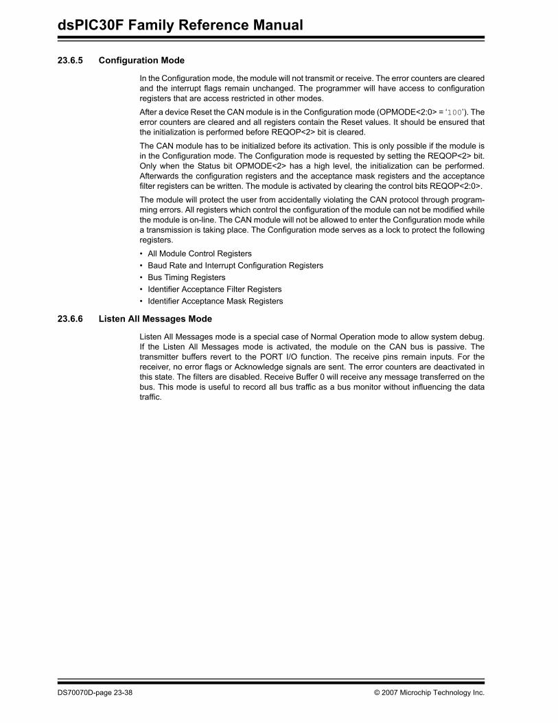
To provide flexibility, there are several acceptance filters corresponding to each receive buffer.There is also an implied priority to the receive buffers. RXB0 is the higher priority buffer and hastwo message acceptance filters associated with it. RXB1 is the lower priority buffer and has fouracceptance filters associated with it. The lower number of possible acceptance filters makes thematch on RXB0 more restrictive and implies the higher priority associated with that buffer.Additionally, if the RXB0 contains a valid message, and another valid message is received, theRXB0 can be set up such that it will not overrun and the new message for RXB0 will be placedinto RXB1. Figure 23-8 shows a block diagram of the receive buffer, while Figure 23-9 shows aflow chart of a receive operation.
Figure 23-8: The Receive Buffers
Acceptance MaskRXM1
Acceptance FilterRXF2
Acceptance FilterRXF3
Acceptance FilterRXF4
Acceptance FilterRXF5
RXB1
RXB0
Acceptance MaskRXM0
Acceptance FilterRXF0
Acceptance FilterRXF1
AcceptA
ccept
Identifier
Data Field Data Field
IdentifierMessageAssemblyBuffer
DS70070D-page 23-40 © 2007 Microchip Technology Inc.
Section 23. CANC
AN
Module
23
Figure 23-9: Receive Flowchart
START
DetectStart of
Message?
ValidMessageReceived
?
GenerateError
MessageIdentifier meetsa filter criteria
?
IsRXFUL = 0
?
Go to Start
Move message into RXB0
Set RXFUL = 1
Set FILHIT<2:0>
IsRXFUL = 0
?
Move message into RXB1
Set RXFUL = 1
Yes, meets criteriafor RXB0
Yes, meets criteriafor RXB1
No
GenerateInterrupt
Yes
Yes
No No
Yes
Yes
No
No
Yes
Yes
Frame
The RXFUL bit determines if thereceive register is empty andable to accept a new message.
No Yes
No
Generate Overrun Error:
Begin Loading Message intoMessage Assembly Buffer (MAB)
was met
IsRXnIE = 1
?
DoesRXnIE = 1
?
IsDBEN = 1
?
The DBEN bit determines ifRXB0 can roll over intoRXB1 if it is full.
Set RX0OVRGenerate Overrun Error:
Set RX1OVR
DoesERRIE = 1
?
No
Go to StartYes
NoSet FILHIT<0>according to which filter criteria
was met
Set ICODE<3:0> accordingto which receive buffer themessage was loaded into
according to which filter criteria
© 2007 Microchip Technology Inc. DS70070D-page 23-41

dsPIC30F Family Reference Manual
23.7.2 Message Acceptance Filters
The message acceptance filters and masks are used to determine if a message in the messageassembly buffer should be loaded into either of the receive buffers. Once a valid message hasbeen received into the message assembly buffer, the identifier fields of the message are com-pared to the filter values. If there is a match, that message will be loaded into the appropriatereceive buffer. The filter masks are used to determine which bits in the identifiers are examinedwith the filters. A truth table is shown in Table 23-3 that indicates how each bit in the identifier iscompared to the masks and filters to determine if the message should be loaded into a receivebuffer. The mask bit essentially determines as to which bits to apply the filter to. If any mask bitis set to a zero, then that bit will automatically be accepted regardless of the filter bit.
Table 23-3: Filter/Mask Truth Table
23.7.2.1 Identifier Mode Selection
The EXIDE control bits (CiRXFnSID<0>) and the MIDE control bits (CiRXMnSID<0>) enable anacceptance filter for standard or extended identifiers. The acceptance filters look at incomingmessages for the RXIDE bit to determine how to compare the identifiers. If the RXIDE bit is clear,the message is a standard frame. If the RXIDE bit is set, the message is an extended frame.
If the MIDE control bit for the filter is set, then the identifier type for the filter is determined by theEXIDE control bit for the filter. If the EXIDE control bit is cleared, then the filter will acceptstandard identifiers. If the EXIDE bit is set, then the filter will accept extended identifiers. MostCAN systems will use only standard identifiers or only extended identifiers.
If the MIDE control bit for the filter is cleared, the filter will accept both standard and extendedidentifiers if a match occurs with the filter bits. This mode can be used in CAN systems thatsupport both standard and extended identifiers on the same bus.
23.7.2.2 FILHIT Status Bits
As shown in the Receive Buffers Block Diagram, Figure 23-8, RXF0 and RXF1 filters with theRXM0 mask are associated with RXB0. The filters RXF2, RXF3, RXF4 and RXF5 and the maskRXM1 are associated with RXB1. When a filter matches and a message is loaded into thereceive buffer, the number of the filter that enabled the message reception is indicated in theCiRXnCON register via the FILHIT bits. The CiRX0CON register contains one FILHIT Status bitto indicate whether the RXF0 or the RXF1 filter enabled the message reception. The CiRX1CONregister contains the FILHIT<2:0> bits. They are coded as shown in Table 23-4.
Mask Bit n Filter Bit n Message Identifier bit Accept or Reject bit n
0 x x Accept
1 0 0 Accept
1 0 1 Reject
1 1 0 Reject
1 1 1 AcceptLegend: x = don’t care
DS70070D-page 23-42 © 2007 Microchip Technology Inc.

Section 23. CANC
AN
Module
23
Table 23-4: Acceptance Filter
The DBEN bit (CiRX0CON<2>) allows the FILHIT bits to distinguish a hit on filter RXF0 andRXF1 in either RXB0 or overrun into RXB1.
111 = Acceptance Filter 1 (RXF1) 110 = Acceptance Filter 0 (RXF0) 001 = Acceptance Filter 1 (RXF1) 000 = Acceptance Filter 0 (RXF0)
If the DBEN bit is clear, there are 6 codes corresponding to the 6 filters. If the DBEN bit is set,there are 6 codes corresponding to the 6 filters plus 2 additional codes corresponding to RXF0and RXF1 filters overrun to RXB1.
If more than 1 acceptance filter matches, the FILHIT bits will encode the lowest binary value ofthe filters that matched. In other words, if filter 2 and filter 4 match, FILHIT will code the valuefor 2. This essentially prioritizes the acceptance filters with lower numbers having priority.Figure 23-10 shows a block diagram of the message acceptance filters.
Figure 23-10: Message Acceptance Filter
FILHIT<2:0> Acceptance Filter Comment
000(1) RXF0 Only if DBEN = 1
001(1) RXF1 Only if DBEN = 1
010 RXF2 —011 RXF3 —100 RXF4 —101 RXF5 —
Note 1: Valid only if the DBEN bit is set.
Acceptance Filter Register Acceptance Mask Register
RxRqst
Message Assembly Buffer
RXFn0
RXFn1
RXFnn
RXMn0
RXMn1
RXMnn
Identifier
© 2007 Microchip Technology Inc. DS70070D-page 23-43

dsPIC30F Family Reference Manual
23.7.3 Receiver Overrun
An overrun condition occurs when the Message Assembly Buffer has assembled a valid receivedmessage, the message is accepted through the acceptance filters, and when the receive bufferassociated with the filter has not been designated as clear of the previous message.
The overrun error flag, RXnOVR (CiINTF<15> or CiINTF<14>) and the ERRIF bit (CiINTF<5>)will be set and the message in the MAB will be discarded. While in the overrun situation, themodule will stay synchronized with the CAN bus and is able to transmit messages, but it willdiscard all incoming messages destined for the overflowed buffer.
If the DBEN bit is clear, RXB1 and RXB0 operate independently. When this is the case, amessage intended for RXB0 will not be diverted into RXB1 if RXB0 contains an unread messageand the RX0OVR bit will be set.
If the DBEN bit is set, the overrun for RXB0 is handled differently. If a valid message is receivedfor RXB0 and RXFUL = 1 (CiRX0CON<7>) indicating that RXB0 is full, and RXFUL = 0(CiRX1CON<7>) indicating that RXB1 is empty, the message for RXB0 will be loaded into RXB1.An overrun error will not be generated for RXB0. If a valid message is received for RXB0 andRXFUL = 1, and RXFUL = 1 indicating that both RXB0 and RXB1 are full, the message will belost and an overrun will be indicated for RXB1.
If the DBEN bit is clear, there are six codes corresponding to the six filters. If the DBEN bit is set,there are six codes corresponding to the six filters plus two additional codes corresponding toRXF0 and RXF1 filters overrun to RXB1. These codes are given in Table 23-5.
Table 23-5: Buffer Reception and Overflow Truth TableMessageMatches
Filter0 or 1
MessageMatches
Filter2, 3, 4, 5
RXFUL0Bit
RXFUL1Bit
DBEN Bit Action Results
0 0 X X X None No message received
0 1 X 0 X MAB → RXB1 Message for RXB1, RXB1 available
0 1 X 1 X MAB discardedRX1OVR = 1
Message for RXB1, RXB1 full
1 0 0 X X MAB → RXB0 Message for RXB0, RXB0 available
1 0 1 X 0 MAB discardedRX0OVR = 1
Message for RXB0, RXB0 full, DBEN not enabled
1 0 1 0 1 MAB → RXB1 Message for RXB0, RXB0 full, DBEN enabled, RXB1 available
1 0 1 1 1 MAB discardedRX1OVR = 1
Message for RXB0, RXB0 full, DBEN enabled, RXB1 full
1 1 0 X X MAB → RXB0 Message for RXB0 and RXB1,RXB0 available
1 1 1 X 0 MAB discardedRX0OVR = 1
Message for RXB0 and RXB1,RXB0 full, DBEN not enabled
0 0 X X X None No message received
0 1 X 0 X MAB → RXB1 Message for RXB1, RXB1 available
Legend: X = Don’t care
DS70070D-page 23-44 © 2007 Microchip Technology Inc.

Section 23. CANC
AN
Module
23
23.7.4 Effects of a Reset
Upon any Reset the CAN module has to be initialized. All registers are set according to the Resetvalues. The content of a received message is lost. The initialization is discussed in23.6.5 “Configuration Mode”.
23.7.5 Receive Errors
The CAN module will detect the following receive errors:
• Cyclic Redundancy Check (CRC) Error• Bit Stuffing Error• Invalid message receive error
These receive errors do not generate an interrupt. However, the receive error counter isincremented by one in case one of these errors occur. The RXWAR bit (CiINTF<9>) indicatesthat the Receive Error Counter has reached the CPU warning limit of 96 and an interrupt isgenerated.
23.7.5.1 Cyclic Redundancy Check (CRC) Error
With the Cyclic Redundancy Check, the transmitter calculates special check bits for the bitsequence from the start of a frame until the end of the data field. This CRC sequence istransmitted in the CRC Field. The receiving node also calculates the CRC sequence using thesame formula and performs a comparison to the received sequence. If a mismatch is detected,a CRC error has occurred and an Error Frame is generated. The message is repeated. Thereceive error interrupt counter is incremented by one. An Interrupt will only be generated if theerror counter passes a threshold value.
23.7.5.2 Bit Stuffing Error
If, between the Start -Of-Frame and the CRC Delimiter, 6 consecutive bits with the same polarityare detected, the bit-stuffing rule has been violated. A bit-stuffing error occurs and an error frameis generated. The message is repeated. No interrupt will be generated upon this event.
23.7.5.3 Invalid Message Received Error
If any type of error occurs during reception of a message, an error will be indicated by the IVRIFbit (CiINTF<7>). This bit can be used (optionally with an interrupt) for autobaud detection withthe device in Listen Only mode. This error is not an indicator that any action needs to be taken,but it does indicate that an error has occurred on the CAN bus.
23.7.5.4 Rules for Modifying the Receive Error Counter
The Receive Error Counter is modified according to the following rules:
• When the receiver detects an error, the Receive Error Counter is incremented by 1, except when the detected error was a bit error during the transmission of an active error flag.
• When the receiver detects a “dominant” bit as the first bit after sending an error flag, the Receive Error Counter will be incremented by 8.
• If a receiver detects a bit error while sending an active error flag, the Receive Error Counter is incremented by 8.
• Any node tolerates up to 7 consecutive “dominant” bits after sending an active error flag or passive error flag. After detecting the 14th consecutive “dominant” bit (in case of an Active error flag) or after detecting the 8th consecutive “dominant” bit following a passive error flag, and after each sequence of eight additional consecutive “dominant” bits, every transmitter increases its Transmission Error Counter and every receiver increases its Receive Error Counter by 8.
• After a successful reception of a message (reception without error up to the ACK slot and the successful sending of the ACK bit), the Receive Error Counter is decreased by one, if the Receive Error Counter was between 1 and 127. If the Receive Error Counter was ‘0’, it will stay ‘0’. If the Receive Error Counter was greater than 127, it will change to a value between 119 and 127.
© 2007 Microchip Technology Inc. DS70070D-page 23-45

dsPIC30F Family Reference Manual
23.7.6 Receive Interrupts
Several Interrupts are linked to the message reception. The receive interrupts can be broken upinto two separate groups:
• Receive Error Interrupts • Receive interrupts
23.7.6.1 Receive Interrupt
A message has been successfully received and loaded into one of the receive buffers. Thisinterrupt is activated immediately after receiving the End-Of-Frame (EOF) field. Reading theRXnIF flag will indicate which receive buffer caused the interrupt. Figure 23-11 depicts when thereceive buffer interrupt flag RXnIF will be set.
23.7.6.2 Wake-up Interrupt
The Wake-up interrupt sequences are described in Section 23.14.1 “Operation in SleepMode”.
DS70070D-page 23-46 © 2007 Microchip Technology Inc.

Section 23. CANC
AN
Module
23
Figure 23-11: Receive Buffer Interrupt Flag
SOFID10ID9ID8ID7ID6ID5ID4ID3ID2ID1
RTRIDERB0DLC3DLC2STUFFDLC1DLC0CRC14CRC13CRC12CRC11CRC10CRC9CRC8CRC7CRC6CRC5CRC4CRC3CRC2CRC1CRC0CRCDELACK SIST BITACK DELIMITEREOFEOFEOFEOFEOFEOFEOF
ID0
Rec
eive
Buf
fer
Inte
rrup
t Fla
g
Dat
a
Tim
ing
CA
N b
it
CA
N b
it
Nam
es
© 2007 Microchip Technology Inc. DS70070D-page 23-47
dsPIC30F Family Reference Manual
23.7.6.3 Receive Error Interrupts
A receive error interrupt will be indicated by the ERRIF bit (CiINTF<5>). This bit shows that anerror condition occurred. The source of the error can be determined by checking the bits in theCAN Interrupt Status Register CiINTF. The bits in this register are related to receive and transmiterrors. The following subsequences will show which flags are linked to the receive errors.
23.7.6.3.1 Invalid Message Received Interrupt
If any type of error occurred during reception of the last message, an error will be indicated bythe IVRIF bit (CiINTF<7>). The specific error that occurred is unknown. This bit can be used(optionally with an interrupt) for autobaud detection with the device in Listen Only mode. Thiserror is not an indicator that any action needs to be taken, but an indicator that an error hasoccurred on the CAN bus.
23.7.6.3.2 Receiver Overrun Interrupt
The RXnOVR bit (CiINTF<15>, CiINTF<14>) indicates that an overrun condition occurred for thereceive buffer. An overrun condition occurs when the Message Assembly Buffer has assembleda valid received message, the message is accepted through the acceptance filters, however, thereceive buffer associated with the filter is not clear of the previous message. The overflow errorinterrupt will be set and the message is discarded. While in the overrun situation, the module willstay synchronized with the CAN bus and is able to transmit and receive messages.
23.7.6.4 Receiver Warning Interrupt
The RXWAR bit (CiINTF<8>) indicates that the Receive Error Counter has reached the CPUwarning limit of 96. When RXWAR transitions from a ‘0’ to a ‘1’, it will cause the Error InterruptFlag ERRIF to become set. This bit cannot be manually cleared, as it should remain an indicatorthat the Receive Error Counter has reached the CPU warning limit of 96. The RXWAR bit willbecome clear automatically if the Receive Error Counter becomes less than or equal to 95. TheERRIF bit can be manually cleared allowing the interrupt service routine to be exited withoutaffecting the RXWAR bit.
23.7.6.5 Receiver Error Passive
The RXEP bit (CiINTF<11>) indicates that the Receive Error Counter has exceeded the ErrorPassive limit of 127 and the module has gone to Error Passive state. When the RXEP bittransitions from a ‘0’ to a ‘1’, it will cause the error interrupt flag to become set. The RXEP bitcannot be manually cleared, as it should remain an indicator that the bus is in Error StatePassive. The RXEP bit will become clear automatically if the Receive Error Counter becomesless than or equal to 127. The ERRIF bit can be manually cleared allowing the interrupt serviceroutine to be exited without affecting the RXEP bit.
DS70070D-page 23-48 © 2007 Microchip Technology Inc.

Section 23. CANC
AN
Module
23
23.8 TransmissionThis subsection describes how the CAN module is used to transmit CAN messages.
23.8.1 Real Time Communication and Transmit Message Buffering
For an application, to effectively transmit messages in real-time, the CAN nodes must be able todominate and hold the bus, assuming that nodes messages are of a high enough priority to winarbitration on the bus. If a node only has 1 transmission buffer, it must transmit a message, thenrelease the bus while the CPU reloads the buffer. If a node has two transmission buffers, onebuffer could be transmitting while the second buffer is being reloaded. However, the CPU wouldneed to maintain tight tracking of the bus activity to ensure that the second buffer is reloadedbefore the first message completes.
Typical applications require three transmit message buffers. With three buffers, one buffer canbe transmitting, the second buffer can be ready to transmit as soon as the first is complete, andthe third can be reloaded by the CPU. This eases the burden of the software to maintainsynchronization with the bus (see Figure 23-12).
Additionally, the three buffers allow some degree of prioritizing of the outgoing messages. Forexample, the application software may have a message enqueued in the second buffer while itis working on the third buffer. The application may require that the message going into the thirdbuffer is of higher importance than the one already enqueued. If only two buffers are available,the enqueued message would have to be deleted and replaced with the third. The process ofdeleting the message may mean losing control of the bus. With three buffers, both the secondand the third message can be enqueued, and the module can be instructed that the thirdmessage is higher priority than the second. The third message will be the next one sent followedby the second.
23.8.2 Transmit Message Buffers
The CAN module has three Transmit Buffers. Each of the three buffers occupies 14 bytes of data.Eight of the bytes are the maximum 8 bytes of the transmitted message. Five bytes hold thestandard and extended identifiers and other message arbitration information.
The last byte is a control byte associated with each message. The information in this bytedetermines the conditions under which the message will be transmitted and indicates status ofthe transmission of the message.
The TXnIF bit (CiINTF<2>, CiINTF<3>, or CiINTF<4>) will be set and the TXREQ bit(CiTXnCON<3>) will be clear, indicating that the message buffer has completed a transmission.The CPU will then load the message buffer with the contents of the message to be sent. At aminimum, the standard identifier register CiTXnSID must be loaded. If data bytes are present inthe message, the TXBnDm registers are loaded. If the message is to use extended identifiers,the CiTXnEID register and the EID<5:0> bits (CiTXnDLC<15:10>) are loaded and the TXIDE bitis set (CiTXnSID<0>).
Prior to sending the message, the user must initialize the TXnIE bit (CiINTE<2>, CiINTE<3> orCiINTE<4>) to enable or disable an interrupt when the message is sent. The user must alsoinitialize the transmit priority. Figure 23-12 shows a block diagram of the Transmit Buffers.
© 2007 Microchip Technology Inc. DS70070D-page 23-49

dsPIC30F Family Reference Manual
Figure 23-12: Transmit Buffers
23.8.3 Transmit Message Priority
Transmit priority is a prioritization within each node of the pending transmittable messages. Priorto sending the SOF (Start-Of-Frame), the priorities of all buffers ready for transmission arecompared. The Transmit Buffer with the highest priority will be sent first. For example, if TransmitBuffer 0 has a higher priority setting than Transmit Buffer 1, Buffer 0 will be sent first. If two buffershave the same priority setting, the buffer with the highest address will be sent. For example, ifTransmit Buffer 1 has the same priority setting as Transmit Buffer 0, Buffer 1 will be sent first.There are 4 levels of transmit priority. If TXPRI<1:0> (CiTXnCON<1:0>) for a particular messagebuffer is set to ‘11’, that buffer has the highest priority. If TXPRI<1:0> for a particular messagebuffer is set to ‘10’ or ‘01’, that buffer has an intermediate priority. If TXPRI<1:0> for a particularmessage buffer is ‘00’, that buffer has the lowest priority.
23.8.4 Message Transmission
To initiate transmitting the message, the TXREQ bit (CiTXnCON<3>) must be set. The CAN busmodule resolves any timing conflicts between setting of the TXREQ bit and the SOF time,ensuring that if the priority was changed, it is resolved correctly before SOF. When TXREQ is setthe TXABT (CiTXnCON<6>), TXLARB (CiTXnCON<5>) and TXERR (CiTXnCON<4>) flag bitswill be cleared by the module.
Setting TXREQ bit does not actually start a message transmission, it flags a message buffer asenqueued for transmission. Transmission will start when the module detects an available bus forSOF. The module will then begin transmission on the message which has been determined tohave the highest priority.
If the transmission completes successfully on the first try, the TXREQ bit will clear and aninterrupt will be generated if the TXnIE bit (CiINTE<2>, CiINTE<3>, CiINTE<4>) is set.
If the message fails to transmit, other condition flags will be set and the TXREQ bit will remainset indicating that the message is still pending for transmission. If the message tried to transmitbut encountered an error condition, the TXERR bit (CiTXnCON<4>) will be set. In this case, theerror condition can also cause an interrupt. If the message tried to transmit but lost arbitration,the TXLARB bit (CiTXnCON<5>) will be set. In this case, no interrupt is available to signal theloss of arbitration.
TXR
EQ
TXB0
TXA
BT
TXLA
RB
TXE
RR
TXP
RI
ME
SS
AG
E
MessageQueueControl Transmit Byte Sequencer
TXR
EQ
TXB1
TXA
BT
TXLA
RB
TXE
RR
TXP
RI
ME
SS
AG
E
TXR
EQ
TXB2
TXA
BT
TXLA
RB
TXE
RR
TXP
RI
ME
SS
AG
E
DS70070D-page 23-50 © 2007 Microchip Technology Inc.

Section 23. CANC
AN
Module
23
23.8.5 Transmit Message Aborting
The system can abort a message by clearing the TXREQ bit associated with each messagebuffer. Setting the ABAT bit (CiCTRL<12>) will request an abort of all pending messages (seeFigure 23-14). A queued message is aborted by clearing the TXREQ bit. Aborting a queuedmessage is illustrated in Figure 23-13. If the message has not yet started transmission, or if themessage started but is interrupted by loss of arbitration or an error; the abort will be processed.The abort is indicated when the module sets the TXABT bit (CiTXnCON<6>), and the TXnIF flagis not set.
If the message has started to transmit, it will attempt to transmit the current message fully (seeFigure 23-15). If the current message is transmitted fully, and is not lost to arbitration or an error,the TXABT bit will not be set, because the message was transmitted successfully. Likewise, if amessage is being transmitted during an abort request, and the message is lost to arbitration (seeFigure 23-16) or an error, the message will not be re-transmitted, and the TXABT bit will be set,indicating that the message was successfully aborted.
Figure 23-13: Abort Queued Message
1 2
- Processor sets TXREQ while module receiving/transmitting message. Module continues with CAN message.
- Processor clears TXREQ while module looking for 11 recessive bits.
CAN bus
3
TXREQ
- Another module takes the available transmit slot.
CiTX
TXnIF
TXABT
Module aborts pending transmission, sets TXABT bit in 2 clocks.
1
2
3
© 2007 Microchip Technology Inc. DS70070D-page 23-51

dsPIC30F Family Reference Manual
Figure 23-14: Abort All Messages
Figure 23-15: Failed Abort During Transmission
1 2
- Processor sets TXREQ while module receiving/transmitting message. Module continues with CAN message. - Processor sets ABAT while module looking for 11 recessive bits. Module clears TXREQ bits.
CAN bus
3
TXREQ
- Another module takes the available transmit slot.
CiTX
TXnIF
TXABT
ABAT
Module aborts pending transmission, sets TXABT bit.
1
2
3
1 2
- Processor sets TXREQ while module receiving/transmitting message. Module continues with CAN message.
- Module detects 11 recessive bits. Module begins transmission of queued message.
CAN bus
TXREQ
- Processor clears TXREQ requesting message abort. Abort cannot be acknowledged.
CiTX
TXnIF
TXABT
43
- At successful completion of transmission, TXREQ bit remains clear and TXnIF bit set. TXABT remains clear.
1
2
3
4
DS70070D-page 23-52 © 2007 Microchip Technology Inc.

Section 23. CANC
AN
Module
23
Figure 23-16: Loss of Arbitration During Transmission
1 2 4 5
- Processor sets TXREQ while module inactive. TXLARB bit cleared.
- Module in inactive state. Module begins transmission of queued message.
- Module waits for 11 recessive bits before re-trying transmission of queued message. - At successful completion of transmission, TXREQ bit cleared and TXnIF bit set.
CAN bus
3
TXREQ
- Message loses arbitration. Module releases bus and sets TXLARB bit.
CiTX
TXnIF
TXLARB
1
2
345
© 2007 Microchip Technology Inc. DS70070D-page 23-53

dsPIC30F Family Reference Manual
Figure 23-17: Transmit Flowchart
START
IsCAN bus available
to start transmission
No
Examine TXPRI<1:0> to
Are anyTXREQ
?bits = 1
The message transmission sequence begins when the device determines that the TXREQ for any of the Transmit registers has been set.
Clear: TXABT, TXLARB and TXERR
Yes
?
DoesTXREQ = 0ABAT = 1
Clearing the TXREQ bit while it is set, or setting the ABAT bit before the message has started transmission will abort the message.
No
Begin transmission (SOF)
Abort Transmission:
Wasmessage transmitted
successfully?
No
Yes
Set TXREQ = 0
IsTXnIE = 1?
Generate Interrupt
Yes
Yes
Set TXABT = 1
Set
Set TXERR = 1
Yes
No
Determine Highest Priority Message
No
?
Does TXLARB = 1?
The TXnIE bit determines if an interrupt should be generated when a message is successfully transmitted.
END
DoesTXREQ = 0
or TXABT = 1?
Yes
No
TXBUFE = 1
Yes
A message can also be aborted if a message error or lost arbitration condition occurred during transmission.
Arbitration lost duringtransmission
DS70070D-page 23-54 © 2007 Microchip Technology Inc.

Section 23. CANC
AN
Module
23
23.8.6 Transmit Boundary Conditions
The module handles transmit commands which are not necessarily synchronized to the CAN busmessage framing time.
23.8.6.1 Clearing TXREQ bit as a Message Starts
The TXREQ bit can be cleared just when a message is starting transmission, with the intent ofaborting the message. If the message is not being transmitted, the TXABT bit will be set,indicating that the Abort was successfully processed.
When the user clears the TXREQ bit and the TXABT bit is not set two cycles later, the messagehas already begun transmission.
If the message is being transmitted, the abort is not immediately processed, at some point later,the TXnIF interrupt flag or the TXABT bit is set. If transmission has begun, the message will onlybe aborted if either an error or a loss of arbitration occurs.
23.8.6.2 Setting TXABT bit as a Message Starts
Setting the ABAT bit will abort all pending Transmit Buffers and has the function of clearing all ofthe TXREQ bits for all buffers. The boundary conditions are the same as clearing the TXREQ bit.
23.8.6.3 Clearing TXREQ bit as a Message Completes
The TXREQ bit can be cleared when a message is just about to successfully completetransmission. Even if the TXREQ bit is cleared by the Data bus a short time before it will becleared by the successful transmission of the message, the TXnIF flag will still be set due to thesuccessful transmission.
23.8.6.4 Setting TXABT bit as a Message Completes
The boundary conditions are the same as clearing the TXREQ bit.
23.8.6.5 Clearing TXREQ bit as a Message Loses Transmission
The TXREQ bit can be cleared when a message is just about to be lost to arbitration or an error.If the TXREQ signal falls before the loss of arbitration signal or error signal, the result will be likeclearing TXREQ during transmission. When the arbitration is lost or the error is set, the TXABTbit will be set, as it will see that an error has occurred while transmitting, and that the TXREQ bitwas not set.
If the TXREQ bit falls after the arbitration signal has entered the block, the result will be likeclearing TXREQ during an inactive transmit time. The TXABT bit will be set.
23.8.6.6 Setting TXABT bit as a Message Loses Transmission
The boundary conditions are the same as clearing the TXREQ bit.
23.8.7 Effects of a Reset
Upon any Reset, the CAN module has to be initialized. All registers are set according to the resetvalues. The content of a transmitted message is lost. The initialization is discussed in Section23.6.5 “Configuration Mode”.
© 2007 Microchip Technology Inc. DS70070D-page 23-55

dsPIC30F Family Reference Manual
23.8.8 Transmission Errors
The CAN module will detect the following transmission errors:
• Acknowledge Error• Form Error• Bit Error
These transmission errors will not necessarily generate an interrupt but are indicated by thetransmission error counter. However, each of these errors will cause the transmission errorcounter to be incremented by one. Once the value of the error counter exceeds the value of 96,the ERRIF (CiINTF<5>) and the TXWAR bit (CiINTF<10>) are set. Once the value of the errorcounter exceeds the value of 96 an interrupt is generated and the TXWAR bit in the error flagregister is set.
Figure 23-18 illustrates an example of a transmission error.
Figure 23-18: Error During Transmission
23.8.8.1 Acknowledge Error
In the Acknowledge field of a message, the transmitter checks if the Acknowledge Slot (which ithas sent out as a recessive bit) contains a dominant bit. If not, no other node has received theframe correctly. An acknowledge error has occurred and the message has to be repeated. Noerror frame is generated.
23.8.8.2 Form Error
If a transmitter detects a dominant bit in one of the four segments including End-Of-Frame,lnterframe Space, Acknowledge Delimiter or CRC Delimiter; then a form error has occurred andan error frame is generated. The message is repeated.
23.8.8.3 Bit Error
A bit error occurs if a transmitter sends a dominant bit and detects a recessive bit. In the casewhere the transmitter sends a recessive bit and a dominant bit is detected during the Arbitrationfield and the Acknowledge Slot, no bit error is generated because normal arbitration is occurring.
1 2 4 5
- Processor sets TXREQ while module inactive. TXERR bit is cleared. - Module in inactive state. Module begins transmission of queued message.
- Module waits for 11 recessive bits before re-trying transmission of queued message. - At successful completion of transmission, TXREQ bit cleared and TXnIF bit set.
CAN bus
3
TXREQ
- Module detects error during transmission, releases bus and sets TXERR bit.
CiTX
TXnIF
TXERR
123
45
DS70070D-page 23-56 © 2007 Microchip Technology Inc.

Section 23. CANC
AN
Module
23
23.8.8.4 Rules for Modifying the Transmit Error Counter
The Transmit Error Counter is modified according to the following rules:
• When the transmitter sends an error flag the Transmit Error Counter is increased by 8 with the following exceptions. In these two exceptions, the Transmit Error Counter is not changed.- If the transmitter is “error passive” and detects an acknowledgment error because of
not detecting a “dominant” ACK, and does not detect a “dominant” bit while sending a passive error flag.
- If the transmitter sends an error flag because of a bit-stuffing error occurred during arbitration whereby the Stuffbit is located before the RTR bit, and should have been “recessive”, and has been sent as “recessive” but monitored as “dominant”.
• If a transmitter detects a bit error while sending an active error flag, the Transmit Error Counter is increased by 8.
• Any Node tolerates up to 7 consecutive “dominant” bits after sending an active error flag or passive error flag. After detecting the 14th consecutive “dominant” bit (in case of an active error flag) or after detecting the 8th consecutive “dominant” following a passive error flag, and after each sequence of eight additional consecutive “dominant” bits, every transmitter increases its Transmission Error Counter and every receiver increases its Receive Error Counter by 8.
• After the successful transmission of a message (getting an Acknowledge and no error until End-Of-Frame is finished) the Transmit Error Counter is decreased by one unless it is already 0.
23.8.9 Transmission Interrupts
There are several interrupts linked to the message transmission. The transmission interrupts canbe broken up into two groups:
• Transmission interrupts• Transmission error interrupts
23.8.9.1 Transmit Interrupt
At least one of the three transmit buffers is empty (not scheduled) and can be loaded to schedulea message for transmission. Reading the TXnIF flags in the CiINTF register will indicate whichtransmit buffer is available and caused the interrupt.
© 2007 Microchip Technology Inc. DS70070D-page 23-57

dsPIC30F Family Reference Manual
23.8.9.2 Transmission Error Interrupts
A transmission error interrupt will be indicated by the ERRIF flag. This flag shows that an errorcondition occurred. The source of the error can be determined by checking the error flags in theCAN Interrupt Status register CiINTF. The flags in this register are related to receive and transmiterrors.
The TXWAR bit (CiINTF<10>) indicates that the Transmit Error Counter has reached the CPUwarning limit of 96. When this bit transitions from a ‘0’ to a ‘1’, it will cause the error interrupt flagto become set. The TXWAR bit cannot be manually cleared, as it should remain as an indicatorthat the Transmit Error Counter has reached the CPU warning limit of 96. The TXWAR bit willbecome clear automatically if the Transmit Error Counter becomes less than or equal to 95. TheERRIF flag can be manually cleared allowing the interrupt service routine to be exited withoutaffecting the TXWAR bit.
The TXEP bit (CiINTF<12>) indicates that the Transmit Error Counter has exceeded the ErrorPassive limit of 127 and the module has gone to Error Passive state. When this bit transitionsfrom a ‘0’ to a ‘1’, it will cause the error interrupt flag to become set. The TXEP bit cannot bemanually cleared, as it should remain as an indicator that the bus is in Error Passive state. TheTXEP bit will become clear automatically if the Transmit Error Counter becomes less than orequal to 127. The ERRIF flag can be manually cleared allowing the interrupt service routine tobe exited without affecting the TXEP bit.
The TXBO bit (CiINTF<13>) indicates that the Transmit Error Counter has exceeded 255 and themodule has gone to bus off state. When this bit transitions from a ‘0’ to a ‘1’, it will cause the errorinterrupt flag to become set. The TXBO bit cannot be manually cleared, as it should remain asan indicator that the bus is off. The ERRIF flag can be manually cleared allowing the interruptservice routine to be exited without affecting the TXBO bit.
23.9 Error DetectionThe CAN protocol provides sophisticated error detection mechanisms. The following errors canbe detected. These errors are either receive or transmit errors.
Receive errors are:
• Cyclic Redundancy Check (CRC) Error (see Section 23.7.5.1 “Cyclic Redundancy Check (CRC) Error”)
• Bit Stuffing Bit Error (see Section 23.7.5.2 “Bit Stuffing Error”)• Invalid Message Received Error (see Section 23.7.5.3 “Invalid Message Received
Error”)
The transmit errors are:
• Acknowledge Error (see Section 23.8.8.1 “Acknowledge Error”)• Form Error (see Section 23.8.8.2 “Form Error”)• Bit Error (see Section 23.8.8.3 “Bit Error”)
23.9.1 Error States
Detected errors are made public to all other nodes via error frames. The transmission of theerroneous message is aborted and the frame is repeated as soon as possible. Furthermore, eachCAN node is in one of the three error states “error active”, “error passive” or “bus off” accordingto the value of the internal error counters. The error active state is the usual state where the busnode can transmit messages and active error frames (made of dominant bits) without anyrestrictions. In the error passive state, messages and passive error frames (made of recessivebits) may be transmitted. The bus off state makes it temporarily impossible for the station toparticipate in the bus communication. During this state, messages can neither be received nortransmitted.
DS70070D-page 23-58 © 2007 Microchip Technology Inc.

Section 23. CANC
AN
Module
23
23.9.2 Error Modes and Error Counters
The CAN controller contains the two error counters Receive Error Counter (RERRCNT) andTransmit Error Counter (TERRCNT). The values of both counters can be read by the CPU fromthe Error Count Register CiEC. These counters are incremented or decremented according tothe CAN bus specification.
The CAN controller is error active if both error counters are below the error passive limit of 128.It is error passive if at least one of the error counters equals or exceeds 128. It goes bus off if theTransmit Error Counter equals or exceeds the bus off limit of 256. The device remains in thisstate, until the bus off recovery sequence is finished, which is 128 consecutive 11 recessive bittimes. Additionally, there is an error state warning flag bit, EWARN (CiINTF<8>), which is set ifat least one of the error counters equals or exceeds the error warning limit of 96. EWARN is resetif both error counters are less than the error warning limit.
Figure 23-19: Error Modes
23.9.3 Error Flag Register
The values in the error flag register indicate which error(s) caused the error interrupt flag. TheRXnOVR error flags (CiINTF<15> and CiINTF<14>) have a different function than the other errorflag bits in this register. The RXnOVR bits must be cleared in order to clear the ERRIF interruptflag. The other error flag bits in this register will cause the ERRIF interrupt flag to become set asthe value of the Transmit and Receive Error Counters crosses a specific threshold. Clearing theERRIF interrupt flag in these cases will allow the interrupt service routine to be exited withoutrecursive interrupt occurring. It is better to disable specific interrupts after they have occurredonce to stop the device from interrupting repeatedly as the Error Counter moves up and down inthe vicinity of a threshold value.
BusOff
ErrorActive
ErrorPassive
RERRCNT > 127 orTERRCNT > 127
RERRCNT < 127 orTERRCNT < 127
TERRCNT > 255
128 occurrences of11 consecutive“recessive” bits
Reset
© 2007 Microchip Technology Inc. DS70070D-page 23-59

dsPIC30F Family Reference Manual
23.10 CAN Baud RateAll nodes on any particular CAN bus must have the same nominal bit rate. The CAN bus usesNRZ coding which does not encode a clock. Therefore the receivers independent clock must berecovered by the receiving nodes and synchronized to the transmitters clock.
In order to set the baud rate the following bits have to be initialized:
• Synchronization Jump Width (see Section 23.10.6.2 “Re-synchronization”)• Baud Rate Prescaler (see Section 23.10.2 “Prescaler Setting”) • Phase Segments (see Section 23.10.4 “Phase Segments”)• Length Determination of Phase Segment 2 (see Section 23.10.4 “Phase Segments”)• Sample Point (see Section 23.10.5 “Sample Point”)• Propagation Segment Bits (see Section 23.10.3 “Propagation Segment”)
23.10.1 Bit Timing
As oscillators and transmission time may vary from node to node, the receiver must have sometype of PLL synchronized to data transmission edges to synchronize and maintain the receiverclock. Since the data is NRZ coded, it is necessary to include bit-stuffing to ensure that an edgeoccurs at least every 6 bit times, to maintain the Digital Phase Lock Loop (DPLL) synchronization.
Bus timing functions executed within the bit time frame, such as synchronization to the localoscillator, network transmission delay compensation, and sample point positioning, are definedby the programmable bit timing logic of the DPLL.
All controllers on the CAN bus must have the same baud rate and bit length. However, differentcontrollers are not required to have the same master oscillator clock. At different clockfrequencies of the individual controllers, the baud rate has to be adjusted by adjusting thenumber of time quanta in each segment.
The nominal bit time can be thought of as being divided into separate non-overlapping timesegments. These segments are shown in Figure 23-20.
• Synchronization segment (Sync Seg)• Propagation time segment (Prop Seg)• Phase buffer segment 1 (Phase1 Seg)• Phase buffer segment 2 (Phase2 Seg)
The time segments and also the nominal bit time are made up of integer units of time called timequanta or TQ. By definition, the nominal bit time has a minimum of 8 TQ and a maximum of 25 TQ.Also, by definition the minimum nominal bit time is 1 μsec, corresponding to a maximum 1 MHzbit rate.
Figure 23-20: CAN Bit Timing
Input Signal
SyncProp
SegmentPhase
Segment 1Phase
Segment 2 Sync
Sample Point
TQ
DS70070D-page 23-60 © 2007 Microchip Technology Inc.

Section 23. CANC
AN
Module
23
23.10.2 Prescaler Setting
There is a programmable prescaler, with integral values ranging from 1 to 64, in addition to afixed divide-by-2 for clock generation. The Time Quanta (TQ) is a fixed unit of time derived fromthe input clock frequency, FCAN. Time quanta is defined as shown in Equation 23-1.
Equation 23-1: Time Quanta for Clock Generation
Example 23-1: Bit Rate Calculation Example
Example 23-2: Baud Rate Prescaler Calculation Example
The frequencies of the oscillators in the different nodes must be coordinated in order to providea system-wide specified time quantum. This means that all oscillators must have a TOSC that isa integral divisor of TQ.
Note: FCAN must not exceed 30 MHz. If CANCKS = 0, then FCY must not exceed 7.5 MHz.
Where BRP is the binary value of BRP<5:0>FCAN is FCY or 4 FCY depending on CANCKS bit
TQ = 2 (BRP<5:0> + 1)FCAN
If FCY = 4 MHz, BRP<5:0> = 0x00 and CANCKS = 0, then:
If Nominal Bit Time = 8 TQ then:
TQ = 2 • (BRP + 1) • TCY = 2 X 1 X (1/16X106) = 125ns4
Nominal Bit Rate 1 8 125 10 9–××( )⁄ 1 Mbps= =
CAN Baud Rate = 125 kHzFCY = 4 MHz, CANCKS = 1
1. Select number of TQ clocks per bit time (e.g., K = 16).
3. Calculate BRP<5:0>:
500 10 9–×
2 250 10 9–××----------------------------------- 1 1 1–=–=
0=
2. Calculate TQ from baud rate:
TQ1 BaudRate( )⁄
K--------------------------------------= 1 125 3×10⁄
16---------------------------- 500ns= =
TQ = 2 • (BRP + 1) • TCAN
BRPTQ
2TCY------------ 1–=
© 2007 Microchip Technology Inc. DS70070D-page 23-61

dsPIC30F Family Reference Manual
23.10.3 Propagation Segment
This part of the bit time is used to compensate physical delay times within the network. Thesedelay times consist of the signal propagation time on the bus line and the internal delay time ofthe nodes. The delay is calculated as the round trip from transmitter to receiver as twice thesignal's propagation time on the bus line, the input comparator delay, and the output driver delay.The Propagation Segment can be programmed from 1 TQ to 8 TQ by setting the PRSEG<2:0>bits (CiCFG2<2:0>).
23.10.4 Phase Segments
The phase segments are used to optimally locate the sampling of the received bit within thetransmitted bit time. The sampling point is between Phase1 Segment and Phase2 Segment.These segments are lengthened or shortened by re-synchronization. The end of the Phase1Segment determines the sampling point within a bit period. The segment is programmable from1 TQ to 8 TQ. Phase2 Segment provides delay to the next transmitted data transition. Thesegment is programmable from 1 TQ to 8 TQ or it may be defined to be equal to the greater ofPhase1 Segment or the Information Processing Time (3 TQ’s). The phase segment 1 is initializedby setting bits SEG1PH<2:0> (CiCFG2<5:3>), and phase segment 2 is initialized by settingSEG2PH<2:0> (CiCFG2<10:8>).
23.10.5 Sample Point
The sample point is the point of time at which the bus level is read and interpreted as the valueof that respective bit. The location is at the end of phase segment 1. If the bit timing is slow andcontains many TQ, it is possible to specify multiple sampling of the bus line at the sample point.The level determined by the CAN bus then corresponds to the result from the majority decisionof three values. The majority samples are taken at the sample point and twice before with adistance of TQ/2. The CAN module allows to choose between sampling three times at the samepoint or once at the same point. This is done by setting or clearing the SAM bit (CiCFG2<6>).
23.10.6 Synchronization
To compensate for phase shifts between the oscillator frequencies of the different bus stations,each CAN controller must be able to synchronize to the relevant signal edge of the incomingsignal. When an edge in the transmitted data is detected, the logic will compare the location ofthe edge to the expected time (Synchronous Segment). The circuit will then adjust the values ofPhase1 Segment and Phase2 Segment. There are two mechanisms used to synchronize.
23.10.6.1 Hard Synchronization
Hard Synchronization is only done whenever there is a “recessive” to “dominant” edge during busIdle, indicating the start of a message. After hard synchronization, the bit time counters arerestarted with Synchronous Segment. Hard synchronization forces the edge which has causedthe hard synchronization to lie within the synchronization segment of the restarted bit time.Due to the rules of synchronization, if a hard synchronization is done, there will not be are-synchronization within that bit time.
DS70070D-page 23-62 © 2007 Microchip Technology Inc.

Section 23. CANC
AN
Module
23
23.10.6.2 Re-synchronization
As a result of re-synchronization phase segment 1 may be lengthened or phase segment 2 maybe shortened. The amount of lengthening or shortening of the phase buffer segment, specifiedby the SJW<1:0> bits (CiCFG1<7:6>), has an upper bound given by the re-synchronization jumpwidth bits. The value of the synchronization jump width will be added to phase segment 1 orsubtracted from phase segment 2. The re-synchronization jump width is programmable between1 TQ and 4 TQ.
Clocking information will only be derived from transitions of recessive to dominant bus states.The property that only a fixed maximum number of successive bits have the same value ensuresresynchronizing a bus unit to the bit stream during a frame (e.g., bit-stuffing).
The phase error of an edge is given by the position of the edge relative to Synchronous Segment,measured in Time Quanta. The phase error is defined in magnitude of TQ as follows:
• e = 0 if the edge lies within the Synchronous Segment.• e > 0 if the edge lies before the Sample Point.• e < 0 if the edge lies after the Sample Point of the previous bit.
If the magnitude of the phase error is less than or equal to the programmed value of there-synchronization jump width, the effect of a re-synchronization is the same as that of a hardsynchronization.
If the magnitude of the phase error is larger than the re-synchronization jump width, and if thephase error is positive, then phase segment 1 is lengthened by an amount equal to there-synchronization jump width.
If the magnitude of the phase error is larger than the re-synchronization jump width, and if thephase error is negative, then phase segment 2 is shortened by an amount equal to there-synchronization jump width.
Figure 23-21: Lengthening a Bit Period
Figure 23-22: Shortening a Bit Period
Input Signal
SyncPropagation
SegmentPhase
Segment 1Phase
Segment 2≤ sjw
Sample Nominal Actual BitLengthBit LengthPoint
TQ
Input Signal
SyncPropagation
SegmentPhase
Segment 1Phase
Segment 2 ≤ sjw
Sample Actual NominalBit Length
TQ
Point Bit Length
© 2007 Microchip Technology Inc. DS70070D-page 23-63

dsPIC30F Family Reference Manual
23.10.7 Programming Time Segments
Some requirements for programming of the time segments are as follows:
• Propagation Segment + Phase1 Segment > = Phase2 Segment• Phase2 Segment > Synchronous Jump Width
Typically, the sampling of the bit should take place at about 60-70% through the bit time,depending on the system parameters.
Example 23-2 has a 16 TQ bit time. If we choose Synchronous Segment = 1 TQ and PropagationSegment = 2 TQ, setting Phase Segment 1 = 7 TQ would place the sample point at 10 TQ (62%of the bit time) after the initial transition. This would leave 6 TQ for phase segment 2.
Since phase segment 2 is 6, according to the rules, the SJWS<1:0> bits could be set to themaximum of 4 TQ. However, normally a large synchronization jump width is only necessary whenthe clock generation of the different nodes is inaccurate or unstable, such as using ceramicresonators. So a synchronization jump width of 1 is typically enough.
23.11 InterruptsThe module has several sources of interrupts. Each of these interrupts can be individuallyenabled or disabled. A CiINTF register contains interrupt flags. A CiINTE register controls theenabling of the 8 main interrupts. A special set of read only bits in the CiCTRL register(ICODE<2:0>) can be used in combination with a jump table for efficient handling of interrupts.
All interrupts have one source, with the exception of the error interrupt. Any of the error interruptsources can set the error interrupt flag. The source of the error interrupt can be determined byreading the CiINTF register.
The interrupts can be broken up into two categories: receive and transmit interrupts.
The receive related interrupts are:
• Receive interrupt • Wake-Up interrupt• Receiver Overrun interrupt• Receiver Warning interrupt • Receiver Error Passive interrupt
The Transmit related interrupts are:
• Transmit interrupt • Transmitter Warning interrupt • Transmitter Error Passive interrupt • Bus Off interrupt
23.11.1 Interrupt Acknowledge
Interrupts are directly associated with one or more status flags in CiINTF register. Interrupts arepending as long as one of the corresponding flags is set. The flags in the registers must be resetwithin the interrupt handler in order to handshake the interrupt. A flag can not be cleared if therespective condition still prevails, with the exception being interrupts that are caused by a certainvalue being reached in one of the error counter registers.
DS70070D-page 23-64 © 2007 Microchip Technology Inc.

Section 23. CANC
AN
Module
23
23.11.2 The ICODE Bits
The ICODE<2:0> bits (CiCTRL<3:1>) are a set of read only bits designed for efficient handlingof interrupts via a jump table. The ICODE<2:0> bits can only display one interrupt at a timebecause the interrupt bits are multiplexed into this register. Therefore, the pending interrupt withthe highest priority and enabled interrupt is reflected in the ICODE<2:0> bits. Once the highestpriority interrupt flag has been cleared, the next highest priority interrupt code is reflected in theICODE<2:0> bits. An interrupt code for a corresponding interrupt can only be displayed if bothits interrupt flag and interrupt enable are set. Table 23-6 describes the operation of theICODE<2:0> bits.
Table 23-6: ICODE Bits Decode Table
23.12 CAN CaptureThe CAN module will generate a signal that can be sent to a timer capture input whenever a validframe has been accepted. This is useful for time-stamping and network synchronization.Because the CAN specification defines a frame to be valid if no errors occurred before the EOFfield has been transmitted successfully, the timer signal will be generated right after the EOF. Apulse of one bit time is generated.
Time-stamping is enabled by the TSTAMP control bit (CiCTRL<15>). The IC2 capture input isused for time-stamping.
23.13 CAN Module I/OThe CAN bus module communicates on up to 2 I/O pins. There is 1 transmit pin and 1 receivepin. These pins are multiplexed with normal digital I/O functions of the device.
When the module is in the Configuration mode, Module Disable mode or Loopback mode, theI/O pins revert to the PORT I/O function.
When the module is active, the CiTX pin (i = 1 or 2) is always dedicated to the CAN outputfunction. The TRIS bits associated with the transmit pins are overridden by the CAN bus modes.The module receives the CAN input on the CiRX input pin.
ICODE<2:0> Boolean Expression
000 ERR • WAK • TX0 • TX1 • TX2 • RX0 • RX1
001 ERR
100 ERR • TX0
011 ERR • TX0 • TX1
010 ERR • TX0 • TX1 • TX2
110 ERR • TX0 • TX1 • TX2 • RX0
101 ERR • TX0 • TX1 • TX2 • RX0 • RX1
111 ERR • TX0 • TX1 • TX2 • RX0 • RX1 • WAK
Legend: ERR = ERRIF • ERRIETX0 = TX0IF • TX0IETX1 = TX1IF • TX1IETX2 = TX2IF • TX2IERX0 = RX0IF • RX0IERX1 = RX1IF • RX1IEWAK = WAKIF • WAKIE
Note: If the CAN capture is enabled, the IC2 pin becomes unusable as a general inputcapture pin. In this mode, the IC2 channel derives its input signal from the C1RX orC2RX pin instead of the IC2 pin.
© 2007 Microchip Technology Inc. DS70070D-page 23-65
dsPIC30F Family Reference Manual
23.14 Operation in CPU Power Saving Modes
23.14.1 Operation in Sleep Mode
Sleep mode is entered by executing a PWRSAV #0 instruction. This will stop the crystal oscillatorand shut down all system clocks. The user should ensure that the module is not active when theCPU goes into Sleep mode. The pins will revert into normal I/O function, dependent on the valuein the TRIS register.
Because the CAN bus is not disruptable, the user must never execute a PWRSAV #0 instructionwhile the module is in an Operating mode. The module must first be switched to Disable modeby setting REQOP<2:0> =001 (CiCTRL<10:8>). When OPMODE<2:0> = 001 (CiCTRL<7:5>),indicating that Disable mode is achieved, then the Sleep instruction may be used.
Figure 23-23 depicts how the CAN module will behave when the CPU enters Sleep mode andhow the module wakes up on bus activity. When the CPU exits Sleep mode due to activity on theCAN bus, the WAKIF flag (CiINTF<6>) is set.
The module will monitor the CiRX line for activity while the device is in Sleep mode.
If the device is in Sleep mode and the WAKIE wake-up interrupt enable is set, the module willgenerate an interrupt, waking the CPU. Due to the delays in starting up the oscillator and CPU,the message activity that caused the wake-up will be lost.
If the module is in CPU Sleep mode and the WAKIE is not set, no interrupt will be generated andthe CPU and the CAN module will continue to sleep.
If the CAN module is in Disable mode, the module will wake-up and, depending on the conditionof the WAKIE bit, may generate an interrupt. It is expected that the module will correctly receivethe message that caused the wake-up from Sleep mode.
The module can be programmed to apply a low-pass filter function to the CiRX input line whilethe module or the CPU is in Sleep mode. This feature can be used to protect the module fromwake-up due to short glitches on the CAN bus lines. Such glitches can result fromelectromagnetic inference within noisy environments. The WAKFIL bit (CiCFG2<14>) enables ordisables the filter.
DS70070D-page 23-66 © 2007 Microchip Technology Inc.
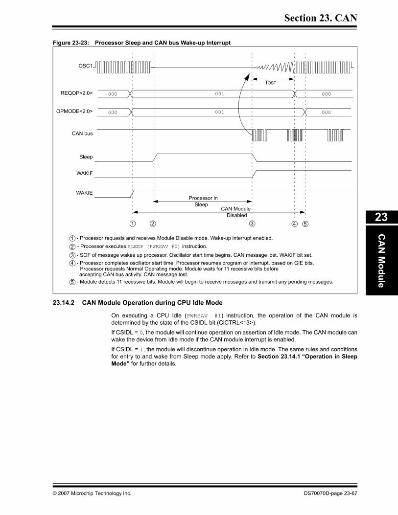
Section 23. CANC
AN
Module
23
Figure 23-23: Processor Sleep and CAN bus Wake-up Interrupt
23.14.2 CAN Module Operation during CPU Idle Mode
On executing a CPU Idle (PWRSAV #1) instruction, the operation of the CAN module isdetermined by the state of the CSIDL bit (CiCTRL<13>).
If CSIDL = 0, the module will continue operation on assertion of Idle mode. The CAN module canwake the device from Idle mode if the CAN module interrupt is enabled.
If CSIDL = 1, the module will discontinue operation in Idle mode. The same rules and conditionsfor entry to and wake from Sleep mode apply. Refer to Section 23.14.1 “Operation in SleepMode” for further details.
TOST
Processor inSleep
2 3 4 5
- Processor executes SLEEP (PWRSAV #0) instruction.
- SOF of message wakes up processor. Oscillator start time begins. CAN message lost. WAKIF bit set. - Processor completes oscillator start time. Processor resumes program or interrupt, based on GIE bits.
accepting CAN bus activity. CAN message lost. - Module detects 11 recessive bits. Module will begin to receive messages and transmit any pending messages.
OSC1
CAN bus
CAN ModuleDisabled
001
001000
000 000
000
Sleep
WAKIF
WAKIE
1
- Processor requests and receives Module Disable mode. Wake-up interrupt enabled.
Processor requests Normal Operating mode. Module waits for 11 recessive bits before
1234
5
REQOP<2:0>
OPMODE<2:0>
© 2007 Microchip Technology Inc. DS70070D-page 23-67

dsPIC30F Family Reference Manual
23.15 CAN Protocol OverviewThe Controller Area Network (CAN) is a serial communications protocol which efficientlysupports distributed real-time control with a very high level of robustness. The CAN Protocol isfully defined by Robert Bosch GmbH, in the CAN Specification V2.0B from 1991.
Its domain of application ranges from high speed networks to low cost multiplex wiring.Automotive electronics (i.e., engine control units, sensors, anti-skid-systems and so on) areconnected using CAN with bit rates up to 1 Mbit/sec. The CAN Network allows a cost effectivereplacement of wiring harnesses in the automobile. The robustness of the bus in noisyenvironments and the ability to detect and recover from fault conditions makes the bus suitablefor industrial control applications such as DeviceNet, SDS and other field bus protocols.
CAN is an asynchronous serial bus system with one logical bus line. It has an open, linear busstructure with equal bus nodes. A CAN bus consists of two or more nodes. The number of nodeson the bus may be changed dynamically without disturbing the communication of other nodes.This allows easy connection and disconnection of bus nodes (e.g., for addition of systemfunction, error recovery or bus monitoring).
The bus logic corresponds to a “wired-AND” mechanism, “recessive” bits (mostly, but notnecessarily equivalent to the logic level ‘1’) are overwritten by “dominant” bits (mostly logiclevel ‘0’). As long as no bus node is sending a dominant bit, the bus line is in the recessive state,but a dominant bit from any bus node generates the dominant bus state. Therefore, for the CANbus line, a medium must be chosen that is able to transmit the two possible bit states (dominantand recessive). One of the most common and cost effective ways is to use a twisted wire pair.The bus lines are then called “CANH” and “CANL”, and may be connected directly to the nodes,or via a connector. There is no standard defined by CAN regarding connector requirements. Thetwisted wire pair is terminated by terminating resistors at each end of the bus line. The maximumbus speed is 1 Mbit, which can be achieved with a bus length of up to 40 meters. For bus lengthslonger than 40 meters, the bus speed must be reduced (a 1000 m bus can be realized with a40 Kb bus speed). For bus lengths above 1000 meters, special drivers should be used. At least20 nodes may be connected without additional equipment. Due to the differential nature oftransmission, CAN is not inherently susceptible to radiated electromagnetic energy because bothbus lines are affected in the same way, which leaves the differential signal unaffected. The buslines may also be shielded to reduce the radiated electromagnetic emission from the bus itself,especially at high baud rates.
The binary data is coded corresponding to the NRZ code (Non-Return-to-Zero;low level = dominant state; high level = recessive state). To ensure clock synchronization of allbus nodes, bit-stuffing is used. This means that during the transmission of a message, amaximum of five consecutive bits may have the same polarity. Whenever five consecutive bits ofthe same polarity have been transmitted, the transmitter will insert one additional bit of theopposite polarity into the bit stream before transmitting further bits. The receiver also checks thenumber of bits with the same polarity and removes the stuff bits from the bit stream (destuffing).
In the CAN protocol, it is not bus nodes that are addressed. The address information is containedin the messages that are transmitted. This is done via an identifier (part of each message) whichidentifies the message content (e.g., engine speed, oil temperature etc.). This identifier alsoindicates the priority of the message. The lower the binary value of the identifier, the higher thepriority of the message.
For bus arbitration, Carrier Sense Multiple Access/Collision Detection (CSMA/CD) withNon-Destructive Arbitration (NDA) is used. If bus node A wants to transmit a message across thenetwork, it first checks that the bus is in the Idle state (“Carrier Sense”), (i.e., no node is currentlytransmitting). If this is the case (and no other node wishes to start a transmission at the samemoment), node A becomes the bus master and sends its message. All other nodes switch toReceive mode during the first transmitted bit (Start-Of-Frame bit). After correct reception of themessage (which is Acknowledged by each node), each bus node checks the message identifierand stores the message, if required. Otherwise, the message is discarded.
DS70070D-page 23-68 © 2007 Microchip Technology Inc.

Section 23. CANC
AN
Module
23
If two or more bus nodes start their transmission at the same time (“Multiple Access”), collisionof the messages is avoided by bitwise arbitration (“Collision Detection/Non-DestructiveArbitration” together with the “Wired-AND” mechanism, “dominant” bits override “recessive” bits).Each node sends the bits of its message identifier (Most Significant bit first) and monitors the buslevel. A node that sends a recessive identifier bit but reads back a dominant one loses busarbitration and switches to Receive mode. This condition occurs when the message identifier ofa competing node has a lower binary value (dominant state = logic 0) and therefore, thecompeting node is sending a message with a higher priority. In this way, the bus node with thehighest priority message wins arbitration without losing time by having to repeat the message.All other nodes automatically try to repeat their transmission once the bus returns to the Idlestate. It is not permitted for different nodes to send messages with the same identifier, asarbitration could fail, leading to collisions and errors later in the message.
The original CAN specifications (Versions 1.0, 1.2 and 2.0A) defined the message identifier ashaving a length of 11 bits giving a possible 2048 message identifiers. The specification has sincebeen updated (to version 2.0B) to remove this limitation. CAN specification Version 2.0B allowsmessage identifier lengths of 11 and/or 29 bits to be used (an identifier length of 29 bits allowsover 536 million message identifiers). Version 2.0B CAN is also referred to as “Extended CAN”;and Versions 1.0, 1.2 and 2.0A) are referred to as “Standard CAN”.
23.15.1 Standard CAN vs. Extended CAN
Those data frames and remote frames, which only contain the 11-bit identifier, are calledstandard frames according to CAN specification V2.0A. With these frames, 2048 differentmessages can be identified (identifiers 0-2047). However, the 16 messages with the lowestpriority (2032-2047) are reserved. Extended frames according to CAN specification V2.0B havea 29-bit identifier. As already mentioned, this 29-bit identifier is made up of the 11-bit identifier(“Standard lD”) and the 18-bit Extended identifier (“Extended ID”).
CAN modules specified by CAN V2.0A are only able to transmit and receive standard framesaccording to the Standard CAN protocol. Messages using the 29-bit identifier cause errors. If adevice is specified by CAN V2.0B, there is one more distinction. Modules named “Part B Passive”can only transmit and receive standard frames but tolerate extended frames without generatingerror frames. “Part B Active” devices are able to transmit and receive both standard andextended frames.
23.15.2 ISO Model
The lSO/OSl Reference Model is used to define the layers of protocol of a communication systemas shown in Figure 23-24. At the highest end, the applications need to communicate betweeneach other. At the lowest end, some physical medium is used to provide electrical signaling.
The higher levels of the protocol are run by software. Within the CAN bus specification, there isno definition of the type of message, or the contents, or meaning of the messages transferred.These definitions are made in systems such as Volcano, the Volvo automotive CAN specificationJ1939, the U.S. heavy truck multiplex wiring specification; and Allen-Bradley DeviceNet andHoneywell SDS, industrial protocols.
The CAN bus module definition encompasses two levels of the overall protocol:
• The Data Link Layer- The Logical Link Control (LLC) sub layer- The Medium Access Control (MAC) sub layer
• The Physical Layer- The Physical Signaling (PLS) sub layer
© 2007 Microchip Technology Inc. DS70070D-page 23-69

dsPIC30F Family Reference Manual
The LLC sub layer is concerned with Message Filtering, Overload Notification and ErrorRecovery Management. The scope of the LLC sub layer is:
• To provide services for data transfer and for remote data request.• To decide which messages received by the LLC sub layer are actually to be accepted.• To provide means for error recovery management and overload notifications.
The MAC sub layer represents the kernel of the CAN protocol. The MAC sub layer defines thetransfer protocol, (i.e., controlling the Framing, Performing Arbitration, Error Checking, ErrorSignalling and Fault Confinement). It presents messages received from the LLC sub layer andaccepts messages to be transmitted to the LLC sub layer. Within the MAC sub layer is where it’sdecided whether the bus is free for starting a new transmission, or whether a reception is juststarting. The MAC sub layer is supervised by a management entity called Fault Confinementwhich is a self-checking mechanism for distinguishing short disturbances from permanentfailures. Also, some general features of the bit timing are regarded as part of the MAC sub layer.
The physical layer defines the actual transfer of the bits between the different nodes with respectto all electrical properties. The PLS sub layer defines how signals are actually transmitted andtherefore deals with the description of Bit Timing, Bit Encoding and Synchronization.
The lower levels of the protocol are implemented in driver/receiver chips and the actual interfacesuch as twisted pair wiring or optical fiber and so on. Within one network, the physical layer hasto be the same for all nodes. The driver/receiver characteristics of the physical layer are notdefined in the CAN specification so as to allow transmission medium and signal levelimplementations to be optimized for their application. The most common example of the physicaltransmission medium is defined in Road Vehicles ISO11898, a multiplex wiring specification.
DS70070D-page 23-70 © 2007 Microchip Technology Inc.

Section 23. CANC
AN
Module
23
Figure 23-24: CAN Bus in ISO/OSI Reference Model
OSI REFERENCE LAYERS
Presentation
Transport
Data Link Layer
LLC (Logical Link Control)Acceptance FilteringOverload NotificationRecovery Management
MAC (Medium Access Control)Data Encapsulation/DecapsulationFrame Coding (stuffing, destuffing)Medium Access ManagementError DetectionError SignallingAcknowledgmentSerialization/Deserialization
Physical Layer
PLS (Physical Signalling)Bit Encoding/DecodingBit TimingSynchronization
PMA (Physical Medium Attachment)Driver/Receiver Characteristics
MDI (Medium Dependent Interface)Connectors
FaultConfinement
Bus FailureManagement
Supervisor
Shaded RegionsImplemented by the CAN Module
Has to be Implemented in dsPIC30F Firmware
Session
Network
Application
CANTransceiver
ChipConnector
© 2007 Microchip Technology Inc. DS70070D-page 23-71

dsPIC30F Family Reference Manual
23.16 Related Application NotesThis section lists application notes that are related to this section of the manual. Theseapplication notes may not be written specifically for the dsPIC30F Product Family, but theconcepts are pertinent and could be used with modification and possible limitations. The currentapplication notes related to the CAN module are:
Title Application Note #An Introduction to the CAN Protocol AN713
Note: Please visit the Microchip web site (www.microchip.com) for additional ApplicationNotes and code examples for the dsPIC30F Family of devices.
DS70070D-page 23-72 © 2007 Microchip Technology Inc.

Section 23. CANC
AN
Module
23
23.17 Revision HistoryRevision A This is the initial released revision of this document.
Revision BThis revision incorporates additional technical content for the dsPIC30F CAN module.
Revision CThis revision incorporates all known errata at the time of this document update.
Revision DThis revision incorporates changes to Example 23-1: “Bit Rate Calculation Example” andFigure 23-2: “CAN Buffers and Protocol Engine Block Diagram” as well as minor changesto the document text.
© 2007 Microchip Technology Inc. DS70070D-page 23-73

dsPIC30F Family Reference Manual
NOTES:
DS70070D-page 23-74 © 2007 Microchip Technology Inc.