
Seating EE 330 Spring 2018 Monte Grant Anaelclass.ece.iastate.edu/ee330/lectures/EE 330 Lect 15...
33
1 2 5 6 3 4 8 1 2 3 4 5 6 ROW Samuel Willford Kenneth Wendt Tyler Schurk Alvin Rymash Charles Rigsby Yao-Wei Lee Lingkai Lang Brian Kirkpatrick Jacob Gosse Christopher Goodrich Matthew Goetzman Leo Freier Grant Duncan Timothy Day Zaran Claes Ritika Chakravarty Alex Carpenter Kevin Carlson Zachary Bumstead Jacob Brown William Brandt Adithya Basnayake Kevin Angeliu Derek Nash Cassandra Plata Pengyu Qu Mitchell Hagar Brendon McGehee Matt Strong 7 Fengnan Yang Yimin Wang David Schmadeke Grant Larson Hamish Hay Monte Friestad Abuhjar Ahmed Jiaxin Li Nicholas Parsons Aboullah Al Obaidi 7 8 Jonathan Hugen Omar Elsherbiny Yao Cheah Mir Ahbab Anael Perruchoud Seating EE 330 Spring 2018
Transcript of Seating EE 330 Spring 2018 Monte Grant Anaelclass.ece.iastate.edu/ee330/lectures/EE 330 Lect 15...

1 2 5 63 4
8
1
2
3
4
5
6
RO
W
Samuel Willford
Kenneth Wendt
TylerSchurk
AlvinRymash
Charles Rigsby
Yao-Wei Lee
Lingkai Lang
Brian Kirkpatrick
Jacob Gosse
Christopher Goodrich
Matthew Goetzman
Leo Freier
Grant Duncan
Timothy Day
Zaran Claes
Ritika Chakravarty
Alex Carpenter
Kevin Carlson
Zachary Bumstead
Jacob Brown
William Brandt
Adithya Basnayake
Kevin Angeliu
Derek Nash
Cassandra Plata
Pengyu Qu
Mitchell Hagar
Brendon McGehee
Matt
Strong
7
Fengnan Yang
Yimin Wang
David Schmadeke
Grant Larson
Hamish Hay
Monte Friestad
Abuhjar Ahmed
Jiaxin Li
NicholasParsons
Aboullah Al Obaidi
7 8
Jonathan Hugen
Omar Elsherbiny
Yao Cheah
Mir Ahbab
Anael Perruchoud
Seating EE 330 Spring 2018

Reminder: Exam 1 Friday Feb 16
Students may bring one page of notes (front and back) but no electronic data storage or remote access
HW Assignment due on Wed of next week at end of class period (no late HW accepted)
Review session: Thursday Feb 15 6:00 p.m.Rm 1016 Coover

EE 330Lecture 15
Devices in Semiconductor Processes
• MOSFETs

Use of Piecewise Models for Nonlinear Devices when
Analyzing Electronic Circuits
Process:
1. Guess state of the device
2. Analyze circuit
3. Verify State
4. Repeat steps 1 to 3 if verification fails
Observations:
o Analysis generally simplified dramatically (particularly if piecewise model is linear)
o Approach applicable to wide variety of nonlinear deviceso Closed-form solutions give insight into performance of circuito Usually much faster than solving the nonlinear circuit directlyo Wrong guesses in the state of the device do not compromise solution
(verification will fail)
o Helps to Guess Right the first time
Review from Last Lecture

Basic Devices and Device Models
• Resistor
• Diode
• Capacitor
• MOSFET
• BJT
Review from Last Lecture

n-Channel MOSFET Operation and Model
VBS
VGS
VDS
ID=0
IG=0
IB=0
IDIG
IB
Model in Cutoff Region
Review from Last Lecture

n-Channel MOSFET Operation and Model
VBS
VGS
VDS
Increase VGS more
IDRCH=VDS
IG=0
IB=0
Inversion layer forms in channel
IDIG
IB
(VDS and VBS small)
Inversion layer will support current flow from D to S
Channel behaves as thin-film resistor
Critical value of
VGS that creates
inversion layer
termed threshold
voltage, VT)
Review from Last Lecture

Triode Region of Operation
OXTGS
CHCVV
1
W
LR
0II
VVVL
WμCI
BG
DSTGSOXD
For VDS small
VDS
VBS = 0
VGS
ID
IG
IB
VDSRCH
Behaves as a resistor between
drain and source
Model in Deep Triode Region
Review from Last Lecture

Triode Region of Operation
OXTGS
CHCVV
1
W
LR
For VDS small
VBS = 0
VGS
ID
IG
IB
RCH
Resistor is controlled by the voltage VGS
Termed a “Voltage Controlled Resistor” (VCR)
Review from Last Lecture
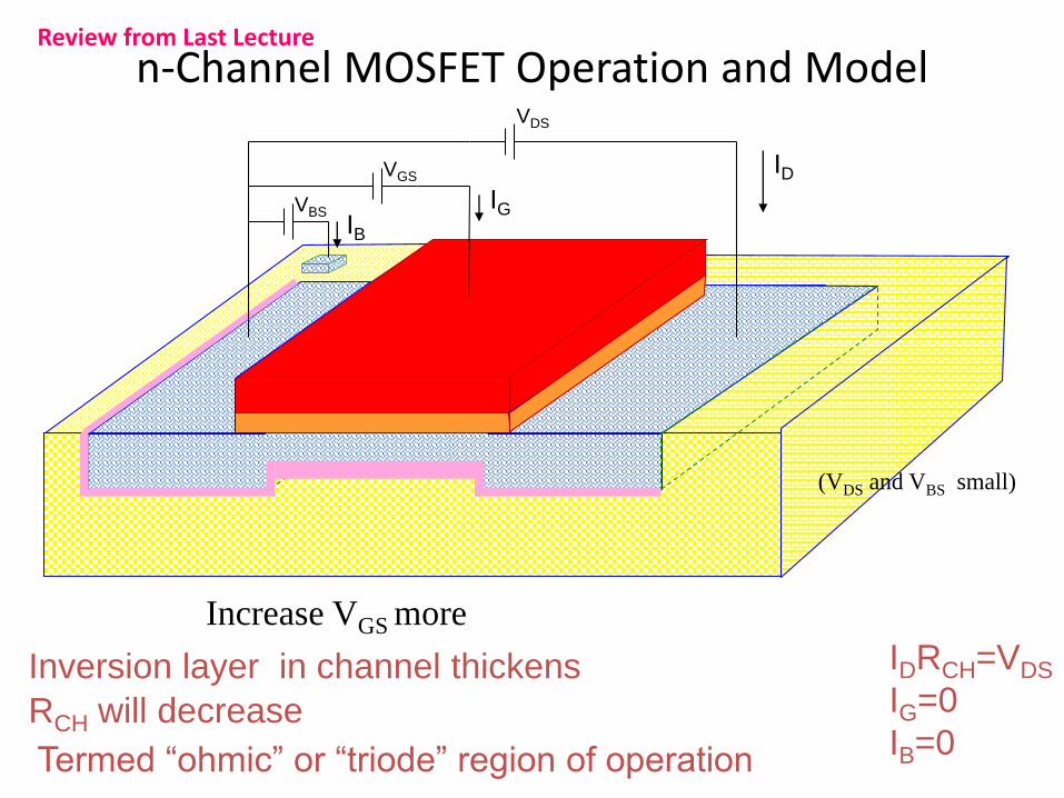
n-Channel MOSFET Operation and Model
VBS
VGS
VDS
Increase VGS more
IDRCH=VDS
IG=0
IB=0
Inversion layer in channel thickens
IDIG
IB
(VDS and VBS small)
RCH will decrease
Termed “ohmic” or “triode” region of operation
Review from Last Lecture
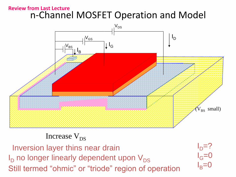
n-Channel MOSFET Operation and Model
VBS
VGS
VDS
Increase VDS
ID=?
IG=0
IB=0
Inversion layer thins near drain
IDIG
IB
(VBS small)
ID no longer linearly dependent upon VDS
Still termed “ohmic” or “triode” region of operation
Review from Last Lecture

Triode Region of Operation
VDS
VBS = 0
VGS
ID
IG
IB
OXTGS
CHCVV
1
W
LR
0II
V2
VVV
L
WμCI
BG
DSDS
TGSOXD
For VDS larger
Model in Triode Region
Review from Last Lecture

n-Channel MOSFET Operation and Model
VBS
VGS
VDS
Increase VDS even more
ID=?
IG=0
IB=0
Inversion layer disappears near drain
IDIG
IB
(VBS small)
Termed “saturation”region of operation
Saturation first occurs when VDS=VGS-VT

Saturation Region of Operation
VDS
VBS = 0
VGS
ID
IG
IB
0II
VV2L
WμCI
VV2
VVVV
L
WμCI
V2
VVV
L
WμCI
BG
2
TGSOX
D
TGSTGS
TGSOXD
DSDS
TGSOXD
lyequivalentor
lyequivalentorFor VDS at onset of
saturation

n-Channel MOSFET Operation and Model
VBS
VGS
VDS
Increase VDS even more (beyond VGS-VT)
ID=?
IG=0
IB=0
Nothing much changes !!
IDIG
IB
(VBS small)
Termed “saturation”region of operation

Saturation Region of Operation
VDS
VBS = 0
VGS
ID
IG
IB
0II
VV2L
WμCI
BG
2
TGSOX
D
For VDS in Saturation
Model in Saturation Region

Model SummaryVDS
VBS = 0
VGS
ID
IG
IB
GS T
DSD OX GS T DS GS DS GS T
2
OX GS T GS T DS GS T
G B
0 V V
VWI μC V V V V V V V V
L 2
WμC V V V V V V V
2L
I =I =0
T
Note: This is the third model we have introduced for the MOSFET
Cutoff
Triode
Saturation
OXTGS
CHCVV
1
W
LR
(Deep triode special case of triode where VDS is small )
This is a piecewise model (not piecewise linear though)

Model Summary
VDS
VBS = 0
VGS
ID
IG
IBVBS
TGSDSTGS
2
TGSOX
TGSDSGSDSDS
TGSOX
TGS
D
VVVVVVV2L
WμC
VVVVVV2
VVV
L
WμC
VV0
I T
Observations about this model (developed for VBS=0):
D 1 GS DS
G 2 GS DS
B 3 GS DS
I = f V ,V
I = f V ,V
I = f V ,V
This is a nonlinear model characterized by the functions f1, f2, and f3 where
we have assumed that the port voltages VGS and VDS are the independent
variables and the drain currents are the dependent variables
G BI = I = 0

General Nonlinear Model
1 1 1 2
2 2 1 2
I = f V ,V
I = f V ,V
I1 and I2 are 3-dimensional relationships which are often difficult to visualize
v1 v2
I1 I23-terminal
Nonlinear
Device
Two-dimensional representation of 3-dimensional relationships

Graphical Representation of MOS Model
GS T
DS
D OX GS T DS GS DS GS T
2
OX GS T GS T DS GS T
0 V V
VWI μC V V V V V V V V
L 2
WμC V V V V V V V
2L
T
G BI =I =0
0
0.5
1
1.5
2
2.5
3
0 1 2 3 4 5
VDS
Cutoff
Triode
Saturation
ID
VDS
VGS1
VGS2
VGS3
VGS4
Deep Triode
RegionRegion
2
DSD OX
VWI =μC
L 2

PMOS and NMOS Models
S
D
G
0
0.5
1
1.5
2
2.5
3
0 1 2 3 4 5
VDS
Cutoff
Triode
Saturation
ID
VDS
2
D OX DS
WI = μC V
L
VGS1
VGS2
VGS3
VGS4
Deep Triode
RegionRegion
D
S
G
• Functional form identical, sign changes and parameter values different• Will give details about p-channel model later

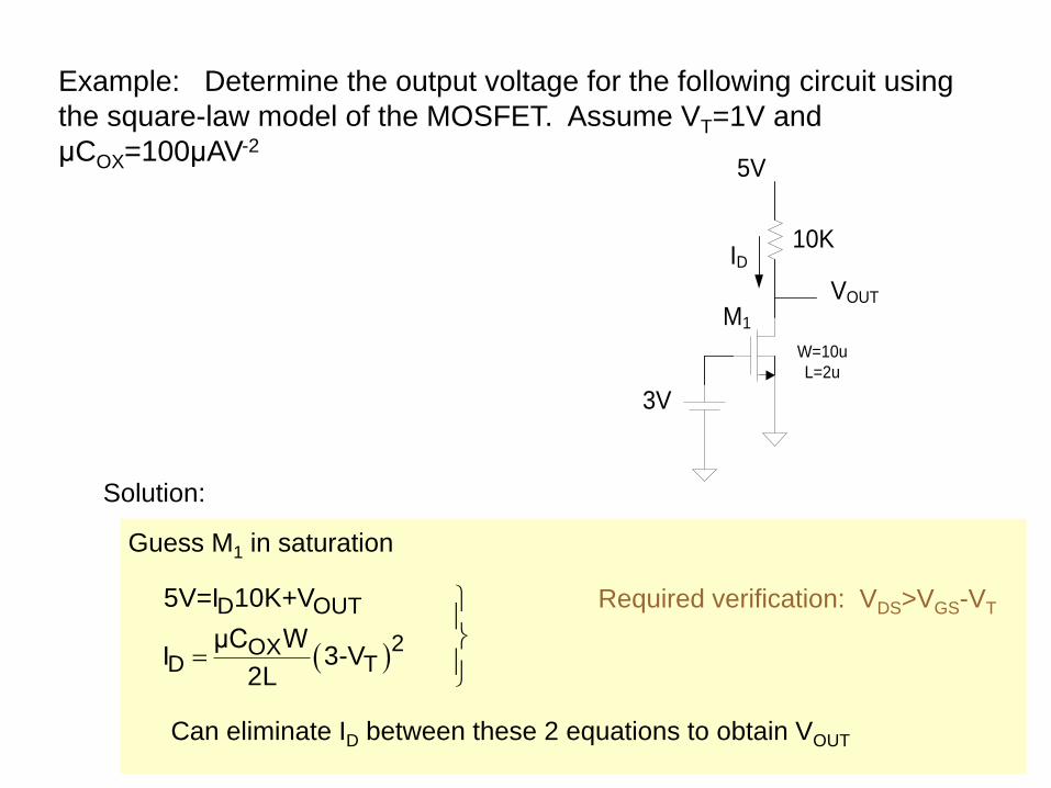
Example: Determine the output voltage for the following circuit using
the square-law model of the MOSFET. Assume VT=1V and
μCOX=100μAV-2
Solution:
Since VGS>VT, M1 is operating in either saturation or triode region
10K
W=10u
L=2u
5V
3V
VOUT
M1
ID
Strategy will be to guess region of operation, solve, and then verify region
Example: Determine the output voltage for the following circuit using
the square-law model of the MOSFET. Assume VT=1V and
μCOX=100μAV-2
Solution:
10K
W=10u
L=2u
5V
3V
VOUT
M1
ID
Guess M1 in saturation
D OUT
2OXD T
5V=I 10K+V
μC WI 3-V
2L
Required verification: VDS>VGS-VT
Can eliminate ID between these 2 equations to obtain VOUT

Example: Determine the output voltage for the following circuit using
the square-law model of the MOSFET. Assume VT=1V and
μCOX=100μAV-2
10K
W=10u
L=2u
5V
3V
VOUT
M1
IDGuess M1 in saturation
D OUT
2OXD T
5V=I 10K+V
μC WI 3-V
2L
Required verification: VDS>VGS-VT
2-2
OUT100μAV 10
V = 5V-10K 2V2 2
2-2
OUT100μAV 10
V = 5V-10K 2V2 2
OUTV = -5V
Verification: VDS=VOUT
-5 >? 2V - - 0 No! So verification fails and Guess of region is invalid

Example: Determine the output voltage for the following circuit using
the square-law model of the MOSFET. Assume VT=1V and
μCOX=100μAV-2
10K
W=10u
L=2u
5V
3V
VOUT
M1
IDGuess M1 in triode
D OUT
OX DSD T DS
5V=I 10K+V
μC W VI 3-V V
L 2
Required verification: VDS<VGS-VT
-2OUT
OUT OUTV100μAV 10
V = 5V-10K 2V- V2 2
OUTV = 0.515V
Verification: VDS=VOUT
0.515 <? 2V - - 0 Yes! So verification succeeds and triode region is valid
OUTOUT OUT
VV = 5V- 5 2V- V
2
Solving for VOUT, obtain
OUTV = 0.515V

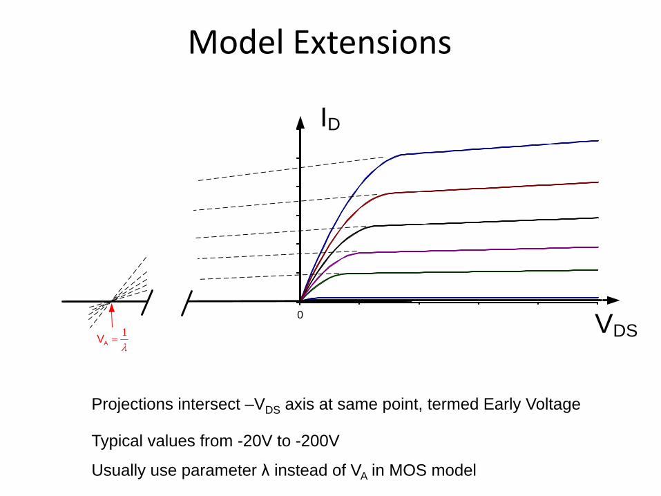
Model Extensions
0
50
100
150
200
250
300
0 1 2 3 4 5
1AV
VDS
ID
Projections intersect –VDS axis at same point, termed Early Voltage
Typical values from -20V to -200V
Usually use parameter λ instead of VA in MOS model

VDD
VIN VOUT
VIN
VDD
VDD
VOUT
VIN
VDD
VOUT
? ?
Switch-Level Models Simple square-law Model
VDD
VIN
VOUT
VBIAS
Logic Gate
Voltage Amplifier
Switch-Level Models
Simple square-law Model?Voltage Gain
Input/Output Relationship}
Limitations of Existing Models
Model Extensions
0
50
100
150
200
250
300
0 1 2 3 4 5
1AV
VDS
ID
Projections intersect –VDS axis at same point, termed Early Voltage
Typical values from -20V to -200V
Usually use parameter λ instead of VA in MOS model

Model Extensions
0
50
100
150
200
250
300
0 1 2 3 4 5
Vds
Id
0
50
100
150
200
250
300
0 1 2 3 4 5
Vds
Id
Existing Model
Actual Device
Slope is not 0

Model Extensions
0
50
100
150
200
250
300
0 1 2 3 4 5
Vds
Id
TGSDSTGSDS
2
TGSOX
TGSDSGSDSDS
TGSOX
TGS
D
VVVVVVVV2L
WμC
VVVVVV2
VVV
L
WμC
VV0
I
1
T
Note: This introduces small discontinuity (not shown) in model at SAT/Triode transition

Further Model Extensions
Existing model does not depend upon the bulk voltage !
Observe that changing the bulk voltage will change the electric field in the
channel region !
VBS
VGS
VDS
IDIG
IB
(VBS small)
E


End of Lecture 15


![EE 330 Lecture 42 - Iowa State Universityclass.ece.iastate.edu/ee330/lectures/EE 330 Lect 42 Fall 2016.pdf · EE 330 Lecture 42 Digital Circuits • Elmore Delay ... Elmore delay[1]](https://static.fdocuments.us/doc/165x107/5b57fe847f8b9a4e1b8b664d/ee-330-lecture-42-iowa-state-330-lect-42-fall-2016pdf-ee-330-lecture-42-digital.jpg)

