SD Express and microSD Express Memory Cards: The Best ... · 3 SD Express Cards and microSD Express...
11
1 SD Express Cards and microSD Express Memory Cards – The Best Choice for Your Future Product Designs White Paper www.sdcard.org | ©2019 SD Association. All rights reserved SD Express and microSD Express Memory Cards: The Best Choice for Your Future Product Designs White Paper | February 2019
Transcript of SD Express and microSD Express Memory Cards: The Best ... · 3 SD Express Cards and microSD Express...
1SD Express Cards and microSD Express Memory Cards – The Best Choice for Your Future Product Designs White Paper
www.sdcard.org | ©2019 SD Association. All rights reserved
SD Express and microSD Express Memory Cards: The Best Choice for Your Future Product Designs
White Paper | February 2019

Conditions for publication
Publisher and Copyright Holder:
SD Card Association2400 Camino Ramon, Suite 375San Ramon, CA 94583 USATelephone: +1 (925) 275-6615Fax: +1 (925) 886-4870E-mail: [email protected]
Disclaimers:
The information contained in this white paper is provided as is without any representations or warranties of any kind. No responsibility is assumed by the SD Association for any damages, or any infringements of patents or other rights of the SD Association or any third-parties, which may result from the use of any portion thereof. No license is granted by implication, estoppel or otherwise under any patent or other rights of the SD Association or any third-party. Nothing herein shall be construed as an obligation by the SD Association to disclose or distribute any technical information, know-how or other confidential information to any third party.
Trademarks Notice:
SD and related marks and logos are trademarks of SD-3C LLC.
© 2019 SD-3C LLC. All Rights Reserved.
Linux® is registered trademark of Linus Torvalds.
eMMC, UFS and UFS Card specifications originated by JEDEC
SATA (Serial ATA) is a specification originated by Serial ATA International Organization (SATA-IO) which is owned today and driven by INCITS T13 and T10 (SCSI)
PCI Express® is a registered trademark of PCI-SIG®.
NVM ExpressTM and NVMeTM are trademarks of NVM Express, Inc.
2SD Express Cards and microSD Express Memory Cards – The Best Choice for Your Future Product Designs White Paper
www.sdcard.org | ©2019 SD Association. All rights reserved

3SD Express Cards and microSD Express Memory Cards – The Best Choice for Your Future Product Designs White Paper
www.sdcard.org | ©2019 SD Association. All rights reserved
Executive Summary
This white paper explains how the features of microSD Express card - the microSD card that includes the widely used SD interface along with the most advanced memory interface protocols of PCIe® and NVMe™ – brings the favorite SD standard to new SSD levels of performance enabling exceptional new user experience for multi-processing environments.
This paper highlights the advantages of the new microSD Express by comparing it with similar standards in the market. This information should make a compelling case for host OEMs to adopt the SD Express or microSD Express interface in their future products.
SD and PCIe/NVMe Standards
The SD Association (SDA) introduced the first SD memory cards almost 20 years ago. The SD memory card standard, along with the microSD memory card, evolved during the last two decades as our world, devices and storage changed in unimaginable ways. SD memory cards relying on the SD specifications are sold in billions each year. The SDA gained enormous experience after 20 years in the complex consumer market with its many different needs.
PCIe and NVMe standards are developed by PCI SIG and NVM Express respectively. PCIe has been adapted for a wide array of use cases and has become one of the most popular interfaces for PCs, mobile computing, phones, gaming, cameras, automotive, to name a few. The combination of PCIe with NVMe has gained favor as de-facto standards, replacing the older ATA and SCSI command layers, and are on a path to become the leading technology of most non-volatile memory interfaces.
Combining the vast experience of the SDA and its two renowned form factors, SD and microSD, with the globally proven standards of PCIe and NVMe, created the revolutionary SD Express and microSD Express specification.
In addition to the performance advancements, SD Express maintains the long-standing advantage of SD: backward compatibility and interoperability. The PCIe interface was added in addition to the existing SD (UHS-I) interface, allowing a card with SD Express to operate interchangeably in new SD Express capable hosts as well as billions of existing SD host products in the market today.
Figure 1 SD Express - A Combination of Three Leading Standards

Figure 2 SD Express – The best from all worlds
Integration of PCIe and NVMe into SD brings reliable, proven and globally recognized standards full of features that are optimized to various market applications and advanced flash memory technologies. This means that SD now benefits from these two standards’ continued research, development and long term roadmaps that will ignite the imagination of SD and microSD memory card users.
The growing need for faster protocols
The initial SD Express and microSD Express specifications are based on a single channel of PCIe 3.1 interface that allows bandwidth of up to 985MB/s. Adoption of the PCIe interface puts SD on a path to adopt new PCI SIG standards, such as Gen4 with 2GB/s and Gen 5 with 4GB/s.
Faster speeds are essential for high performance content applications such as: speed hungry applications running on cards and mobile computing devices, real memory expansion for mobile computing, ever-evolving gaming systems, multi-channel IoT devices, multi-processing automotive storage needs, high performance mobile phones, super-slow motion video, RAW continuous burst mode photography, 8K video capture and playback, 360 degree video, and any new applications that may enjoy from such a small removable memory cards with such advance high performance capabilities.
These applications, along with evolving technology trends, signal a clear demand for memory cards with high performance sequential and random access provided by SD Express.
4SD Express Cards and microSD Express Memory Cards – The Best Choice for Your Future Product Designs White Paper
www.sdcard.org | ©2019 SD Association. All rights reserved
Figure 3 PCIe Evolution Roadmap1
_____________
(1) PCIe DevConf 2018 Update
5
SD Express offers both a UHS-I interface and the PCIe/NVMe interface. The specification was defined in a way that the SD Express card may be initialized either through the legacy SD interface or directly through the PCIe/NVMe interface. If accessed through PCIe, the card introduces itself as Standard NVMe device. By relying on successful protocols already in the marketplace, the SDA gives the industry an advantage by leveraging existing test equipment and saving in product development processes. When companies use existing building blocks and existing designs, this translates to cost savings and an improved bottom line.
Plus, with existing support of major operating systems and popularity of drivers supporting PCIe/NVMe, the market adoption of SD Express is made easy.
Figures 4 and 5 shows the microSD Express and full size SD Express cards.
More detailed information on the SD Express and microSD Express interfaces and functionality may be found in the SD Express White Paper.
SD Express memory cards may consume up to maximum of 1.80 Watts from the host, representing the accumulated wattage from the two power supplies.
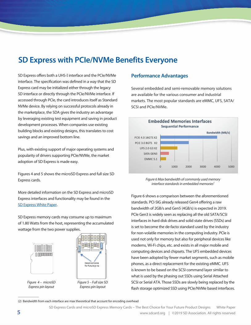
Performance Advantages
Several embedded and semi-removable memory solutions are available for the various consumer and industrial markets. The most popular standards are eMMC, UFS, SATA/ SCSI and PCIe/NVMe.
Figure 6 Max bandwidth of commonly used memoryinterface standards in embedded memories2
Figure 6 shows a comparison between the aforementioned standards. PCI-SIG already released Gen4 offering a raw bandwidth of 2GB/s and Gen5 (4GB/s) is expected in 2019. PCIe Gen3 is widely seen as replacing all the old SATA/SCSI interfaces in hard disk drives and solid state drives (SSDs) and is set to become the de-facto standard used by the industry for non-volatile memories in the computing industry. PCIe is used not only for memory but also for peripheral devices like modems, Wi-Fi chips, etc. and exists in all major mobile and computing devices and chipsets. The UFS embedded devices have been adopted by fewer market segments, such as mobile phones, as a direct replacement for the existing eMMC. UFSis known to be based on the SCSI command layer similar to what is used by the phasing out SSDs using Serial Attached SCSI or Serial ATA. Those SSDs are slowly being replaced by the flash storage optimized SSD using PCIe/NVMe based interfaces.
Figure 5 – Full size SD Express pin layout
Figure 4 – microSD Express pin layout
SD Express with PCIe/NVMe Benefits Everyone
SD Express Cards and microSD Express Memory Cards – The Best Choice for Your Future Product Designs White Paper
www.sdcard.org | ©2019 SD Association. All rights reserved
_____________
(2) Bandwidth from each interface are max theoretical that account for encoding overhead
6
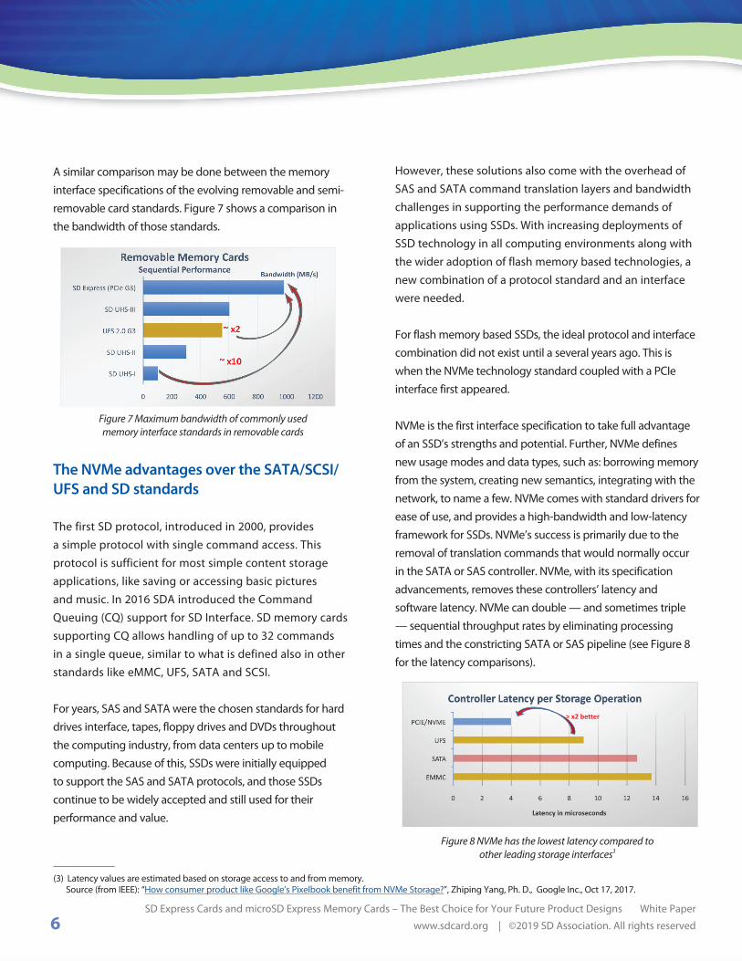
A similar comparison may be done between the memory interface specifications of the evolving removable and semi-removable card standards. Figure 7 shows a comparison in the bandwidth of those standards.
Figure 7 Maximum bandwidth of commonly usedmemory interface standards in removable cards
The NVMe advantages over the SATA/SCSI/UFS and SD standards
The first SD protocol, introduced in 2000, provides a simple protocol with single command access. This protocol is sufficient for most simple content storage applications, like saving or accessing basic pictures and music. In 2016 SDA introduced the Command Queuing (CQ) support for SD Interface. SD memory cards supporting CQ allows handling of up to 32 commands in a single queue, similar to what is defined also in other standards like eMMC, UFS, SATA and SCSI.
For years, SAS and SATA were the chosen standards for hard drives interface, tapes, floppy drives and DVDs throughout the computing industry, from data centers up to mobile computing. Because of this, SSDs were initially equipped to support the SAS and SATA protocols, and those SSDs continue to be widely accepted and still used for their performance and value.
However, these solutions also come with the overhead of SAS and SATA command translation layers and bandwidth challenges in supporting the performance demands of applications using SSDs. With increasing deployments of SSD technology in all computing environments along with the wider adoption of flash memory based technologies, a new combination of a protocol standard and an interface were needed.
For flash memory based SSDs, the ideal protocol and interface combination did not exist until a several years ago. This is when the NVMe technology standard coupled with a PCIe interface first appeared.
NVMe is the first interface specification to take full advantage of an SSD’s strengths and potential. Further, NVMe defines new usage modes and data types, such as: borrowing memory from the system, creating new semantics, integrating with the network, to name a few. NVMe comes with standard drivers for ease of use, and provides a high-bandwidth and low-latency framework for SSDs. NVMe’s success is primarily due to the removal of translation commands that would normally occur in the SATA or SAS controller. NVMe, with its specification advancements, removes these controllers’ latency and software latency. NVMe can double — and sometimes triple — sequential throughput rates by eliminating processing times and the constricting SATA or SAS pipeline (see Figure 8 for the latency comparisons).
Figure 8 NVMe has the lowest latency compared toother leading storage interfaces3
SD Express Cards and microSD Express Memory Cards – The Best Choice for Your Future Product Designs White Paper
www.sdcard.org | ©2019 SD Association. All rights reserved
_____________
(3) Latency values are estimated based on storage access to and from memory. Source (from IEEE): “How consumer product like Google’s Pixelbook benefit from NVMe Storage?”, Zhiping Yang, Ph. D., Google Inc., Oct 17, 2017.
>x2better

7
Another performance and scale feature of the NVMe is Multiple Queues, which support a large number of deep queues and commands per queue. Various studies4,5 show that NVMe based interface may achieve more than 30% improvement in random performance over SCSI based interfaces. These capabilities drove expanded NVMe adoption when hyperscale environments became popular. The same advantage may be utilized in any future multi-processing systems that are widely evolved in all market segments, including mobile devices. These new scale-out architectures mean NVMe has clear advantages in highly scalable deployments. The SCSI bottleneck of middle-layer translations struggled to support simultaneous IOs and multiple hosts, making SAS difficult to expand effectively. With Multitenant and Multiple Queues features, NVMe removes the bottleneck and seamlessly supports these environments.
The UFS specification developed by JEDEC uses the above-mentioned SCSI command layer with a few added new commands unique to UFS specification.
Figure 9 shows an example of how in a multi core system, NVMe can have a dedicated command queue in the DRAM for every CPU core while in other commonly used embedded or removable cards (ie UFS, eMMC and SD) there is a bottle neck of a single available queue supported by the host controller interface.
Adoption of the PCIe/NVMe in SD Express means adopting the protocols of the future. These protocols are expected to serve the memory interfacing ecosystem for the next decade and beyond.
SD Express Cards and microSD Express Memory Cards – The Best Choice for Your Future Product Designs White Paper
www.sdcard.org | ©2019 SD Association. All rights reserved
Figure 9 Host controller synchronization lock vsMulti Queue support of NVM
• Other legacy embedded memory interfaces, as well as UFS, have one command queue supported by the Host controller.
• Synchronization and locking are needed in legacy protocols to mutually access the single queue.
• Legacy interface’s host controller is a system bottleneck in the architecture.
_____________
(4) Source: Cisco, EMC Intel (@ SNIA presentation) https://docplayer.net/402021-The-performance-impact-of-nvme-and-nvme-over-fabrics.html
(5) Source: Micron. White paper from July 2018: “Comparing UFS and NVMeTM Storage Stack and System-Level Performance in Embedded Systems”
The PCIe Interface Advantages Advantages of the Differential Interface The legacy SD UHS-I interface have single ended type of signal lines, similar to eMMC. The PCIe Gen3 uses a differential interface of serial communication, similar to SD UHS-II and UFS. In addition, the PCIe interface used in SD Express uses only two side band signals (PERST# and CLKREQ#). There are several known benefits for differential interface:
Figure 10 Differential Interface Topology
8
• Resistance to Incoming EMI and Crosstalk When electromagnetic interference (EMI) or crosstalk is
generated by nearby signals, or introduced from outside the differential conductors, it is added equally to the inverted and non-inverted signal. The receiver responds to the difference in voltage between the two signals and not to the single-ended, ground-referenced voltage, and the receiver circuitry will greatly reduce the amplitude of the interference or crosstalk. Differential signals are less sensitive to EMI, crosstalk, and any other noise that couples into both signals of the differential pair.
• Reduction of Outgoing EMI and Crosstalk Rapid transitions, such as the rising and falling edges
of digital signals, can generate significant amounts of EMI. Both single-ended and differential signals generate EMI, but the two signals in a differential pair will create electromagnetic fields that are equal in magnitude, but opposite in polarity. This, in conjunction with techniques that maintain close proximity between the two conductors, or in case of cables using twisted-pair wires, ensures that the emissions from the two conductors will largely cancel each other out.
• Lower Signal-to-Noise Ratio (SNR) Differential signals can use lower voltages and still
maintain adequate SNR. The SNR of differential signaling is automatically increased by a factor of two, relative to an equivalent single-ended implementation because the dynamic range at the differential receiver is twice as high as the dynamic range of each signal within the differential pair.
• Simpler High/Low states detection In differential signals, determining the logic state is
straightforward. If the non-inverted signal’s voltage is higher than the inverted signal’s voltage, you have logic high. If the non-inverted voltage is lower than the inverted voltage, you have logic low. And the transition between the two states is the point at which the non-inverted and inverted signals intersect—i.e., the crossover point.
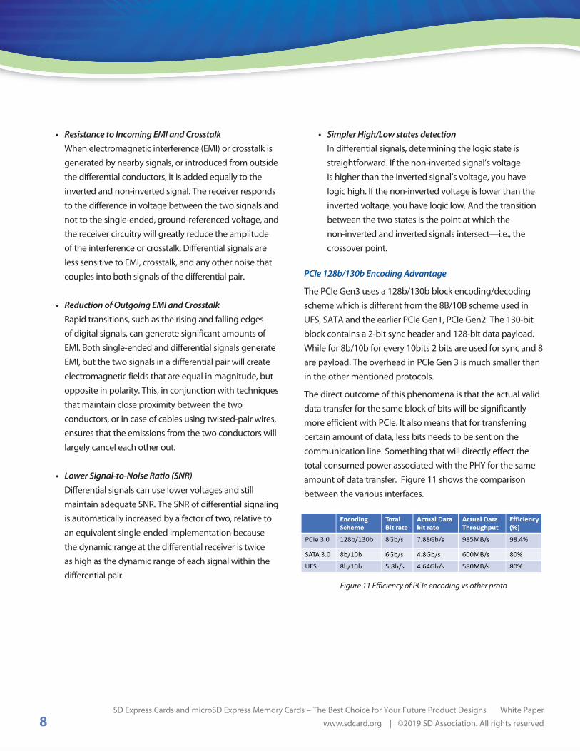
PCIe 128b/130b Encoding Advantage
The PCIe Gen3 uses a 128b/130b block encoding/decoding scheme which is different from the 8B/10B scheme used in UFS, SATA and the earlier PCIe Gen1, PCIe Gen2. The 130-bit block contains a 2-bit sync header and 128-bit data payload. While for 8b/10b for every 10bits 2 bits are used for sync and 8 are payload. The overhead in PCIe Gen 3 is much smaller than in the other mentioned protocols.
The direct outcome of this phenomena is that the actual valid data transfer for the same block of bits will be significantly more efficient with PCIe. It also means that for transferring certain amount of data, less bits needs to be sent on the communication line. Something that will directly effect the total consumed power associated with the PHY for the same amount of data transfer. Figure 11 shows the comparison between the various interfaces.
Figure 11 Efficiency of PCIe encoding vs other proto
SD Express Cards and microSD Express Memory Cards – The Best Choice for Your Future Product Designs White Paper
www.sdcard.org | ©2019 SD Association. All rights reserved

The Power Consumption Advantages
PCIe interface was originally introduced and used by PCs, servers, etc. The same PCIe concepts that were greatly improved by adding lower power sub-states and adoption of other mobile low power technologies, brought the PCIe to be fully competitive and capable of being used in mobile devices. PCIe 3.1, which was adopted by SD Express, includes the new low power sub-states L1.0, L1.1 and L1.2 that were added on top of L0 to L3 introduced earlier by PCIe 3.0. The new sub-states enabled additional low power states that allow for the best system optimization of low power vs recovery times. The fundamental idea behind L1 sub-states is to use something other than the high-speed logic inside the PCIe transceivers to wake the devices. The goal is to achieve near zero power consumption with an active state. That is achieved by adding additional functionality to an existing PCIe pin (CLKREQ#) to provide a simple signaling protocol. This allows the PCIe transceivers to turn off their high-speed circuits and rely on the new signaling to wake them up again. Both L1.1 and L1.2 permit the PCIe transceivers to turn off their PLLs along with their receivers and transmitters, while L1.2 even allows turning off the common mode keeper circuits (Figure 12).
Figure 12 PCIe 3.1 L1.x Low Power Sub-states
PCIe interfaces are widely used today in mobile equipment either for peripheral or memory interfacing.
For most applications, it was found that related to the PHY, the main power consuming factors are dependent on standby power, the power consumed in idle time. While the PHY itself is quite a low factor out of the total consumption in a full active system.
The legacy SD interface up to UHS-I consists of six single ended signals that may operate either in 3.3v or 1.8v logic levels. The 1.8v signaling allows lower power consumption verses the 3.3v. The differential interfaces introduced by SD UHS-II/III interface (0.14-0.28v) as well as the PCIe interface (0.25-1.2v), introduced with SD Express, allows significant lower voltage swing that reduce the consumed power contributed by the PHY during data transfer. Since the transfer rate is faster, the bottom line is that the new high speed interface will be much more energy efficient than legacy SD UHS-I interface. This is due to the fact that a system may transfer the same amount of data in shorter time and stay longer time in standby mode (see Figure 13).
Advantages of AC coupling over DC Coupling There are two commonly used interface coupling methods – AC and DC coupling. The PCIe physical interface has AC coupling. AC coupling provides many benefits, such as level shifting, removing common-mode errors, and protecting against input-voltage fault conditions. By using capacitors at the interface, the DC common mode voltage is isolated between the receiver and transmitter. Such isolation provides more stable and flexible system solutions that are less sensitive to noise, non-equal grounding, etc. Therefore, the PCIe interface has advantages mainly in connections between different units using connectors and cables, such as removable memory cards.
9
Performance of max 985MB/s (PCIe Gen3)
Pow
er c
onsu
mp�
on
Ac�ve Standby
Ac�ve Standby
Performance of max 104MB/s (SD UHS-I)
Pow
er c
onsu
mp�
on
SD Express Cards and microSD Express Memory Cards – The Best Choice for Your Future Product Designs White Paper
www.sdcard.org | ©2019 SD Association. All rights reserved
Figure 13 SD Express – Consumes Less Energy Power consumption of SD Express vs SD UHS-I for specific data transfer
10SD Express Cards and microSD Express Memory Cards – The Best Choice for Your Future Product Designs White Paper
www.sdcard.org | ©2019 SD Association. All rights reserved
Another advantage is found when the SD memory card socket is wired. Such solutions may be found in automotive, industrial applications, IoT and more. In automotive, the differential signals are always AC-coupled, protecting from overvoltage. Protecting the car’s battery voltage from shorts is the primary motivation for this configuration. A universal requirement for any signal entering the wiring harness is that it must withstand a short-to-battery voltage without damage. With an AC-coupled differential interface link, there is only a brief pulse of high current as the coupling capacitors are charged to the battery voltage. The peak amplitude of the current is a function of the actual impedance of the short. The duration of the current spike is a function of the coupling capacitance and the protection structure of the differential signal input and output. Operation can be restored once the short is removed. With SD Express, both AC coupling capacitors are placed on the host side. That allows application manufacturers to define the capacitors’ characteristics, such as max voltage, per system needs.
SD Express – Continuing the Promise of Full Backward Compatibility
SD memory cards have always kept backward compatibility as the basic functionality of its interface. Assurance of backward compatibility to users is one of the biggest strengths of all SD memory cards. Consumers that purchase cards know that they may remove the card and use it in another device. The card and device may not reach its best performance capability, but the consumer will gain access to all content. SD Express continues this long-standing promise by keeping the ability to operate the new cards in billions of existing products
available in the market through its legacy SD interface.
PCIe/NVMe is Supported by All Major Operating Systems
PCIe and NVMe are very popular in the industry and supported by all major market leaders. All major operating systems, Windows, MacOS, Linux and Android, support PCIe
and NVMe. Drivers are readily available, reducing the need to create extra drivers to support SD Express memory cards except the low-level driver required to control between the two available interfaces of SD and PCIe.
Tips for Host Product Manufacturers
With use of the PCIe/NVMe interface, host product manufacturers can now consider using existing SD interface and PCIe/NVMe building blocks to utilize the new SD Express host interface development.
The only challenge with this design is the switching mechanism and/or pullups/pulldown IO controls of the shared signals – REFCLK, CLKREQ# and PERST#. This IO control circuit may be quite simple; however, it requires understanding of both interfaces in each stage of the initialization process and normal operation of each of the two modes. An off-the-shelf solution for combining existing PCIe and SD interfaces on the host side may be found in the market.
SD Express test fixtures that serve as adapters to existing PCI SIG base board compliance as well as board for host testing are expected to be available soon by SDA or any of our approved test labs. Card and host manufacturers may use them in the test labs or in their own facilities and utilize existing PCIe/NVMe test equipment to perform compliance tests used by PCI SIG.
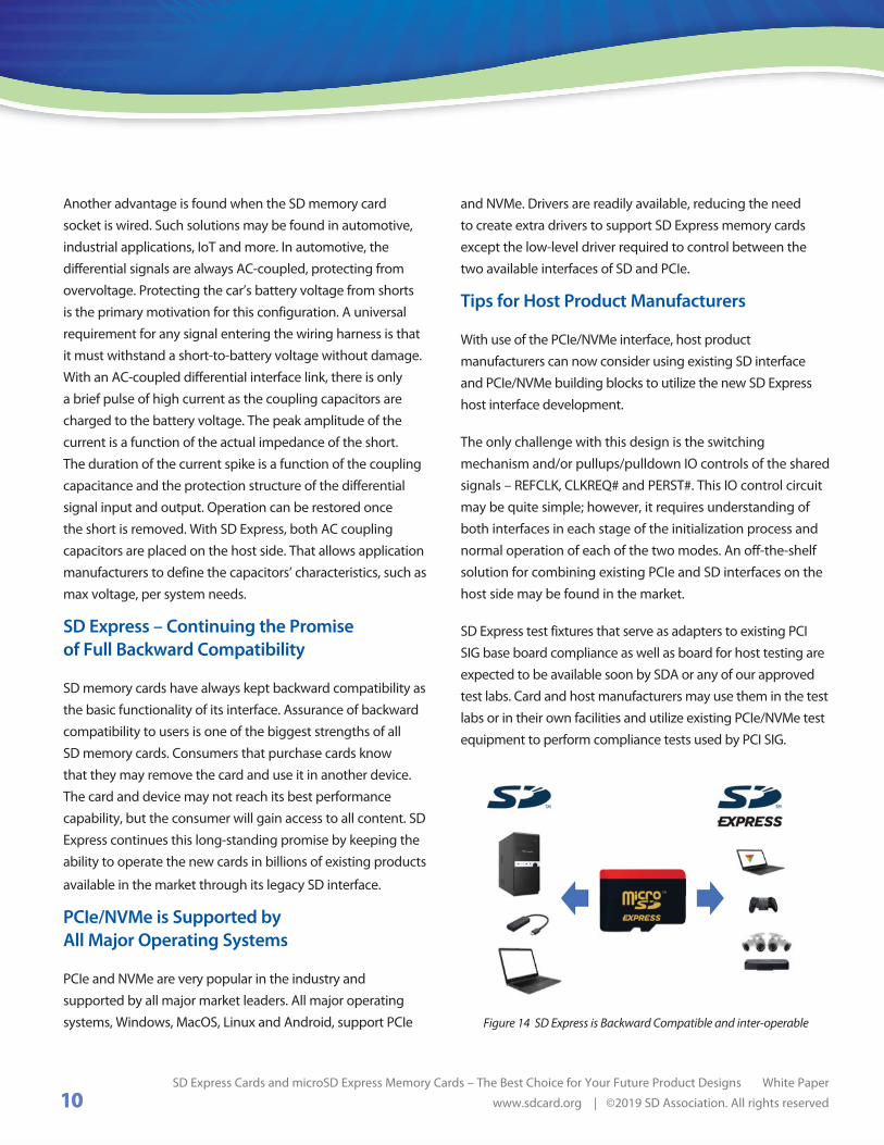
Figure 14 SD Express is Backward Compatible and inter-operable
10

11
Summary
The SD Express specification was introduced to serve new market needs and enable exceptional new experiences for multi-processing environments. This was achieved by providing significant improvement to the reliable, SD and microSD cards which boost them to totally new performance levels. Both SD Express and microSD Express combine the PCIe/NVMe interface with the existing SD interface to deliver impressive results. Choosing SD Express as the choice for all removable card needs means choosing PCIe and NVMe, which are the proven worldwide standards that are the leading specifications for flash memory interfacing. Adoption of SD Express is made even easier thanks to an abundance of existing knowledge and availability of PCIe/NVMe building blocks, from test equipment and drivers to support by all major operating systems.
These new SD memory cards open a whole new world of opportunities and maintain backward compatibility to billions of existing SD host products.
SD Express Cards and microSD Express Memory Cards – The Best Choice for Your Future Product Designs White Paper
www.sdcard.org | ©2019 SD Association. All rights reserved