® Gate Array XC5200 Family A Low-cost Gate Array Alternative.

Scalable Gate Architecture for a One-Dimensional Array of Semiconductor Spin Qubits
D.M. Zajac,1 T. M. Hazard,1 X. Mi,1 E. Nielsen,2 and J. R. Petta11Department of Physics, Princeton University, Princeton, New Jersey 08544, USA
2Sandia National Laboratories, Albuquerque, New Mexico 87185, USA(Received 13 July 2016; revised manuscript received 26 September 2016; published 28 November 2016)
We demonstrate a 12-quantum-dot device fabricated on an undoped Si/SiGe heterostructure as a proofof concept for a scalable, linear gate architecture for semiconductor quantum dots. The device consists ofnine quantum dots in a linear array and three single-quantum-dot charge sensors. We show reproduciblesingle-quantum-dot charging and orbital energies, with standard deviations less than 20% relative tothe mean across the nine-dot array. The single-quantum-dot charge sensors have a charge sensitivity of
8.2 × 10⁻⁴ e=ffiffiffiffiffiffiHz
pand allow for the investigation of real-time charge dynamics. As a demonstration of
the versatility of this device, we use single-shot readout to measure the spin-relaxation time T1 ¼ 170 msat a magnetic field B ¼ 1 T. By reconfiguring the device, we form two capacitively coupled doublequantum dots and extract a mutual charging energy of 200 μeV, which indicates that 50-GHz two-qubitgate-operation speeds are feasible.
DOI: 10.1103/PhysRevApplied.6.054013
I. INTRODUCTION
The density of transistors in integrated circuits has beenfollowing Moore’s law since its conception [1]. However,as the size of transistors approaches the size of a singleatom, the laws of quantum physics will play an increasinglydominant role in computer architectures, making it difficultfor this trend to continue for much longer. Despite this fact,the prospect of utilizing quantum-mechanical phenomenafor information processing offers an opportunity to increasethe power of computers for specific computational prob-lems [2,3]. In order for functional quantum computers tobecome a reality, they will require an on-chip physicalcomponent with reproducible properties that can be incor-porated into large-scale structures, much like the classicalcomputer depends on the robustness of the transistor.One of the leading candidates for the quantum analog of
the transistor is the gate-defined, semiconductor quantum dot[4,5]. The spin state of an electron trapped in a quantum dotis an ideal physical system for storing quantum information[6–8]. Silicon, in particular, with its weak hyperfine fields,small spin-orbit coupling, and lack of piezoelectric electron-phonon coupling, has been shown to support single-spincoherence times as long as 28 ms [9]. However, thefabrication of reliable and scalable Si-based quantum dotshas proved challenging. Independent of the need for a purespin environment, quantum dots must have reproducibleelectrical properties for scaling. The relatively large effectivemass of electrons in Si, along with the typically lowermobilities of Si two-dimensional electron gases, makes thefabrication of tightly confined, few-electron quantum dotswith reproducible properties difficult [10].In this paper, we present a quantum-dot gate architecture
that may allow a path forward for scaling up semiconductor
quantum devices. Our device consists of 12 quantum dots,nine of which are arranged in a linear array and three thatare used as sensitive charge detectors. The enhancement-mode device utilizes an overlapping aluminum gate archi-tecture to achieve tight electronic confinement [11], whilethe undoped Si/SiGe heterostructure provides a clean, high-mobility interface [12] for the formation of well-behavedquantum dots with reproducible characteristics.
II. RESULTS AND DISCUSSION
The outline of the paper is as follows. We first evaluatethe reproducibility of the nine dots in the array byextracting the critical parameters of single quantum dotsformed under each plunger gate: the lever-arm, thecharging energy, and orbital excited-state energy. We areable to reach zero electron occupancy in all nine quantumdots in the array, obtaining an average charging energyEc ¼ 6.9� 0.7 meV and an average orbital energyEorb ¼ 3.0� 0.5 meV. Using adjacent single quantum dotsas charge sensors, we show that we are able to read out thecharge state of the entire array with a signal-to-noise ratio(SNR) that allows for the observation of real-time tunnelingevents. Lastly, as a demonstration of the flexibility of thegate architecture, we perform single-shot spin readout anddemonstrate strong capacitive coupling of two nearest-neighbor double quantum dots (DQDs).
A. Linear gate architecture
A false-color SEM image of the device is shown inFig. 1(a) and a COMSOL simulation of the electron density nin the plane of the quantum well is shown in Fig. 1(b). Inthe upper half of the device, two sets of aluminum gateelectrodes, with a pitch of 100 nm, are interleaved to form a
PHYSICAL REVIEW APPLIED 6, 054013 (2016)
2331-7019=16=6(5)=054013(8) 054013-1 © 2016 American Physical Society
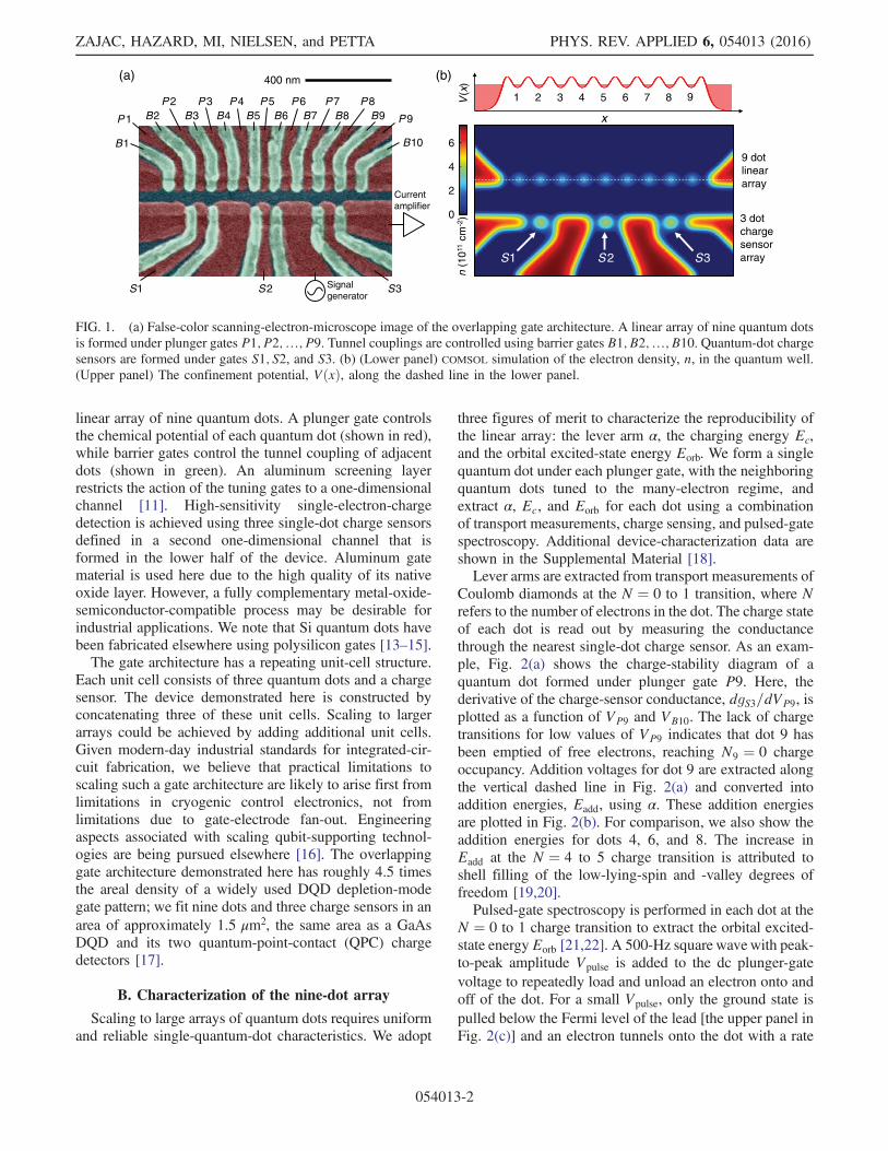
linear array of nine quantum dots. A plunger gate controlsthe chemical potential of each quantum dot (shown in red),while barrier gates control the tunnel coupling of adjacentdots (shown in green). An aluminum screening layerrestricts the action of the tuning gates to a one-dimensionalchannel [11]. High-sensitivity single-electron-chargedetection is achieved using three single-dot charge sensorsdefined in a second one-dimensional channel that isformed in the lower half of the device. Aluminum gatematerial is used here due to the high quality of its nativeoxide layer. However, a fully complementary metal-oxide-semiconductor-compatible process may be desirable forindustrial applications. We note that Si quantum dots havebeen fabricated elsewhere using polysilicon gates [13–15].The gate architecture has a repeating unit-cell structure.
Each unit cell consists of three quantum dots and a chargesensor. The device demonstrated here is constructed byconcatenating three of these unit cells. Scaling to largerarrays could be achieved by adding additional unit cells.Given modern-day industrial standards for integrated-cir-cuit fabrication, we believe that practical limitations toscaling such a gate architecture are likely to arise first fromlimitations in cryogenic control electronics, not fromlimitations due to gate-electrode fan-out. Engineeringaspects associated with scaling qubit-supporting technol-ogies are being pursued elsewhere [16]. The overlappinggate architecture demonstrated here has roughly 4.5 timesthe areal density of a widely used DQD depletion-modegate pattern; we fit nine dots and three charge sensors in anarea of approximately 1.5 μm2, the same area as a GaAsDQD and its two quantum-point-contact (QPC) chargedetectors [17].
B. Characterization of the nine-dot array
Scaling to large arrays of quantum dots requires uniformand reliable single-quantum-dot characteristics. We adopt
three figures of merit to characterize the reproducibility ofthe linear array: the lever arm α, the charging energy Ec,and the orbital excited-state energy Eorb. We form a singlequantum dot under each plunger gate, with the neighboringquantum dots tuned to the many-electron regime, andextract α, Ec, and Eorb for each dot using a combinationof transport measurements, charge sensing, and pulsed-gatespectroscopy. Additional device-characterization data areshown in the Supplemental Material [18].Lever arms are extracted from transport measurements of
Coulomb diamonds at the N ¼ 0 to 1 transition, where Nrefers to the number of electrons in the dot. The charge stateof each dot is read out by measuring the conductancethrough the nearest single-dot charge sensor. As an exam-ple, Fig. 2(a) shows the charge-stability diagram of aquantum dot formed under plunger gate P9. Here, thederivative of the charge-sensor conductance, dgS3=dVP9, isplotted as a function of VP9 and VB10. The lack of chargetransitions for low values of VP9 indicates that dot 9 hasbeen emptied of free electrons, reaching N9 ¼ 0 chargeoccupancy. Addition voltages for dot 9 are extracted alongthe vertical dashed line in Fig. 2(a) and converted intoaddition energies, Eadd, using α. These addition energiesare plotted in Fig. 2(b). For comparison, we also show theaddition energies for dots 4, 6, and 8. The increase inEadd at the N ¼ 4 to 5 charge transition is attributed toshell filling of the low-lying-spin and -valley degrees offreedom [19,20].Pulsed-gate spectroscopy is performed in each dot at the
N ¼ 0 to 1 charge transition to extract the orbital excited-state energy Eorb [21,22]. A 500-Hz square wavewith peak-to-peak amplitude Vpulse is added to the dc plunger-gatevoltage to repeatedly load and unload an electron onto andoff of the dot. For a small Vpulse, only the ground state ispulled below the Fermi level of the lead [the upper panel inFig. 2(c)] and an electron tunnels onto the dot with a rate
(a) (b)400 nm
1 2 3 4 5 6 7 8 9V(x
)
x
S1 S 2 S3
n (1
011
cm-2
)
6
0
2
4
P 7 P 8B8 B9B7
B10
P 9
S1 S2 S3
B2P 2 P 3
B3 B4 B5
B1
P 1 B6P 4 P 5 P 6
9 dot linear array
3 dot charge sensor array
Signal generator
Current amplifier
FIG. 1. (a) False-color scanning-electron-microscope image of the overlapping gate architecture. A linear array of nine quantum dotsis formed under plunger gates P1; P2;…; P9. Tunnel couplings are controlled using barrier gates B1; B2;…; B10. Quantum-dot chargesensors are formed under gates S1; S2, and S3. (b) (Lower panel) COMSOL simulation of the electron density, n, in the quantum well.(Upper panel) The confinement potential, VðxÞ, along the dashed line in the lower panel.
ZAJAC, HAZARD, MI, NIELSEN, and PETTA PHYS. REV. APPLIED 6, 054013 (2016)
054013-2

Γg. When the pulse amplitude exceeds Vorb, the electroncan load into either the ground state or the first excited state[the lower panel in Fig. 2(c)]. The effective loading rate isincreased due to the contribution from the excited state Γeand is visible in the charge-sensing data as a change in theaverage sensor conductance. From these data, we extract anorbital excited-state energy Eorb ¼ αVorb ¼ 3.4 meV fordot 9.Similar characterization is performed on dots 1–8, and
the results are summarized in Table I. The averaged figuresof merit are α¼0.13�0.01meV=mV, Ec¼6.9�0.7meV,
and Eorb ¼ 3.0� 0.5 meV. These charging energies aregenerally larger than those obtained with other devicedesigns in Si/SiGe due to the tight confinement potentialgenerated by the overlapping gate architecture, although stillsmaller than those achieved in Si metal-oxide-semiconductordevices [19]. Specifically, depletion-mode devices haveachieved charging energies of less than 2 meV [23], whileenhancement-mode architectures have yielded chargingenergies close to 5 meV [20]. Moreover, the large orbital-excited-state energies are comparable to those measured inGaAs devices, where the effective mass is nearly 3 timessmaller than the effective mass of electrons in Si [5].
C. Sensitive charge detection
An important criterion for quantum-information process-ing is high-fidelity qubit readout. For both single-shotreadout of an individual spin [24,25] and spin-to-chargeconversion in double- [17] and triple-quantum-dot qubits[26], this criterion translates to a need for high-fidelitycharge-state readout. We demonstrate high-sensitivity chargedetection using the charge-sensor array. The three sensordots give good coverage over the entire nine-dot array.In order to characterize the charge-sensor performance,
we first measure the shift in a charge-sensor Coulomb-blockade peak due to a change in the charge occupancy of anearby dot in the linear array. As an example, in Fig. 3(a),we plot the conductance through charge sensor 3, gS3, as afunction of VP8 and VS3. A Coulomb-blockade peak isvisible in the sensor-dot conductance, and it abruptly shiftseach time an electron is added to quantum dot 8. Wemeasure a peak shift of ΔVS3 ¼ 0.26 mV at the N8 ¼ 0to 1 charge transition. The shift in the charge-sensor-3Coulomb-blockade peak position is also measured for dots2–7 and is plotted in Fig. 3(c) as a function of the geometricdistance, d, between each dot and the sensor dot. The shiftfalls off with a power law that is close to 1=d3.Predictions for the shifts in the sensor-dot Coulomb-
blockade peak position can be obtained by computingthe capacitances of the device. We construct a three-dimensional model of the device based on the wafer growthprofile and lithographic gate dimensions, representing thedots as metallic cylinders with a radius of 19 nm and heightof 5 nm, each centered 7 nm below the Si/SiGe interface.The capacitances of the device are then computed using thefast-multipole-moment solver FastCap [27]. The expectedshift is computed from the simulated capacitances usingΔVS3 ¼ eCm=CpCt, where Cm is the mutual capacitancebetween the sensor dot and the single-electron dot, Cp isthe capacitance between the sensor dot and its plunger gate,and Ct is the total single-electron-dot capacitance [28]. Thecomputed shift scales asΔVS3ðdÞ ∝ 1=d3.02�0.05 and agreesnicely with the experimental data [see the solid black line inFig. 3(c)]. We point out that the accuracy of this model islimited by uncertainty in the exact location of the quantumdots in the quantum well.
-300 VB10 (mV) 100
500
700V
P9
)V
m (
0-10dgS3/dVP9 (arb. units)
N9 = 0
(a)
Electron no. N1 2 3 4 5 6
Ead
d(m
eV)
4.5
7.0 Dot 4Dot 6Dot 8Dot 9
(b)
VP
9(m
V)
585
540400 VPulse (mV)
0-10
Vorb
N9 = 0
N9 = 1
dgS3 /dVP9 (arb. units)(d)(c)
Γe
Γg
Γg
Eorb
Eorb
FIG. 2. (a) Charge-stability diagram of quantum dot 9. Thederivative of charge-sensor-dot-3 conductance, dgS3=dVP9, plot-ted as a function of VP9 and VB10. For low voltages, dot 9 isemptied of free electrons, reaching the N9 ¼ 0 charge state.(b) The addition energy, Eadd, plotted as a function of electronnumber N for dots 4, 6, 8, and 9. (c) Pulsed-gate spectroscopy.The effective tunneling rate onto the dot is dependent on Vpulse.(d) An orbital excited state with energy Eorb ¼ αVorb ¼ 3.4 meVis visible in dot 9.
TABLE I. Lever-arm conversion between the gate voltage andenergy α, charging energy Ec, and orbital excited-state energyEorb for each of the nine dots in the linear array.
Dot α (meV/mV) Ec (meV) Eorb (meV)
1 0.14 6.6 2.72 0.13 6.1 2.63 0.11 5.6 2.14 0.14 7.3 3.35 0.14 7.2 3.36 0.14 7.1 3.07 0.14 7.7 3.58 0.14 7.1 3.49 0.13 7.2 3.4
SCALABLE GATE ARCHITECTURE FOR A ONE- … PHYS. REV. APPLIED 6, 054013 (2016)
054013-3

As in the case of a parallel-plate capacitor, one mightexpect the capacitance to scale as 1=d. However, theoverlapping gate architecture covers nearly the entire Si/SiGe heterostructure with metal, resulting in a significantamount of screening. The impact of this screening can beunderstood using the method of image charges [Fig. 3(d)].An electron trapped in a quantum dot induces a positiveimage charge in the gate metal above. The resulting electricfield due to the electron and its image charge is that of adipole, which falls off with a 1=d3 dependence.
D. Real-time charge detection
The ability to resolve real-time charge dynamics allowsthe study of fundamental physical phenomena at the levelof single electrons [29,30]. It also enables single-shotreadout of single-electron spin states [24,25] and thediscrimination of two-electron singlet and triplet spin states[17]. We now demonstrate high-sensitivity charge detectionthrough the observation of real-time tunneling events[31,32]. Through a quantitative analysis of the charge-sensor response, we extract a charge sensitivity of8.2 × 10−4 e=
ffiffiffiffiffiffiHz
p.
Figure 4(a) shows a color-scale plot of the current Ithrough sensor dot 3 as a function of time, for a range of
plunger-gate voltages VP8, with dot 8 tuned up near theN8 ¼ 0 to 1 charge transition. Five time series extractedfrom this data set are plotted in Fig. 4(b). The lowest timeseries in Fig. 4(b) is acquired with VP8 ¼ 661.12 mV. Herethe dot is empty nearly all of the time. With VP8 slightlyincreased, the current shows signatures of real-time single-electron tunneling events and switches between two levelscorresponding to the N8 ¼ 0 and 1 charge states. Asexpected, the dwell time in the N8 ¼ 1 charge stateincreases with an increasing VP8. Using a threshold todiscriminate between the charge states, we plot the time-averaged occupation of dot 8, hN8i, as a function of VP8 inFig. 4(c). We expect the population to follow a Fermifunction as the chemical potential of the dot level is loweredpast the Fermi level of the lead. The data in Fig. 4(c) arenicely fit to a Fermi function with an electron temper-ature Te ¼ 120 mK.A detailed analysis of the real-time single-electron
tunneling events can be used to determine the charge-sensor SNR and charge sensitivity. We first measure a 1-stime series of the current through the charge sensor with dot8 tuned to the N8 ¼ 0 to 1 charge-degeneracy point. Thedata are acquired at a sampling rate of 500 kHz and aKaiser-Bessel finite-impulse-response (FIR) filter is usedto reduce the effective measurement bandwidth to 30 kHz,the 3-dB point of our room-temperature amplifier. A 30-ms-long segment of this time series is shown in Fig. 5(a).
Image charge
+
-SiGe
Gate metalS1 S2 S3
(a) (b)
(c) (d)
gS3 (e2/h)0.05 0.3
350
400V P
8)
Vm(
213 216
0.05
0.30
213.5 215.5VS3 (mV) VS3 (mV)
g S3
(e2 /
h)
VS3V
S3
)V
m(
0.2
0.0
200 600d (nm)
SiGe
Si
N8 = 0
N8 = 1
N8 = 2
Dot electron
FIG. 3. (a) A Coulomb-blockade peak is visible in sensor-dot-3conductance, gS3, which is plotted as a function of the gatevoltages VP8 and VS3. (b) gS3 measured at the locations indicatedby the dashed lines in (a). The Coulomb-blockade peak shifts byΔVS3 ¼ 0.26 mV when N8 changes by one electron. (c) ΔVS3 ismeasured for dots 2–8 and plotted as a function of the distance dfrom the sensor dot. The black line is the theoretical prediction.(d) The approximately 1=d3 power-law dependence is qualita-tively understood as the field of a dipole formed by the electron inthe quantum well (the blue circle) and its positive image charge(the red circle).
0.5
5.03.5
I (nA)(a)
(c)
(b)
661.0
0 0.5
4
661.0
0
1
0
t (s)
VP 8 (mV) t (s)
I (nA
)
N8
V P8
(mV
) 12
10
6
8
661.8
661.8
N8 = 0
N8 = 1
Dataf (E )
FIG. 4. (a) The current, I, through sensor dot 3, plotted as afunction of VP8 and time, t, near the N8 ¼ 0 to 1 chargetransition. (b) Time series extracted from the data in (a) at thepositions shown by the dashed lines. The dwell time in theN8 ¼ 1 charge state increases as VP8 is made more positive. Thetraces are offset by 2 nA for clarity. (c) Time-averaged quantum-dot-8 occupation, hN8i, extracted from the data in (a) and plottedas a function of VP8. The data are fit to a Fermi function fðEÞ.
ZAJAC, HAZARD, MI, NIELSEN, and PETTA PHYS. REV. APPLIED 6, 054013 (2016)
054013-4
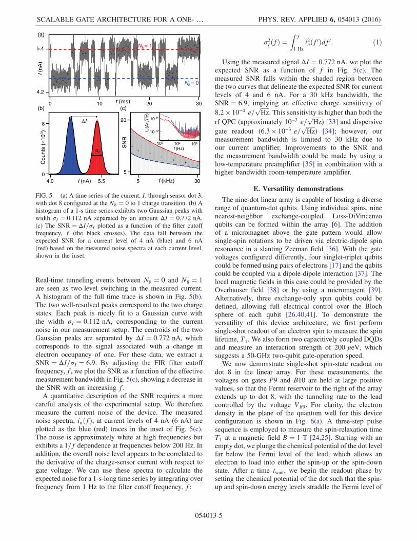
Real-time tunneling events between N8 ¼ 0 and N8 ¼ 1are seen as two-level switching in the measured current.A histogram of the full time trace is shown in Fig. 5(b).The two well-resolved peaks correspond to the two chargestates. Each peak is nicely fit to a Gaussian curve withthe width σI ¼ 0.112 nA, corresponding to the currentnoise in our measurement setup. The centroids of the twoGaussian peaks are separated by ΔI ¼ 0.772 nA, whichcorresponds to the signal associated with a change inelectron occupancy of one. For these data, we extract aSNR ¼ ΔI=σI ¼ 6.9. By adjusting the FIR filter cutofffrequency, f, we plot the SNR as a function of the effectivemeasurement bandwidth in Fig. 5(c), showing a decrease inthe SNR with an increasing f.A quantitative description of the SNR requires a more
careful analysis of the experimental setup. We thereforemeasure the current noise of the device. The measurednoise spectra, inðfÞ, at current levels of 4 nA (6 nA) areplotted as the blue (red) traces in the inset of Fig. 5(c).The noise is approximately white at high frequencies butexhibits a 1=f dependence at frequencies below 200 Hz. Inaddition, the overall noise level appears to be correlated tothe derivative of the charge-sensor current with respect togate voltage. We can use these spectra to calculate theexpected noise for a 1-s-long time series by integrating overfrequency from 1 Hz to the filter cutoff frequency, f:
σ2I ðfÞ ¼Z
f
1 Hzi2nðf0Þdf0: ð1Þ
Using the measured signal ΔI ¼ 0.772 nA, we plot theexpected SNR as a function of f in Fig. 5(c). Themeasured SNR falls within the shaded region betweenthe two curves that delineate the expected SNR for currentlevels of 4 and 6 nA. For a 30 kHz bandwidth, theSNR ¼ 6.9, implying an effective charge sensitivity of8.2 × 10−4 e=
ffiffiffiffiffiffiHz
p. This sensitivity is higher than both the
rf QPC (approximately 10−3 e=ffiffiffiffiffiffiHz
p) [33] and dispersive
gate readout (6.3 × 10⁻³ e=ffiffiffiffiffiffiHz
p) [34]; however, our
measurement bandwidth is limited to 30 kHz due toour current amplifier. Improvements to the SNR andthe measurement bandwidth could be made by using alow-temperature preamplifier [35] in combination with ahigher bandwidth room-temperature amplifier.
E. Versatility demonstrations
The nine-dot linear array is capable of hosting a diverserange of quantum-dot qubits. Using individual spins, ninenearest-neighbor exchange-coupled Loss-DiVincenzoqubits can be formed within the array [6]. The additionof a micromagnet above the gate pattern would allowsingle-spin rotations to be driven via electric-dipole spinresonance in a slanting Zeeman field [36]. With the gatevoltages configured differently, four singlet-triplet qubitscould be formed using pairs of electrons [17] and the qubitscould be coupled via a dipole-dipole interaction [37]. Thelocal magnetic fields in this case could be provided by theOverhauser field [38] or by using a micromagent [39].Alternatively, three exchange-only spin qubits could bedefined, allowing full electrical control over the Blochsphere of each qubit [26,40,41]. To demonstrate theversatility of this device architecture, we first performsingle-shot readout of an electron spin to measure the spinlifetime, T1. We also form two capacitively coupled DQDsand measure an interaction strength of 200 μeV, whichsuggests a 50-GHz two-qubit gate-operation speed.We now demonstrate single-shot spin-state readout on
dot 8 in the linear array. For these measurements, thevoltages on gates P9 and B10 are held at large positivevalues, so that the Fermi reservoir to the right of the arrayextends up to dot 8, with the tunneling rate to the leadcontrolled by the voltage VB9. For clarity, the electrondensity in the plane of the quantum well for this deviceconfiguration is shown in Fig. 6(a). A three-step pulsesequence is employed to measure the spin-relaxation timeT1 at a magnetic field B ¼ 1 T [24,25]. Starting with anempty dot, we plunge the chemical potential of the dot levelfar below the Fermi level of the lead, which allows anelectron to load into either the spin-up or the spin-downstate. After a time twait, we begin the readout phase bysetting the chemical potential of the dot such that the spin-up and spin-down energy levels straddle the Fermi level of
(a)
(b) (c)
I (nA
)C
ount
s (×
103)
I (nA) f (kHz)
SN
R
3020100 t (ms)
5.54.0
5
5.4
4.2
8
0
20
5 30
N8 = 0
N8 = 1
100 102 104
10-12
10-11
i n(A
/)
f (Hz)
FIG. 5. (a) A time series of the current, I, through sensor dot 3,with dot 8 configured at the N8 ¼ 0 to 1 charge transition. (b) Ahistogram of a 1-s time series exhibits two Gaussian peaks withwidth σI ¼ 0.112 nA separated by an amount ΔI ¼ 0.772 nA.(c) The SNR ¼ ΔI=σI plotted as a function of the filter cutofffrequency, f (the black crosses). The data fall between theexpected SNR for a current level of 4 nA (blue) and 6 nA(red) based on the measured noise spectra at each current level,shown in the inset.
SCALABLE GATE ARCHITECTURE FOR A ONE- … PHYS. REV. APPLIED 6, 054013 (2016)
054013-5
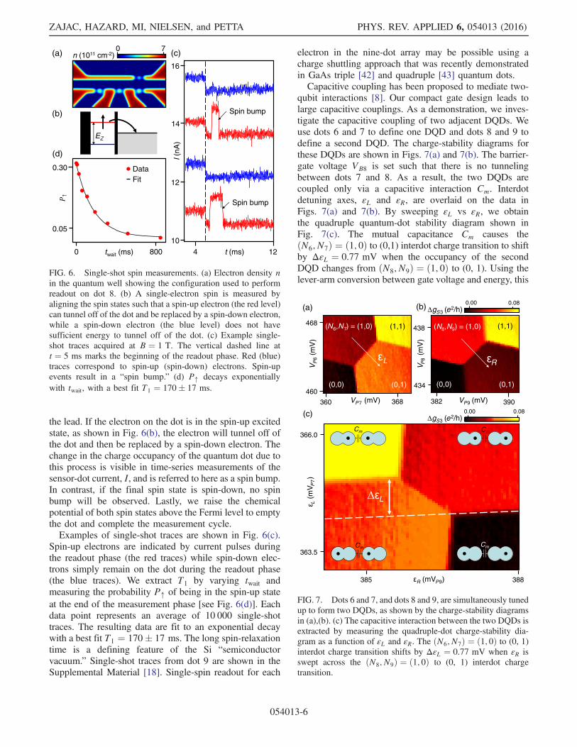
the lead. If the electron on the dot is in the spin-up excitedstate, as shown in Fig. 6(b), the electron will tunnel off ofthe dot and then be replaced by a spin-down electron. Thechange in the charge occupancy of the quantum dot due tothis process is visible in time-series measurements of thesensor-dot current, I, and is referred to here as a spin bump.In contrast, if the final spin state is spin-down, no spinbump will be observed. Lastly, we raise the chemicalpotential of both spin states above the Fermi level to emptythe dot and complete the measurement cycle.Examples of single-shot traces are shown in Fig. 6(c).
Spin-up electrons are indicated by current pulses duringthe readout phase (the red traces) while spin-down elec-trons simply remain on the dot during the readout phase(the blue traces). We extract T1 by varying twait andmeasuring the probability P↑ of being in the spin-up stateat the end of the measurement phase [see Fig. 6(d)]. Eachdata point represents an average of 10 000 single-shottraces. The resulting data are fit to an exponential decaywith a best fit T1 ¼ 170� 17 ms. The long spin-relaxationtime is a defining feature of the Si “semiconductorvacuum.” Single-shot traces from dot 9 are shown in theSupplemental Material [18]. Single-spin readout for each
electron in the nine-dot array may be possible using acharge shuttling approach that was recently demonstratedin GaAs triple [42] and quadruple [43] quantum dots.Capacitive coupling has been proposed to mediate two-
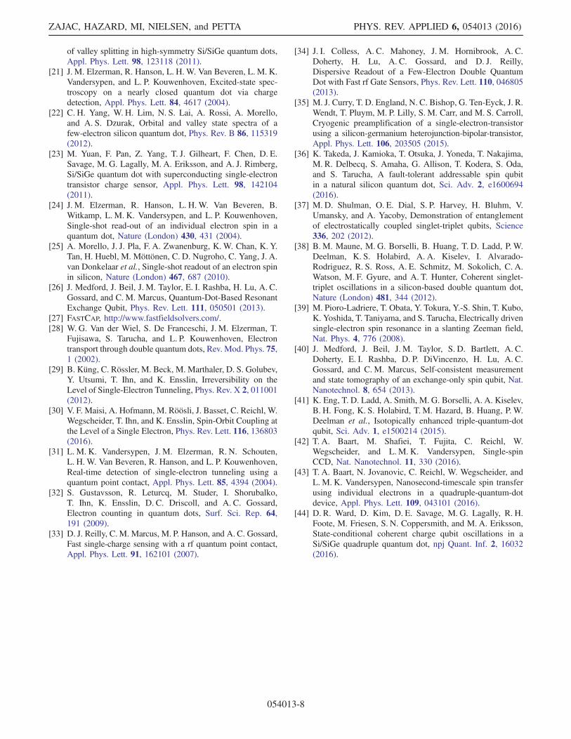
qubit interactions [8]. Our compact gate design leads tolarge capacitive couplings. As a demonstration, we inves-tigate the capacitive coupling of two adjacent DQDs. Weuse dots 6 and 7 to define one DQD and dots 8 and 9 todefine a second DQD. The charge-stability diagrams forthese DQDs are shown in Figs. 7(a) and 7(b). The barrier-gate voltage VB8 is set such that there is no tunnelingbetween dots 7 and 8. As a result, the two DQDs arecoupled only via a capacitive interaction Cm. Interdotdetuning axes, εL and εR, are overlaid on the data inFigs. 7(a) and 7(b). By sweeping εL vs εR, we obtainthe quadruple quantum-dot stability diagram shown inFig. 7(c). The mutual capacitance Cm causes theðN6; N7Þ ¼ ð1; 0Þ to (0,1) interdot charge transition to shiftby ΔεL ¼ 0.77 mV when the occupancy of the secondDQD changes from ðN8; N9Þ ¼ ð1; 0Þ to (0, 1). Using thelever-arm conversion between gate voltage and energy, this
12
(a)
(d)
(c)
10
0
0.05
0.30
4twait (ms) t (ms)
I (nA
)
16
14
12
800
DataFit
EZ
Spin bump
Spin bump
(b)
0 7n (1011 cm-2)
FIG. 6. Single-shot spin measurements. (a) Electron density nin the quantum well showing the configuration used to performreadout on dot 8. (b) A single-electron spin is measured byaligning the spin states such that a spin-up electron (the red level)can tunnel off of the dot and be replaced by a spin-down electron,while a spin-down electron (the blue level) does not havesufficient energy to tunnel off of the dot. (c) Example single-shot traces acquired at B ¼ 1 T. The vertical dashed line att ¼ 5 ms marks the beginning of the readout phase. Red (blue)traces correspond to spin-up (spin-down) electrons. Spin-upevents result in a “spin bump.” (d) P↑ decays exponentiallywith twait, with a best fit T1 ¼ 170� 17 ms.
(a)
(c)
(b)
468
460
360 368
438
434
382 390
363.5
366.0
VP7 (mV) VP9 (mV)
L(m
V P7)
V P8
(mV
)
VP
6(m
V)
gS3 (e2/h)0.00 0.08
R (mVP9)385 388
L R
L
(0,0)
(N6,N7) = (1,0)
(0,1) (0,0) (0,1)
gS3 (e2/h)0.080.00
(1,1) (1,1)
Cm
Cm
Cm
Cm
(N8,N9) = (1,0)
FIG. 7. Dots 6 and 7, and dots 8 and 9, are simultaneously tunedup to form two DQDs, as shown by the charge-stability diagramsin (a),(b). (c) The capacitive interaction between the two DQDs isextracted by measuring the quadruple-dot charge-stability dia-gram as a function of εL and εR. The ðN6; N7Þ ¼ ð1; 0Þ to (0, 1)interdot charge transition shifts by ΔεL ¼ 0.77 mV when εR isswept across the ðN8; N9Þ ¼ ð1; 0Þ to (0, 1) interdot chargetransition.
ZAJAC, HAZARD, MI, NIELSEN, and PETTA PHYS. REV. APPLIED 6, 054013 (2016)
054013-6

change corresponds to a 200-μeV energy shift (50-GHztwo-qubit gate-operation time) [44]. By reducing thevoltage VB8 on the barrier gate that separates the DQDsby 60 mV, we are able to reduce the coupling energy scalefrom 200 to 100 μeV. The coupling could be furtherreduced by increasing the lithographic distance betweenthe two dots. As a further demonstration of devicetunability, we show in the Supplemental Material that afew-electron triple quantum dot can be formed using dots7–9 [18].
III. CONCLUSION
In summary, we develop a scalable one-dimensionalquantum-dot gate architecture that yields quantum dotswith uniform and reproducible characteristics. As a proof ofconcept, we have presented a 12-quantum-dot deviceconsisting of a linear array of nine quantum dots and threesingle-quantum-dot charge sensors. From characterizationmeasurements, we obtain standard deviations in the charg-ing energies and orbital energies of less than 20% relative totheir means: Ec ¼ 6.9� 0.7 meV, Eorb ¼ 3.0� 0.5 meV.We demonstrate the ability to detect real-time tunnelingevents in this large array, and we use this capability forsingle-shot measurements of the electron spin. As a finaldemonstration, we characterize the dipole-dipole couplingof two adjacent DQDs formed in the array and measure aninteraction energy of 200 μeV, which bodes well forcomputing architectures that rely on capacitive couplingof the qubits.
ACKNOWLEDGMENTS
This work is funded by the ARO through GrantNo. W911NF-15-1-0149, the Gordon and Betty MooreFoundation’s EPiQS Initiative through GrantNo. GBMF4535, and the NSF (Grants No. DMR-1409556and No. DMR-1420541). Devices were fabricated in thePrinceton University Quantum Device NanofabricationLaboratory.
[1] G. E. Moore, Cramming more components onto integratedcircuits, Electronics 38, 8 (1965).
[2] P. W. Shor, Polynomial-time algorithms for prime factori-zation and discrete logarithms on a quantum computer,SIAM Rev. 41, 303 (1999).
[3] L. K. Grover, in Proceedings of the 28th Annual ACMSymposium on Theory of Computing, Philadelphia, PA,USA, 1996 (ACM, New York, 1996), p. 212.
[4] L. P. Kouwenhoven, C.M.Marcus, P. L.McEuen, S. Tarucha,R.M. Westervelt, and N. S. Wingreen, Mesoscopic ElectronTransport (Springer, New York, 1997).
[5] R. Hanson, L. P. Kouwenhoven, J. R. Petta, S. Tarucha, andL. M. K. Vandersypen, Spins in few-electron quantum dots,Rev. Mod. Phys. 79, 1217 (2007).
[6] D. Loss and D. P. DiVincenzo, Quantum computation withquantum dots, Phys. Rev. A 57, 120 (1998).
[7] D. P. DiVincenzo, D. Bacon, J. Kempe, G. Burkard, andK. B. Whaley, Universal quantum computation with theexchange interaction, Nature (London) 408, 339 (2000).
[8] J. M. Taylor, H.-A. Engel, W. Dür, A. Yacoby, C. M.Marcus, P. Zoller, and M. D. Lukin, Fault-tolerant archi-tecture for quantum computation using electrically con-trolled semiconductor spins, Nat. Phys. 1, 177 (2005).
[9] M. Veldhorst, J. C. C. Hwang, C. H. Yang, A.W. Leenstra,B. De Ronde, J. P. Dehollain, J. T. Muhonen, F. E. Hudson,K. M. Itoh, A. Morello et al., An addressable quantum dotqubit with fault-tolerant control-fidelity, Nat. Nanotechnol.9, 981 (2014).
[10] C. Payette, K. Wang, P. J. Koppinen, Y. Dovzhenko, J. C.Sturm, and J. R. Petta, Single charge sensing and transportin double quantum dots fabricated from commerciallygrown Si/SiGe heterostructures, Appl. Phys. Lett. 100,043508 (2012).
[11] D. M. Zajac, T. M. Hazard, X. Mi, K. Wang, and J. R. Petta,A reconfigurable gate architecture for Si/SiGe quantumdots, Appl. Phys. Lett. 106, 223507 (2015).
[12] X. Mi, T. M. Hazard, C. Payette, K. Wang, D. M. Zajac, J. V.Cady, and J. R. Petta, Magnetotransport studies of mobilitylimiting mechanisms in undoped Si/SiGe heterostructures,Phys. Rev. B 92, 035304 (2015).
[13] M. F. Gonzalez-Zalba, S. N. Shevchenko, S. Barraud, J. R.Johansson, A. J. Ferguson, F. Nori, and A. C. Betz, Gate-sensing coherent charge oscillations in a silicon field-effecttransistor, Nano Lett. 16, 1614 (2016).
[14] T. M. Lu, N. C. Bishop, T. Pluym, J. Means, P. G. Kotula, J.Cederberg, L. A. Tracy, J. Dominguez, M. P. Lilly, and M. S.Carroll, Enhancement-mode buried strained silicon channelquantum dot with tunable lateral geometry, Appl. Phys. Lett.99, 043101 (2011).
[15] L. A. Tracy, E. P. Nordberg, R. W. Young, C. B. Pinilla, H.L. Stalford, G. A. Ten Eyck, K. Eng, K. D. Childs, J. R.Wendt, R. K. Grubbs et al., Double quantum dot withtunable coupling in an enhancement-mode silicon metal-oxide semiconductor device with lateral geometry, Appl.Phys. Lett. 97, 192110 (2010).
[16] J. Hornibrook, J. Colless, I. C. Lamb, S. Pauka, H. Lu, A.Gossard, J. Watson, G. Gardner, S. Fallahi, M. Manfra et al.,Cryogenic Control Architecture for Large-Scale QuantumComputing, Phys. Rev. Applied 3, 024010 (2015).
[17] J. R. Petta, A. C. Johnson, J. M. Taylor, E. A. Laird, A.Yacoby, M. D. Lukin, C. M. Marcus, M. P. Hanson, andA. C. Gossard, Coherent manipulation of coupled electronspins in semiconductor quantum dots, Science 309, 2180(2005).
[18] See Supplemental Material at http://link.aps.org/supplemental/10.1103/PhysRevApplied.6.054013 for addi-tional device-characterization data.
[19] C. H.Yang, A. Rossi, R. Ruskov, N. S. Lai, F. A.Mohiyaddin,S. Lee, C. Tahan, G. Klimeck, A. Morello, and A. S. Dzurak,Spin-valley lifetimes in a silicon quantum dot with tunablevalley splitting, Nat. Commun. 4, 2069 (2013).
[20] M. G. Borselli, R. S. Ross, A. A. Kiselev, E. T. Croke, K. S.Holabird, P. W. Deelman, L. D. Warren, I. Alvarado-Rodriguez, I. Milosavljevic, F. C. Ku et al., Measurement
SCALABLE GATE ARCHITECTURE FOR A ONE- … PHYS. REV. APPLIED 6, 054013 (2016)
054013-7
of valley splitting in high-symmetry Si/SiGe quantum dots,Appl. Phys. Lett. 98, 123118 (2011).
[21] J. M. Elzerman, R. Hanson, L. H. W. Van Beveren, L. M. K.Vandersypen, and L. P. Kouwenhoven, Excited-state spec-troscopy on a nearly closed quantum dot via chargedetection, Appl. Phys. Lett. 84, 4617 (2004).
[22] C. H. Yang, W. H. Lim, N. S. Lai, A. Rossi, A. Morello,and A. S. Dzurak, Orbital and valley state spectra of afew-electron silicon quantum dot, Phys. Rev. B 86, 115319(2012).
[23] M. Yuan, F. Pan, Z. Yang, T. J. Gilheart, F. Chen, D. E.Savage, M. G. Lagally, M. A. Eriksson, and A. J. Rimberg,Si/SiGe quantum dot with superconducting single-electrontransistor charge sensor, Appl. Phys. Lett. 98, 142104(2011).
[24] J. M. Elzerman, R. Hanson, L. H. W. Van Beveren, B.Witkamp, L. M. K. Vandersypen, and L. P. Kouwenhoven,Single-shot read-out of an individual electron spin in aquantum dot, Nature (London) 430, 431 (2004).
[25] A. Morello, J. J. Pla, F. A. Zwanenburg, K. W. Chan, K. Y.Tan, H. Huebl, M. Möttönen, C. D. Nugroho, C. Yang, J. A.van Donkelaar et al., Single-shot readout of an electron spinin silicon, Nature (London) 467, 687 (2010).
[26] J. Medford, J. Beil, J. M. Taylor, E. I. Rashba, H. Lu, A. C.Gossard, and C. M. Marcus, Quantum-Dot-Based ResonantExchange Qubit, Phys. Rev. Lett. 111, 050501 (2013).
[27] FASTCAP, http://www.fastfieldsolvers.com/.[28] W. G. Van der Wiel, S. De Franceschi, J. M. Elzerman, T.
Fujisawa, S. Tarucha, and L. P. Kouwenhoven, Electrontransport through double quantum dots, Rev. Mod. Phys. 75,1 (2002).
[29] B. Küng, C. Rössler, M. Beck, M. Marthaler, D. S. Golubev,Y. Utsumi, T. Ihn, and K. Ensslin, Irreversibility on theLevel of Single-Electron Tunneling, Phys. Rev. X 2, 011001(2012).
[30] V. F. Maisi, A. Hofmann, M. Röösli, J. Basset, C. Reichl, W.Wegscheider, T. Ihn, and K. Ensslin, Spin-Orbit Coupling atthe Level of a Single Electron, Phys. Rev. Lett. 116, 136803(2016).
[31] L. M. K. Vandersypen, J. M. Elzerman, R. N. Schouten,L. H. W. Van Beveren, R. Hanson, and L. P. Kouwenhoven,Real-time detection of single-electron tunneling using aquantum point contact, Appl. Phys. Lett. 85, 4394 (2004).
[32] S. Gustavsson, R. Leturcq, M. Studer, I. Shorubalko,T. Ihn, K. Ensslin, D. C. Driscoll, and A. C. Gossard,Electron counting in quantum dots, Surf. Sci. Rep. 64,191 (2009).
[33] D. J. Reilly, C.M. Marcus, M. P. Hanson, and A. C. Gossard,Fast single-charge sensing with a rf quantum point contact,Appl. Phys. Lett. 91, 162101 (2007).
[34] J. I. Colless, A. C. Mahoney, J. M. Hornibrook, A. C.Doherty, H. Lu, A. C. Gossard, and D. J. Reilly,Dispersive Readout of a Few-Electron Double QuantumDot with Fast rf Gate Sensors, Phys. Rev. Lett. 110, 046805(2013).
[35] M. J. Curry, T. D. England, N. C. Bishop, G. Ten-Eyck, J. R.Wendt, T. Pluym, M. P. Lilly, S. M. Carr, and M. S. Carroll,Cryogenic preamplification of a single-electron-transistorusing a silicon-germanium heterojunction-bipolar-transistor,Appl. Phys. Lett. 106, 203505 (2015).
[36] K. Takeda, J. Kamioka, T. Otsuka, J. Yoneda, T. Nakajima,M. R. Delbecq, S. Amaha, G. Allison, T. Kodera, S. Oda,and S. Tarucha, A fault-tolerant addressable spin qubitin a natural silicon quantum dot, Sci. Adv. 2, e1600694(2016).
[37] M. D. Shulman, O. E. Dial, S. P. Harvey, H. Bluhm, V.Umansky, and A. Yacoby, Demonstration of entanglementof electrostatically coupled singlet-triplet qubits, Science336, 202 (2012).
[38] B. M. Maune, M. G. Borselli, B. Huang, T. D. Ladd, P. W.Deelman, K. S. Holabird, A. A. Kiselev, I. Alvarado-Rodriguez, R. S. Ross, A. E. Schmitz, M. Sokolich, C. A.Watson, M. F. Gyure, and A. T. Hunter, Coherent singlet-triplet oscillations in a silicon-based double quantum dot,Nature (London) 481, 344 (2012).
[39] M. Pioro-Ladriere, T. Obata, Y. Tokura, Y.-S. Shin, T. Kubo,K. Yoshida, T. Taniyama, and S. Tarucha, Electrically drivensingle-electron spin resonance in a slanting Zeeman field,Nat. Phys. 4, 776 (2008).
[40] J. Medford, J. Beil, J. M. Taylor, S. D. Bartlett, A. C.Doherty, E. I. Rashba, D. P. DiVincenzo, H. Lu, A. C.Gossard, and C. M. Marcus, Self-consistent measurementand state tomography of an exchange-only spin qubit, Nat.Nanotechnol. 8, 654 (2013).
[41] K. Eng, T. D. Ladd, A. Smith, M. G. Borselli, A. A. Kiselev,B. H. Fong, K. S. Holabird, T. M. Hazard, B. Huang, P. W.Deelman et al., Isotopically enhanced triple-quantum-dotqubit, Sci. Adv. 1, e1500214 (2015).
[42] T. A. Baart, M. Shafiei, T. Fujita, C. Reichl, W.Wegscheider, and L. M. K. Vandersypen, Single-spinCCD, Nat. Nanotechnol. 11, 330 (2016).
[43] T. A. Baart, N. Jovanovic, C. Reichl, W. Wegscheider, andL. M. K. Vandersypen, Nanosecond-timescale spin transferusing individual electrons in a quadruple-quantum-dotdevice, Appl. Phys. Lett. 109, 043101 (2016).
[44] D. R. Ward, D. Kim, D. E. Savage, M. G. Lagally, R. H.Foote, M. Friesen, S. N. Coppersmith, and M. A. Eriksson,State-conditional coherent charge qubit oscillations in aSi/SiGe quadruple quantum dot, npj Quant. Inf. 2, 16032(2016).
ZAJAC, HAZARD, MI, NIELSEN, and PETTA PHYS. REV. APPLIED 6, 054013 (2016)
054013-8