SC6006: Operation Manual - power electronics drives... · The SC6006 is also a...
59
SC6006: Operation Manual 130320 Rev.:2.3 3 8 9 10 11 12 13 14 15 16 17 18 19 20 21 4 5 6 7 22 N R S T PWR RESET EXT BLK OV CURR FAULT FIRING SC6006 G6 K6 K5 G5 K4 G4 K3 G3 K2 G2 K1 G1 MENU OK ALPHA U_SENS I_SENS U_SET I_SET I_SENS U_SENS LCD CONTRAST COARSE FINE 1 2 SEMICODE ELECTRONICA ® SC6006
Transcript of SC6006: Operation Manual - power electronics drives... · The SC6006 is also a...
SC6006: Operation Manual
130
320
Re
v.:2
.3
3 8 9 10 11 12 13 14 15 16 17 18 19 20 214 5 6 7 22
N RST
PWR
RESET
EXT BLKOV CURR
FAULTFIRING
SC6006
G6 K6K5G5K4G4K3G3K2G2K1G1
MENU OK
ALPHAU_SENSI_SENSU_SETI_SETI_SENSU_SENS
LCD
CO
NT
RA
ST
COARSE FINE
1 2
SE
MIC
OD
EE
LEC
TR
ON
ICA
®
SC
600
6
Index of contents 1 GENERAL.................................................................................................................................................... 4
1.1 Special Features................................................................................................................................... 4 1.2 Warranty............................................................................................................................................... 4
2 SAFETY INSTRUCTIONS............................................................................................................................ 5 2.1 Operator and personnel requirements..................................................................................................5 2.2 Proper and intended use......................................................................................................................5 2.3 Use and operation of the device...........................................................................................................5
3 FUNCTIONS................................................................................................................................................. 6 3.1 Topology configuration..........................................................................................................................6 3.2 Operating modes.................................................................................................................................. 6 3.3 Setpoint signals processing.................................................................................................................. 9
3.3.1 Analog or digital references / setpoints.........................................................................................9 3.3.2 Setpoints signal processing diagrams..........................................................................................9
3.4 Feedback signals processing..............................................................................................................11 3.5 Setpoints and feedback live input signals configuration.....................................................................12 3.6 Control Modes.................................................................................................................................... 12 3.7 Soft power ON and soft power OFF...................................................................................................13 3.8 Fault sources and pulse inhibition......................................................................................................14 3.9 Start up mode..................................................................................................................................... 15 3.10 Autoset function................................................................................................................................ 15 3.11 Output assignation option................................................................................................................. 16 3.12 Saving all the changes and configurations.......................................................................................16 3.13 Restore default configurations..........................................................................................................16
4 SETTINGS AND OPERATION................................................................................................................... 17 4.1 PCB connectors overview................................................................................................................... 17 4.2 Connectors......................................................................................................................................... 18
4.2.1 Power supply connector (J1)......................................................................................................18 4.2.2 Synchronism connector (J11).....................................................................................................18 4.2.3 Feedback voltage signal connector (J12)...................................................................................19 4.2.4 External block and dry output fault connector (J13)....................................................................19 4.2.5 Current input feedback connector (J14).....................................................................................20 4.2.6 Setpoints and inhibit connector (J15).........................................................................................21 4.2.7 Feedback and alpha setpoint input connector (J16)...................................................................22 4.2.8 Output SCR firing connectors (SCR1-SCR6).............................................................................23 4.2.9 Serial communications DB-9 connector (J32).............................................................................23
4.3 LCD menu settings and navigation.....................................................................................................24 4.3.1 Main Menu:................................................................................................................................. 24
4.3.1.1 LCD contrast adjusting potentiometer................................................................................25 4.3.1.2 LCD backlight..................................................................................................................... 25
4.3.2 Settings menu............................................................................................................................. 25 4.3.2.1 Topology option.................................................................................................................. 25 4.3.2.2 Mode option........................................................................................................................ 26 4.3.2.3 Reference submenu...........................................................................................................26 4.3.2.4 Live-zero input submenu....................................................................................................26 4.3.2.5 Control option..................................................................................................................... 26 4.3.2.6 Soft ON/OFF ramps submenu............................................................................................26 4.3.2.7 Faults submenu.................................................................................................................. 27 4.3.2.8 Start up option.................................................................................................................... 27 4.3.2.9 Autoset options submenu...................................................................................................28 4.3.2.10 Outputs assignation submenu..........................................................................................28 4.3.2.11 Communications submenu...............................................................................................28 4.3.2.12 Save changes option........................................................................................................28 4.3.2.13 Restore option.................................................................................................................. 29
4.3.3 Registers menu.......................................................................................................................... 29 4.3.4 Debug menu............................................................................................................................... 30
4.4 Jumpers and DIP Switches configurations.........................................................................................30
2
4.4.1 Jumpers J7 and J20 to J24........................................................................................................30 4.4.2 DIP Switches.............................................................................................................................. 31 4.4.3 Setting the gain for direct voltage feedback input.......................................................................32
4.5 LED Indications.................................................................................................................................. 32 5 SERIAL COMMUNICATION....................................................................................................................... 33
5.1 Overview available command set.......................................................................................................34 5.2 Query instruction set........................................................................................................................... 34
5.2.1 “?ver” query version command...................................................................................................34 5.2.2 “?S” query status register...........................................................................................................34 5.2.3 “?A” query alpha register............................................................................................................34 5.2.4 “?U” query voltage register.........................................................................................................34 5.2.5 “?I” query current register...........................................................................................................34
5.3 Signal instruction set.......................................................................................................................... 34 5.3.1 “*OK” signal command...............................................................................................................35 5.3.2 “*MENU” signal command..........................................................................................................35 5.3.3 “*UP” signal command................................................................................................................35 5.3.4 “*DW” signal command...............................................................................................................35 5.3.5 “*RMT” signal command.............................................................................................................35 5.3.6 “*ECHO” signal command..........................................................................................................35 5.3.7 “*HOME” signal command..........................................................................................................35 5.3.8 “*RST” signal command.............................................................................................................35 5.3.9 “*SV” signal command................................................................................................................35
5.4 Memory read instruction..................................................................................................................... 36 5.5 Memory write instruction..................................................................................................................... 36
6 INTERNAL MEMORY AND REGISTERS...................................................................................................37 6.1 Readable registers............................................................................................................................. 37
6.1.1 status registers........................................................................................................................... 37 6.1.2 p_status registers....................................................................................................................... 38
6.2 Writable registers................................................................................................................................ 40 7 INSTALLATION........................................................................................................................................... 41
7.1 Typical application circuits.................................................................................................................. 41 7.2 Control AC/AC applications................................................................................................................41
7.2.1 W3C topology connection example............................................................................................41 7.2.2 W3C current and voltage feedback scheme...............................................................................42 7.2.3 Load connection types for W3C scheme....................................................................................42 7.2.4 M6CK and M3.2CK schemes of connection...............................................................................43
7.3 Control AC/DC applications. B6C scheme..........................................................................................44 7.3.1 B6C topology connection example.............................................................................................44 7.3.2 DC current sense feedback using a shunt..................................................................................44 7.3.3 Feedback using a current and voltage isolated sensors.............................................................45
7.4 Direct drive mode with block signal....................................................................................................46 7.5 Mounting recommendations...............................................................................................................48
7.5.1 General mounting recommendations..........................................................................................48 7.5.2 Recommended start up procedure.............................................................................................48 7.5.3 Notes about the control card in systems controlled by microcontrollers or PLC.........................49
8 AVAILABLE ACCESSORIES...................................................................................................................... 50 8.1 SCRP6006.......................................................................................................................................... 50
8.1.1 Interfacing SC6006 with remote panel SCRP6006.....................................................................50 8.2 SCGI24............................................................................................................................................... 51
8.2.1 Galvanically isolated current loop with shunt using SCGI24.......................................................51 8.3 SCST700............................................................................................................................................ 52
8.3.1 Obtaining a neutral reference using SCST700 for improved synchronism aquisition.................52 9 FIRMWARE REVISIONS............................................................................................................................ 53 10 TECHNICAL SPECIFICATIONS...............................................................................................................54
10.1 Mechanical dimensions.................................................................................................................... 58 10.2 Connectors overview........................................................................................................................ 58
3

1 GENERAL
These operation instructions describe the configuration and functions of the SC6006 and are designed toenable qualified personnel to perform the planning, commissioning and maintenance of this equipment.
These operation instructions comply with the current technical specifications of the device at the time ofpublication. The contents do not constitute a subject matter of the contract, but serve for informationpurposes only.
We reserve the right to alter any specification given in these operating instructions, especially with regard totechnical data and operation. SEMICODE reserves the right to make modifications with regard to the contentand technical data in these operation instructions.
Versatility and ruggedness are the main features of SC6006 providing a lot of regulation options and a greatperformance in many different applications and environments.
SC6006 is designed to adapt to most common rectification and control schemes, like W3C, B6C, M6C andM3.2C. Optionally can also be applied to W3H, B6H and M3C. The power adjustment can be made bycurrent or voltage through potentiometers or by external analog signals. SC6006 also has protection againstcurrent peaks, soft start up ramp, inhibit input by external relay, possibility of a shunt terminal + or -, currenttransformer direct input, etc.
The SC6006 is also a communication-capable thyristor power controller. It can be used wherever alternatingvoltages, alternating currents or outputs in thermal process technology e.g. need to be controlled. Mainapplications for this circuit are those where is needed a safe control for large currents through thyristors, forexample thermal process, surfaced treatments, electrolytic process, ovens, lightning, etc.
1.1 Special Features• Wide voltage range for supply the entire system up to 480 VAC.
• High SCR voltage applications up to 700 VAC.
• Soft start and soft stop .
• Autoset mode. Automatic sync, rotation and output assignation.
• Operating modes: phase regulation, burst regulation,relay mode or 6 independent SCR drivers.
• Open-loop or closed-loop with U and I control modes.
• Connectivity and system control through RS-232 interface.
1.2 WarrantyIn the event of any claims in connection with the SC6006, please contact us quoting:
• Fabrication number / serial number.
• Reason for the complaint.
• Environmental conditions of the device.
• Operating mode.
• Period of use.
Goods and services are subject to the general conditions of supply for products of the electrical industry, and our general salesconditions.
Claims in connection with supplied goods must be submitted within one week of receip, along with the delivery note. SEMICODE Willrescind all obligations such as warranty agreements, service contacts, etc. entered into by SEMICODE Or its representatives withoutprior notice if maintenance and repair work is carried out using anything other than original SEMICODE spare parts or spare partspurchased from SEMICODE
4

2 SAFETY INSTRUCTIONSThe safety instructions and operating manual are to be carefully read prior to installation andcommissioning
2.1 Operator and personnel requirementsThe operator must ensure the following:
• The safety regulations of the operating instructions are observed.• The accident prevention regulations valid in the respective country of use and general, national and
regional safety regulations are observed.• The operating conditions and restrictions resulting from the technical data are observed.• Only qualified electro-technical personnel who are familiar with the pertinent safety and installation
regulations may perform the connection installation testing and operation of the device.• This operating instructions must be read carefully prior to the installation and initial start-up.
2.2 Proper and intended use• SC6006 SCR power controller is a component which may only be used for control and regulation of
electrical energy.• It is not permitted to make any unauthorized modifications to the unit or to use any spare parts or
replacements parts not approved by SEMICODE, or to use the unit for any other purpose.• The device is a component that cannot function alone.• The Thyristor Power Controller may at most be operated between the maximum admissible ranges
specified by its datasheet.• The Thyristor Power Controller may only be operated in connection with a suitable and series
connected power supply disconnecting device.• As a component, the SC6006 SCR controller is unable to operate alone and must be projected for its
intended use to minimize residual risks.• Despite proper use, it is possible in the event of fault, that the device will not control the currents,
voltages and power in the load circuit, the following reactions are possible: current interrupted, halfwave operation, permanent flow of power.
2.3 Use and operation of the device• Only power on the mains voltage at the device when there is no danger to persons, system or load.• Protect the device against dust and damp.• Install the device in a upright or flat position and ensure a minimum ventilation distance between
surroundings.• If mounted in a cabinet ensure sufficient ventilation.• Observe minimum spacing (clearance: 150 mm above and below).• Ground the device in accordance with local regulations.• Connect the device with the power stack and load in accordance with the connection diagrams.• The device is configured and calibrated when delivered with standard parameters. Check default
settings and adjust them to the application conditions if necessary (e.g. operating mode, controlmode, monitoring, faults, etc.)
5
3 FUNCTIONSIn order to adapt as best as possible to a wide range of applications SC6006 has numerous functions whichhad to be properly configured before its use along with a SCR power stack. All the functions available and itsproper configuration are described in the following chapter.
3.1 Topology configurationSC6006 has 2 topology configurations: B6C and W3C. The topology must be configured according theapplication and the SCRs power stack topology which will be used.
This option enables or disables a 30º shift in output firing control signal of the SCRs with regard the inputmains phase sync signal in order to properly fire the topology in use. For W3C schemes no phase delaybetween the input phase and the triggering pulse is needed, for B6C schemes it is needed a 30º delay tocorrectly fire the SCRs.
System firing topology can be configured by software, please refer to chapter 4.3.2.1 in page 25 for a moredetailed explanation for the procedure and check on chapter 7 the topology which must be set on each caseregarding the converter in use.
3.2 Operating modesSC6006 has 4 different operating modes: PSA (Phase-Shift Angle mode) working as a phase delay switchcontroller, FWS (Full Wave Switch mode) working as proportional ON/OFF controller, RLY (Relay mode)working as 3 independent zero-cross static relays and DRV (Independent multidriver firing mode) working as6 direct SCR switching drivers.
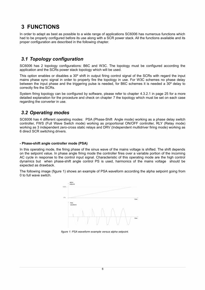
- Phase-shift angle controller mode (PSA)
In this operating mode, the firing phase of the sinus wave of the mains voltage is shifted. The shift dependson the setpoint value. In phase angle firing mode the controller fires over a variable portion of the incomingAC cycle in response to the control input signal. Characteristic of this operating mode are the high controldynamics but when phase-shift angle control PS is used, harmonics of the mains voltage should beexpected as drawback.
The following image (figure 1) shows an example of PSA waveform according the alpha setpoint going from0 to full wave switch.
6
figure 1: PSA waveform example versus alpha setpoint.
alphasetpoint
time
PSAwaveform
100%
0%time
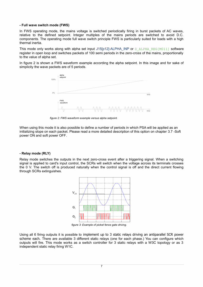
- Full wave switch mode (FWS)
In FWS operating mode, the mains voltage is switched periodically firing in burst packets of AC waves,relative to the defined setpoint. Integer multiples of the mains periods are switched to avoid D.C.components. The operating mode full wave switch principle FWS is particularly suited for loads with a highthermal inertia.
This mode only works along with alpha set input J15[p12]-ALPHA_INP or D_ALPHA_REG[M011] softwareregister in open loop and switches packets of 100 semi periods in the zero-cross of the mains, proportionallyto the value of alpha set.
In figure 2 is shown a FWS waveform example according the alpha setpoint. In this image and for sake ofsimplicity the wave packets are of 5 periods.
When using this mode it is also possible to define a number of periods in which PSA will be applied as an initializing slope on each packet. Please read a more detailed description of this option on chapter 3.7 -Soft power ON and soft power OFF.
- Relay mode (RLY)
Relay mode switches the outputs in the next zero-cross event after a triggering signal. When a switchingsignal is applied to card's input control, the SCRs will switch when the voltage across its terminals crossesthe 0 V. The switch off is produced naturally when the control signal is off and the direct current flowingthrough SCRs extinguishes.
Using all 6 firing outputs it is possible to implement up to 3 static relays driving an antiparallel SCR powerscheme each. There are available 3 different static relays (one for each phase.) You can configure whichoutputs will fire. This mode works as a switch controller for 3 static relays with a W3C topology or as 3independent static relay firing W1C.
7
figure 2: FWS waveform example versus alpha setpoint.
time
FWSwaveform
alphasetpoint
100%
0%time
figure 3: Example of picket fence gate driving.

Working as a relay mode the inputs voltage setpoint (J15[p15]-U_SETPOINT), current setpoint (J15[p14]-I_SETPOINT) and alpha setpoint (J16[p21]-ALPHA_INP) works as digital triggering inputs (according to itsconfiguration: TTL, 0-10 V, 0-20 mA or 4-20mA) and firing the outputs SCR1 & SCR2, SCR3 & SCR4, SCR5& SCR6 respectively.
System mode of operation can be configured by software, please refer to chapter 4.3.2.2 on page 26 for amore detailed explanation.
- Independent multidriver firing mode (DRV)
Independent multidrive mode switches the outputs according 6 independent triggering signals. When aswitching signal is applied to card's input control, SC6006 will switch ON the corresponding SCRs gate.
In this mode SC6006 will not sense the mains synchronism and acts just like 6 independent SCR drivers.
Fault signaling due synchronization and overcurrent will be disabled automatically in this operation mode aswell as the inhibit signal working as a source for Halt fault.
In independent multidriver firing mode the inputs current setpoint (J15[p14]-I_SETPOINT), voltage setpoint(J15[p15]-I_SETPOINT), current measure (J16[p19]-I_SENS), voltage measure(J16[p20]-U_SENS) andalpha setpoint (J16[p21]-ALPHA_INP) works as digital firing inputs (according to its configuration: TTL, 0-10V, 0-20 mA or 4-20mA) and firing the outputs SCR1,SCR2, SCR4, SCR5, SCR6 respectively.
Inhibit input (J15[p16]-INHIBIT) works as digital firing CMOS level input for SCR3.
System mode of operation can be configured by software, please refer to chapter 4.3.2.2 on page 26 for amore detailed explanation. An example of connection is given at chapter 7.4 on page 46.
8
3.3 Setpoint signals processingThere are 3 different analog input setpoints available: voltage setpoint (J15[p15]-U_SETPOINT), currentsetpoint (J15[p14]-I_SETPOINT) and alpha setpoint (J16[p21]-ALPHA_INP ), this signals works as externalreferences which should be provided by the operator or PLC to the controller (SC6006) giving thecorresponding setpoint when regulating the ouptut voltage of the converter, the output current of theconverter or the firing phase angle of the converter respectively.
As mentioned before all these input setpoint signals can be configured to work as 0-5 V or 0-10 V and also0-20 mA and live input 4-20 mA. This configurations are made using the PCB DIP switches and LCD screen.
Furthermore all this inputs can be digitally overrode. There are 3 software setpoint registers which can be setby the operator through LCD and push-buttons on board or by using the serial communication port.
3.3.1 Analog or digital references / setpoints
Input signals of current setpoint, voltage setpoint and alpha setpoint for the open or closed loop control canbe configured, independently, as a digital reference or analog reference.
If an input reference is set as digital, its value must be set through software using the on-board LCD menu orthrough RS-232 serial communications interface, the following are the corresponding software registers:
alpha_setpoint: D_ALPHA_REG[M011]
u_setpoint: D_VOLTAGE_REG[M034]
i_setpoint: D_CURRENT_REG[M035]
All the digital setpoint are 10 bits registers and can be set with decimal values from 0 to 1023.
Please refer to chapter 5-SERIAL COMMUNICATION for further explanation regarding the communicationsinterface and communications protocol of the system if it is needed to change this registers remotely.
If an input reference is set as analog the corresponding value is obtained by his assigned PCB input:
alpha_setpoint: J16[p21]-ALPHA_INP
u_setpoint: J15[p15]-U_SETPOINT
i_setpoint: J15[p14]-I_SETPOINT
Note: All analog setpoint input signals can be configured to work as 0-5 V or 0-10 V and also 0-20 mA. Additionally they can beinterfaced connecting a potentiometer (2 included). The recommended value of this potentiometers is 4.7 kΩ.
Configuration are made using the PCB DIP switches. Please refer to chapter 4.4.2 on page 31 for the DIP-switchesconfigurations.
Also all inputs can be configured as 4-20 mA (Live Input). The Live Input is enabled through software. Please refer tochapter 4.3.2.4 on page 26.
3.3.2 Setpoints signal processing diagrams
This chapter provides several simplified diagrams and blocks regarding the different sources of setpointsavailable with the aim of clarify the way this setpoints are processed and routed or selected by SC6006.
This diagrams depicts, when necessary, the input impedance or resistive charge for the input signal, thefiltering (low pass) and shaping modules (live input shaping) as well the hardware and software setting whichselects or switchs one or other signal path depending on selected signal source by the operator.
Please take them as a guidance planned for the sake of a more in-depth and comprehensive scheme of theSC6006 signal path and setpoint signal process.
9

Alpha setpoint signal processing.
In figure 4 is shown the diagram for acquisition and setting of alpha setpoint.
By default SC6006 takes the alpha setpoint from the analog ALPHA_INP input configured as 0-5 VDC.
Voltage setpoint signal processing.
In figure 5 is shown the diagram of acquisition and setting of voltage setpoint.
By default SC6006 takes the voltage setpoint from the analog U_SETPOINT input configured as 0-5 VDC.
Current setpoint signal processing.
In figure 6 is shown the diagram of acquisition and setting of current setpoint.
By default SC6006 takes the current setpoint from the analog I_SETPOINT input configured as 0-5 VDC.
10
figure 4: alpha setpoint signal processing diagram.
figure 5: Voltage setpoint signal processing diagram.
figure 6: Current setpoint signal processing diagram.
ADC
0-5V / 0-20mAU13-A 0-5V / 0-10V : U13-B
0-20/4-20mA : Live inp.
ALPHA: [An / Dig]
D_ALPHA_REG[M011] 1
0
ALPHA_REG[M005]
J16 18
J16 21
ALPHA_INP
J15 15
U_SETPOINT
0-5V / 0-20mAU11-C 0-5V / 0-10V : U11-D
0-20/4-20mA : Live inp.
VOLTAGE: [An / Dig]
D_UREF_REG[M012] 1
0
U_REF_REG[M008]
J15 13
ADC
J15 14
I_SETPOINT
0-5V / 0-20mAU11-A 0-5V / 0-10V : U11-B
0-20/4-20mA : Live inp.
CURRENT: [An / Dig]
D_IREF_REG[M013] 1
0
I_REF_REG[M009]
J15 13
ADC

3.4 Feedback signals processingSC6006 have 2 independent feedback signals: current feedback signal and voltage feedback signal. Thissignals are used when a closed loop control is needed.
As on the previous chapter, following, simplified diagrams are provided regarding the different sources offeedback signals available with the aim of clarify the way this feedback signals are processed and routed orselected by SC6006.
Current feedback signal processing.
There are 3 different analogic sources available for the current feedback signal:
• Current transformers: AC currents. The current feedback signal can be obtained directly fromstandard 200 mA AC current transformers (J14[p9..11]-I_AUX).
• Shunt: DC currents. By interfacing a standard 60 mV shunt (J14[p12]-I_SHUNT) .
• Analog configurable input: current feedback signal also can be obtained with an analog (0-5 V , 0-10V, 0-20 mA or 4-20 mA) current signal (J16[p19]-I_SENS).
The operator must choose and configure which source for current and voltage feedback signal wants to workwith according the application, the configuration of current feedback signal processing, filters and selectionor routing is as shown in figure 7.
By default SC6006 takes the current feedback signal from the analog I_SENS input configured as 0-5 Vsignal.
11
figure 7: Current feedback signal processing diagram.
IMEAS_REG[M007]ADC
J21
J22
J14 09
I_AUX
J14 10
J14 11
J15 14
I_SHUNT
0-60 mVJ15 13
J16 19
I_SENS
0-5V / 0-20mAU11-A 0-5V / 0-10V : U11-B
0-20/4-20mA : Live inp.J16 18
Voltage feedback signal processing.
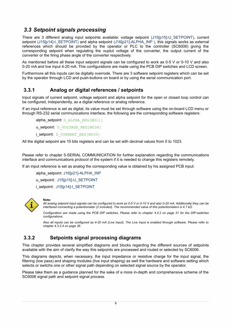
The voltage feedback signal can be obtained with direct output voltage connection (J12[p1]-V_REAL) or withan analog (0-5 V or 0-10 V and also 0-20 mA or 4-20 mA) voltage signal (J16[p20]-U_SENS). The operatormust ensure and configure which source for voltage feedback signal wants to be used in his application asshown in figure 8.
By default SC6006 takes the voltage feedback signal from the analog U_SENS input configured as 0-5 V.
3.5 Setpoints and feedback live input signals configurationAll inputs, setpoints and feedback signals, can be configured to work as 0-5 V or 0-10 V and also 0-20 mA.This configuration is made using the PCB DIP switches (chapter 4.4.2 on page 31).
Also all setpoint and feedback inputs can be configured as 4-20 mA (Live Input). The Live Input mode isenabled through software. How to set this option it is explained at chapter 4.3.2.4 on page 26.
3.6 Control ModesThe system can work with all its regulating operating modes (PSA and FWS) as open loop scheme settingthe output direct with alpha reference.
In PSA mode it is also possible to make a voltage and current regulation through a PID closed loop scheme.SC6006 has different control modes:
· OL: Open Loop control mode. Direct regulation of the output according alpha setpoint.
· V: Voltage feedback control. Voltage regulation of the output according voltage setpoint.
· I: Current feedback control. Current regulation of the output according current setpoint.
·IV: Both current and voltage feedback control. Voltage and current regulation of the outputaccording the most restrictive between current and voltage setpoints.
The control mode is set by software, please refer to chapter 4.3.2.5 on page 26 for further information abouthow to set the working control mode of the system.
12
figure 8: Voltage feedback signal processing diagram.
J20
UMEAS_REG[M006]ADC
J16 20
U_SENS
0-5V / 0-20mAU11-C 0-5V / 0-10V : U11-D
0-20/4-20mA : Live inp.J16 18
J12 01
U_REAL
J12 02
0-700 VDC
R01

3.7 Soft power ON and soft power OFF• Soft init slope and soft turn off slope for phase-shift mode (PSA)
When working in PSA mode SC6006 can operate making a soft power ON and soft power OFF. When softpower ON is set and the unit is started, the phase delay will be gradually decreased until it reaches thesetpoint. The soft power ON time can also be set by software.
Same way, when soft power off is set and the unit is being stop, the phase delay will be gradually increasedfrom the actual setpoint until it reaches the off state.
In the image is shown a soft power on from 0 to 100%.
The power on and the power off times can be set by software varying from 1 to 30 seconds, how to set thesoft power on and off and the timings is further explained in chapter 4.3.2.6 on page 26.
• Soft init slope and soft turn off slope for proportional mode (FWS). Avoiding transformer inrush current.
It is recommended to use this configuration in order to reduce the inrush current when controlling atransformer primary driving resistive loads on its secondary on proportional mode. When a transformer isfirst energized a high transient current can flow for several cycles due core saturation. Usually the worstcase inrush happens when the primary winding is connected at an instant around the zero-crossing of theprimary voltage as it occurs every starting period on each mains wave packet when operating in FWS mode.
The inrush current is greater than the nominal operating current of transformer and the ratio can vary from afew percent up to many times the operating current, this can blow up fuses and trip circuit breaker it alsocauses causes harmonics which can excite system resonances and cause dynamic overvoltage, all thiseffects may lead to the breakdown of the power equipment.
In many cases a single period (1st period of the pulse train) fired at 90º will suffice to reduce to its minimumthe inrush peak. In other cases a specific number periods of soft on would reduce at its maximum the initialinrush current. A recommendation would be to initially set a single cycle of soft turn on, monitorize the initialpeak current and compare it with different number of cycles and select the most suitable for the application.
On figure 10 is depicted as example the initial transient on each packet working with FWS with 5 cycles ofPSA soft init. In this image and for sake of simplicity the wave packets are of 7 periods.
You can find more information regarding the procedure to configure SC6006 to operate with this firing mode in chapter 4.3.2.6 Soft ON/OFF ramps submenu on page 26 of this manual.
13
figure 9: PSA soft power on waveform example.
alphasetpoint
time
PSAwaveform
100%
0%time
figure 10: Pulse train example with a soft init on FWS mode.

3.8 Fault sources and pulse inhibitionWhen the system is in ON state, the output pulse inhibition it is produced when an enabled fault source inworking condition occurs.
There are 3 different sources that triggers a fault: incorrect mains sync or rotation, external blocking signalthrough an external logic inhibit signal or contact block signal and overcurrrent condition.
All this fault conditions can be masked through software or some of them modified. The triggering of faultsignal is made as it is shown in diagram on figure 11.
Sync signal: When unmasked, it is triggered when the phase rotation of mains is reversed than theconfigured one or triggered when mains is out of sync, for example by its disconnection or by thedisconnection or out of phasing of one of its phases.
Halt signal: When unmasked, it is triggered when inhibition input (J15[p16]-INHIBIT) or block input (J13[p6]-BLK) switches on activation state given by signals en_inh and en_ext_blq set by software (chapter 4.3.2.7on page 27).
OvCurr signal: When unmasked, it is triggered when the measured feedback current exceeds the maximumset by OV_CURRENT_REG[M036].
When any of this 3 fault signals is triggered and fault generation is enabled, a fault condition will occur andwill stop (if it is in working state) the system and set the fault fault flags, those are visible in main menu of on-board display and with signaling LEDs.
The fault condition will be reset when all fault signals returns to OFF state. Then the system can be triggeredON again or, if it is set this way, it will resume its previous operation mode.
Output fault dry relay
When fault condition occurs and sets fault signal the output dry relay will be triggered ON following the faultsignal. User can use this output to externally detect and properly set its PLC or uP control system to actaccording when a fault is produced.
Fault interlock
SC6006 can interlock a fault condition by using its interlock function. When fault interlock mode is enabled(see chapter 4.3.2.7 in page 27.) any fault signal will stop the firing mode, and the system will not resume itsprevious working and release the fault state mode until all the fault sources are deactivated again and thesystem put on OFF state by pressing [OK] push-button on the main menu.
14
figure 11: Logic diagram for fault signal.
: SETTABLE CONF. BIT
: INTERNAL STATE
sync_bit
halt_bit
ov_curr_bit
EN_EXT_BLQ
BLQ
EN_INH
INHEN_HALT
EN_SYNC
SYNC
EN_OV_CURR
OV_CURR
EN_FAULT
FAULT
3.9 Start up modeUsing the start up setting SC6006 can be configured to, when powered on, start in ON mode, OFF mode orremembering the last state before it was powered down. By default the unit is configured to start up with thelast system state. This option is software set (chapter 4.3.2.8 on page 27).
3.10 Autoset function
Autoset function SC6006 automatically checks the mains frequency mode, the SCR output assignation andthe phase rotation. By default Autoset function is executed automatically every SC6006 startup, but user canmask or unmask which properties will set up this function. All its options can be software configured. Also,Autoset function can be triggered by software in any moment with no need to turn on and off the system. Seechapter 4.3.2.9 on page 28.
Note: When powered on, SC6006 automatically starts the autoset function before initialize all the system. So, in order to workproperly all the power system must be connected and powered on at the same time or before power on the SC6006.Otherwise the Autoset function would be unable to determine the frequency of mains or rotation or output assignationand will be configured in a default mode or with the previous detected configuration.
Mains frequency configuration:
By default every time the board is powered up checks the mains frequency mode (50 Hz or 60 Hz) and thenit can automatically configure itself to work at the corresponding mains frequency. The operator can alsomask this option and manually set through software the frequency of operation.
Mains frequency autodetect option can be masked and configured by software:
SUBMENU 1.8: AUTOSET > AC freq > [Auto/50Hz/60Hz]
If the mains frequency autoset is enabled but during the autoset process the system cannot determine it, theworking frequency will be set the same as the last time used.
Phase rotation autoset:
SC6006 can autodetect and correct a change in phase rotation. This occurs when, in the mains, 2 phaseswere swapped (e.g.: S and T swaps yelding R-S-T → R-T-S).
Phase rotation autodetect option can be masked and configured by software:
SUBMENU 1.8: AUTOSET > Rotation > [Auto/CW/ACW]
By default phase rotation autoset is executed automatically every SC6006 startup and checks if there is anychange since the last configuration. If there is any change the system autoconfigures itself. Thisautoconfiguration can also be masked.
If the phase rotation autoset is enabled but during the autoset process the system cannot determine it, thephase rotation will be set the same as the last time used.
SCRs automatic output assignation:
SC6006 can autodetect how the SCRs has been connected to the PCB and autoconfigure correctly thecorresponding output signals.
The SCRs automatic assignation detects and corrects the output signal assignation scheme in the followingcases:
– A swap between the SCRs in a same branch (W3C or B6C) or module. e.g. : SCR1 ↔ SCR2.
– A swap between 2 pairs of SCRs of different branches or between 2 modules. E. g. : SCR1 ↔SCR3 and SCR2 ↔ SCR4.
15

If the operator wants to use this option SC6006 must be connected to a resistive load in B6C scheme, and ina delta or wye resistive load in W3C. It is also recommended to connect the neutral.
In some cases outputs autoset may be unable to find the correct outputs assignation and, by default willdisable all the outputs (0). The user can override the automatic configuration by manually setting up theoutput assignation.
SCRs output assignation option can be disabled and configured by software:
SUBMENU 1.8: AUTOSET > Outputs > [No/Auto]
By default outputs autoset is disabled. Can be useful to use this function when installing the power stack thefirst time to get a quick and easy configuration and, then, save the configuration and disabling the outputsautoset mode.
If the automatic outputs detection in autoset is enabled but during the autoset process the system cannotdetermine it, the outputs assignation will be the same as the last time was saved in EEPROM.
Note: The SCRs automatic assignation option works only for W3C and B6C schemes with resistive loads. For other topologiesthe user must leave disabled the outputs autoset option and configure the system according the SCRs connectionscheme through SUBMENU 1.9: OUTPUTS.
3.11 Output assignation optionEach output of the SC6006 can be software set independently to operate according R, S, or T phase and forthe positive semi-cycle (r,s,t) or the negative semi-cycle (r',s',t'). Also can be permanently disabled (0).
The output assignation option is found at:
SUBMENU 1.9: OUTPUTS
Please refer to chapter 7 on page 41 for the standard topologies and its corresponding outputs configuration.
3.12 Saving all the changes and configurationsWhen the operator has made some settings change or properly configured all the options of the system thenew configuration must be saved in the internal EEPROM through:
SUBMENU 1.11: SAVE > [OK]
All changes not properly saved in the EEPROM will be lost during a power down and the previous EEPROMsaved configuration will be restored in the next power up of the system.
Note: Remember to save the configurations to the internal EEPROM every time a change is made or all the changes will belost when system is powered off.
3.13 Restore default configurationsThe factory default software configurations of the system can be restored at any moment using the menuoption:
SUBMENU 1.12: RESTORE > [OK]
When restored, the system will be automatically rebooted and all software configurations back to defaultfactory set.
16
4 SETTINGS AND OPERATIONIn this chapter is given a complete device overview, with a description of all available input/output signalsand connections available and a brief description of all software options and on-board hardwareconfigurations made by jumpers and DIP-switches.
4.1 PCB connectors overview
17
figure 12: Connectors PCB overview.
table 1: List of connectors and pinning.
Terminal Name Description Terminal Name Description
J1AC_IN1 AC / DC power supply input.
J14
8 GND Signal ground.
AC_IN2 AC / DC power supply input. 9 AUX_I_R R phase input for CT.
J11
R R_SYNCH Mains R phase input. 10 AUX_I_S S phase input for CT.
S S_SYNCH Mains S phase input. 11 AUX_I_T T phase input for CT
T T_SYNCH Mains T phase input. 12 I_SHUNT Shunt input terminal.
N NEUTRAL Mains neutral input.
J15
13 GND Signal ground.
J121 V_REAL Direct voltage input feedback. 14 I_SETPOINT Input current setpoint.
2 GND Signal ground. 15 U_SETPOINT Input voltage setpoint.
J13
3 K1_NC Output dry relay N/C contact. 16 INHIBIT inhibit input signal.
4 K1_COM Output dry relay COM contact. 17 VCC +5 VDC output reference.
5 K1_NO Output dry relay N/O contact.
J16
18 GND Signal ground.
6 BLK Blocking signal input. 19 I_SENS Input current feedback.
7 VDD +15 VDC from SC6006. 20 U_SENS Input voltage feedback.
21 ALPHA_INP Input alpha setpoint.
22 VDD +15 VDC from SC6006.
3 8 9 10 11 12 13 14 15 16 17 18 19 20 214 5 6 7 22
N RST
PWR
RESET
EXT BLKOV CURRFAULTFIRING
SC6006
G6 K6K5G5K4G4K3G3K2G2K1G1
MENU OK
ALPHAU_SENSI_SENSU_SETI_SETI_SENSU_SENS
LC
D C
ON
TR
AS
T
COARSE FINE
1 2
J11 - SYNCHRONISMCONNECTOR
OUTPUT SCR FIRINGCONNECTORS
SIGNALING LEDS
J32 - DB-9 (DCE) RS-232COM CONNECTOR
J16 - FEEDBACK ANDALPHA SETPOINT
J15 - SETPOINTSAND INHIBIT
J14 - CURRENTINPUT FEEDBACK
J13 - EXTERNAL BLOCKAND DRY OUTPUT FAULT
J12 - FEEDBACKVOLTAGE
J1 - POWERSUPPLY
SE
MIC
OD
EE
LE
CT
RO
NIC
A
®
SC
60
06
4.2 ConnectorsFollowing is listed and described every connector and every output/input signal available of the SC6006.
4.2.1 Power supply connector (J1)
Connector J1 is the input mains supply connection for the switched mode power supply on board.
The system can be powered with AC (or DC) power source from 195 VAC to 480 VAC. For more technicaldetails or maximum and recommended values and parameters please refer to chapter: 10-TECHNICALSPECIFICATIONS.
The connector type is a MSTBVA series (or equivalent) from Phoenix Contact (ref. MSTBVA2,5/3-G-5,08).The board is also provided with the matching plug connector (ref. MSTB2,5/3-ST-5,08).
4.2.2 Synchronism connector (J11)
Synchronism connector is labelled (PCB silkscreen) indicating the three phases R, S, T and neutral N. Mainsconnection must guarantee concordance with the SCRs to get sure that the synchronism and phase rotationis correct. If the concordance is wrong this can be fixed without reconnecting the SCRs by means Autoset function ormanually assigning the correct outputs by software.In case the phase rotation is wrong the PCB can autodetect and solve it using the Autoset function or, if it isenabled phase rotation autoset during the power on, just by reset the system.
The connector type is an MSTBA series (or equivalent) from Phoenix Contact (ref. MSTBA 2,5/7-G-5,08).The board is also provided with the matching plug connector (ref. MSTB 2,5/7-ST-5,08).
18
figure 13: Detail of mains supply input connector.
figure 14: Detail of sync input connector.
J1
J11
4.2.3 Feedback voltage signal connector (J12)
Direct voltage feedback input is made on J12 connector. Please note that in those cases where controlboard is controlled by external equipments, like PLC, microcontrollers, etc, without isolated outputs, it mustbe considered to have all the feedback elements isolated. Using elements like shunts to close the currentloop, and voltage feedback could not be done directly if galvanic isolation is required.There are available isolated feedback modules designed to work with this control board. Please see chapter 8 -AVAILABLE ACCESSORIES on page 50 for a list and explanation of suitable accessories for SC6006.
- J12 PINOUT:• Terminal 1 (V_REAL): Direct voltage input feedback signal.• Terminal 2 (GND): PCB signal ground.
The connector type is an MSTBVA series (or equivalent) from Phoenix Contact (ref. MSTBVA2,5/3-G-5,08).The board is also provided with the matching plug connector (ref. MSTB2,5/3-ST-5,08).
4.2.4 External block and dry output fault connector (J13)
The external block connector and dry output fault connector provides the user an input blocking signal (usingfor example an external contactor or switch) and an output dry relay for fault signaling.
- J13 PINOUT:• Terminal 3 (K_NC): Output dry relay N/C contact.• Terminal 4 (K_COM): Output dry relay COM contact.• Terminal 5 (K_NO): Output dry relay N/O contact.• Terminal 6 (BLQ): Input terminal of the blocking signal.• Terminal 7 (VDD): Positive terminal blocking signal (15 VDC).(*)
(*) please do not use this terminal to power other external devices. Refer to ELECTRICAL CHARACTERISTICS TABLE for furtherinformation.
Terminal 6 (BLQ) must be shortcircuited with Terminal 7 (VDD) for trigger ON the input blocking signal.
Terminals 3-5 are those corresponding to the dry output fault relay. Relay switches ON (Terminal 4connected with Terminal 5) when fault occurs. Otherwise, if there is no fault, relay switchs OFF (Terminal 4connected with Terminal 3). Please see the connection diagram for J13 in figure 15.
19
figure 15: Connection example diagram for J13.
8 92 3 4 5 6 7
external blockswitch
K1
output faultsignaling relay
J12
J13
The J13 connector type is an MCV series (or equivalent) from Phoenix Contact (ref. 1803442). SC6006 isalso provided with the matching plug connector (ref. 1803604).
Note: By default SC6006 is configured to operate with a normally-off blocking contactor. To work without the blocking mode orwith a normally-on contact you must set this option through software. Please see chapter 4.3.2.7 in page 27.
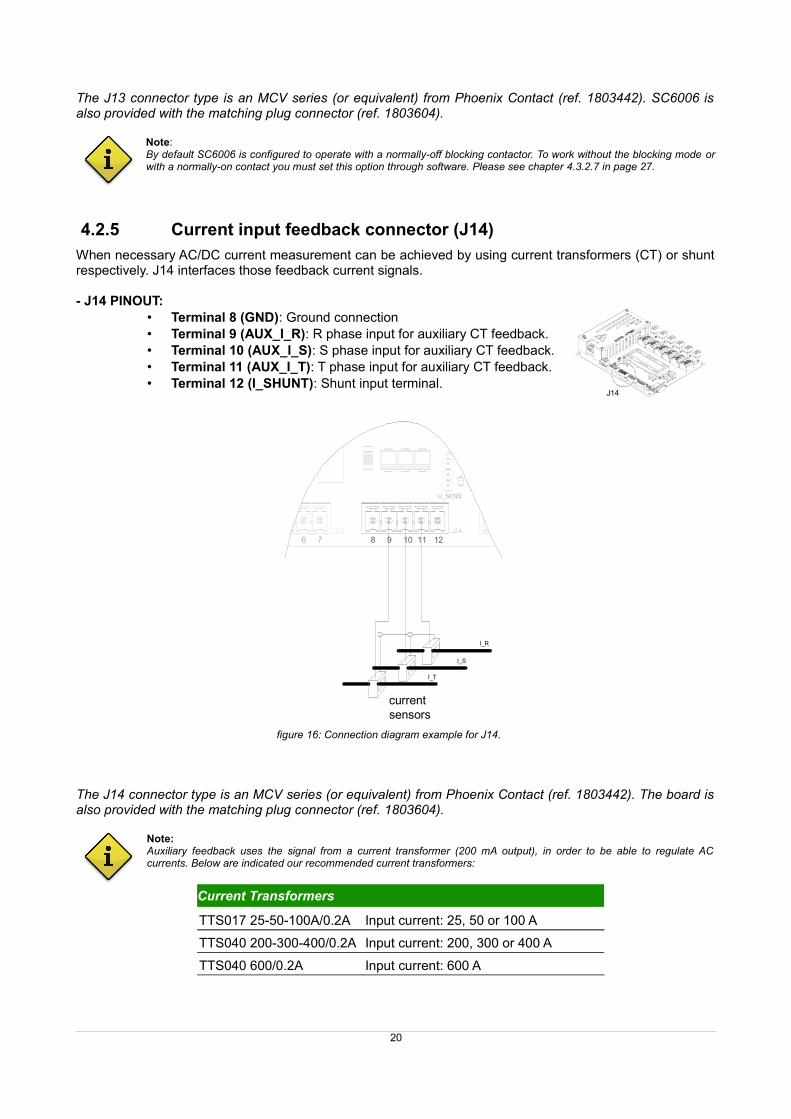
4.2.5 Current input feedback connector (J14)
When necessary AC/DC current measurement can be achieved by using current transformers (CT) or shuntrespectively. J14 interfaces those feedback current signals.
- J14 PINOUT:• Terminal 8 (GND): Ground connection• Terminal 9 (AUX_I_R): R phase input for auxiliary CT feedback.• Terminal 10 (AUX_I_S): S phase input for auxiliary CT feedback.• Terminal 11 (AUX_I_T): T phase input for auxiliary CT feedback.• Terminal 12 (I_SHUNT): Shunt input terminal.
The J14 connector type is an MCV series (or equivalent) from Phoenix Contact (ref. 1803442). The board isalso provided with the matching plug connector (ref. 1803604).
Note: Auxiliary feedback uses the signal from a current transformer (200 mA output), in order to be able to regulate ACcurrents. Below are indicated our recommended current transformers:
Current Transformers
TTS017 25-50-100A/0.2A Input current: 25, 50 or 100 A
TTS040 200-300-400/0.2A Input current: 200, 300 or 400 A
TTS040 600/0.2A Input current: 600 A
20
figure 16: Connection diagram example for J14.
8 9 10 11 126 7
U_SENS
currentsensors
I_R
I_S
I_T
J14
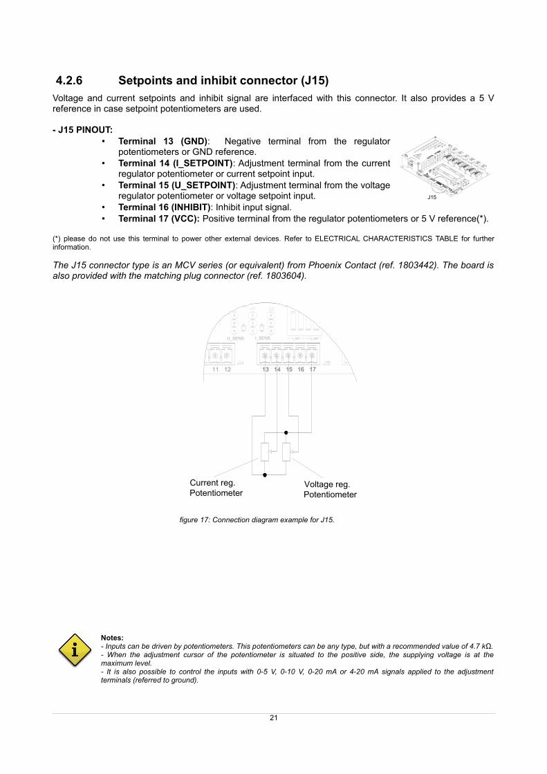
4.2.6 Setpoints and inhibit connector (J15)
Voltage and current setpoints and inhibit signal are interfaced with this connector. It also provides a 5 Vreference in case setpoint potentiometers are used.
- J15 PINOUT:• Terminal 13 (GND): Negative terminal from the regulator
potentiometers or GND reference.• Terminal 14 (I_SETPOINT): Adjustment terminal from the current
regulator potentiometer or current setpoint input.• Terminal 15 (U_SETPOINT): Adjustment terminal from the voltage
regulator potentiometer or voltage setpoint input.• Terminal 16 (INHIBIT): Inhibit input signal.• Terminal 17 (VCC): Positive terminal from the regulator potentiometers or 5 V reference(*).
(*) please do not use this terminal to power other external devices. Refer to ELECTRICAL CHARACTERISTICS TABLE for furtherinformation.
The J15 connector type is an MCV series (or equivalent) from Phoenix Contact (ref. 1803442). The board isalso provided with the matching plug connector (ref. 1803604).
Notes:- Inputs can be driven by potentiometers. This potentiometers can be any type, but with a recommended value of 4.7 kΩ.- When the adjustment cursor of the potentiometer is situated to the positive side, the supplying voltage is at themaximum level.- It is also possible to control the inputs with 0-5 V, 0-10 V, 0-20 mA or 4-20 mA signals applied to the adjustmentterminals (referred to ground).
21
figure 17: Connection diagram example for J15.
Current reg.Potentiometer
Voltage reg.Potentiometer
11 12 13 14 15 16 17
U_SETI_SETI_SENSU_SENS
11 12
J15

4.2.7 Feedback and alpha setpoint input connector (J16)
Voltage and current feedback signals and alpha setpoint signal are interfaced with this connector.
- J16 PINOUT:• Terminal 18 (GND): Negative terminal from the regulator
potentiometers or GND reference.• Terminal 19 (I_SENS): Current feedback signal input.• Terminal 20 (U_SENS): Voltage feedback signal input.• Terminal 21 (ALPHA_INP): Alpha reference input.• Terminal 22 (VDD): Positive terminal from 15 V reference(*).
(*) please do not use this terminal to power other external devices. Refer to ELECTRICAL CHARACTERISTICS TABLE for furtherinformation.
The J16 connector type is an MCV series (or equivalent) from Phoenix Contact (ref. 1803442). The board isalso provided with the matching plug connector (ref. 1803604).
Notes:- ALPHA_INP setpoint can be driven by a potentiometer. This potentiometer can be any type, but with a recommendedvalue of 4.7 kΩ. If a potentiometer is used its positive +5 VDC reference can be wired to J15:17 (VCC) and GNDreference to J16:18 (GND).I_SENS, U_SENS and ALPHA_INP can work with 0-5 V, 0-10 V, 0-20 mA or 4-20 mA signals level.
22
figure 18: Connection diagram example for J16.
Currentsensor
Voltagesensor
18 19 20 21 22
ALPHAU_SENSI_SENS
COM GND
+5 VDC
SCRs POWER STACK
Alpha reg.Potentiometer
J16

4.2.8 Output SCR firing connectors (SCR1-SCR6)
The output SCR firing connectors are labelled (PCB silkscreen) indicating the six outputs SCR1 to SCR6and its correspondent G and K connections, please see figure 19. Mains connection must guaranteeconcordance with the SCRs to get sure that the synchronism and phase rotation is correct. If the concordance is wrong this can be fixed without reconnecting the SCRs by means Autoset function ormanually assigning the correct outputs by software.In case the phase rotation is wrong the PCB can autodetect and solve it using the Autoset function or, if it isenabled phase rotation autoset during the power on, just by reset the system.
Connector Gate Cathode
SCR1 G1 K1
SCR2 G2 K2
SCR3 G3 K3
SCR4 G4 K4
SCR5 G5 K5
SCR6 G6 K6
The connectors type is an MSTBVA series (or equivalent) from Phoenix Contact (ref. 1755736). The board isalso provided with the matching plug connectors (ref. 1757019).
Notes:- For thyristor connection, see chapter 7 where there are the most typical circuits. And please read the mountingrecommendations on page 48, - Avoid long cables in the firing system, and always use twisted or shielded cables (preferred).
4.2.9 Serial communications DB-9 connector (J32)
The connector type is a specific DB-9 male (DTE) connector.Can be interfaced to a standard PC serial port or PLC RS232port.
Please check chapter 5 -SERIAL COMMUNICATION on pagefor a more detailed information regarding te use of the SC6006serial communication port.
23
figure 19: Detail of output SCR firing connectors.
N RST G6 K6K5G5K4G4K3G3K2G2K1G1
TO SCRs (SCR1-SCR6)
SCR6SCR5
SCR4SCR3
SCR2SCR1
J32

4.3 LCD menu settings and navigationSC6006 has an on-board integrated alphanumeric LCD that provides an user interface to easy set up andmonitor every configuration or setting of the system.When initializes SC6006 starts on main menu as is shown in figure 20 and there are a total of 3 menus. Themain menu (on top of the figure), settings menu, and registers menu. User can go cyclically through thismenus clicking the [MENU] push-button.
The [OK] push button triggers ON the SCR controller when its pushed at main menu and accepts theintroduced changes or access to the submenus when it's pressed in the other menus.The [UP] an [DOWN] push buttons move up and down in the menus and, when selected, increases ordecreases the settings variables.
4.3.1 Main Menu:
In the main menu you can see in a glimpse the actual state of the system. – Faults: If there is any fault condition it will appear “FLT!” at the left LCD corner.– ON/OFF system status. At the right LCD corner.– Halt (H), sync (S) and overcurrent (I) fault flags.– Voltage and current setpoint references or alpha reference.– Voltage and current measurements.– Firmware version.
By default SC6006 will show in the first line of main menu its version and if there is any fault. In the secondline the values (in %) of the reference inputs (current and voltage).By pressing the push-button [UP] the first line of main menu will switch to the default information to show the
24
figure 21: Detail of main menu in LCD display.
figure 20: menu sequence of SC6006.
SETTINGS MENUREGISTERS MENU
[MENU]
[MENU]
[MENU]
fault mode sign halt and synch flags firmware version
voltage setpoint current setpoint ON/OFF system status
PWR
RESET
EXT BLKOV CURR
FAULTFIRING
MENU OK

actual values (in %) of the sensed current and voltage. If the SC6006 is in fault mode then the first linealways will show the default information.By pressing the push-button [DOWN] the second line of the main menu will switch to the default informationto show the actual value (in %) of the alpha reference.When during the initialization SC6006 could not determine the phase-rotation, frequency or outputassignation and its default configuration it is ben made a “!” character will be shown on the fist position of thesecond line.
4.3.1.1 LCD contrast adjusting potentiometerBy means the potentiometer P5 (see figure 22) operator or user can readjust the contrast of LCD in casemore or less contrast is needed according the environmental light or visual conditions. The contrast is in factory adjusted for an optimal LCD reading.
4.3.1.2 LCD backlightWhen SC6006 is in the main menu you can switch the LCD backlight OFF by pressing and hold for a secondthe push-button [DW].The LCD backlight can be turned ON again by pressing and hold for a second the push-button [UP].By default LCD backlight is ON.
Note:All the changes of visualization, information and backlight state introduced in the main menu can be saved in EEPROMby submenu 1.11 (submenu save).
4.3.2 Settings menu
In settings menu it is possible to change all the internal characteristics and modesof operation of the system. We can access this menu pressing [MENU] push-button when we are in main menu.
4.3.2.1 Topology option
MENU 1: SETTINGS > Topology > [B6C / W3C]
By pressing [OK] button we can change between B6C topology and W3C topology operation.
By default SC6006 is configured in W3C topology.
25
figure 22: P5 LCD contrast adjusting potentiometer
3 8 9 10 11 12 13 14 15 16 17 18 19 20 214 5 6 7 22
N RST
PWR
RESET
EXT BLKOV CURR
FAULTFIRING
SC6006
G6 K6K5G5K4G4K3G3K2G2K1G1
MENU OK
ALPHAU_SE NSI_S ENSU _SE TI_ SETI_SENSU_SENS
LCD
CO
NT
RA
ST
COARSE FINE
1 2
SC
600
6
TOPOLOGY OPTION
SETTINGS MENU

4.3.2.2 Mode option
MENU 1: SETTINGS > Mode > [PSA / FWS / RLY / DRV]
By pressing [OK] button we can change between PSA, FWS, RLY and DRV modes of operation.
By default SC6006 is configured in PSA mode.
4.3.2.3 Reference submenu
SUBMENU 1.2: REFERENCE > alpha > [An / Dig]
> voltage > [An / Dig]
> current > [An / Dig]
By pressing [OK] button we access to the Reference submenu. In this submenu we can change thereferences which SC6006 uses to calculate the setpoint. It is possible to choose between analog referencesfor alpha, voltage and current or use the digital registers for this setpoints . By default SC6006 is configured with all of its inputs as analog references.
4.3.2.4 Live-zero input submenu
SUBMENU 1.3: INPUTS > i_ref > [0 mA/ 4 mA]
> i_meas > [0 mA/ 4 mA]
> u_ref > [0 mA/ 4 mA]
> u_meas > [0 mA/ 4 mA]
> alpha_inp > [0 mA/ 4 mA]
By pressing [OK] button we access to the Live-inputs submenu. In this submenu we can set each inputworking as a normal input or as live input (4-20 mA). Please note that the DIP-Switches configuration mustbe set according the voltage or current levels required.
By default all inputs in SC6006 are configured in zero mode (no live-input).
4.3.2.5 Control option
MENU 1: SETTINGS > Control > [OL / I / V / IV]
By pressing [OK] button system changes between “OL” (open loop), “I” (current regulation), “V” (voltageregulation) or “IV” (both current and voltage regulation).
By default SC6006 is configured in OL mode.
4.3.2.6 Soft ON/OFF ramps submenu
SUBMENU 1.6: ON/OFF Ramps > Soft ON > [OFF / ON]
> Time ON > [1..30]s/c(+ -)
> Soft OFF > [OFF / ON]
> Time OFF > [1..30]s/c(+ -)
26
MODE OPTION
REFERENCE SUBMENU
LIVE INPUT SUBMENU
CONTROL OPTION
ON/OFF RAMPS SUBMENU
• When SC6006 is operating on PSA Mode:
By pressing [OK] button it access to the Soft ON/OFF ramps submenu. In this submenu you can activate ordeactivate the soft turn on and soft turn off and set up the both times.
By default SC6006 is configured with 10 seconds (both UP and DOWN) ramps but with soft on and offoptions disabled.
• When SC6006 is operating on FWS Mode:
By pressing [OK] button it access to the Soft ON/OFF ramps submenu. In this submenu you can activate ordeactivate the soft turn on and soft turn off on FWS mode and set up the both number of cycles in whichPSA will be used.
By default SC6006 is configured with 10 cycles (both UP and DOWN) ramps but with soft on and off optionsdisabled.
Note:On cases where a determinated number of cycles of turn on is set, the minimum firing packet will be this number ofcycles A. On those cases where a determinated number of cycles B of turn off where set the minimum firing packet willbe B. On those cases where turn on and turn off is set with A and B cycles respectively the minimum firing packet will beA+B cycles. Additionally, if alpha setpoint is set to 0% SC6006 will not fire, alternatively if alpha setpoint is set to 100%
the board will be permanently activated ignoring turn on and turn off clycles.
4.3.2.7 Faults submenu
SUBMENU 1.7: Faults > Blq > [N.OFF / N.ON]
> Inh > [N.OFF / N.ON]
> Halt > [En / Dis]
> Sync > [En / Dis]
> OvCurr > [En / Dis]
> Fault > [En / Dis]
> Interlock > [En / Dis]
In this submenu we can enable or disable each one of the sources of fault (Halt, Sync and OvCurr) and eventhe fault signal itself (Fault). We also can set if the signals block and inhibit works as a normally-on ornormally-off signals. Besides, the last option in submenu (Lock fault) interlocks the fault signal in case of faultevent and stops the system and blocks it until all faults are gone and the SC6006 is in OFF mode bypressing [OK] push button in main menu.
By default SC6006 is configured with all the faults enabled and block and inhibit signals normally off.Interlock fault disabled.
4.3.2.8 Start up option
MENU 1: SETTINGS > StartUp > [OFF / ON / Last]
By pressing [OK] button we can change between ON, OFF or Last state. Mode “ON” enables the firing every time the system is powered up. Mode “OFF” starts always SC6006stopped. In “Last state” mode starts the system maintaining the last state when it was powered down.
27
FAULTS SUBMENU
START UP OPTION

By default SC6006 is configured with LAST state when start up the system.
4.3.2.9 Autoset options submenu
SUBMENU 1.9: Autoset > AC Freq > [50Hz / 60Hz / Auto]
> Outputs > [No / Auto]
> Rotation > [No / Auto]
> Autoset?
By pressing [OK] button we access to the Autoset submenu. In this submenu we can configure the mainsfrequency (50 or 60 Hz) or leave the SC6006 finds by itself the working frequency. Also SC6006 can set upby itself the outputs configuration and the phase rotation.With the last option the SC6006 will start the autoset procedure. The autoset is launched every time the system is powered on autosetting the enabled configurations.
By default SC6006 is configured as 50 Hz mains frequency with the outputs detect disabled and automaticrotation enabled.
4.3.2.10 Outputs assignation submenu
SUBMENU 1.10: Outputs > SCR1 > [0 / r / r' / s / s' / t / t' / 1] (+ -)
> SCR2 > [0 / r / r' / s / s' / t / t' / 1] (+ -)
> SCR3 > [0 / r / r' / s / s' / t / t' / 1] (+ -)
> SCR4 > [0 / r / r' / s / s' / t / t' / 1] (+ -)
> SCR5 > [0 / r / r' / s / s' / t / t' / 1] (+ -)
> SCR6 > [0 / r / r' / s / s' / t / t' / 1] (+ -)
By pressing [UP] and [DOWN] we can select the SCRs outputs phase assignation. Pressing [OK] and thenUP] and [DOWN] we can move through each phase and assign the output SCR.
By default SC6006 outputs are configured as: r – r ' – s – s' – t – t'.r: meaning this output will switch during the positive semi-cycle of R-phase.r': meaning its output will switch during the negative semi-cycle of R-phase, and similarly for the
other phases.
4.3.2.11 Communications submenu
SUBMENU 1.9: COM > RS232 > [En / Dis]> Remote > [En / Dis]
By pressing [OK] in “RS232” option we can activate or deactivate the serial communication of the unit.
By pressing [OK] in “Remote” option we can activate or deactivate the serial communication of the unit whenoperating with a SCRP6006 remote panel please read on chapter 8.1 - SCRP6006 for further information.
By default SC6006 is configured with its serial port activated and the communication with a SCRP6006deactivated.
4.3.2.12 Save changes option
SUBMENU 1.10: Save all?
By pressing [OK] in “Save all?” a warning message will be displayed and then, if we push another time [OK]
28
AUTOSET SUBMENU
COMMUNICATIONS SUBMENU
SAVE CHANGES

all changes introduced will be saved in the internal EEPROM. By pressing [MENU] we will return to previousmenu.
4.3.2.13 Restore option
SUBMENU 1.10: Restore?
By pressing [OK] in “Restore?” a warning message will be displayed and then, if we push another time [OK]all configurations will be restored to the factory settings and then the controller rebooted.
4.3.3 Registers menu
In this menu it is possible to read and change some of the internal registers asdigital setpoints or frequency and duty cycle of the train pulse of the SCRs.The registers can be highlighted with [UP] and [DOWN] push-buttons, selected bypressing [OK] and then using [UP] and [DOWN] we can adjust, manually, itsvalues.Next will be briefly explained each of this set registers.
Digital setpoints registers> alpha_d: This is the corresponding digital register to adjust the alpha setpoint when the unit is
configurated to operate with the digital alpha setpoint register. This is a 10 bit register and can be set from 0 (0%) to 1023 (100%).
> uref_d: This is the corresponding digital register to adjust the voltage setpoint when the unit isconfigurated to operate with the digital voltage setpoint register. This is a 10 bit register and can be set from 0 (0%) to 1023 (100%).
> iref_d: This is the corresponding digital register to adjust the current setpoint when the unit isconfigurated to operate with the digital current setpoint register. This is a 10 bit register and can be set from 0 (0%) to 1023 (100%).
By default all digital setpoints registers are set to 0.
Overcurrent threshold register> o_curr: This register adjust the maximum rate of overcurrent when the overcurrent fault signal
is triggered.The o_curr register can be manually set from 50% to 300% of the measured input current with steps of 50%.
By default overcurrent register is set to 200%.
Output pulse gate train registers> fsw: This register adjust the switching frequency for the output pulse gate train. Can be set from
1 to 25 kHz and by default it is set for a frequency of 12 kHz.
> duty: This register adjust the duty cycle for the output pulse gate train. Can be set from 5% to30% and by default it is set for a duty of 25%.
Topology sync delay registers> dly1: This register adjust the firing delay when W3C topology is used. It is, by default,
configured to adjust the firing signal to the mains signal and normally there is no need to change its value.
> dly2: This register adjust the firing delay when B6C topology is used. It is, by default, configuredto adjust the firing signal to the mains signal and normally there is no need to change its value.
29
RESTORE CHANGES
REGISTERS MENU

4.3.4 Debug menu
If, when power on the SC6006, we maintain pressed the [UP] push-button we will enter in debug mode. Inthis mode we can access to another menu called debug menu. In this menu we can see with the on boardLCD the values of many internal registers of the system. This mode is intended only for debug purposes.
Note: All configuration changes introduced by user must be saved before power down or resetting the equipment or allchanges will be lost.
4.4 Jumpers and DIP Switches configurationsThere are some configurations that can not set in software and must be set using the jumpers and DIPswitches of the board. Following you will find an explanation of all the configurations set by jumpers and DIPswitches.
4.4.1 Jumpers J7 and J20 to J24
Jumpers allow to configure the different input options of the control board. In table below, there are indicatedthe possible jumper configuration options.
Jumper Description
J7 Used to control the gain of the direct voltage feedback input. Further description in 4.4.3.
JP20Used to change the source of voltage feedback signal between direct voltage feedback inputand analog input voltage signal input.
JP21 Used to select between auxiliary current transformers or shunt.
JP22Used to change the source of current feedback signal between auxiliary current transformers orshunt and analog input current signal input.
JP23It will be used for feedback with shunt in positive terminal and inverted voltage feedback. Seechapter 7.3.2 on page 44.
JP24 Do not use this jumper, leave all its pins unconnected.
Notes:In case of using an isolated sensor for the DC current feedback with J16[p19]-I_SENS, please double checkthe measuring direction of the sensor. Current feedback signal must be always positive.
In the following table can find the correct jumper configuration for common application schemes.
APPLICATION JP20 JP21 JP22 JP23
Rectifier (shunt + controlled) UP UP UP UPRectifier (shunt - controlled) UP UP UP DWAC control (aux. feedback) UP DW UP DWExternal voltage and current control DW DW DW DWFeedback by SCCAVO2 OA UP DW DW DW
Warning notes:- Make sure and double check the position of the plugging connectors (jumpers), following previous indications.- JP70 and JP71 are reserved, do not use them, they always must be connected.- Do not let any jumper unconnected except for the J24 jumper.
30
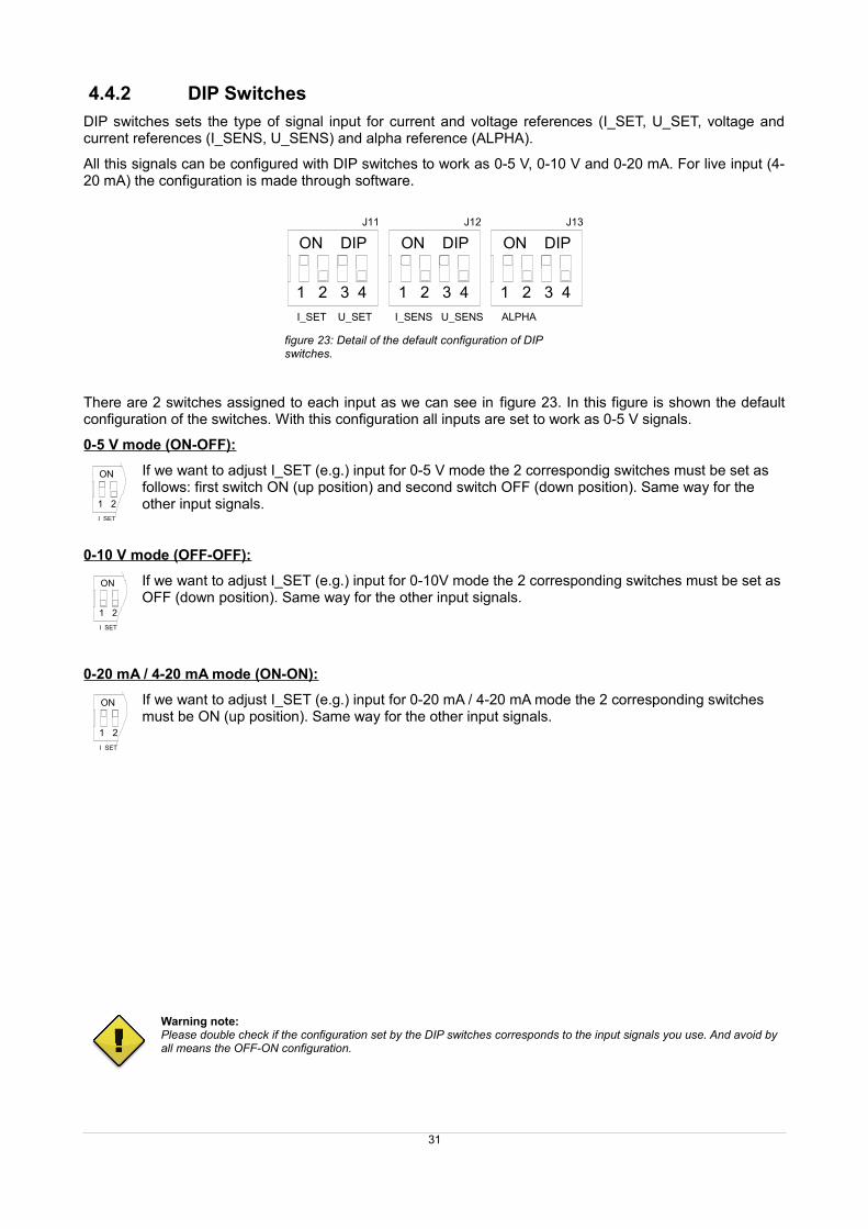
4.4.2 DIP Switches
DIP switches sets the type of signal input for current and voltage references (I_SET, U_SET, voltage andcurrent references (I_SENS, U_SENS) and alpha reference (ALPHA).
All this signals can be configured with DIP switches to work as 0-5 V, 0-10 V and 0-20 mA. For live input (4-20 mA) the configuration is made through software.
There are 2 switches assigned to each input as we can see in figure 23. In this figure is shown the defaultconfiguration of the switches. With this configuration all inputs are set to work as 0-5 V signals.
0-5 V mode (ON-OFF):
If we want to adjust I_SET (e.g.) input for 0-5 V mode the 2 correspondig switches must be set as follows: first switch ON (up position) and second switch OFF (down position). Same way for the other input signals.
0-10 V mode (OFF-OFF):
If we want to adjust I_SET (e.g.) input for 0-10V mode the 2 corresponding switches must be set as OFF (down position). Same way for the other input signals.
0-20 mA / 4-20 mA mode (ON-ON):
If we want to adjust I_SET (e.g.) input for 0-20 mA / 4-20 mA mode the 2 corresponding switches must be ON (up position). Same way for the other input signals.
Warning note: Please double check if the configuration set by the DIP switches corresponds to the input signals you use. And avoid by all means the OFF-ON configuration.
31
figure 23: Detail of the default configuration of DIP switches.
ON DIP
1 2 3 4
ON DIP
1 2 3 4
ON DIP
1 2 3 4
I_SET U_SET I_SENS U_SENS ALPHA
J11 J12 J13
ON
1 2
ON
1 2
ON
1 2
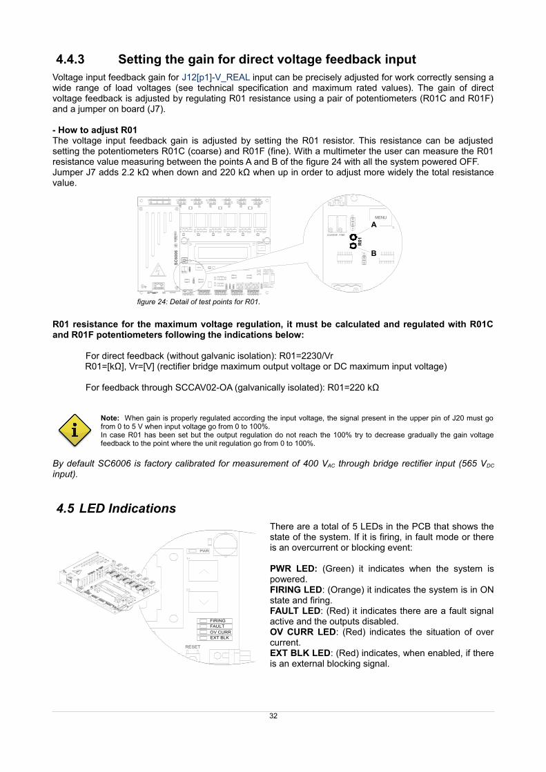
4.4.3 Setting the gain for direct voltage feedback inputVoltage input feedback gain for J12[p1]-V_REAL input can be precisely adjusted for work correctly sensing awide range of load voltages (see technical specification and maximum rated values). The gain of directvoltage feedback is adjusted by regulating R01 resistance using a pair of potentiometers (R01C and R01F)and a jumper on board (J7).
- How to adjust R01The voltage input feedback gain is adjusted by setting the R01 resistor. This resistance can be adjustedsetting the potentiometers R01C (coarse) and R01F (fine). With a multimeter the user can measure the R01resistance value measuring between the points A and B of the figure 24 with all the system powered OFF.Jumper J7 adds 2.2 kΩ when down and 220 kΩ when up in order to adjust more widely the total resistancevalue.
R01 resistance for the maximum voltage regulation, it must be calculated and regulated with R01Cand R01F potentiometers following the indications below:
For direct feedback (without galvanic isolation): R01=2230/VrR01=[kΩ], Vr=[V] (rectifier bridge maximum output voltage or DC maximum input voltage)
For feedback through SCCAV02-OA (galvanically isolated): R01=220 kΩ
Note: When gain is properly regulated according the input voltage, the signal present in the upper pin of J20 must gofrom 0 to 5 V when input voltage go from 0 to 100%. In case R01 has been set but the output regulation do not reach the 100% try to decrease gradually the gain voltagefeedback to the point where the unit regulation go from 0 to 100%.
By default SC6006 is factory calibrated for measurement of 400 VAC through bridge rectifier input (565 VDC
input).
4.5 LED IndicationsThere are a total of 5 LEDs in the PCB that shows thestate of the system. If it is firing, in fault mode or thereis an overcurrent or blocking event:
PWR LED: (Green) it indicates when the system ispowered.FIRING LED: (Orange) it indicates the system is in ONstate and firing.FAULT LED: (Red) it indicates there are a fault signalactive and the outputs disabled.OV CURR LED: (Red) indicates the situation of overcurrent.EXT BLK LED: (Red) indicates, when enabled, if thereis an external blocking signal.
32
PWR
RESET
EXT BLKOV CURR
FAULTFIRING
figure 24: Detail of test points for R01.
MENU
COARSE FINE
R01
A
B
3 8 9 10 11 12 13 14 15 16 17 18 19 20 214 5 6 7 22
N RST
PWR
SC6006
G6 K6K5G5K4G4K3G3K2G2K1G1
MENU
ALP HAU_S E NSI_S E NSU_S E TI _S E TI_SENSU_SENS
LC
D C
ON
TR
AS
T
COARSE FINE
1 2
SC
6006
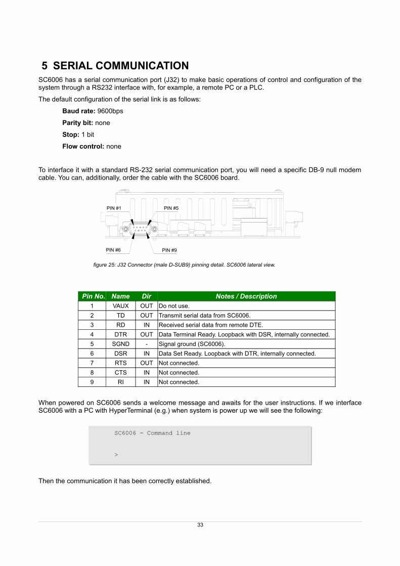
5 SERIAL COMMUNICATIONSC6006 has a serial communication port (J32) to make basic operations of control and configuration of thesystem through a RS232 interface with, for example, a remote PC or a PLC.
The default configuration of the serial link is as follows:
Baud rate: 9600bps
Parity bit: none
Stop: 1 bit
Flow control: none
To interface it with a standard RS-232 serial communication port, you will need a specific DB-9 null modemcable. You can, additionally, order the cable with the SC6006 board.
Pin No. Name Dir Notes / Description
1 VAUX OUT Do not use.
2 TD OUT Transmit serial data from SC6006.
3 RD IN Received serial data from remote DTE.
4 DTR OUT Data Terminal Ready. Loopback with DSR, internally connected.
5 SGND - Signal ground (SC6006).
6 DSR IN Data Set Ready. Loopback with DTR, internally connected.
7 RTS OUT Not connected.
8 CTS IN Not connected.
9 RI IN Not connected.
When powered on SC6006 sends a welcome message and awaits for the user instructions. If we interfaceSC6006 with a PC with HyperTerminal (e.g.) when system is power up we will see the following:
SC6006 - Command line
>
Then the communication it has been correctly established.
33
figure 25: J32 Connector (male D-SUB9) pinning detail. SC6006 lateral view.
PIN #1 PIN #5
PIN #6 PIN #9
5.1 Overview available command setSC6006 has 4 different types of instructions:
– Query instructions (?).
– Signal instructions (*).
– Memory read instructions (R).
– Memory write instructions (S).
To send any instruction to SC6006 and for being processed this instruction must end with a 0x10[“NL”]character (or an enter pulsation if HyperTerminal is used).
All the sent instructions will return back to the user (at least) the 0x10[“NL”] character plus the character ofwaiting for a new instruction: 0x3E[“>”]. This 2 characters will always be sent back even when the echomode is deactivated.
5.2 Query instruction setThe query instructions which starts with 0x3F[“?”] character, gives the user a fast read of usual registers asvoltage feedback register, current feedback register, alpha register, etc. And also get information about thesoftware version installed in the system and its serial number.
5.2.1 “?ver” query version command
Returns the version of the firmware and hardware of the unit.
>?ver
PCB:v1.0 firmware:v1.28
5.2.2 “?S” query status register
Returns the value of the status register. This register is described in chapter 6.1.1 on page 37. Thisinstruction is equivalent to read the register M000.
5.2.3 “?A” query alpha register
Returns the value of the alpha register. This instruction is equivalent to read the register M005.
5.2.4 “?U” query voltage register
Returns the value of the current register. This instruction is equivalent to read the register M008.
5.2.5 “?I” query current register
Returns the value of the status register. This instruction is equivalent to read the register M009.
5.3 Signal instruction setThe signal instructions starts with the 0x2A[“*”] character; this instructions makes a change in the system orsends a signal. Allowing to send a remote push-button signal, remote reset signal, etc. This instructionsreturns no value response but the 0x10[“NL”] and 0x03[“>”] when the instruction has been processed.
34
5.3.1 “*OK” signal command
Sends a remote pulsation of the [OK] push-button.
5.3.2 “*MENU” signal command
Sends a remote pulsation of the [MENU] push-button.
5.3.3 “*UP” signal command
Sends a remote pulsation of the [UP] push-button.
5.3.4 “*DW” signal command
Sends a remote pulsation of the [DW] push-button.
5.3.5 “*RMT” signal command
Enables or disables the remote mode for the SC6006 in order to use it with a remote control LCD asSCRP6006, this command activates a new set of reserved instructions less verbose and more M2Moriented. The description of this additional instruction set is out of the scope of this manual.
5.3.6 “*ECHO” signal command
Enables or disables the echo in serial communication.
When the echoing option is enabled, SC6006 transmits (echoes) data characters it receives back to thesender. When the echoing option is disabled, SC6006 will not echo the characters back to the sender; this,of course, does not prevent SC6006 from responding to data characters received.
This option is intended for a more man-machine friendly interface, for M2M communications disabling echomode reduces the redundant information sent.
Echo mode is, by default, activated.
5.3.7 “*HOME” signal command
Returns the on-board LCD displayed menu to the main menu.
5.3.8 “*RST” signal command
Sends a reset signal to the unit. SC6006 will restart itself.
5.3.9 “*SV” signal command
Sends a save signal to the unit. SC6006 will save all the configuration changes introduced.
35
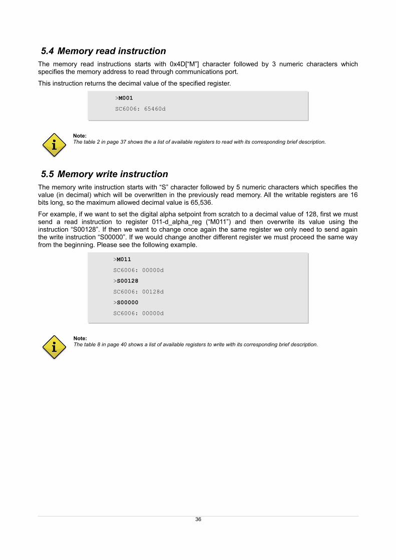
5.4 Memory read instructionThe memory read instructions starts with 0x4D[“M”] character followed by 3 numeric characters whichspecifies the memory address to read through communications port.
This instruction returns the decimal value of the specified register.
>M001
SC6006: 65460d
Note:The table 2 in page 37 shows the a list of available registers to read with its corresponding brief description.
5.5 Memory write instructionThe memory write instruction starts with “S” character followed by 5 numeric characters which specifies thevalue (in decimal) which will be overwritten in the previously read memory. All the writable registers are 16bits long, so the maximum allowed decimal value is 65,536.
For example, if we want to set the digital alpha setpoint from scratch to a decimal value of 128, first we mustsend a read instruction to register 011-d_alpha_reg (“M011”) and then overwrite its value using theinstruction “S00128”. If then we want to change once again the same register we only need to send againthe write instruction “S00000”. If we would change another different register we must proceed the same wayfrom the beginning. Please see the following example.
>M011
SC6006: 00000d
>S00128
SC6006: 00128d
>S00000
SC6006: 00000d
Note: The table 8 in page 40 shows a list of available registers to write with its corresponding brief description.
36
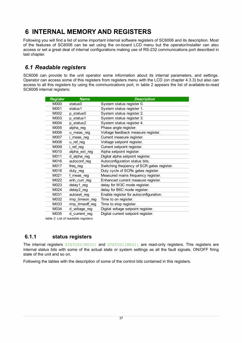
6 INTERNAL MEMORY AND REGISTERSFollowing you will find a list of some important internal software registers of SC6006 and its description. Mostof the features of SC6006 can be set using the on-board LCD menu but the operator/installer can alsoaccess or set a great deal of internal configurations making use of RS-232 communications port described inlast chapter.
6.1 Readable registersSC6006 can provide to the unit operator some information about its internal parameters, and settings.Operator can access some of this registers from registers menu with the LCD (on chapter 4.3.3) but also canaccess to all this registers by using the communications port, in table 2 appears the list of available-to-readSC6006 internal registers:
6.1.1 status registers
The internal registers STATUS0[M000] and STATUS1[M001] are read-only registers. This registers areinternal status bits with some of the actual state or system settings as all the fault signals, ON/OFF firingstate of the unit and so on.
Following the tables with the description of some of the control bits contained in this registers.
37
table 2: List of readable registers.
Register Name DescriptionM000 status0 System status register 0.M001 status1 System status register 1.M002 p_status0 System status register 2.M003 p_status1 System status register 3.M004 p_status2 System status register 4.M005 alpha_reg Phase angle register.M006 u_meas_reg Voltage feedback measure register.M007 i_meas_reg Current measure register.M008 u_ref_reg Voltage setpoint register.M009 i_ref_reg Current setpoint register.M010 alpha_ext_reg Alpha setpoint register.M011 d_alpha_reg Digital alpha setpoint register.M016 autoconf_reg Autoconfiguration status bits.M017 freq_reg Switching freqüency of SCR gates register.M018 duty_reg Duty cycle of SCRs gates register.M021 f_meas_reg Measured mains frequency register.M022 enh_curr_reg Enhanced current measure register.M023 delay1_reg delay for W3C mode register.M024 delay2_reg delay for B6C mode register.M031 autoset_reg Enable register for autoconfiguration.M032 rmp_timeon_reg Time to on register.M033 rmp_timeoff_reg Time to stop register.M034 d_voltage_reg Digital voltage setpoint register.M035 d_current_reg Digital current setpoint register.
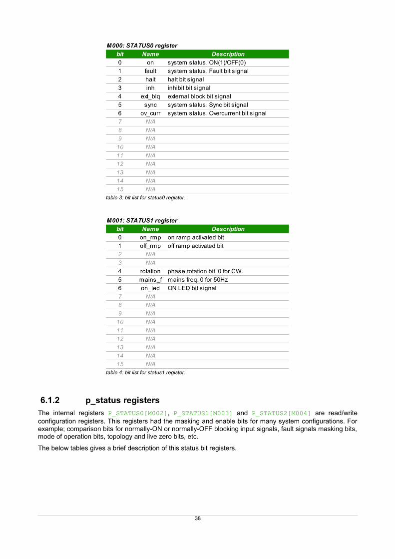
6.1.2 p_status registers
The internal registers P_STATUS0[M002], P_STATUS1[M003] and P_STATUS2[M004] are read/writeconfiguration registers. This registers had the masking and enable bits for many system configurations. Forexample; comparison bits for normally-ON or normally-OFF blocking input signals, fault signals masking bits,mode of operation bits, topology and live zero bits, etc.
The below tables gives a brief description of this status bit registers.
38
table 3: bit list for status0 register.
M000: STATUS0 register
bit Name Description
0 on system status. ON(1)/OFF(0)
1 fault system status. Fault bit signal
2 halt halt bit signal
3 inh inhibit bit signal
4 ext_blq external block bit signal
5 sync system status. Sync bit signal
6 ov_curr system status. Overcurrent bit signal
7 N/A
8 N/A
9 N/A
10 N/A
11 N/A
12 N/A
13 N/A
14 N/A
15 N/A
table 4: bit list for status1 register.
M001: STATUS1 register
bit Name Description
0 on_rmp on ramp activated bit
1 off_rmp off ramp activated bit
2 N/A
3 N/A
4 rotation phase rotation bit. 0 for CW.
5 mains_f mains freq. 0 for 50Hz
6 on_led ON LED bit signal
7 N/A
8 N/A
9 N/A
10 N/A
11 N/A
12 N/A
13 N/A
14 N/A
15 N/A

39
table 5: bit list for p_status0 register.
M002: P_STATUS0 register
bit Name Description
0 en_on enable ON (firing) mode
1 en_fault enable fault signal
2 en_halt enable halt signal
3 en_inh enable inhibit signal
4 en_ext_blq enable external block signal
5 en_sync enable sync fault signal
6 en_ovcurr enable overcurrent fault signal
7 sw_fault enable interlock fault
8 N/A
9 N/A
10 topo0 topology bit. B6C=0, W3C=1
11 N/A
12 N/A
13 backlight enable LCD backlight
14 N/A
15 N/A
table 6: bit list for p_status1 register.
M003: P_STATUS1 register
bit Name Description
0 en_on_rmp enable soft on bit
1 en_of f_rmp enable soft off bit
2 en_auto_pw ron enable startup bit
3 en_last_state enable last state start up bit
4 N/A
5 u_meas_lz voltage feedback live zero
6 i_meas_lz current feedback live zero
7 u_ref_lz voltage setpoint live zero
8 i_ref_lz current setpoint live zero
9 alpha_lz alpha setpoint live zero
10 N/A
11 N/A
12 N/A
13 N/A
14 N/A
15 N/A

Warning note: Take special care when attempting to change any of the configuration bits of p_status registers, if accidentally a wrong value is written the system can stop working or malfunction.
6.2 Writable registersIn table 8 appears the list of available-to-write SC6006 internal settings registers and its brief description. It isalso specified the valid value range (decimal integer) for each register.
Warning note: Please do not attempt to make a writing in a register not appearing in table 8.And do not write to a register a value out ofthe defined range.
40
table 7: bit list for p_status2 register.
M004: P_STATUS2 register
bit Name Description
0 u_ref_src voltage setpoint reference bit
1 i_ref_src current setpoint reference bit
2 N/A
3 N/A
4 alpha_ref_src alpha setpoint reference bit
5 N/A
6 N/A
7 echo comm. echo mode
8 mode0 mode0 bit. PSA=0 FWS=1
9 mode1 mode1 bit. RLY=1
10 N/A
11 N/A
12 fb0 feedback mode bits:
13 fb1 00:I, 01:V, 10:IV, 11:OL
14 N/A
15 N/A
table 8: list of writable registers.
Register Name Description Range
M002 p_status0 System status register 2. N/A
M003 p_status1 System status register 3. N/A
M004 p_status2 System status register 4. N/A
M011 d_alpha_reg Digital alpha setpoint register. [0..1023]
M017 f req_reg Switching freqüency of SCR gates register. [10..20]
M018 duty_reg Duty cycle of SCRs gates register. [10..30]
M023 delay1_reg delay for W3C mode register. [0..400]
M024 delay2_reg delay for B6C mode register. [0..400]
M032 rmp_timeon_reg Time to on register. [1..30]
M033 rmp_timeoff_reg Time to stop register. [1..30]
M034 d_voltage_reg Digital voltage setpoint register. [0..1023]
M035 d_current_reg Digital current setpoint register. [0..1023]
M036 ov_current_reg Maximum overcurrent reference. [50..300]
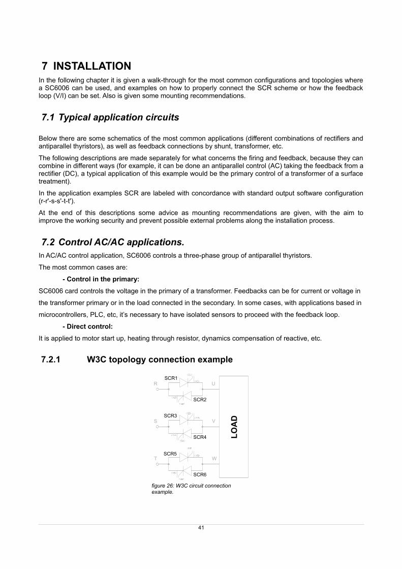
7 INSTALLATIONIn the following chapter it is given a walk-through for the most common configurations and topologies wherea SC6006 can be used, and examples on how to properly connect the SCR scheme or how the feedbackloop (V/I) can be set. Also is given some mounting recommendations.
7.1 Typical application circuits
Below there are some schematics of the most common applications (different combinations of rectifiers andantiparallel thyristors), as well as feedback connections by shunt, transformer, etc.
The following descriptions are made separately for what concerns the firing and feedback, because they cancombine in different ways (for example, it can be done an antiparallel control (AC) taking the feedback from arectifier (DC), a typical application of this example would be the primary control of a transformer of a surfacetreatment).
In the application examples SCR are labeled with concordance with standard output software configuration(r-r'-s-s'-t-t').
At the end of this descriptions some advice as mounting recommendations are given, with the aim toimprove the working security and prevent possible external problems along the installation process.
7.2 Control AC/AC applications.In AC/AC control application, SC6006 controls a three-phase group of antiparallel thyristors.
The most common cases are:
- Control in the primary:
SC6006 card controls the voltage in the primary of a transformer. Feedbacks can be for current or voltage in
the transformer primary or in the load connected in the secondary. In some cases, with applications based in
microcontrollers, PLC, etc, it’s necessary to have isolated sensors to proceed with the feedback loop.
- Direct control:
It is applied to motor start up, heating through resistor, dynamics compensation of reactive, etc.
7.2.1 W3C topology connection example
41
figure 26: W3C circuit connection example.
SCR1
SCR2
SCR4
SCR3
SCR6
SCR5
LO
AD
R
S
T
U
V
W
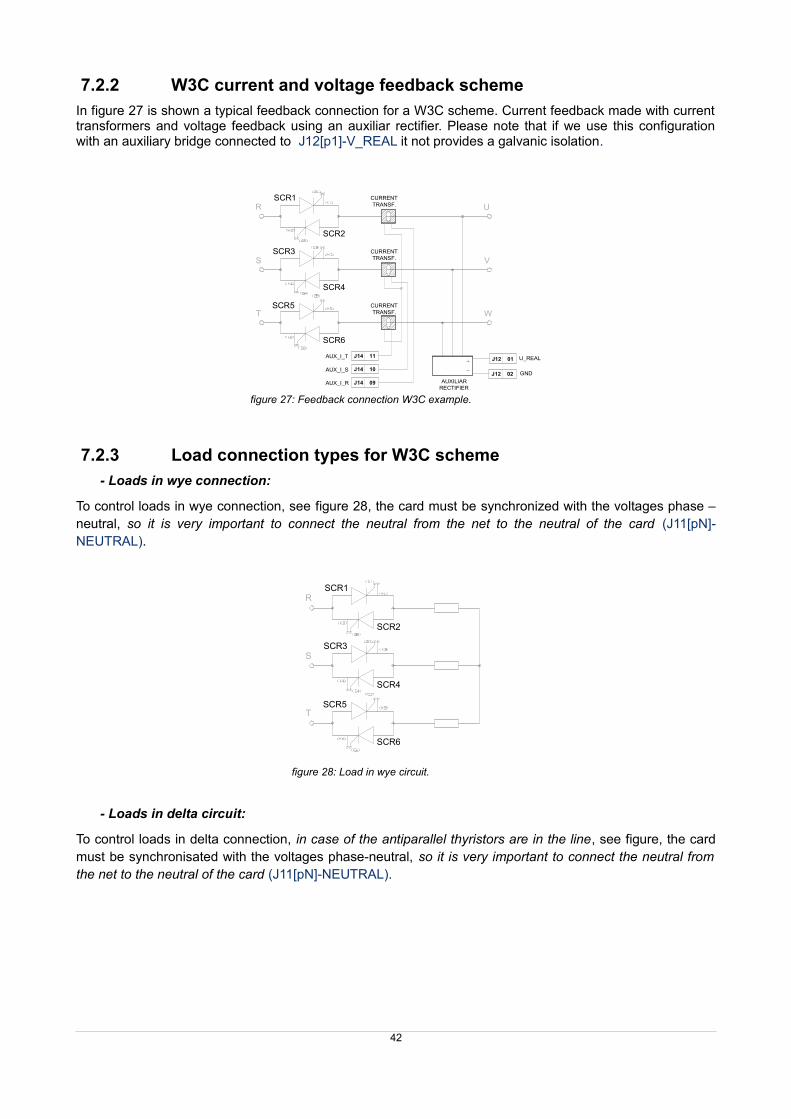
7.2.2 W3C current and voltage feedback scheme
In figure 27 is shown a typical feedback connection for a W3C scheme. Current feedback made with currenttransformers and voltage feedback using an auxiliar rectifier. Please note that if we use this configurationwith an auxiliary bridge connected to J12[p1]-V_REAL it not provides a galvanic isolation.
7.2.3 Load connection types for W3C scheme
- Loads in wye connection:
To control loads in wye connection, see figure 28, the card must be synchronized with the voltages phase –neutral, so it is very important to connect the neutral from the net to the neutral of the card (J11[pN]-NEUTRAL).
- Loads in delta circuit:
To control loads in delta connection, in case of the antiparallel thyristors are in the line, see figure, the cardmust be synchronisated with the voltages phase-neutral, so it is very important to connect the neutral fromthe net to the neutral of the card (J11[pN]-NEUTRAL).
42
figure 27: Feedback connection W3C example.
figure 28: Load in wye circuit.
SCR1
SCR2
SCR4
SCR3
SCR6
SCR5
R
S
TCURRENTTRANSF.
J14 09AUX_I_R
J14 10AUX_I_S
J14 11AUX_I_T
CURRENTTRANSF.
CURRENTTRANSF. U
V
W
J12 01 U_REAL
J12 02 GND
AUXILIARRECTIFIER
SCR1
SCR2
SCR4
SCR3
SCR6
SCR5
R
S
T
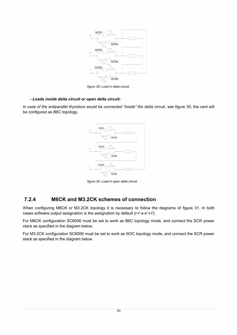
- Loads inside delta circuit or open delta circuit:
In case of the antiparallel thyristors would be connected “inside” the delta circuit, see figure 30, the card willbe configured as B6C topology.
7.2.4 M6CK and M3.2CK schemes of connection
When configuring M6CK or M3.2CK topology it is necessary to follow the diagrams of figure 31. In bothcases software output assignation is the assignation by default (r-r'-s-s'-t-t').
For M6CK configuration SC6006 must be set to work as B6C topology mode, and connect the SCR powerstack as specified in the diagram below.
For M3.2CK configuration SC6006 must be set to work as W3C topology mode, and connect the SCR powerstack as specified in the diagram below.
43
figure 29: Load in delta circuit.
figure 30: Load in open delta circuit.
SCR1
SCR2
SCR4
SCR3
SCR6
SCR5
R
S
T
SCR1
SCR2
SCR4
SCR3
SCR6
SCR5
R
S
T

Note: Autoset function will not be capable to determine the output connection for this topologies due its common cathodeconnection. The user must check the concordance between the software output phase assignation and the wiring to theSCRs.
7.3 Control AC/DC applications. B6C scheme.In AC/DC control application, SC6006 controls a three-phase thyristors bridge. They have a wide range ofapplications from electro-chemical processes, traction equipment, controlled power supplies, etc.
7.3.1 B6C topology connection example
7.3.2 DC current sense feedback using a shunt
If a shunt is used to sense the output current in a AC/DC topology then it must be checked, or decided, if theshunt is placed on the positive ouptut terminal or on the negative one. Then the controller board should beconfigured according this configuration and wired (the connections for current and voltage feedback signals)following the next specifications.
- Shunt on positive terminal
When a shunt is used on the positive output terminal and the voltage feedback measure is done with directvoltage input feedback J12[p1]-V_REAL, shunt negative reference must be connected to J14[p8]-GND andits positive sensing terminal to J14[p12]-I_SHUNT. Jumper JP23 must be set in UP position as specified inchapter 4.4.1 on page 30. So, if a current measure through shunt and a direct voltage measurement is done,voltage and current measures must be connected as is shown in figure 33.
44
figure 32: B6C topology connection example.
figure 31: M6CK and M3.2CK connection schemes.
R
ST
R
ST
M6CK connection scheme M3.2CK connection scheme
SCR2
LO
AD
+
-
R
S
T
SCR1 SCR3 SCR5
SCR6SCR4
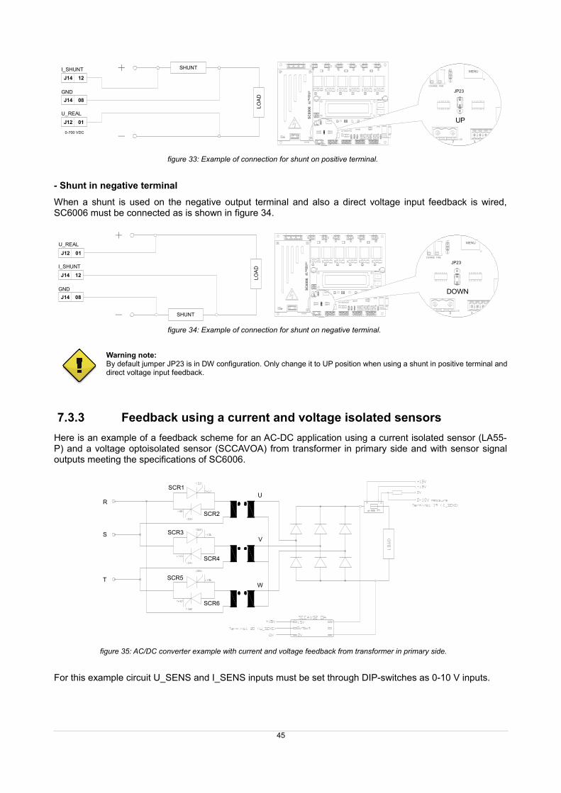
- Shunt in negative terminal
When a shunt is used on the negative output terminal and also a direct voltage input feedback is wired,SC6006 must be connected as is shown in figure 34.
Warning note:By default jumper JP23 is in DW configuration. Only change it to UP position when using a shunt in positive terminal anddirect voltage input feedback.
7.3.3 Feedback using a current and voltage isolated sensors
Here is an example of a feedback scheme for an AC-DC application using a current isolated sensor (LA55-P) and a voltage optoisolated sensor (SCCAVOA) from transformer in primary side and with sensor signaloutputs meeting the specifications of SC6006.
For this example circuit U_SENS and I_SENS inputs must be set through DIP-switches as 0-10 V inputs.
45
figure 33: Example of connection for shunt on positive terminal.
figure 34: Example of connection for shunt on negative terminal.
figure 35: AC/DC converter example with current and voltage feedback from transformer in primary side.
S
R
T
SCR1
SCR2
SCR4
SCR3
SCR6
SCR5
V
U
W
J14 12
I_SHUNT
J14 08
J12 01
U_REAL
0-700 VDC
SHUNT
LO
AD
GND
8 9 10 11 12 13 14 15 16 17 18 19 20 214 5 6 7 22
N RST
PWR
SC6006
G6 K6K5G5K4G4K3G3K2G2K1G1
MENU
ALPHAU_SENSI_SENSU_SETI_SETI_SENSU_SENS
LCD
CO
NTR
AS
T
COARSE FINE
1 2
SC
6006
3
MENU
COARSE FINE
2
JP23
UP
8 9 10 11 12 13 14 15 16 17 18 19 20 214 5 6 7 22
N RST
PWR
SC6006
G6 K6K5G5K4G4K3G3K2G2K1G1
MENU
ALPHAU_SENSI_SENSU_SETI_SETI_SENSU_SENS
LCD
CO
NT
RA
ST
COARSE FINE
1 2
SC
600
6
3
MENU
COARSE FINE
2
JP23
DOWN
J14 12
I_SHUNT
J14 08
J12 01
U_REAL
SHUNT
LO
AD
GND
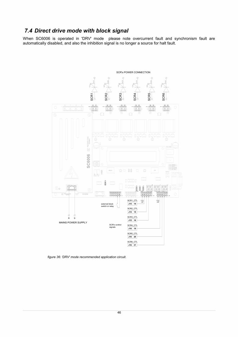
7.4 Direct drive mode with block signalWhen SC6006 is operated in 'DRV' mode please note overcurrent fault and synchronism fault areautomatically disabled, and also the inhibition signal is no longer a source for halt fault.
46
figure 36: 'DRV' mode recommended application circuit.
3 8 9 10 11 12 13 14 15 16 17 18 19 20 214 5 6 7 22
N RST
PWR
RESET
EXT BLKOV CURR
FAULTFIRING
SC6006
G6 K6K5G5K4G4K3G3K2G2K1G1
MENU OK
ALPHAU_SENSI_SENSU_SETI_SETI_SENSU_SENS
LC
D C
ON
TR
AS
T
COARSE FINE
1 2
SC
600
6
J15 14
SCR1_CTL
J15 15
J15 16
J16 19
J16 20
J16 21
SCR2_CTL
SCR3_CTL
SCR4_CTL
SCR5_CTL
SCR6_CTL
SC
R1
SC
R2
SC
R3
SC
R4
SC
R5
SC
R6
external blockswitch or relay
COMGND
COMGND
MAINS POWER SUPPLY
R S
SCR's controlsignals
SCR's POWER CONNECTION
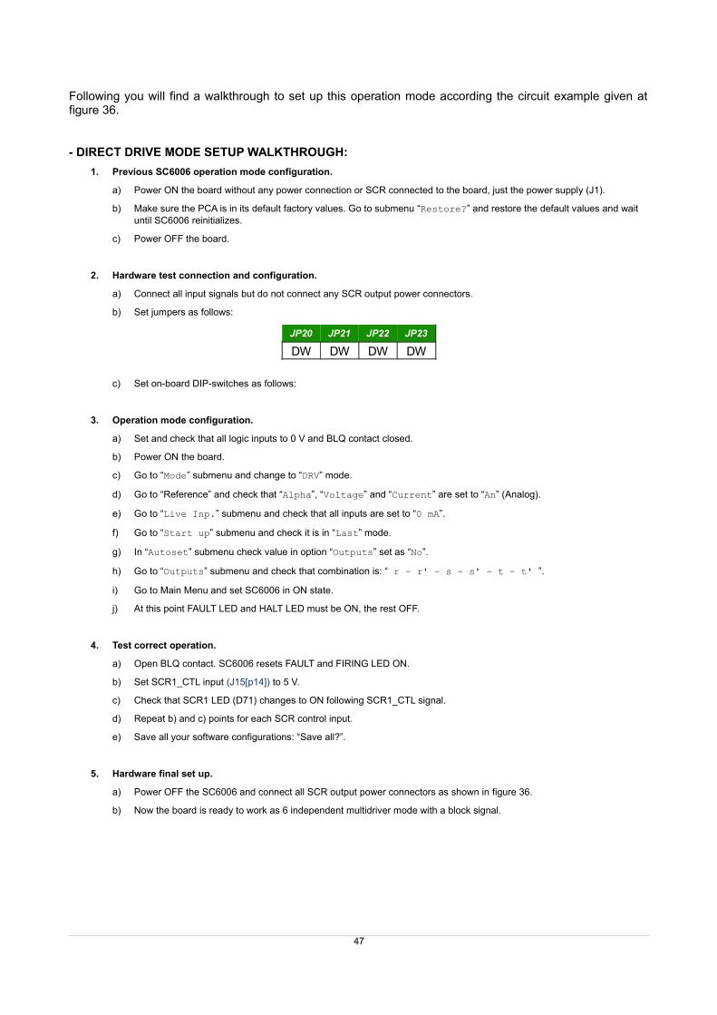
Following you will find a walkthrough to set up this operation mode according the circuit example given atfigure 36.
- DIRECT DRIVE MODE SETUP WALKTHROUGH:
1. Previous SC6006 operation mode configuration.
a) Power ON the board without any power connection or SCR connected to the board, just the power supply (J1).
b) Make sure the PCA is in its default factory values. Go to submenu “Restore?” and restore the default values and wait until SC6006 reinitializes.
c) Power OFF the board.
2. Hardware test connection and configuration.
a) Connect all input signals but do not connect any SCR output power connectors.
b) Set jumpers as follows:
JP20 JP21 JP22 JP23
DW DW DW DW
c) Set on-board DIP-switches as follows:
3. Operation mode configuration.
a) Set and check that all logic inputs to 0 V and BLQ contact closed.
b) Power ON the board.
c) Go to “Mode” submenu and change to “DRV” mode.
d) Go to “Reference” and check that “Alpha”, “Voltage” and “Current” are set to “An” (Analog).
e) Go to “Live Inp.” submenu and check that all inputs are set to “0 mA”.
f) Go to “Start up” submenu and check it is in “Last” mode.
g) In “Autoset” submenu check value in option “Outputs” set as “No”.
h) Go to “Outputs” submenu and check that combination is: “ r – r' – s – s' – t – t' ”.
i) Go to Main Menu and set SC6006 in ON state.
j) At this point FAULT LED and HALT LED must be ON, the rest OFF.
4. Test correct operation.
a) Open BLQ contact. SC6006 resets FAULT and FIRING LED ON.
b) Set SCR1_CTL input (J15[p14]) to 5 V.
c) Check that SCR1 LED (D71) changes to ON following SCR1_CTL signal.
d) Repeat b) and c) points for each SCR control input.
e) Save all your software configurations: “Save all?”.
5. Hardware final set up.
a) Power OFF the SC6006 and connect all SCR output power connectors as shown in figure 36.
b) Now the board is ready to work as 6 independent multidriver mode with a block signal.
47
7.5 Mounting recommendations
7.5.1 General mounting recommendations
1- Avoid long cables in the firing system, or use twisted or shielded cables. Apply it also for thepotentiometer cables.
2- Ground the device in accordance with local regulations.
3- Make sure that the board is not in environments of strong magnetic fields, for example, high powertransformers, or apply it a conductive envelop connected to ground.
3- For use it in inductive or capacitive loads, with regular connection cycles, it’s recommended to use afixed resistive load (with low value), in order to avoid any kind of error during the start up process(this is valid for all assemblies).
4- Is convenient to realize working tests with small loads (for example, bulbs or resistors), in this way ifthere is any connection error will be detected without further consequences. It’s important to knowthat the feedback susceptibility couldn’t be enough with loads which consumes very low current,thus, the control operation can be wrong.
5- In AC current control applications with voltage regulation, it must be added the auxiliary rectifiermodule SCCAV02, knowing that the galvanic isolation disappears with the net, otherwise use theisolated version SCCAV02 OA.
6- Shunt elements doesn’t provide galvanic isolation in current feedback power stage. If galvanicisolation is a requirement, it must be used isolated current sensors (Hall sensors).
7- In applications with presence of variable loads, parasitic in the net, regulations with minimums voltageand currents, can cause non desired oscillation regulations. For this cases, please contact to ourtechnical department.
8- Install the device in a upright or flat position and ensure a minimum ventilation distance betweensurroundings. If mounted in a cabinet ensure sufficient ventilation and always observe minimumspacing (clearance: 150 mm above and below).
8- For specific applications, there is the possibility to realize customized software and hardwareadaptations and include auxiliary control modules, so please, don’t hesitate to ask about yourapplication.
7.5.2 Recommended start up procedure
CAUTION:Before plugging the supply voltage for the control unit, be sure that the card is locked or will be start up in OFF mode and set the regulation potentiometers to the minimum level.
1- Lock the card through external blocking switch.
2- Regulate to the minimum level all the voltage and current or alpha potentiometers or setpoints.
3- If Autoset mode is configured for check and set the mains frequency operation, the phase rotation oroutputs assignation, it will be done when the control board is powered up. Then SC6006 must bepowered after or at the same time as the power stack.
48

4- Check operation and configuration settings are correct for your application.
7.5.3 Notes about the control card in systems controlled by microcontrollers or PLC
In those cases SC6006 is controlled by a external system, microcontroller, PLC, etc, it’s essential to guarantygalvanic isolation between control signals and power circuits. The lack of isolation may cause a currentcirculation between the power stage and the power control circuits, thus, most cases the control elementsget damaged.
The personal in charge of the design of this system should be qualified enough to manage isolation tests.
In case of doubt, please contact to our technical department where we can look for the best option.
49

8 AVAILABLE ACCESSORIES
There are available several accessories to work with the SC6006 which will be briefly described in thissection, those accessories are normally used in applications with the firing board to enhance or complete itsintegration in a power converter.
8.1 SCRP6006SCRP6006 (datasheet) is specially designed to interface our SC6006 SCR digital firing board. It provides aneat and easy way to remotely monitor and set up SC6006 SCR controller board using its serial interface.This panel expands the on-board LCD screen, buttons and status LEDs for mounting in a cabinet door.Additionally provides an extension to SC6006 serial link communication port.
Typical application
8.1.1 Interfacing SC6006 with remote panel SCRP6006.
To use a remote panel interfacing SC6006 for a door cabinet e.g. on figure 37 is shown how to connect itwith SC6006. An standard DB-9 cable M to F is needed and on SC6006 the jumper 24 must be set on downposition and configure, through LCD on board, the communication with the remote panel.
SUBMENU 1.9: COM > Remote > [En / Dis]
50
figure 37: Example of connection between SC6006 and SCRP6006.
SCRP6006 BACKSIDE
J24 - SCRP6006 COMJUMPER
Standard Male-Female DB-9 Cable.(Provided with SCRP6006)
SCRP6006 FRONTSIDE
SE
MIC
OD
EE
LE
CT
RO
NIC
A
®
SC
60
06
3 8 9 10 11 12 13 14 15 16 17 18 19 20 214 5 6 7 22
N RST
PWR
RESET
EXT BLKOV CURRFAULTFIRING
SC6006
G6 K6K5G5K4G4K3G3K2G2K1G1
MENU OK
ALPHAU_SENSI_SENSU_SETI_SETI_SENSU_SENS
LCD
CO
NT
RA
ST
COARSE FINE
1 2
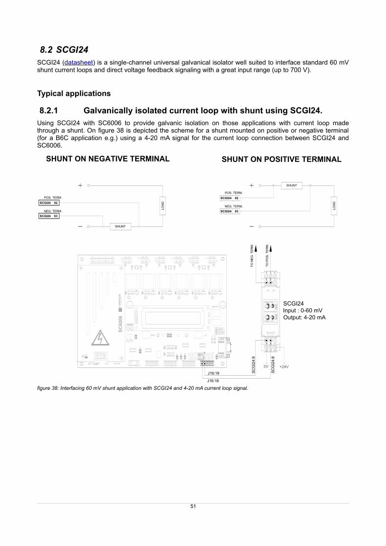
8.2 SCGI24SCGI24 (datasheet) is a single-channel universal galvanical isolator well suited to interface standard 60 mVshunt current loops and direct voltage feedback signaling with a great input range (up to 700 V).
Typical applications
8.2.1 Galvanically isolated current loop with shunt using SCGI24.
Using SCGI24 with SC6006 to provide galvanic isolation on those applications with current loop madethrough a shunt. On figure 38 is depicted the scheme for a shunt mounted on positive or negative terminal(for a B6C application e.g.) using a 4-20 mA signal for the current loop connection between SCGI24 andSC6006.
51
figure 38: Interfacing 60 mV shunt application with SCGI24 and 4-20 mA current loop signal.
SE
MIC
OD
EE
LE
CT
RO
NIC
A
®
SC
6006
SHUNT
LOA
D
SHUNT ON POSITIVE TERMINALSHUNT ON NEGATIVE TERMINAL
POS. TERM.
SHUNT
NEG. TERM.
SCGI24 02
POS. TERM.
NEG. TERM.
LOA
D
SCGI24Input : 0-60 mVOutput: 4-20 mA
J16:19
J16:18
SC
GI2
4:8
SC
GI2
4:9
TO
PO
S. T
ER
M.
TO
NE
G. T
ER
M.
SCGI24 03
SCGI24 02
SCGI24 03
0V +24V
123
456
789
101112
GRUESO FINO CE
RO
SP
AN
GRUESO FINO
3 8 9 10 11 12 13 14 15 16 17 18 19 20 214 5 6 7 22
N RST
PWR
RESET
EXT BLKOV CURR
FAULTFIRING
SC6006
G6 K6K5G5K4G4K3G3K2G2K1G1
MENU OK
ALPHAU_SENSI_SENSU_SETI_SETI_SENSU_SENS
LCD
CO
NT
RA
ST
COARSE FINE
1 2
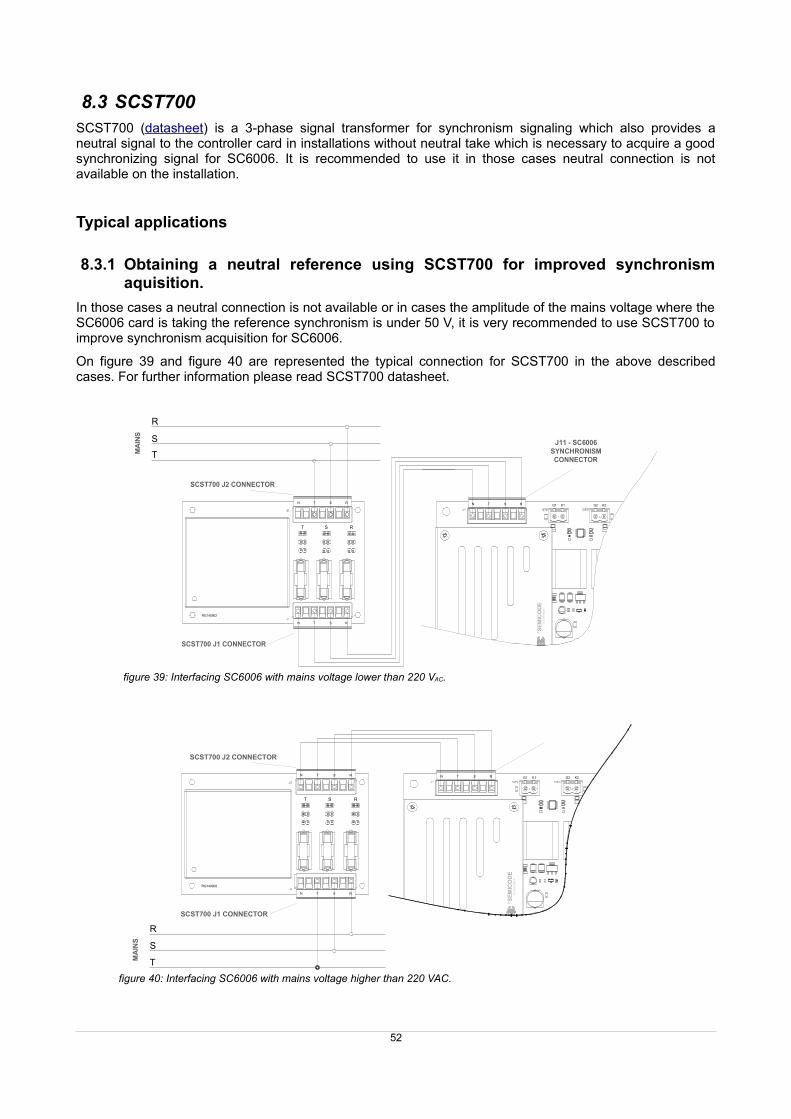
8.3 SCST700SCST700 (datasheet) is a 3-phase signal transformer for synchronism signaling which also provides aneutral signal to the controller card in installations without neutral take which is necessary to acquire a goodsynchronizing signal for SC6006. It is recommended to use it in those cases neutral connection is notavailable on the installation.
Typical applications
8.3.1 Obtaining a neutral reference using SCST700 for improved synchronismaquisition.
In those cases a neutral connection is not available or in cases the amplitude of the mains voltage where theSC6006 card is taking the reference synchronism is under 50 V, it is very recommended to use SCST700 toimprove synchronism acquisition for SC6006.
On figure 39 and figure 40 are represented the typical connection for SCST700 in the above describedcases. For further information please read SCST700 datasheet.
52
figure 39: Interfacing SC6006 with mains voltage lower than 220 VAC.
K2G2K1G1
J11 - SC6006SYNCHRONISMCONNECTOR
SE
MIC
OD
EE
LEC
TR
ON
ICA
®
N RST
N RST
RG140902
T S R
N RST
S
T
R
SCST700 J2 CONNECTOR
SCST700 J1 CONNECTOR
MA
INS
figure 40: Interfacing SC6006 with mains voltage higher than 220 VAC.
K2G2K1G1
SE
MIC
OD
EE
LE
CT
RO
NIC
A
®
N RST
N RST
RG140902
T S R
N RST
S
T
R
SCST700 J2 CONNECTOR
SCST700 J1 CONNECTOR
MA
INS
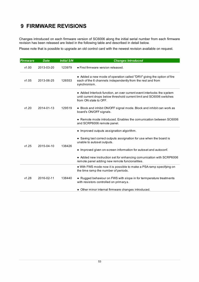
9 FIRMWARE REVISIONS
Changes introduced on each firmware version of SC6006 along the initial serial number from each firmwarerevision has been released are listed in the following table and described in detail below.
Please note that is possible to upgrade an old control card with the newest revision available on request.
53
Firmware Date Initial S/N Changes Introduced
v1.00 2013-03-20 123979
v1.05 2013-06-25 126553
v1.20 2014-01-13 129519
v1.25 2015-04-10 138426
v1.28 2016-02-11 138440
First firmware version released.
Added a new mode of operation called "DRV" giving the option of fire each of the 6 channels independently from the rest and from synchronism.
Added Interlock function, an over current event interlocks the system until current drops below threshold current limit and SC6006 switches from ON state to OFF.
Block and inhibit ON/OFF signal mode. Block and inhibit can work as board's ON/OFF signals.
Remote mode introduced. Enables the comunication between SC6006 and SCRP6006 remote panel.
Improved outputs assignation algorithm.
Saving last correct outputs assignation for use when the board is unable to autoset outputs.
Improved given on-screen information for autoset and autoconf.
Added new instruction set for enhancing comunication with SCRP6006 remote panel adding new remote funcionalities.
With FWS mode now it is possible to make a PSA ramp specifying on the time ramp the number of periods.
Rugged behaviour on FWS with slope in for termperature treatments with resistors controlled on primary.s.
Other minor internal firmware changes introduced.
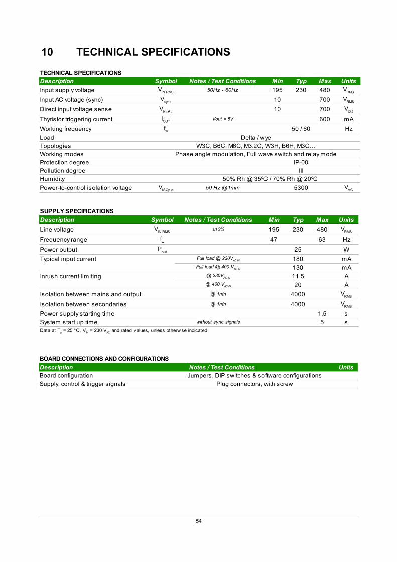
10 TECHNICAL SPECIFICATIONS
54
TECHNICAL SPECIFICATIONS
Description Symbol Notes / Test Conditions Min Typ Max Units
Input supply voltage 50Hz - 60Hz 195 230 480
Input AC voltage (sync) 10 700
Direct input voltage sense 10 700
Thyristor triggering current Vout = 5V 600 mA
Working frequency 50 / 60 Hz
Load Delta / wye
Topologies W3C, B6C, M6C, M3.2C, W3H, B6H, M3C…
Working modes
Protection degree IP-00
Pollution degree III
Humidity 50% Rh @ 35ºC / 70% Rh @ 20ºC
Power-to-control isolation voltage 50 Hz @1min 5300
VIN RMS
VRMS
Vsync
VRMS
VREAL VDC
IOUT
fw
Phase angle modulation, Full wave switch and relay mode
VISOp-c
VAC
SUPPLY SPECIFICATIONS
Description Symbol Notes / Test Conditions Min Typ Max Units
Line voltage 195 230 480
Frequency range 47 63 Hz
Power output 25 W
Typical input current 180 mA
130 mA
Inrush current limiting 11,5 A
20 A
Isolation between mains and output @ 1min 4000
Isolation between secondaries @ 1min 4000
Power supply starting time 1.5 s
System start up time without sync signals 5 s
VIN RMS
±10% VRMS
fw
Pout
Full load @ 230VAC IN
Full load @ 400 VAC IN
@ 230VAC IN
@ 400 VAC IN
VRMS
VRMS
Data at Ta = 25 °C, V
IN = 230 V
AC and rated v alues, unless otherwise indicated
BOARD CONNECTIONS AND CONFIGURATIONS
Description Notes / Test Conditions UnitsBoard configuration Jumpers, DIP switches & software configurations
Supply, control & trigger signals Plug connectors, with screw

BLOCK DIAGRAM
55
INPUT REFERENCE AND FEEDBACK SIGNALS
Description Symbol Notes / Test Conditions Min Typ Max Units
Voltage setpoint 0 20 mA
Current setpoint 4 20 mA
Alpha setpoint 0 10 V
Voltage feedback signal 0 5 V
Voltage direct feedback 10 700
0 200 mA
Current feedback (from shunt.) 0 60 mV
External lock NO/NC software configurable External relay
Inhibit NO/NC software configurable 5 V
Output fault dry relay current 1.5 A
Output fault dry relay voltage 250
[1] Current inputs allows a peak input 3 times the maximum nominal current sensing.
VIN ref
depending of the on board DIP-switches conf iguration and sof tware
settings.
IIN ref
αIN ref
VIN fb
Current feedback signal [1] IIN fb
VIN dfb
Vpeak
Current feedback (from curr. Trans.) [1] IIN trf
IIN shunt
IK2
VK2
VRMS
Setpoints & reference inputs
C.T. feedback input
Shunt feedback input
Direct voltage feedback input
3
SCR drivers
Block
Inhibit
Fault
Setpoints3
2
References
Synch
Fault
Ext. Block
Alpha, current&
voltage
GND
ToCOM
Device
Vcc
Vdd
From mainscurrent
transformers
Fromshunt
Fromload
Pulse transformers
SCR FIRING BOARD
Neutral
ToSCRs
5
2
OV. CURR.DETECTOR
2
7
DSPb
RS232Serial
Interface LCD Display 20x2 char.
Line IN
PULSETRAIN
SHAPINGCIRCUIT
Cathode synch. detector
R, S, T IN
SMPS Power Supply
3
4
Digital I/O
6
DSPa
Synch block
EMIFILTER
RECTIFIERS&
FILTER
POWERSWITCHING
PWMCONTROL
RECTIFIERS&
FILTERS
DETECTIONCIRCUIT
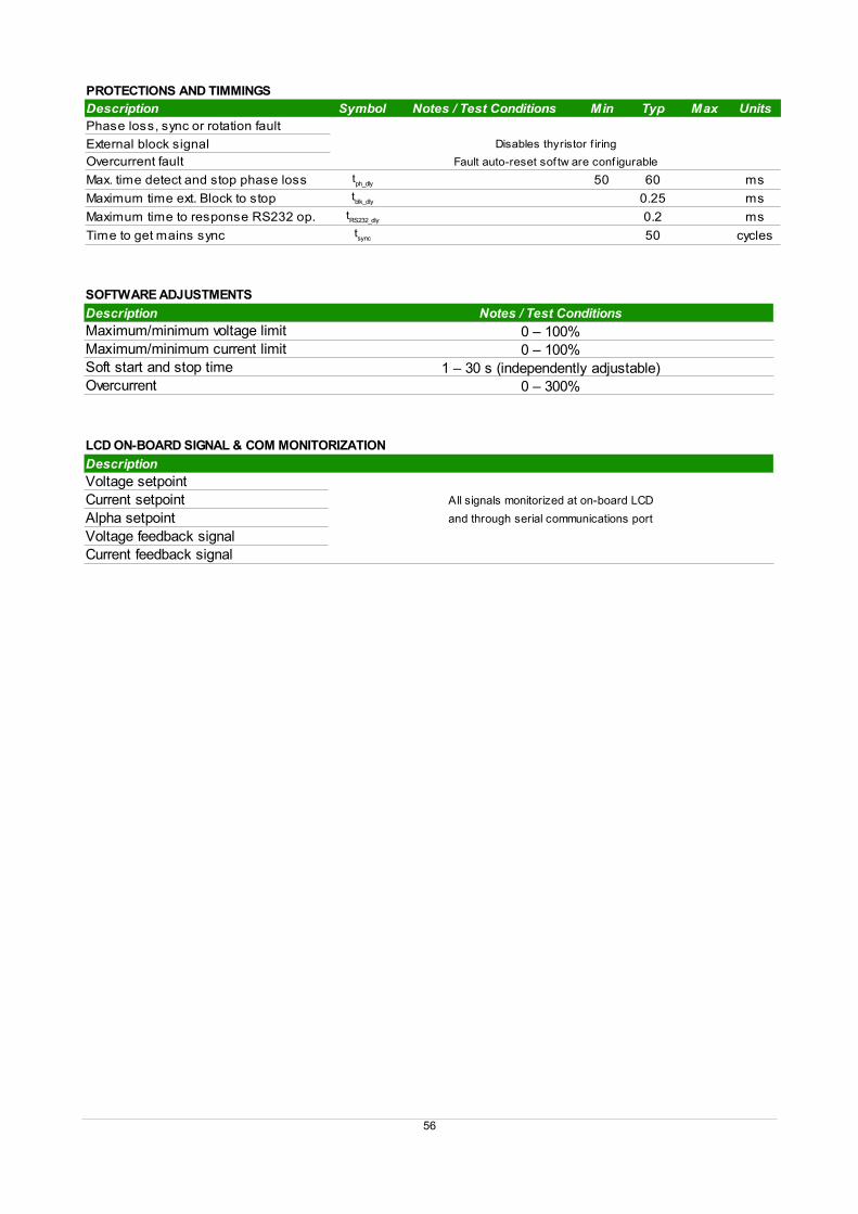
56
PROTECTIONS AND TIMMINGS
Description Symbol Notes / Test Conditions Min Typ Max UnitsPhase loss, sync or rotation fault
External block signal Disables thyristor f iring
Overcurrent fault Fault auto-reset sof tw are conf igurable
Max. time detect and stop phase loss 50 60 ms
Maximum time ext. Block to stop 0.25 ms
Maximum time to response RS232 op. 0.2 ms
Time to get mains sync 50 cycles
tph_dly
tblk_dly
tRS232_dly
tsync
SOFTWARE ADJUSTMENTS
Description Notes / Test ConditionsMaximum/minimum voltage limit 0 – 100%Maximum/minimum current limit 0 – 100%Soft start and stop time 1 – 30 s (independently adjustable)Overcurrent 0 – 300%
LCD ON-BOARD SIGNAL & COM MONITORIZATION
DescriptionVoltage setpointCurrent setpoint All signals monitorized at on-board LCD
Alpha setpoint and through serial communications port
Voltage feedback signalCurrent feedback signal
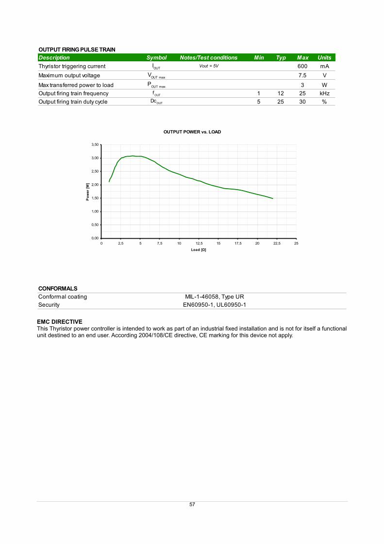
EMC DIRECTIVEThis Thyristor power controller is intended to work as part of an industrial fixed installation and is not for itself a functionalunit destined to an end user. According 2004/108/CE directive, CE marking for this device not apply.
57
CONFORMALS
Security EN60950-1, UL60950-1Conformal coating MIL-1-46058, Type UR
OUTPUT FIRING PULSE TRAIN
Description Symbol Notes/Test conditions Min Typ Max Units
Thyristor triggering current Vout = 5V 600 mA
Maximum output voltage 7.5 V
Max transferred power to load 3 W
Output firing train frequency 1 12 25 kHz
Output firing train duty cycle 5 25 30 %
IOUT
VOUT max
POUT max
fOUT
DcOUT
OUTPUT POWER vs. LOAD
0,00
0,50
1,00
1,50
2,00
2,50
3,00
3,50
0 2,5 5 7,5 10 12,5 15 17,5 20 22,5 25
Load [Ω]
Po
wer
[W
]

10.1 Mechanical dimensions
(All dimensions in mm)
10.2 Connectors overview
58
figure 41: Connectors overview of SC6006.
SE
MIC
OD
EE
LE
CT
RO
NIC
A
®
SC
6006
3 8 9 10 11 12 13 14 15 16 17 18 19 20 214 5 6 7 22
N RST
PWR
RESET
EXT BLKOV CURRFAULTFIRING
SC6006
G6 K6K5G5K4G4K3G3K2G2K1G1
MENU OK
A LPHAU_SE NSI_SE NSU_S ETI_SE TI_SENSU_SENS
LCD
CO
NT
RA
ST
COARSE FINE
1 2
J11 - SYNCHRONISMCONNECTOR
OUTPUT SCR FIRINGCONNECTORS
SIGNALING LEDS
J32 - DB-9 (DCE) RS-232COM CONNECTOR
J16 - FEEDBACK ANDALPHA SETPOINT
J15 - SETPOINTSAND INHIBIT
J14 - CURRENTINPUT FEEDBACK
J13 - EXTERNAL BLOCKAND DRY OUTPUT FAULT
J12 - FEEDBACKVOLTAGE
J1 - POWERSUPPLY
Description Notes/Test conditions UnitsBoard mm
Fixations fixation holes diameter 4.5 mm
Weight (aprox) 700 gr
225 x 170 x 45
SE
MIC
OD
EE
LEC
TR
ON
ICA
®
SC
6006
3 8 9 10 11 12 13 14 15 16 17 18 19 20 214 5 6 7 22
N RST
PWR
RESET
EXT BLKOV CURR
FAULTFIRING
SC6006
G6 K6K5G5K4G4K3G3K2G2K1G1
MENU OK
ALPHAU_SENSI_SENSU_SETI_SETI_SENSU_SENS
LCD
CO
NT
RA
ST
COARSE FINE
1 2

Cost Effective Products
SEMICODE ELECTRONICA
Offers to the market a comprehensive range of products from recognized manufacturers at the bestprice/quality relationship, this products are provided with a basic reference code that allows maintaining thesame product reference even if the original device manufacturer is replaced. SEMICODE product referencehas to be considered as a generic brand.
Seeking the market needs and trends, we are constantly increasing the product portfolio with new productsand suppliers, please ask for the updated information available to our local contacts.
SEMICODE products include semiconductors, passive components and accessories focused in powerelectronics market.
Datasheet Annotations:
SEMICODE ELECTRONICA annotate datasheets in the top left hard corner of the front page, to indicateproduct status. The annotations are as follows:Tentative information: This is the most tentative form of information and represents a very preliminaryspecification. No actual design work on the product has been started.Preliminary Information: The product is in design and development. The datasheet represents the productas it is understood but details may change.Advance Information: The product design is complete and final characterisation for volume production iswell in hand.No Annotation: The product parameters are fixed and the product is available to datasheet specification.
NOTICE: The technical data are to specify components, not to guarantee their properties.No warranty or guarantee expressed orimplied is made regarding delivery or performance. The Company reserves the right to alter without prior notice the specification of anyproduct. Information concerning possible methods of use is provided as a guide only and does not constitute any guarantee that suchmethods of use will be satisfactory in a specific piece of equipment. It is the user’s responsibility to fully determine the performance andsuitability of any equipment using such information and to ensure that any publication or data used is up to date.
All brand names and product names used in this publication are trademarks, registered trademarks or trade names of their respective owners.
© SEMICODE ELECTRONICA 2013. TECHNICAL DOCUMENTATION – NOT FOR RESALE
59
1303
20 R
ev.:2
.3