SBAS290B − JULY 2003 − SEPTEMBER 2004 High … · SBAS290B − JULY 2003 − SEPTEMBER 2004...
31
SBAS290B - JULY 2003 - SEPTEMBER 2004 High-Performance 24-Bit, 216kHz Sampling Stereo Audio Analog-to-Digital Converter PCM4202 FEATURES D Two High-Performance Delta-Sigma Analog-to-Digital Converters - 24-Bit Linear PCM or 1-Bit Direct Stream Digital (DSD) Output Data - Supports PCM Output Sampling Rates up to 216kHz - Supports 64f S and 128f S DSD Output Data Rates D Dynamic Performance: PCM Output - Dynamic Range (V IN = -60dBFS, f IN = 1kHz, A-Weighted): 118dB - THD+N (V IN = -0.5dB, f IN = 1kHz): -105dB D Dynamic Performance: DSD Output, 64f S - Dynamic Range (A-Weighted): 115dB - THD+N (V IN = -0.5dB, f IN = 1kHz): -102dB D Audio Serial Port - 24-Bit Linear PCM Output Data - Master or Slave Mode Operation - Supports Left-Justified, Right-Justified, and I 2 SE Data Formats D Additional PCM Output Features: - Linear-Phase Digital Decimation Filter - Digital High-Pass Filter for DC Removal - Clipping Flag Output for Each Channel D Power Supplies: +5V Analog and +3.3V Digital D Power Dissipation: - f S = 48kHz: 308mW typical - f S = 96kHz: 338mW typical - f S = 192kHz: 318mW typical D Power-Down Mode D Available in a SSOP-28 Package D Pin- and Function-Compatible with the PCM1804 APPLICATIONS D Digital Recorders and Mixing Desks D Digital Audio Effects Processors D Broadcast Studio Equipment D Surround-Sound Encoders D High-End A/V Receivers DESCRIPTION The PCM4202 is a high-performance, stereo audio analog-to-digital (A/D) converter designed for professional and broadcast audio applications. The PCM4202 architecture utilizes a 1-bit delta-sigma modulator per channel, incorporating a novel density modulated dither scheme for improved dynamic performance. The PCM4202 supports 24-bit linear PCM output data, with sampling frequencies up to 216kHz. The PCM4202 can also be configured to output either 64x or 128x oversampled, 1-bit direct stream digital (DSD) data for each channel. Support for PCM and DSD output formats makes the PCM4202 suitable for a variety of digital audio recording and processing applications. The PCM4202 includes a flexible audio serial port inter- face, which supports standard audio data formats. Audio data format selection, sampling mode configuration, and high-pass filter functions are all programmed using dedi- cated control pins. The PCM4202 operates from a +5V analog power supply and a +3.3V digital power supply. The digital I/O pins are compatible with +3.3V logic families. The PCM4202 is available in a small SSOP-28 package. I 2 S is a registered trademark of Royal Philips Electronics B.V., The Netherlands. All other trademarks are the property of their respective owners. PRODUCTION DATA information is current as of publication date. Products conform to specifications per the terms of Texas Instruments standard warranty. Production processing does not necessarily include testing of all parameters. www.ti.com Copyright 2003-2004, Texas Instruments Incorporated Please be aware that an important notice concerning availability, standard warranty, and use in critical applications of Texas Instruments semiconductor products and disclaimers thereto appears at the end of this data sheet.
Transcript of SBAS290B − JULY 2003 − SEPTEMBER 2004 High … · SBAS290B − JULY 2003 − SEPTEMBER 2004...
SBAS290B − JULY 2003 − SEPTEMBER 2004
High-Performance 24-Bit, 216kHz SamplingStereo Audio Analog-to-Digital Converter
FEATURES Two High-Performance Delta-Sigma
Analog-to-Digital Converters− 24-Bit Linear PCM or 1-Bit Direct Stream
Digital (DSD) Output Data− Supports PCM Output Sampling Rates up
to 216kHz− Supports 64f S and 128f S DSD Output Data
Rates Dynamic Performance: PCM Output
− Dynamic Range (V IN = −60dBFS,fIN = 1kHz, A-Weighted): 118dB
− THD+N (VIN = −0.5dB, f IN = 1kHz): −105dB Dynamic Performance: DSD Output, 64f S
− Dynamic Range (A-Weighted): 115dB− THD+N (VIN = −0.5dB, f IN = 1kHz): −102dB
Audio Serial Port− 24-Bit Linear PCM Output Data− Master or Slave Mode Operation− Supports Left-Justified, Right-Justified,
and I2S Data Formats Additional PCM Output Features:
− Linear-Phase Digital Decimation Filter− Digital High-Pass Filter for DC Removal− Clipping Flag Output for Each Channel
Power Supplies: +5V Analog and +3.3V Digital Power Dissipation:
− fS = 48kHz: 308mW typical− fS = 96kHz: 338mW typical− fS = 192kHz: 318mW typical
Power-Down Mode Available in a SSOP-28 Package Pin- and Function-Compatible with the
PCM1804
APPLICATIONS Digital Recorders and Mixing Desks Digital Audio Effects Processors Broadcast Studio Equipment Surround-Sound Encoders High-End A/V Receivers
DESCRIPTION
The PCM4202 is a high-performance, stereo audioanalog-to-digital (A/D) converter designed for professionaland broadcast audio applications. The PCM4202architecture utilizes a 1-bit delta-sigma modulator perchannel, incorporating a novel density modulated ditherscheme for improved dynamic performance.
The PCM4202 supports 24-bit linear PCM output data,with sampling frequencies up to 216kHz. The PCM4202can also be configured to output either 64x or 128xoversampled, 1-bit direct stream digital (DSD) data foreach channel. Support for PCM and DSD output formatsmakes the PCM4202 suitable for a variety of digital audiorecording and processing applications.The PCM4202 includes a flexible audio serial port inter-face, which supports standard audio data formats. Audiodata format selection, sampling mode configuration, andhigh-pass filter functions are all programmed using dedi-cated control pins.
The PCM4202 operates from a +5V analog power supplyand a +3.3V digital power supply. The digital I/O pins arecompatible with +3.3V logic families. The PCM4202 isavailable in a small SSOP-28 package.
I2S is a registered trademark of Royal Philips Electronics B.V., The Netherlands. All other trademarks are the property of their respective owners.
! " #$ % $ %
www.ti.com
Copyright 2003−2004, Texas Instruments Incorporated
Please be aware that an important notice concerning availability, standard warranty, and use in critical applications of Texas Instrumentssemiconductor products and disclaimers thereto appears at the end of this data sheet.
SBAS290B − JULY 2003 − SEPTEMBER 2004
www.ti.com
2
This integrated circuit can be damaged by ESD. Texas Instruments recommends that all integrated circuits be handled with appropriateprecautions. Failure to observe proper handling and installation procedures can cause damage.
ESD damage can range from subtle performance degradation to complete device failure. Precision integrated circuits may be more susceptible todamage because very small parametric changes could cause the device not to meet its published specifications.
ABSOLUTE MAXIMUM RATINGSover operating free-air temperature range unless otherwise noted(1)
PCM4202 UNIT
Supply voltageVCC +6.0 V
Supply voltageVDD +3.6 V
Ground voltage differences (any AGND to DGND) ±0.1 V
Digital input voltageFMT0, FMT1, S/M, FS0, FS1, FS2, SCKI,RST, HPFD, BCK, LRCK
−0.3 to (VDD + 0.3) V
Analog input voltage VINL+, VINL−, VINR+, VINR− −0.3 to (VCC + 0.3) V
Input current (any pin except supplies) ±10mA V
Operating temperature range −10 to +70 °C
Storage temperature range, TSTG −65 to +150 °C(1) Stresses above those listed under Absolute Maximum Ratings may cause permanent damage to the device. Exposure to absolute maximum
conditions for extended periods may degrade device reliability. These are stress ratings only, and functional operation of the device at these orany other conditions beyond those specified is not implied.
PACKAGE/ORDERING INFORMATIONFor the most current package and ordering information, see the Package Option Addendum located at the end of thisdatasheet.
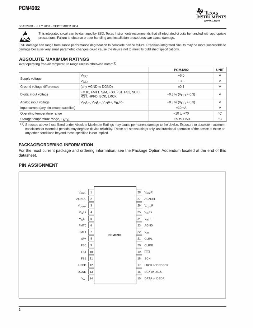
PIN ASSIGNMENT
VREFL
AGNDL
VCOML
VINL+
VINL−
FMT0
FMT1
S/M
FS0
FS1
FS2
HPFD
DGND
VDD
VREFR
AGNDR
VCOMR
VINR+
VINR−
AGND
VCC
CLIPL
CLIPR
RST
SCKI
LRCK or DSDBCK
BCK or DSDL
DATA or DSDR
1
2
3
4
5
6
7
8
9
10
11
12
13
14
28
27
26
25
24
23
22
21
20
19
18
17
16
15
PCM4202

SBAS290B − JULY 2003 − SEPTEMBER 2004
www.ti.com
3
Terminal Functions TERMINAL
PIN NO. NAME I/O DESCRIPTION
1 VREFL Output Left Channel Voltage Reference
2 AGNDL Ground Left Channel Reference Ground
3 VCOML Output Left Channel DC Common-mode Voltage, +2.5V Typical
4 VINL+ Input Left Channel Non-inverting Analog Input
5 VINL− Input Left Channel Inverting Analog Input
6 FMT0 Input Audio Data Format Selection
7 FMT1 Input Audio Data Format Selection
8 S/M Input Audio Serial Port Slave/Master Mode Selection (0 = Master, 1 = Slave)
9 FS0 Input Sampling Mode Selection
10 FS1 Input Sampling Mode Selection
11 FS2 Input Sampling Mode Selection
12 HPFD Input High-pass Filter Disable (Active High)
13 DGND Ground Digital Ground
14 VDD Power Digital Power Supply, +3.3V
15 DATAor DSDR
Output Audio Serial Port Left and Right Channel PCM Dataor Right Channel DSD Data
16 BCKor DSDL
I/O Audio Serial Port Bit (or Data) Clockor Left Channel DSD Data Output
17 LRCKor DSDBCK
I/O Audio Serial Port Left/Right (or Word) Clockor DSD Data Clock Output
18 SCKI Input System Clock
19 RST Input Reset/Power-down (Active Low with internal pull-up)
20 CLIPR Output Right Channel Clipping Flag (Active High)
21 CLIPL Output Left Channel Clipping Flag (Active High)
22 VCC Power Analog Power Supply, +5V
23 AGND Ground Analog Ground
24 VINR− Input Right Channel Inverting Analog Input
25 VINR+ Input Right Channel Non-inverting Analog Input
26 VCOMR Output Right Channel DC Common-mode Voltage, +2.5V Typical
27 AGNDR Ground Right Channel Reference Ground
28 VREFR Output Right Channel Voltage Reference
SBAS290B − JULY 2003 − SEPTEMBER 2004
www.ti.com
4
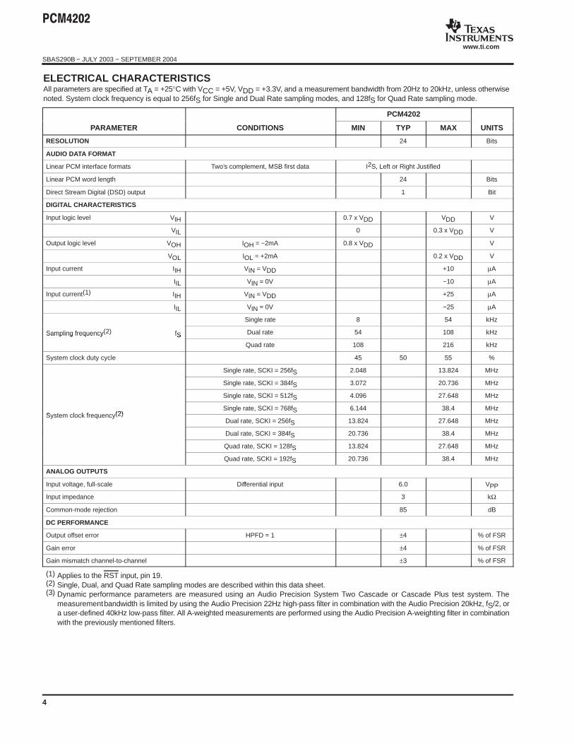
ELECTRICAL CHARACTERISTICS All parameters are specified at TA = +25°C with VCC = +5V, VDD = +3.3V, and a measurement bandwidth from 20Hz to 20kHz, unless otherwisenoted. System clock frequency is equal to 256fS for Single and Dual Rate sampling modes, and 128fS for Quad Rate sampling mode.
PCM4202
PARAMETER CONDITIONS MIN TYP MAX UNITS
RESOLUTION 24 Bits
AUDIO DATA FORMAT
Linear PCM interface formats Two’s complement, MSB first data I2S, Left or Right Justified
Linear PCM word length 24 Bits
Direct Stream Digital (DSD) output 1 Bit
DIGITAL CHARACTERISTICS
Input logic level VIH 0.7 x VDD VDD V
VIL 0 0.3 x VDD V
Output logic level VOH IOH = −2mA 0.8 x VDD V
VOL IOL = +2mA 0.2 x VDD V
Input current IIH VIN = VDD +10 µA
IIL VIN = 0V −10 µA
Input current(1) IIH VIN = VDD +25 µA
IIL VIN = 0V −25 µA
Single rate 8 54 kHz
Sampling frequency(2) fS Dual rate 54 108 kHzSampling frequency fS
Quad rate 108 216 kHz
System clock duty cycle 45 50 55 %
Single rate, SCKI = 256fS 2.048 13.824 MHz
Single rate, SCKI = 384fS 3.072 20.736 MHz
Single rate, SCKI = 512fS 4.096 27.648 MHz
System clock frequency(2)Single rate, SCKI = 768fS 6.144 38.4 MHz
System clock frequency(2)Dual rate, SCKI = 256fS 13.824 27.648 MHz
Dual rate, SCKI = 384fS 20.736 38.4 MHz
Quad rate, SCKI = 128fS 13.824 27.648 MHz
Quad rate, SCKI = 192fS 20.736 38.4 MHz
ANALOG OUTPUTS
Input voltage, full-scale Differential input 6.0 VPP
Input impedance 3 kΩ
Common-mode rejection 85 dB
DC PERFORMANCE
Output offset error HPFD = 1 ±4 % of FSR
Gain error ±4 % of FSR
Gain mismatch channel-to-channel ±3 % of FSR
(1) Applies to the RST input, pin 19.(2) Single, Dual, and Quad Rate sampling modes are described within this data sheet.(3) Dynamic performance parameters are measured using an Audio Precision System Two Cascade or Cascade Plus test system. The
measurement bandwidth is limited by using the Audio Precision 22Hz high-pass filter in combination with the Audio Precision 20kHz, fS/2, ora user-defined 40kHz low-pass filter. All A-weighted measurements are performed using the Audio Precision A-weighting filter in combinationwith the previously mentioned filters.
SBAS290B − JULY 2003 − SEPTEMBER 2004
www.ti.com
5
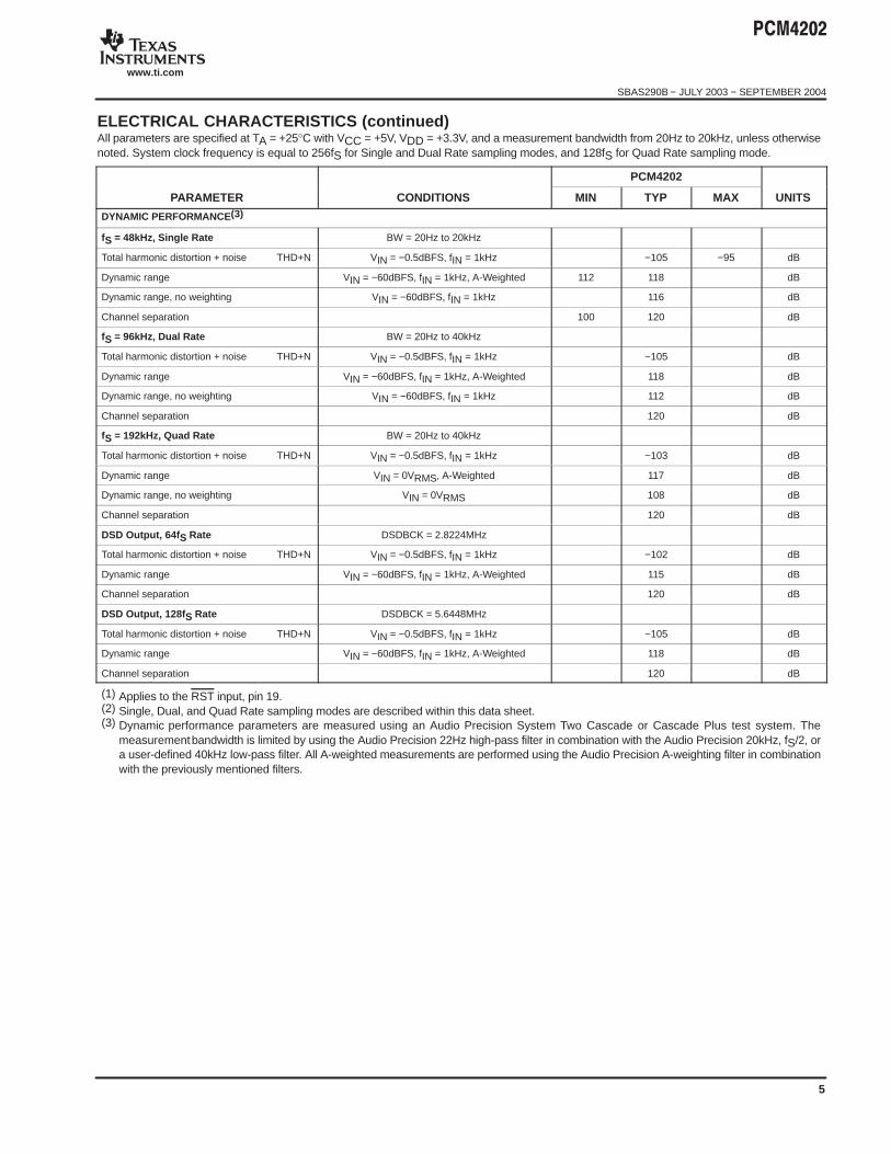
ELECTRICAL CHARACTERISTICS (continued)All parameters are specified at TA = +25°C with VCC = +5V, VDD = +3.3V, and a measurement bandwidth from 20Hz to 20kHz, unless otherwisenoted. System clock frequency is equal to 256fS for Single and Dual Rate sampling modes, and 128fS for Quad Rate sampling mode.
PCM4202
PARAMETER UNITSMAXTYPMINCONDITIONS
DYNAMIC PERFORMANCE(3)
fS = 48kHz, Single Rate BW = 20Hz to 20kHz
Total harmonic distortion + noise THD+N VIN = −0.5dBFS, fIN = 1kHz −105 −95 dB
Dynamic range VIN = −60dBFS, fIN = 1kHz, A-Weighted 112 118 dB
Dynamic range, no weighting VIN = −60dBFS, fIN = 1kHz 116 dB
Channel separation 100 120 dB
fS = 96kHz, Dual Rate BW = 20Hz to 40kHz
Total harmonic distortion + noise THD+N VIN = −0.5dBFS, fIN = 1kHz −105 dB
Dynamic range VIN = −60dBFS, fIN = 1kHz, A-Weighted 118 dB
Dynamic range, no weighting VIN = −60dBFS, fIN = 1kHz 112 dB
Channel separation 120 dB
fS = 192kHz, Quad Rate BW = 20Hz to 40kHz
Total harmonic distortion + noise THD+N VIN = −0.5dBFS, fIN = 1kHz −103 dB
Dynamic range VIN = 0VRMS, A-Weighted 117 dB
Dynamic range, no weighting VIN = 0VRMS 108 dB
Channel separation 120 dB
DSD Output, 64f S Rate DSDBCK = 2.8224MHz
Total harmonic distortion + noise THD+N VIN = −0.5dBFS, fIN = 1kHz −102 dB
Dynamic range VIN = −60dBFS, fIN = 1kHz, A-Weighted 115 dB
Channel separation 120 dB
DSD Output, 128f S Rate DSDBCK = 5.6448MHz
Total harmonic distortion + noise THD+N VIN = −0.5dBFS, fIN = 1kHz −105 dB
Dynamic range VIN = −60dBFS, fIN = 1kHz, A-Weighted 118 dB
Channel separation 120 dB
(1) Applies to the RST input, pin 19.(2) Single, Dual, and Quad Rate sampling modes are described within this data sheet.(3) Dynamic performance parameters are measured using an Audio Precision System Two Cascade or Cascade Plus test system. The
measurement bandwidth is limited by using the Audio Precision 22Hz high-pass filter in combination with the Audio Precision 20kHz, fS/2, ora user-defined 40kHz low-pass filter. All A-weighted measurements are performed using the Audio Precision A-weighting filter in combinationwith the previously mentioned filters.
SBAS290B − JULY 2003 − SEPTEMBER 2004
www.ti.com
6
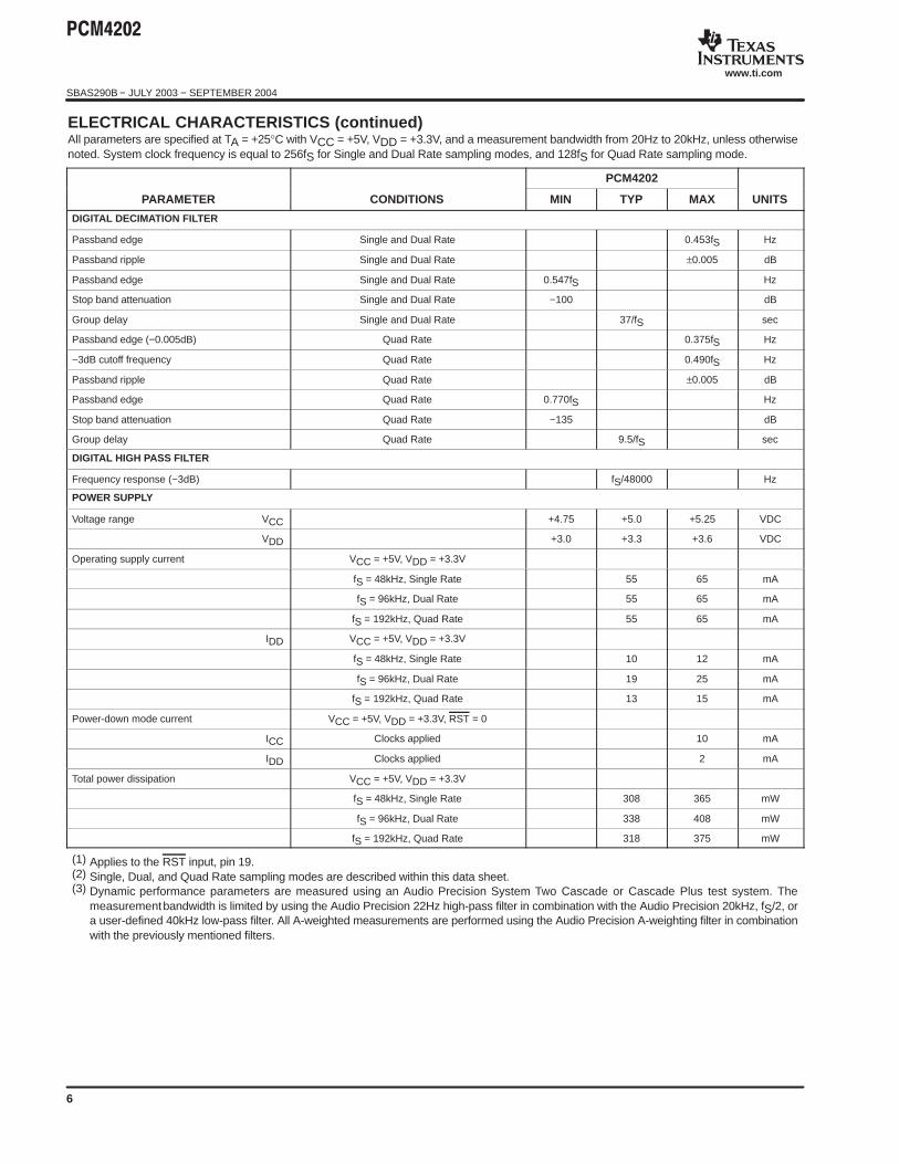
ELECTRICAL CHARACTERISTICS (continued)All parameters are specified at TA = +25°C with VCC = +5V, VDD = +3.3V, and a measurement bandwidth from 20Hz to 20kHz, unless otherwisenoted. System clock frequency is equal to 256fS for Single and Dual Rate sampling modes, and 128fS for Quad Rate sampling mode.
PCM4202
PARAMETER UNITSMAXTYPMINCONDITIONS
DIGITAL DECIMATION FILTER
Passband edge Single and Dual Rate 0.453fS Hz
Passband ripple Single and Dual Rate ±0.005 dB
Passband edge Single and Dual Rate 0.547fS Hz
Stop band attenuation Single and Dual Rate −100 dB
Group delay Single and Dual Rate 37/fS sec
Passband edge (−0.005dB) Quad Rate 0.375fS Hz
−3dB cutoff frequency Quad Rate 0.490fS Hz
Passband ripple Quad Rate ±0.005 dB
Passband edge Quad Rate 0.770fS Hz
Stop band attenuation Quad Rate −135 dB
Group delay Quad Rate 9.5/fS sec
DIGITAL HIGH PASS FILTER
Frequency response (−3dB) fS/48000 Hz
POWER SUPPLY
Voltage range VCC +4.75 +5.0 +5.25 VDC
VDD +3.0 +3.3 +3.6 VDC
Operating supply current VCC = +5V, VDD = +3.3V
fS = 48kHz, Single Rate 55 65 mA
fS = 96kHz, Dual Rate 55 65 mA
fS = 192kHz, Quad Rate 55 65 mA
IDD VCC = +5V, VDD = +3.3V
fS = 48kHz, Single Rate 10 12 mA
fS = 96kHz, Dual Rate 19 25 mA
fS = 192kHz, Quad Rate 13 15 mA
Power-down mode current VCC = +5V, VDD = +3.3V, RST = 0
ICC Clocks applied 10 mA
IDD Clocks applied 2 mA
Total power dissipation VCC = +5V, VDD = +3.3V
fS = 48kHz, Single Rate 308 365 mW
fS = 96kHz, Dual Rate 338 408 mW
fS = 192kHz, Quad Rate 318 375 mW
(1) Applies to the RST input, pin 19.(2) Single, Dual, and Quad Rate sampling modes are described within this data sheet.(3) Dynamic performance parameters are measured using an Audio Precision System Two Cascade or Cascade Plus test system. The
measurement bandwidth is limited by using the Audio Precision 22Hz high-pass filter in combination with the Audio Precision 20kHz, fS/2, ora user-defined 40kHz low-pass filter. All A-weighted measurements are performed using the Audio Precision A-weighting filter in combinationwith the previously mentioned filters.
SBAS290B − JULY 2003 − SEPTEMBER 2004
www.ti.com
7
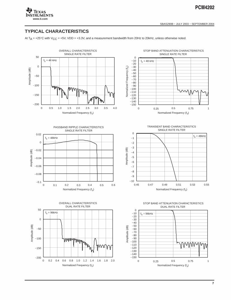
TYPICAL CHARACTERISTICSAt TA = +25°C with VCC = +5V, VDD = +3.3V, and a measurement bandwidth from 20Hz to 20kHz, unless otherwise noted.
OVERALL CHARACTERISTICSSINGLE RATE FILTER
−200
−150
−100
−50
0
50
0 0.5 1.0 1.5 2.0 2.5 3.0 3.5 4.0
Normalized Frequency (fS)
Am
plit
ude
(dB
)
fS = 48 kHz
STOP BAND ATTENUATION CHARACTERISTICSSINGLE RATE FILTER
0−10−20−30−40−50−60−70−80−90
−100−110−120−130−140−150
0 0.25 0.5 0.75 1
Normalized Frequency (fS)
No
rma
lized
Fre
que
ncy
(fS)
fS = 48 kHz
PASSBAND RIPPLE CHARACTERISTICSSINGLE RATE FILTER
0.02
0
−0.02
−0.04
−0.06
−0.08
−0.10 0.1 0.2 0.3 0.4 0.5 0.6
Normalized Frequency (fS)
Am
plit
ude
(dB
)
fS = 48kHz
TRANSIENT BAND CHARACTERISTICSSINGLE RATE FILTER
Normalized Frequency (fS)
fS = 48kHz
Am
plitu
de
(dB
)
0
−1
−2
−3
−4
−5
−6
−7
−8
−9
−100.510.490.470.45 0.53 0.55
OVERALL CHARACTERISTICSDUAL RATE FILTER
Normalized Frequency (fS)
Am
plitu
de(d
B)
50
0
−50
−100
−150
−2000.2 0.4 0.6 0.8 1.0 1.2 1.4 1.6 1.8 2.00
fS = 96kHz
STOP BAND ATTENUATION CHARACTERISTICSDUAL RATE FILTER
0 0.25 0.5 0.75 1
Normalized Frequency (fS)
Am
plitu
de
(dB
)
fS = 96kHz0
−10−20−30−40−50−60−70−80−90
−100−110−120−130−140−150
SBAS290B − JULY 2003 − SEPTEMBER 2004
www.ti.com
8
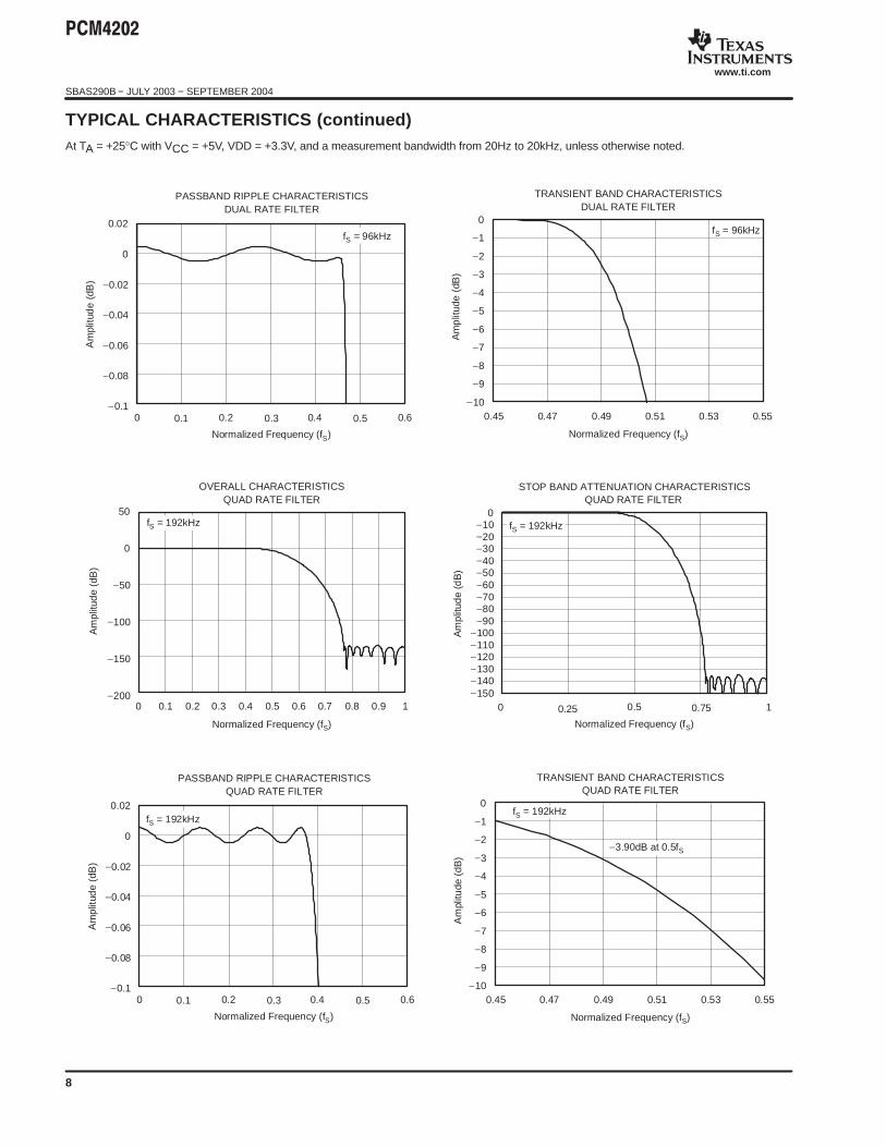
TYPICAL CHARACTERISTICS (continued)At TA = +25°C with VCC = +5V, VDD = +3.3V, and a measurement bandwidth from 20Hz to 20kHz, unless otherwise noted.
PASSBAND RIPPLE CHARACTERISTICSDUAL RATE FILTER
0.02
0
−0.02
−0.04
−0.06
−0.08
−0.10 0.1 0.2 0.3 0.4 0.5 0.6
Normalized Frequency (fS)
Am
plitu
de
(dB
)
fS = 96kHz
TRANSIENT BAND CHARACTERISTICSDUAL RATE FILTER
Normalized Frequency (fS)
fS = 96kHz
Am
plit
ude
(dB
)
0
−1
−2
−3
−4
−5
−6
−7
−8
−9
−100.510.490.470.45 0.53 0.55
OVERALL CHARACTERISTICSQUAD RATE FILTER
Normalized Frequency (fS)
50
0
−50
−100
−150
−2000.1 0.2 0.3 0.4 0.5 0.6 0.7 0.8 0.9 10
fS = 192kHz
Am
plitu
de
(dB
)
STOP BAND ATTENUATION CHARACTERISTICSQUAD RATE FILTER
0 0.25 0.5 0.75 1
Normalized Frequency (fS)
Am
plitu
de
(dB
)
fS = 192kHz0
−10−20−30−40−50−60−70−80−90
−100−110−120−130−140−150
PASSBAND RIPPLE CHARACTERISTICSQUAD RATE FILTER
0.02
0
−0.02
−0.04
−0.06
−0.08
−0.10 0.1 0.2 0.3 0.4 0.5 0.6
Normalized Frequency (fS)
Am
plitu
de
(dB
)
fS = 192kHz
TRANSIENT BAND CHARACTERISTICSQUAD RATE FILTER
Normalized Frequency (fS)
Am
plitu
de(d
B)
0
−1
−2
−3
−4
−5
−6
−7
−8
−9
−100.510.490.470.45 0.53 0.55
fS = 192kHz
−3.90dB at 0.5fS
SBAS290B − JULY 2003 − SEPTEMBER 2004
www.ti.com
9
TYPICAL CHARACTERISTICS (continued)At TA = +25°C with VCC = +5V, VDD = +3.3V, and a measurement bandwidth from 20Hz to 20kHz, unless otherwise noted.
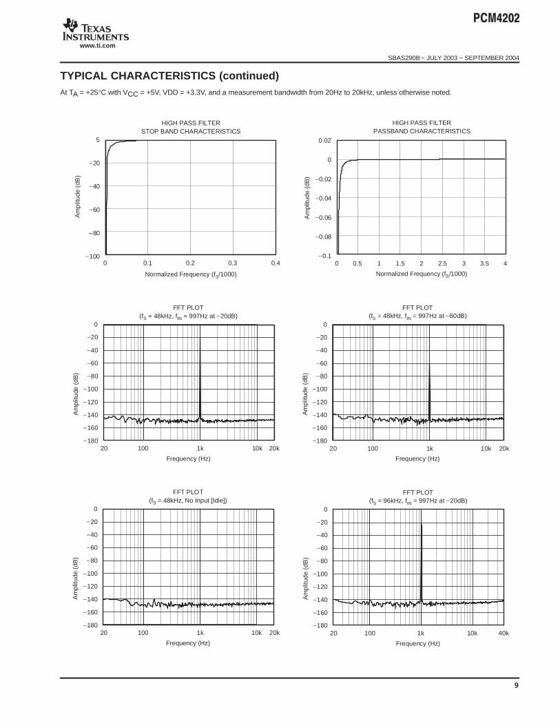
HIGH PASS FILTERSTOP BAND CHARACTERISTICS
Normalized Frequency (fS/1000)
Am
plit
ude
(dB
)
5
−20
−40
−60
−80
−1000.1 0.2 0.3 0.40
HIGH PASS FILTERPASSBAND CHARACTERISTICS
0.02
0
−0.02
−0.04
−0.06
−0.08
−0.1
Normalized Frequency (fS/1000)
Am
plitu
de
(dB
)
0 0.5 1 1.5 2 2.5 3 3.5 4
FFT PLOT(fS = 48kHz, fIN = 997Hz at −20dB)
Frequency (Hz)
Am
plitu
de(d
B)
0
−20
−40
−60
−80
−100
−120
−140
−160
−1801k10020 10k 20k
FFT PLOT(fS = 48kHz, fIN = 997Hz at −60dB)
Frequency (Hz)
Am
plitu
de(d
B)
0
−20
−40
−60
−80
−100
−120
−140
−160
−1801k10020 10k 20k
FFT PLOT(fS = 48kHz, No Input [Idle])
Frequency (Hz)
Am
plitu
de(d
B)
0
−20
−40
−60
−80
−100
−120
−140
−160
−1801k10020 10k 20k
FFT PLOT(fS = 96kHz, fIN = 997Hz at −20dB)
Frequency (Hz)
Am
plit
ude
(dB
)
0
−20
−40
−60
−80
−100
−120
−140
−160
−1801k10020 10k 40k
SBAS290B − JULY 2003 − SEPTEMBER 2004
www.ti.com
10
TYPICAL CHARACTERISTICS (continued)At TA = +25°C with VCC = +5V, VDD = +3.3V, and a measurement bandwidth from 20Hz to 20kHz, unless otherwise noted.
FFT PLOT(fS = 96kHz, fIN = 997Hz at −60dB)
Frequency (Hz)
Am
plit
ude
(dB
)
0
−20
−40
−60
−80
−100
−120
−140
−160
−1801k10020 10k 40k
FFT PLOT(fS = 96kHz, No Input [Idle])
Frequency (Hz)
Am
plitu
de(d
B)
0
−20
−40
−60
−80
−100
−120
−140
−160
−1801k10020 10k 40k
FFT PLOT(fS = 192kHz, fIN = 997Hz at −20dB)
Frequency (Hz)
Am
plit
ude
(dB
)
0
−20
−40
−60
−80
−100
−120
−140
−160
−1801k10020 10k 100k
FFT PLOT(fS = 192kHz, fIN = 997Hz at −60dB)
Frequency (Hz)
Am
plitu
de
(dB
)
0
−20
−40
−60
−80
−100
−120
−140
−160
−1801k10020 10k 100k
FFT PLOT(fS = 192kHz, No Input [Idle])
Frequency (Hz)
Am
plitu
de(d
B)
0
−20
−40
−60
−80
−100
−120
−140
−160
−1801k10020 10k 100k
THD+N vs AMPLITUDE(fS = 48kHz, fIN = 1kHz, BW = 10Hz to 20kHz)
Input Amplitude (dB)
TH
D+
N(d
B)
−90−92−94−96−98
−100−102−104−106−108−110−112−114−116−118−120
−80 −60−120 −100−140 −40 −20 0

SBAS290B − JULY 2003 − SEPTEMBER 2004
www.ti.com
11
TYPICAL CHARACTERISTICS (continued)At TA = +25°C with VCC = +5V, VDD = +3.3V, and a measurement bandwidth from 20Hz to 20kHz, unless otherwise noted.
THD+N vs FREQUENCY(fS = 48kHz, Input Amplitude = −0.5dB,
BW = 10Hz to 20kHz)
Input Frequency (Hz)
TH
D+
N(d
B)
−90−92−94−96−98
−100−102−104−106−108−110−112−114−116−118−120
1k10020 10k 20k
THD+N vs AMPLITUDE(fS = 96kHz, fIN = 1kHz, BW = 10Hz to 40kHz)
Input Amplitude (dB)
TH
D+
N(d
B)
−90−92−94−96−98
−100−102−104−106−108−110−112−114−116−118−120
−80 −60−120 −100−140 −40 −20 0
THD+N vs FREQUENCY(fS = 96kHz, Input Amplitude = −0.5dB,
BW = 10Hz to 40kHz)
Input Frequency (Hz)
TH
D+
N(d
B)
−90−92−94−96−98
−100−102−104−106−108−110−112−114−116−118−120
1k10020 10k 40k
THD+N vs AMPLITUDE(fS = 192kHz, fIN = 1kHz, BW = 10Hz to 40kHz)
Input Amplitude (dB)
TH
D+
N(d
B)
−90−92−94−96−98
−100−102−104−106−108−110−112−114−116−118−120
−80 −60−120 −100−140 −40 −20 0
THD+N vs FREQUENCY(fS = 192kHz, Input Amplitude = −0.5dB,
BW = 10Hz to 40kHz)
Input Frequency (Hz)
TH
D+
N(d
B)
−90−92−94−96−98
−100−102−104−106−108−110−112−114−116−118−120
1k10020 10k 80k

SBAS290B − JULY 2003 − SEPTEMBER 2004
www.ti.com
12
PRODUCT OVERVIEWThe PCM4202 is a high-performance, stereo audioanalog-to-digital (A/D) converter designed for use inprofessional and broadcast audio applications. ThePCM4202 features 24-bit linear PCM or 1-bit DirectStream Digital (DSD) data output capability for bothchannels. Sampling rates up to 216kHz are supported forPCM output formats, while 64x or 128x oversampled 1-bitdata is supported for DSD output mode. Native support forboth PCM and DSD data formats makes the PCM4202ideal for use in a wide variety of audio recording andprocessing applications.
The PCM4202 features 1-bit delta-sigma modulatorsemploying density modulated dither for improved dynamicperformance. Differential voltage inputs are utilized for themodulators, providing excellent common-mode rejection.On-chip voltage references are provided for the
modulators, in addition to generating DC common-modebias voltage outputs for use with external input circuitry.Linear phase digital decimation filtering is provided for the24-bit PCM data outputs, with a minimum stop bandattenuation of −100dB for all sampling modes.
The PCM output mode features clipping flag outputs foreach channel, as well as a digital high-pass filter for DCremoval. The PCM4202 may be configured usingdedicated input pins for sampling mode and audio dataformat selection, high-pass filter enable/disable, andreset/power-down operation.
A +5V power supply is required for the analog section ofthe device, while a +3.3V power supply is required for thedigital circuitry. Figure 1 shows the functional blockdiagram for the PCM4202.
HPFDelta−SigmaModulator
DecimationFilter
VoltageReference
VCOMR
AGNDR
VREFR
VINR+
VINR−
Power
VDDAGND
ResetLogic
ClockControl
AudioSerialPort
DGNDVCC
LRCKor DSDBCK
BCKor DSDL
DATAor DSDR
S/M
FMT0
FMT1
CLIPR
CLIPL
HPFDelta−SigmaModulator
DecimationFilter
VoltageReference
VREFL
AGNDL
VCOML
VINL−
VINL+
FS1
FS2
SCKI
RST
HPFD
FS0
Figure 1. PCM4202 Functional Block Diagram
SBAS290B − JULY 2003 − SEPTEMBER 2004
www.ti.com
13
ANALOG INPUTS
The PCM4202 includes two channels of A/D conversion,each with its own pair of differential voltage input pins. TheVINL+ (pin 4) and VINL− (pin 5) inputs correspond to Leftchannel input, while VINR+ (pin 25) and VINR− (pin 24)correspond to the Right channel input. The average inputimpedance of each input pin is 3kΩ.
Each analog input pair accepts a full-scale input voltage ofapproximately 6.0VPP differential, which corresponds to a2.12VRMS or +8.75dBu input swing. The analog inputshould not swing below analog ground or above the VCCpower supply by more than 300mV. Refer to theApplications Information section of this datasheet for anexample input buffer circuit.
VOLTAGE REFERENCES AND COMMON MODEBIAS VOLTAGE OUTPUTS
The PCM4202 includes two on-chip voltage references,one each for the Left and Right channels. The VREFL (pin1) and VREFR (pin 28) outputs correspond to highreference outputs for Left and Right channels,respectively. De-coupling capacitors are connectedbetween each of these pins and the correspondingreference ground pin, either AGNDL (pin 2) for the VREFLoutput or AGNDR (pin 27) for the VREFR output. It isrecommended to have at least a 0.1µF X7R ceramic chipcapacitor connected in parallel with a 33µF low ESRtantalum chip capacitor for de-coupling purposes. TheVREFL and VREFR outputs should not be utilized to biasexternal circuitry, because they are not buffered. Use theVCOML (pin 3) and VCOMR (pin 26) outputs to bias externalcircuitry, as described in the following paragraphs.
Refer to the Applications Information section of thisdatasheet for the recommended voltage reference pinconnections.
The PCM4202 analog inputs are internally biased toapproximately VCC/2. This bias voltage is referred to as thecommon mode voltage, and is output at VCOML (pin 3) andVCOMR (pin 26), corresponding to the Left and Rightchannels, respectively. These outputs provide a levelshifting voltage for biasing external input buffer circuitry.Although the VCOML and VCOMR outputs are internallybuffered, the output current is limited to a few hundred µA.It is recommended to connect these pins to external nodeswith greater than 1MΩ impedance, or to buffer the outputswith a voltage follower circuit when driving multipleexternal or low impedance nodes.
Refer to the Applications Information section of thisdatasheet for an example input buffer circuit that utilizesthe common-mode bias voltage outputs.
SYSTEM CLOCK INPUT
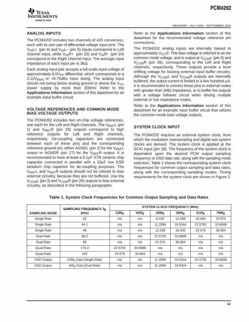
The PCM4202 requires an external system clock, fromwhich the modulator oversampling and digital sub-systemclocks are derived. The system clock is applied at theSCKI input (pin 18). The frequency of the system clock isdependent upon the desired PCM output samplingfrequency or DSD data rate, along with the sampling modeselection. Table 1 shows the corresponding system clockfrequencies for common output sampling and data rates,along with the corresponding sampling modes. Timingrequirements for the system clock are shown in Figure 2.
Table 1. System Clock Frequencies for Common Output Sampling and Data Rates
SAMPLING FREQUENCY, f SSYSTEM CLOCK FREQUENCY (MHz)
SAMPLING MODESAMPLING FREQUENCY, f S
(kHz) 128fS 192fS 256fS 384fS 512fS 768fS
Single Rate 32 n/a n/a 8.192 12.288 16.384 24.576
Single Rate 44.1 n/a n/a 11.2896 16.9344 22.5792 33.8688
Single Rate 48 n/a n/a 12.288 18.432 24.576 36.864
Dual Rate 88.2 n/a n/a 22.5792 33.8688 n/a n/a
Dual Rate 96 n/a n/a 24.576 36.864 n/a n/a
Quad Rate 176.4 22.5792 33.8688 n/a n/a n/a n/a
Quad Rate 192 24.576 36.864 n/a n/a n/a n/a
DSD Output 128fS Data (Single Rate) n/a n/a 11.2896 16.9344 22.5792 33.8688
DSD Output 64fS Data (Dual Rate) n/a n/a 11.2896 16.9344 n/a n/a

SBAS290B − JULY 2003 − SEPTEMBER 2004
www.ti.com
14
SCKI
t SCKI
t SCKIH
t SCKIL
PARAMETER DESCRIPTION MIN MAX UNITS
System Clock Period 26 ns
tSCKIH System Clock High Pulse Time 12 ns
tSCKIL System Clock Low Pulse Time 12 ns
tSCKI
Figure 2. System Clock Timing Requirements
SAMPLING MODES
The PCM4202 may be operated in one of three PCMsampling modes, or at one of two DSD output data rates.The PCM sampling modes are referred to as Single Rate,Dual Rate, and Quad Rate.
Single Rate mode is utilized for sampling rates up to54kHz. The delta-sigma modulator oversamples theanalog input signal by a rate equal to 128 times the desiredoutput sampling rate.
Dual Rate mode is utilized for sampling rates higher than54kHz and up to 108kHz. The delta-sigma modulatoroversamples the analog input signal by a rate equal to 64times the desired output sampling rate.
Quad Rate mode is utilized for sampling frequencieshigher than 108kHz and up to 216kHz. The delta-sigmamodulator oversamples the analog input signal by a rateequal to 32 times the desired output sampling rate.
For DSD output data, the user may select either 64fS or128fS oversampled data rates, where fS is the basesampling rate, which is 44.1kHz for Super Audio CD(SACD) applications. The 64fS data rate is analogous tothe Dual Rate PCM sampling mode, where the analoginput signal is oversampled by a rate equal to 64 times thebase sampling rate. The 128fS data rate corresponds tothe Single Rate PCM sampling mode, where the analoginput signal is oversampled by a rate equal to 128 times thebase sampling rate.
Table 1 indicates the sampling mode utilized for commonsystem clock and sampling rate combinations. The FS0(pin 9), FS1 (pin 10), and FS2 (pin 11) inputs are utilizedto select the sampling mode for the PCM4202. If the stateof the sampling mode pins is changed any time afterpower-up reset initialization, the user should issue anexternal forced reset to re-initialize the PCM4202. Table 2,
Table 3, and Table 4 indicate the sampling modeselections for PCM Master and Slave mode operation, aswell as the DSD Output mode.
Table 2. Sampling Mode Selection for PCMMaster Mode Operation
FS2 FS1 FS0SAMPLING MODE WITHSYSTEM CLOCK RATE
0 0 0 Single Rate with fSCKI = 768fS0 0 1 Single Rate with fSCKI = 512fS0 1 0 Single Rate with fSCKI = 384fS
0 1 1 Single Rate with fSCKI = 256fS1 0 0 Dual Rate with fSCKI = 384fS
1 0 1 Dual Rate with fSCKI = 256fS1 1 0 Quad Rate with fSCKI = 192fS
1 1 1 Quad Rate with fSCKI = 128fS
Table 3. Sampling Mode Selection for PCM SlaveMode Operation
FS2 FS1 FS0 SAMPLING MODE
0 0 0 Single Rate with Clock Auto-Detection
0 0 1 Dual Rate with Clock Auto-Detection
0 1 0 Quad Rate with Clock Auto-Detection
0 1 1 Reserved
1 0 0 Reserved
1 0 1 Reserved
1 1 0 Reserved
1 1 1 Reserved

SBAS290B − JULY 2003 − SEPTEMBER 2004
www.ti.com
15
Table 4. Sampling Mode Selection for DSDOutput Mode Operation
FS2 FS1 FS0 SAMPLING MODE
0 0 0 128fS DSD Output Rate with fSCKI = 768fS0 0 1 128fS DSD Output Rate with fSCKI = 512fS
0 1 0 128fS DSD Output Rate with fSCKI = 384fS0 1 1 128fS DSD Output Rate with fSCKI = 256fS1 0 0 64fS DSD Output Rate with fSCKI = 384fS
1 0 1 64fS DSD Output Rate with fSCKI = 256fS1 1 0 Reserved
1 1 1 Reserved
AUDIO DATA FORMATS
As mentioned previously, the PCM4202 supports 24-bitlinear PCM output data, as well as 1-bit DSD output data.The available data formats are dependent upon whetherthe PCM4202 is configured in Slave or Master mode. TheS/M (pin 8), FMT0 (pin 6), and FMT1 (pin 7) inputs areutilized to select either Slave or Master mode and thecorresponding audio data format.
In Slave mode, the PCM bit and left/right clocks (BCK andLRCK) are configured as input pins. DSD data formats arenot supported in Slave mode. Slave mode supportscommonly used PCM audio data formats, including LeftJustified, Right Justified, and Philips I2S.
In Master mode, the PCM bit and left/right clocks (BCK andLRCK respectively) are configured as output pins, and arederived from the system clock input (SCKI). Alternatively,the DSD output data may be provided at the port output.
Table 5 shows the available data format selections.Figure 3 and Figure 4 illustrate the PCM and DSD dataformats.
Table 5. Audio Data Format Selection
FMT1 FMT0 AUDIO DATA FORMAT
0 0 24-bit Left Justified
0 1 24-bit I2S
1 0 24-bit Right Justified
1 1 1-bit DSD (Master Mode Only)
Left Channel
(a) Left Justified Data Format
(b) Right Justified Data Format
Right Channel
LRCKI
BCKI
DATA MSB LSB LSBMSB
LRCKI
BCKI
DATA MSB MSB LSBLSB
(c) I2S Data Format
1/fS
LRCKI
BCKI
DATA MSB LSB MSB LSB
Figure 3. PCM Data Formats: Left Justified, Right Justified, and Philips I 2S

SBAS290B − JULY 2003 − SEPTEMBER 2004
www.ti.com
16
DSDBCK
DSDLDSDR
DN−3 DN−2 DN−1 DN DN+1 DN+2 DN+3 DN+4
Figure 4. DSD Output Data Format
AUDIO SERIAL PORT OPERATION
This section provides additional details regarding thePCM4202 audio serial port, utilized for 24-bit linear PCMor 1-bit DSD output data. PCM output operation will bedescribed in this section, while DSD output modeoperation will be described in the following section.
For PCM data formats, the serial port is comprised of threesignals: BCK (pin 16), LRCK (pin 17), and DATA (pin 15).The BCK signal functions as the data (or bit) clock for theserial audio data. The LRCK is the left/right word clock forthe audio serial port. The LRCK and BCK clocks must besynchronous. The DATA signal is the serial audio dataoutput, with data being clocked out on the falling edge ofthe BCK signal. DATA carries audio data for both the Leftand Right channels.
As mentioned in the Audio Data Format section of thisdatasheet, the audio serial port can operate in Master orSlave mode. In Master mode, the BCK and LRCK clocksignals are outputs, derived from the system clock input,SCKI. The BCK clock is fixed at 128fS for Single Ratesampling mode, and at 64fS for Dual or Quad Ratesampling modes. The LRCK clock operates at fS, theoutput sampling rate (that is, 48kHz, 96kHz, etc.).
In Slave mode, the BCK and LRCK signals are inputs, withthe clocks being generated by a master timing source,such as a DSP serial port, PLL clock synthesizer, or acrystal oscillator/divider circuit. The BCK rate is typicallyequal to 128fS in Single Rate sampling mode, and 64fS inDual or Quad Rate sampling modes. Although other BCKclock rates are possible, they are not recommended as aresult if potential clock phase sensitivity issues, which candegrade the dynamic performance of the PCM4202. TheLRCK clock must be operated at fS, the output samplingrate.
Figure 5 illustrates the typical audio serial portconnections between a PCM4202 and an audio signalprocessor when using the PCM output data formats.Figure 6 illustrates the audio serial port timing for both theMaster and Slave modes of operation.
LRCK
BCK
DATA
FSX
CLKR
DR
System Clock
PCM4202DSP
SCKI
Figure 5. Typical Audio Serial Port Connectionsfor Left Justified, Right Justified, and I 2S Data
Formats
LRCK
BCK
DATA
tBCKDO
tBCKPtBCKHL
tLRCKHL
tLRCKHL
tLRCKHL
PARAMETER DESCRIPTION MIN MAX UNITS
5 µs
2.25 µs
78 ns
35 ns
ns10
LRCK Period
LRCK High/Low Time
BCK Period
BCK High/Low Time
SDOUT Data Output Delay from BCK Falling Edge
tLRCKP
tLRCKHL
tBCKP
tBCKHL
tBCKDO
Figure 6. Master and Slave Mode Audio Serial Port Timing: Left Justified, Right Justified, and Philips I 2S

SBAS290B − JULY 2003 − SEPTEMBER 2004
www.ti.com
17
DSD OUTPUT MODE OPERATION
The output port DSD mode operation consists of a singleDSD data clock signal, DSDBCK (pin 17), along with twosynchronous DSD data lines, DSDR (pin 15) and DSDL(pin 16). The data lines correspond to Right and Leftchannels, respectively. The DSD output rate is determinedby the sampling mode settings for the device, discussedin the Sampling Modes section of this datasheet.
For DSD output data, the serial port is configured in Mastermode, with the DSDBCK derived from the system clockinput, SCKI. The DSDBCK is equivalent to theoversampling clock supplied to the delta-sigmamodulators. The DSD data outputs, DSDR through DSDL,are synchronous to the DSDBCK. The clock and data linesare then connected to a data capture or processing device.
Figure 7 illustrates the DSD port timing for both the DSDoutput mode.
HIGH-PASS FILTER
A digital high-pass filter is available for removing the DCcomponent of the digitized input signal. The filter is locatedat the output of the digital decimation filter, and is availableonly when using PCM output data formats. The high-pass
filter can be enabled or disabled for both the Left and Rightchannels using the HPFD input (pin 12). Driving the HPFDinput low enables the high-pass filter. Driving the HPFDinput high disables the high-pass filter.
The −3dB corner frequency for the high-pass filter scaleswith the output sampling rate, where f−3dB = fS/48000,where fS is the output sampling rate.
CLIPPING FLAGS
The PCM4202 includes a clipping flag output for eachchannel. The outputs are designated CLIPL (pin 21) andCLIPR (pin 20), corresponding to the Left and Rightchannels, respectively. The clipping flags are onlyavailable when using PCM output data formats.
A clipping flag is forced high as soon as the digital outputof the decimation filter exceeds the full-scale range for thecorresponding channel. The clipping flag output is heldhigh for a maximum of (256 x N) / fS seconds, where N =128 for Single Rate sampling mode, 256 for Dual Ratesampling mode, and 512 for Quad Rate sampling mode.If the decimation filter output does not exceed the full-scalerange during the initial hold period, the output returns to alow state upon termination of the hold period.
DSDBCK
DSDLDSDR
tDCKHL
tDCKP
PARAMETER DESCRIPTIO N MIN MAX UNITS
156
70
10
ns
ns
ns
tDCKDO
LRCK pulse widthtDCKP
tDCKP
tDCKP
LRCK active edge to BCK sampling edge delay
Data setup time
Figure 7. DSD Data Port Timing

SBAS290B − JULY 2003 − SEPTEMBER 2004
www.ti.com
18
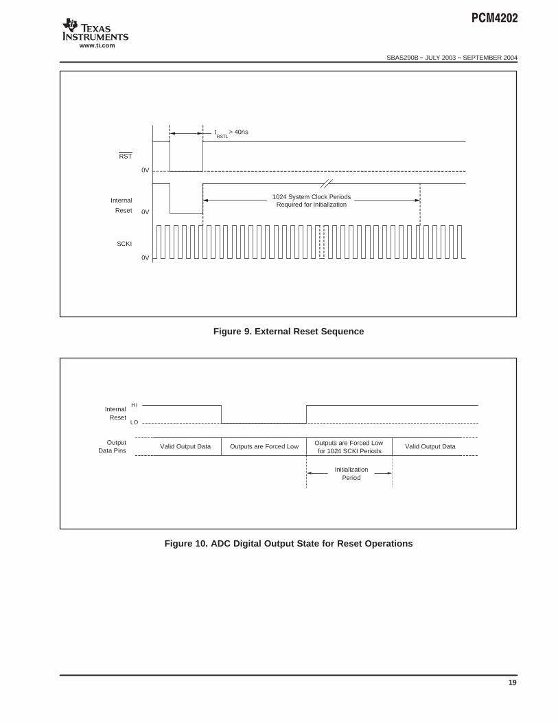
RESET OPERATION
The PCM4202 includes two reset functions: power-on andexternally controlled. This section describes the operationof each of these functions.
On power-up, the internal reset signal is forced low, forcingthe PCM4202 into a reset state. The power-on reset circuitmonitors the VDD (pin 14) and VCC (pin 22) power supplies.When the VDD supply exceeds +2.0V (±400mV) and theVCC supply exceeds +4.0V (±400mV), the internal resetsignal is forced high. The PCM4202 then waits for thesystem clock input (SCKI) to become active. Once thesystem clock has been detected, the initializationsequence begins. The initialization sequence requires1024 system clock periods for completion. During theinitialization sequence, the ADC output data pins are
forced low. Once the initialization sequence is completed,the PCM4202 output is enabled. Figure 8 shows thepower-on reset sequence timing.
The user may force a reset initialization sequence at anytime while the system clock input is active by utilizing theRST input (pin 19). The RST input is active low, andrequires a minimum low pulse width of 40ns. Thelow-to-high transition of the applied reset signal forces aninitialization sequence to begin. As in the case of thepower-on reset, the initialization sequence requires 1024system clock periods for completion. Figure 9 illustratesthe reset sequence initiated when using the RST input.
Figure 10 shows the state of the audio data outputs for thePCM4202 before, during and after the reset operations.
1024 System Clock PeriodsRequired for Initialization
System ClockIndeterminate
or Inactive
SCKI
~ 2.0V
~ 4.0V
0V
0V
0V
0V
InternalReset
VCC
VDD
Figure 8. Power-On Reset Sequence
SBAS290B − JULY 2003 − SEPTEMBER 2004
www.ti.com
19
1024 System Clock PeriodsRequired for Initialization
SCKI
Internal
Reset
0V
0V
0V
tRSTL
> 40ns
RST
Figure 9. External Reset Sequence
InternalReset
OutputData Pins
Valid Output Data Outputs are Forced Lowfor 1024 SCKI Periods
Valid Output DataOutputs are Forced Low
InitializationPeriod
HI
LO
Figure 10. ADC Digital Output State for Reset Operations
SBAS290B − JULY 2003 − SEPTEMBER 2004
www.ti.com
20
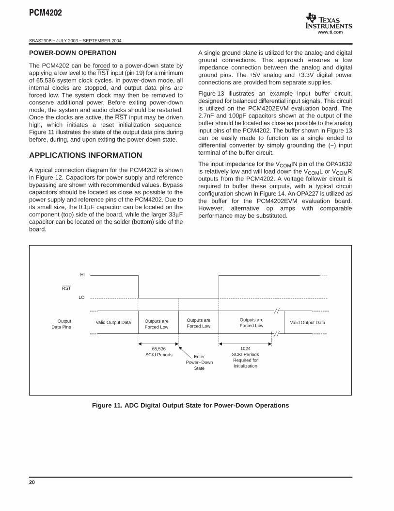
POWER-DOWN OPERATION
The PCM4202 can be forced to a power-down state byapplying a low level to the RST input (pin 19) for a minimumof 65,536 system clock cycles. In power-down mode, allinternal clocks are stopped, and output data pins areforced low. The system clock may then be removed toconserve additional power. Before exiting power-downmode, the system and audio clocks should be restarted.Once the clocks are active, the RST input may be drivenhigh, which initiates a reset initialization sequence.Figure 11 illustrates the state of the output data pins duringbefore, during, and upon exiting the power-down state.
APPLICATIONS INFORMATION
A typical connection diagram for the PCM4202 is shownin Figure 12. Capacitors for power supply and referencebypassing are shown with recommended values. Bypasscapacitors should be located as close as possible to thepower supply and reference pins of the PCM4202. Due toits small size, the 0.1µF capacitor can be located on thecomponent (top) side of the board, while the larger 33µFcapacitor can be located on the solder (bottom) side of theboard.
A single ground plane is utilized for the analog and digitalground connections. This approach ensures a lowimpedance connection between the analog and digitalground pins. The +5V analog and +3.3V digital powerconnections are provided from separate supplies.
Figure 13 illustrates an example input buffer circuit,designed for balanced differential input signals. This circuitis utilized on the PCM4202EVM evaluation board. The2.7nF and 100pF capacitors shown at the output of thebuffer should be located as close as possible to the analoginput pins of the PCM4202. The buffer shown in Figure 13can be easily made to function as a single ended todifferential converter by simply grounding the (−) inputterminal of the buffer circuit.
The input impedance for the VCOMIN pin of the OPA1632is relatively low and will load down the VCOML or VCOMRoutputs from the PCM4202. A voltage follower circuit isrequired to buffer these outputs, with a typical circuitconfiguration shown in Figure 14. An OPA227 is utilized asthe buffer for the PCM4202EVM evaluation board.However, alternative op amps with comparableperformance may be substituted.
OutputData Pins
65,536SCKI Periods
Valid Output DataOutputs areForced Low
RST
LO
HI
1024SCKI PeriodsRequired forInitialization
Valid Output Data Outputs areForced Low
Outputs areForced Low
EnterPower−Down
State
Figure 11. ADC Digital Output State for Power-Down Operations

SBAS290B − JULY 2003 − SEPTEMBER 2004
www.ti.com
21
VREFL
AGNDL
VCOML
VINL+
VINL−
FMT0
FMT1
S/M
FS0
FS1
FS2
HPFD
DGND
VDD
VREFR
AGNDR
VCOMR
VINR+
VINR−
AGND
VCC
CLIPL
CLIPR
RST
SCKI
LRCK or DSDBCK
BCK or DSDL
DATA or DSDR
1
2
3
4
5
6
7
8
9
10
11
12
13
14
28
27
26
25
24
23
22
21
20
19
18
17
16
15
PCM4202
+33µF
0.1µF
0.1µF+
33µF
+5V
Right ChannelAnalog Input
0.1µF
+
33µF
0.1µF
Left ChannelAnalog Input
Input Buffer
FromLogic, µP,
orHardwired
Connection
0.1µF
+
33µF
0.1µF
Digital AudioTransmitter or
Processor
To ClippingIndicators
To A/D or System Reset
To Audio System Clock
+3.3V
Figure 12. Typical Connection Diagram

SBAS290B − JULY 2003 − SEPTEMBER 2004
www.ti.com
22
1kΩ 40.2Ω
40.2Ω
1kΩ
270Ω
270Ω
OPA1632
1nF
1nF
1kΩDifferential
Analog Input 2.7nF
0.01µF
10µF
−15V
2
1
8EN
VOCM
100pF
To VIN−
To VIN+
FromBuffered VCOMin Figure 14.
76
3
4
5
10µF
0.01µF
+15V
(+)
+
+
(−)
100pF
0.1µF
Figure 13. Example Input Buffer Circuit
VCOML
or
VCOMR
PCM4202OPA227
or equivalent
ToBuffered VCOMin Figure 13.
0.1µF
Figure 14. Example Buffer Circuit for V COML and V COMR

SBAS290B − JULY 2003 − SEPTEMBER 2004
www.ti.com
23
COMPATIBILITY WITH THE PCM1804
Although the PCM4202 and PCM1804 are pin- andfunction-compatible, there are a few differences betweenthe two devices that the designer should be aware of.These differences are noted here for clarity.
The full-scale input of the PCM4202 is 6.0VPPdifferential, while it is 5.0VPP for the PCM1804. Thisis a result of the PCM4202 having an internal +3.0Vvoltage reference, and the PCM1804 having aninternal +2.5V voltage reference.
The PCM1804 includes +5V tolerant digital inputs.The PCM4202 does not include these because thedigital inputs are designed for interfacing to +3.3Vlogic.
The reset pin (RST) pin of the PCM4202 has aninternal pull-up resistor. For the PCM1804, this pinhas an internal pull-down resistor.
When operating in Master mode with Single Ratesampling selected, the audio serial port bit clock(BCK) is equal to 64fS for the PCM1804, while theBCK rate is equal to 128fS for the PCM4202.
The following pins on the PCM4202 and PCM1804have different names, but they perform the samefunctions.
TERMINALNUMBER
PCM4202TERMINAL NAME
PCM1804TERMINAL NAME
9 FS0 OSR0
10 FS1 OSR1
11 FS2 OSR2
12 HPFD BYPAS
20 CLIPR OVFR
21 CLIPL OVFL
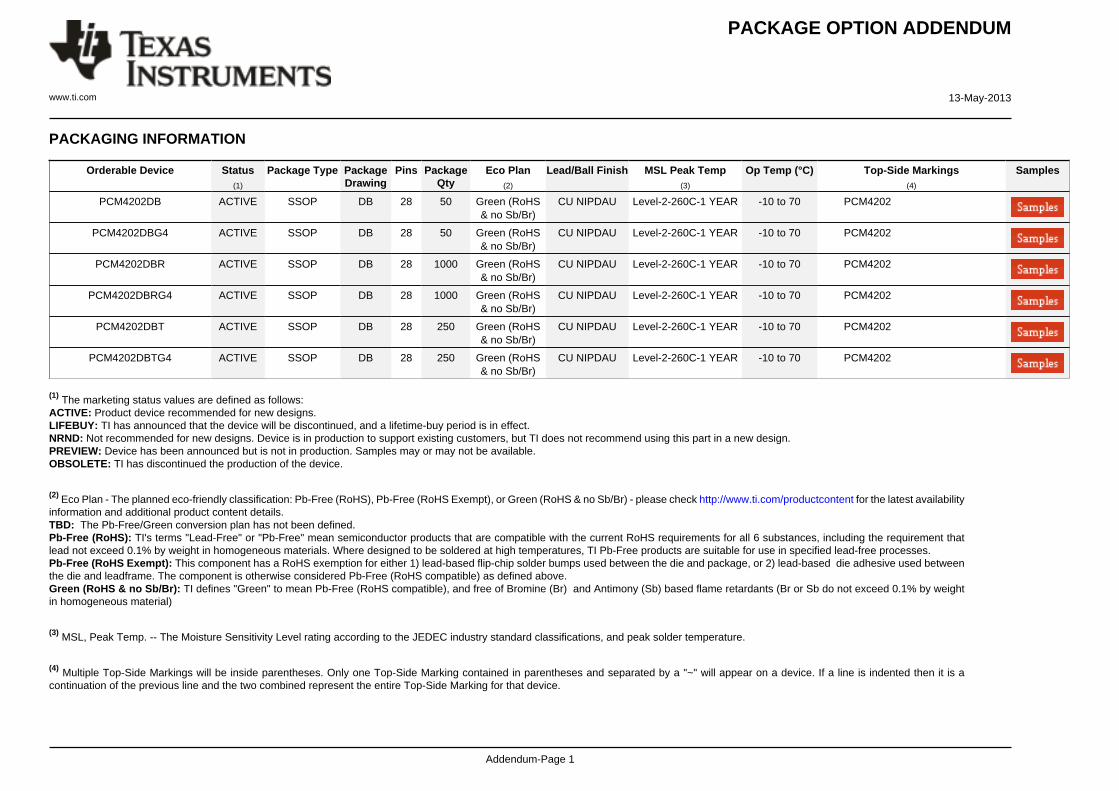
PACKAGE OPTION ADDENDUM
www.ti.com 13-May-2013
Addendum-Page 1
PACKAGING INFORMATION
Orderable Device Status(1)
Package Type PackageDrawing
Pins PackageQty
Eco Plan(2)
Lead/Ball Finish MSL Peak Temp(3)
Op Temp (°C) Top-Side Markings(4)
Samples
PCM4202DB ACTIVE SSOP DB 28 50 Green (RoHS& no Sb/Br)
CU NIPDAU Level-2-260C-1 YEAR -10 to 70 PCM4202
PCM4202DBG4 ACTIVE SSOP DB 28 50 Green (RoHS& no Sb/Br)
CU NIPDAU Level-2-260C-1 YEAR -10 to 70 PCM4202
PCM4202DBR ACTIVE SSOP DB 28 1000 Green (RoHS& no Sb/Br)
CU NIPDAU Level-2-260C-1 YEAR -10 to 70 PCM4202
PCM4202DBRG4 ACTIVE SSOP DB 28 1000 Green (RoHS& no Sb/Br)
CU NIPDAU Level-2-260C-1 YEAR -10 to 70 PCM4202
PCM4202DBT ACTIVE SSOP DB 28 250 Green (RoHS& no Sb/Br)
CU NIPDAU Level-2-260C-1 YEAR -10 to 70 PCM4202
PCM4202DBTG4 ACTIVE SSOP DB 28 250 Green (RoHS& no Sb/Br)
CU NIPDAU Level-2-260C-1 YEAR -10 to 70 PCM4202
(1) The marketing status values are defined as follows:ACTIVE: Product device recommended for new designs.LIFEBUY: TI has announced that the device will be discontinued, and a lifetime-buy period is in effect.NRND: Not recommended for new designs. Device is in production to support existing customers, but TI does not recommend using this part in a new design.PREVIEW: Device has been announced but is not in production. Samples may or may not be available.OBSOLETE: TI has discontinued the production of the device.
(2) Eco Plan - The planned eco-friendly classification: Pb-Free (RoHS), Pb-Free (RoHS Exempt), or Green (RoHS & no Sb/Br) - please check http://www.ti.com/productcontent for the latest availabilityinformation and additional product content details.TBD: The Pb-Free/Green conversion plan has not been defined.Pb-Free (RoHS): TI's terms "Lead-Free" or "Pb-Free" mean semiconductor products that are compatible with the current RoHS requirements for all 6 substances, including the requirement thatlead not exceed 0.1% by weight in homogeneous materials. Where designed to be soldered at high temperatures, TI Pb-Free products are suitable for use in specified lead-free processes.Pb-Free (RoHS Exempt): This component has a RoHS exemption for either 1) lead-based flip-chip solder bumps used between the die and package, or 2) lead-based die adhesive used betweenthe die and leadframe. The component is otherwise considered Pb-Free (RoHS compatible) as defined above.Green (RoHS & no Sb/Br): TI defines "Green" to mean Pb-Free (RoHS compatible), and free of Bromine (Br) and Antimony (Sb) based flame retardants (Br or Sb do not exceed 0.1% by weightin homogeneous material)
(3) MSL, Peak Temp. -- The Moisture Sensitivity Level rating according to the JEDEC industry standard classifications, and peak solder temperature.
(4) Multiple Top-Side Markings will be inside parentheses. Only one Top-Side Marking contained in parentheses and separated by a "~" will appear on a device. If a line is indented then it is acontinuation of the previous line and the two combined represent the entire Top-Side Marking for that device.

PACKAGE OPTION ADDENDUM
www.ti.com 13-May-2013
Addendum-Page 2
Important Information and Disclaimer:The information provided on this page represents TI's knowledge and belief as of the date that it is provided. TI bases its knowledge and belief on informationprovided by third parties, and makes no representation or warranty as to the accuracy of such information. Efforts are underway to better integrate information from third parties. TI has taken andcontinues to take reasonable steps to provide representative and accurate information but may not have conducted destructive testing or chemical analysis on incoming materials and chemicals.TI and TI suppliers consider certain information to be proprietary, and thus CAS numbers and other limited information may not be available for release.
In no event shall TI's liability arising out of such information exceed the total purchase price of the TI part(s) at issue in this document sold by TI to Customer on an annual basis.
OTHER QUALIFIED VERSIONS OF PCM4202 :
• Enhanced Product: PCM4202-EP
NOTE: Qualified Version Definitions:
• Enhanced Product - Supports Defense, Aerospace and Medical Applications
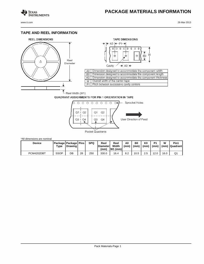
TAPE AND REEL INFORMATION
*All dimensions are nominal
Device PackageType
PackageDrawing
Pins SPQ ReelDiameter
(mm)
ReelWidth
W1 (mm)
A0(mm)
B0(mm)
K0(mm)
P1(mm)
W(mm)
Pin1Quadrant
PCM4202DBT SSOP DB 28 250 330.0 16.4 8.2 10.5 2.5 12.0 16.0 Q1
PACKAGE MATERIALS INFORMATION
www.ti.com 26-Mar-2013
Pack Materials-Page 1
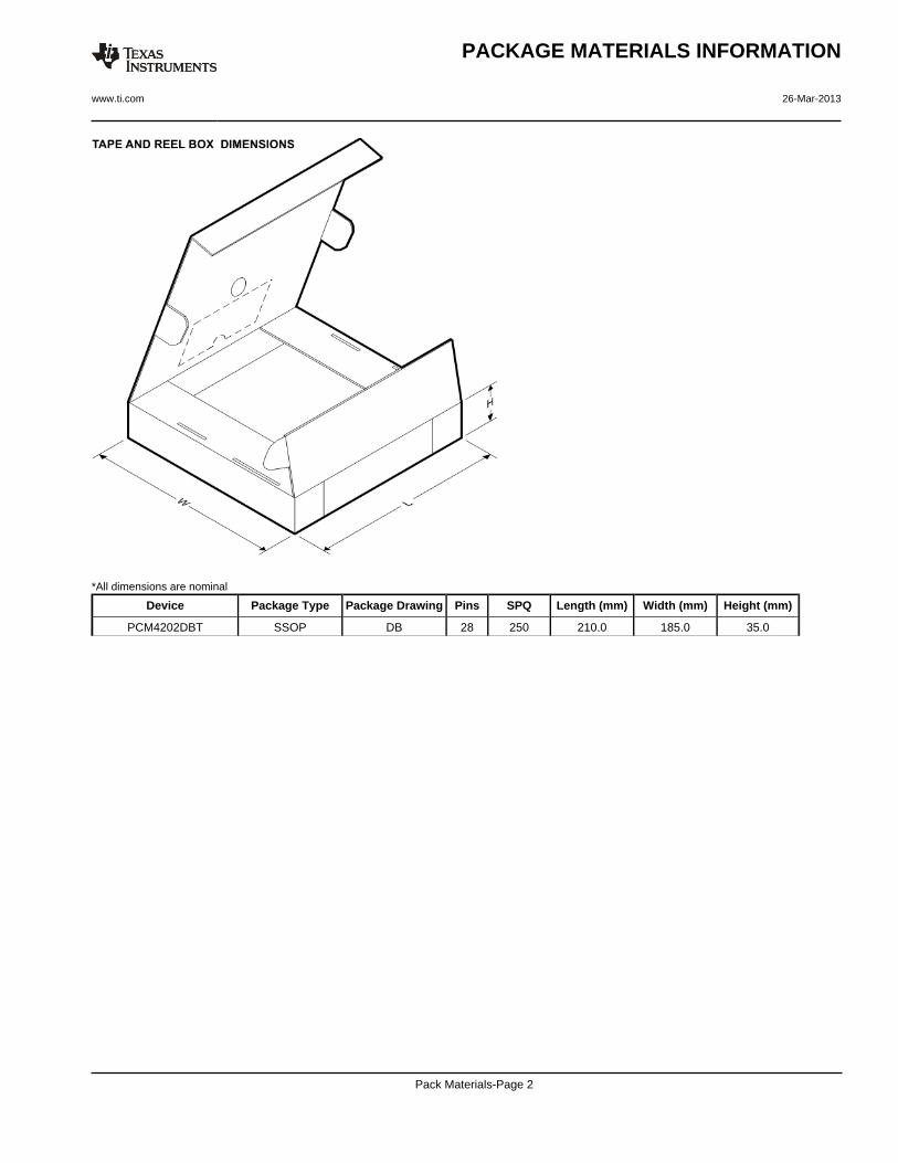
*All dimensions are nominal
Device Package Type Package Drawing Pins SPQ Length (mm) Width (mm) Height (mm)
PCM4202DBT SSOP DB 28 250 210.0 185.0 35.0
PACKAGE MATERIALS INFORMATION
www.ti.com 26-Mar-2013
Pack Materials-Page 2
www.ti.com
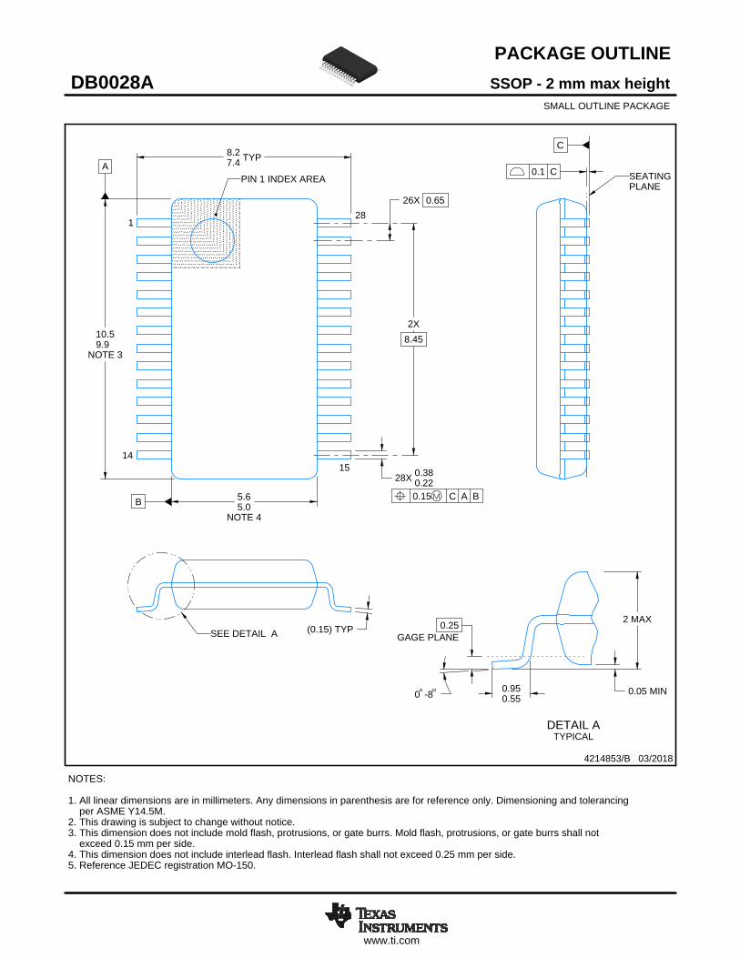
PACKAGE OUTLINE
C
26X 0.65
2X8.45
28X 0.380.22
8.27.4 TYP
SEATINGPLANE
0.05 MIN
0.25GAGE PLANE
0 -8
2 MAX
B 5.65.0
NOTE 4
A
10.59.9
NOTE 3
0.950.55
(0.15) TYP
SSOP - 2 mm max heightDB0028ASMALL OUTLINE PACKAGE
4214853/B 03/2018
1
1415
28
0.15 C A B
PIN 1 INDEX AREA
SEE DETAIL A
0.1 C
NOTES: 1. All linear dimensions are in millimeters. Any dimensions in parenthesis are for reference only. Dimensioning and tolerancing per ASME Y14.5M. 2. This drawing is subject to change without notice. 3. This dimension does not include mold flash, protrusions, or gate burrs. Mold flash, protrusions, or gate burrs shall not exceed 0.15 mm per side. 4. This dimension does not include interlead flash. Interlead flash shall not exceed 0.25 mm per side.5. Reference JEDEC registration MO-150.
A 15DETAIL ATYPICAL
SCALE 1.500
www.ti.com
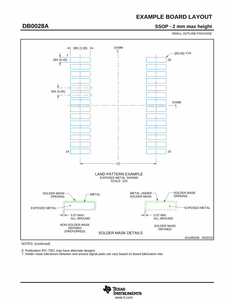
EXAMPLE BOARD LAYOUT
0.07 MAXALL AROUND
0.07 MINALL AROUND
28X (1.85)
28X (0.45)
26X (0.65)
(7)
(R0.05) TYP
SSOP - 2 mm max heightDB0028ASMALL OUTLINE PACKAGE
4214853/B 03/2018
NOTES: (continued) 6. Publication IPC-7351 may have alternate designs. 7. Solder mask tolerances between and around signal pads can vary based on board fabrication site.
LAND PATTERN EXAMPLEEXPOSED METAL SHOWN
SCALE: 10X
SYMM
SYMM
1
14 15
28
15.000
METALSOLDER MASKOPENING
METAL UNDERSOLDER MASK
SOLDER MASKOPENING
EXPOSED METALEXPOSED METAL
SOLDER MASK DETAILS
NON-SOLDER MASKDEFINED
(PREFERRED)
SOLDER MASKDEFINED

www.ti.com
EXAMPLE STENCIL DESIGN
28X (1.85)
28X (0.45)
26X (0.65)
(7)
(R0.05) TYP
SSOP - 2 mm max heightDB0028ASMALL OUTLINE PACKAGE
4214853/B 03/2018
NOTES: (continued) 8. Laser cutting apertures with trapezoidal walls and rounded corners may offer better paste release. IPC-7525 may have alternate design recommendations. 9. Board assembly site may have different recommendations for stencil design.
SOLDER PASTE EXAMPLEBASED ON 0.125 mm THICK STENCIL
SCALE: 10X
SYMM
SYMM
1
14 15
28

IMPORTANT NOTICE
Texas Instruments Incorporated (TI) reserves the right to make corrections, enhancements, improvements and other changes to itssemiconductor products and services per JESD46, latest issue, and to discontinue any product or service per JESD48, latest issue. Buyersshould obtain the latest relevant information before placing orders and should verify that such information is current and complete.TI’s published terms of sale for semiconductor products (http://www.ti.com/sc/docs/stdterms.htm) apply to the sale of packaged integratedcircuit products that TI has qualified and released to market. Additional terms may apply to the use or sale of other types of TI products andservices.Reproduction of significant portions of TI information in TI data sheets is permissible only if reproduction is without alteration and isaccompanied by all associated warranties, conditions, limitations, and notices. TI is not responsible or liable for such reproduceddocumentation. Information of third parties may be subject to additional restrictions. Resale of TI products or services with statementsdifferent from or beyond the parameters stated by TI for that product or service voids all express and any implied warranties for theassociated TI product or service and is an unfair and deceptive business practice. TI is not responsible or liable for any such statements.Buyers and others who are developing systems that incorporate TI products (collectively, “Designers”) understand and agree that Designersremain responsible for using their independent analysis, evaluation and judgment in designing their applications and that Designers havefull and exclusive responsibility to assure the safety of Designers' applications and compliance of their applications (and of all TI productsused in or for Designers’ applications) with all applicable regulations, laws and other applicable requirements. Designer represents that, withrespect to their applications, Designer has all the necessary expertise to create and implement safeguards that (1) anticipate dangerousconsequences of failures, (2) monitor failures and their consequences, and (3) lessen the likelihood of failures that might cause harm andtake appropriate actions. Designer agrees that prior to using or distributing any applications that include TI products, Designer willthoroughly test such applications and the functionality of such TI products as used in such applications.TI’s provision of technical, application or other design advice, quality characterization, reliability data or other services or information,including, but not limited to, reference designs and materials relating to evaluation modules, (collectively, “TI Resources”) are intended toassist designers who are developing applications that incorporate TI products; by downloading, accessing or using TI Resources in anyway, Designer (individually or, if Designer is acting on behalf of a company, Designer’s company) agrees to use any particular TI Resourcesolely for this purpose and subject to the terms of this Notice.TI’s provision of TI Resources does not expand or otherwise alter TI’s applicable published warranties or warranty disclaimers for TIproducts, and no additional obligations or liabilities arise from TI providing such TI Resources. TI reserves the right to make corrections,enhancements, improvements and other changes to its TI Resources. TI has not conducted any testing other than that specificallydescribed in the published documentation for a particular TI Resource.Designer is authorized to use, copy and modify any individual TI Resource only in connection with the development of applications thatinclude the TI product(s) identified in such TI Resource. NO OTHER LICENSE, EXPRESS OR IMPLIED, BY ESTOPPEL OR OTHERWISETO ANY OTHER TI INTELLECTUAL PROPERTY RIGHT, AND NO LICENSE TO ANY TECHNOLOGY OR INTELLECTUAL PROPERTYRIGHT OF TI OR ANY THIRD PARTY IS GRANTED HEREIN, including but not limited to any patent right, copyright, mask work right, orother intellectual property right relating to any combination, machine, or process in which TI products or services are used. Informationregarding or referencing third-party products or services does not constitute a license to use such products or services, or a warranty orendorsement thereof. Use of TI Resources may require a license from a third party under the patents or other intellectual property of thethird party, or a license from TI under the patents or other intellectual property of TI.TI RESOURCES ARE PROVIDED “AS IS” AND WITH ALL FAULTS. TI DISCLAIMS ALL OTHER WARRANTIES ORREPRESENTATIONS, EXPRESS OR IMPLIED, REGARDING RESOURCES OR USE THEREOF, INCLUDING BUT NOT LIMITED TOACCURACY OR COMPLETENESS, TITLE, ANY EPIDEMIC FAILURE WARRANTY AND ANY IMPLIED WARRANTIES OFMERCHANTABILITY, FITNESS FOR A PARTICULAR PURPOSE, AND NON-INFRINGEMENT OF ANY THIRD PARTY INTELLECTUALPROPERTY RIGHTS. TI SHALL NOT BE LIABLE FOR AND SHALL NOT DEFEND OR INDEMNIFY DESIGNER AGAINST ANY CLAIM,INCLUDING BUT NOT LIMITED TO ANY INFRINGEMENT CLAIM THAT RELATES TO OR IS BASED ON ANY COMBINATION OFPRODUCTS EVEN IF DESCRIBED IN TI RESOURCES OR OTHERWISE. IN NO EVENT SHALL TI BE LIABLE FOR ANY ACTUAL,DIRECT, SPECIAL, COLLATERAL, INDIRECT, PUNITIVE, INCIDENTAL, CONSEQUENTIAL OR EXEMPLARY DAMAGES INCONNECTION WITH OR ARISING OUT OF TI RESOURCES OR USE THEREOF, AND REGARDLESS OF WHETHER TI HAS BEENADVISED OF THE POSSIBILITY OF SUCH DAMAGES.Unless TI has explicitly designated an individual product as meeting the requirements of a particular industry standard (e.g., ISO/TS 16949and ISO 26262), TI is not responsible for any failure to meet such industry standard requirements.Where TI specifically promotes products as facilitating functional safety or as compliant with industry functional safety standards, suchproducts are intended to help enable customers to design and create their own applications that meet applicable functional safety standardsand requirements. Using products in an application does not by itself establish any safety features in the application. Designers mustensure compliance with safety-related requirements and standards applicable to their applications. Designer may not use any TI products inlife-critical medical equipment unless authorized officers of the parties have executed a special contract specifically governing such use.Life-critical medical equipment is medical equipment where failure of such equipment would cause serious bodily injury or death (e.g., lifesupport, pacemakers, defibrillators, heart pumps, neurostimulators, and implantables). Such equipment includes, without limitation, allmedical devices identified by the U.S. Food and Drug Administration as Class III devices and equivalent classifications outside the U.S.TI may expressly designate certain products as completing a particular qualification (e.g., Q100, Military Grade, or Enhanced Product).Designers agree that it has the necessary expertise to select the product with the appropriate qualification designation for their applicationsand that proper product selection is at Designers’ own risk. Designers are solely responsible for compliance with all legal and regulatoryrequirements in connection with such selection.Designer will fully indemnify TI and its representatives against any damages, costs, losses, and/or liabilities arising out of Designer’s non-compliance with the terms and provisions of this Notice.
Mailing Address: Texas Instruments, Post Office Box 655303, Dallas, Texas 75265Copyright © 2018, Texas Instruments Incorporated


![108dB 216kHz 32Bit CODEC with PLL - AKM · PDF file[AK4558] [AK4558] 015004500-E-03 2017/11 - 1 - 1. General Description The AK4558 is a low voltage 32bit 216kHz CODEC for high performance](https://static.fdocuments.us/doc/165x107/5a7e7d137f8b9a49588e7ad1/108db-216khz-32bit-codec-with-pll-akm-ak4558-ak4558-015004500-e-03-201711.jpg)