
Satish K Dhawan Yale University How to Deliver Oodles and Oodles of Current to HEP Detectors in High...
49
1 How to Deliver Oodles and Oodles of Current to HEP Detectors in High Radiation and Magnetic Fields? Satish K Dhawan Yale University 1 Oodle = 10,000 amps SLAC: Advanced Instrumentation Seminar February 18, 2010
-
Upload
hoangduong -
Category
Documents
-
view
220 -
download
1
Transcript of Satish K Dhawan Yale University How to Deliver Oodles and Oodles of Current to HEP Detectors in High...
1
How to Deliver Oodles and Oodles of Current to HEP Detectorsin High Radiation and Magnetic Fields?
Satish K DhawanYale University
1 Oodle
= 10,000 ampsSLAC: Advanced Instrumentation Seminar
February 18, 2010
2
Collaborators:Yale University:
Keith BakerBrookhaven National Laboratory: Hucheng Chen, James Kierstead, Francesco Lanni, David Lynn, Sergio Rescia,
Agenda
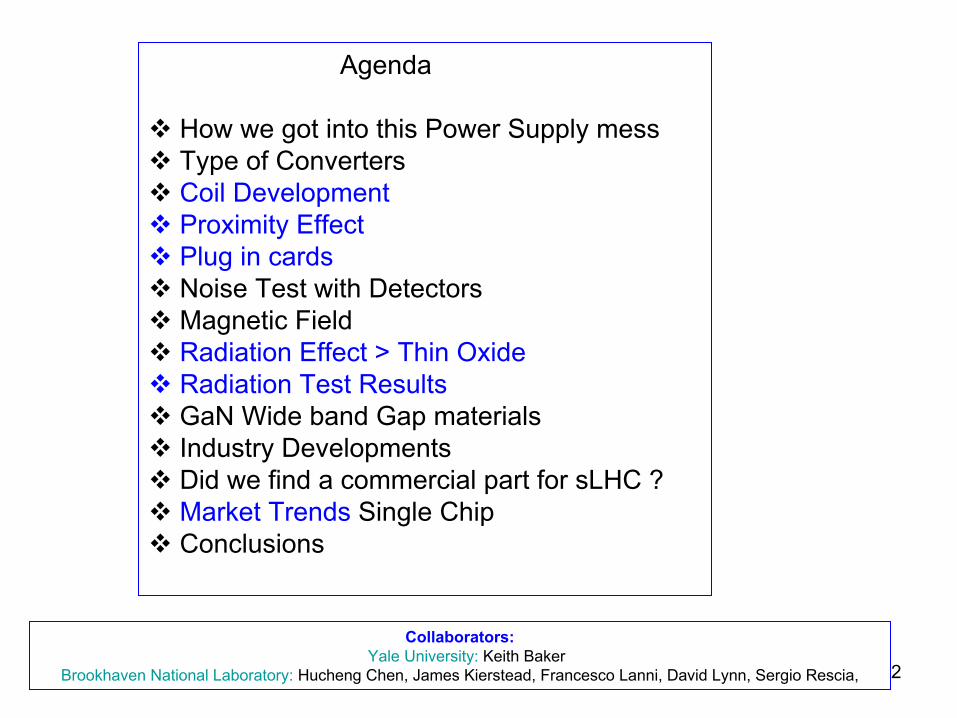
How we got into this Power Supply messType of ConvertersCoil DevelopmentProximity EffectPlug in cardsNoise Test with DetectorsMagnetic Field Radiation Effect > Thin OxideRadiation Test ResultsGaN Wide band Gap materialsIndustry DevelopmentsDid we find a commercial part for sLHC ? Market Trends Single Chip Conclusions
3
Power Supply6.3 V
SM: Super Module
2x16 mm2 (AWG 6)
50 mm2 (AWG 00)
30 m
1 to 3 mJunction Box
4 LVR Boards
64 Amps
4.3 V
2.5V64 amps160 W
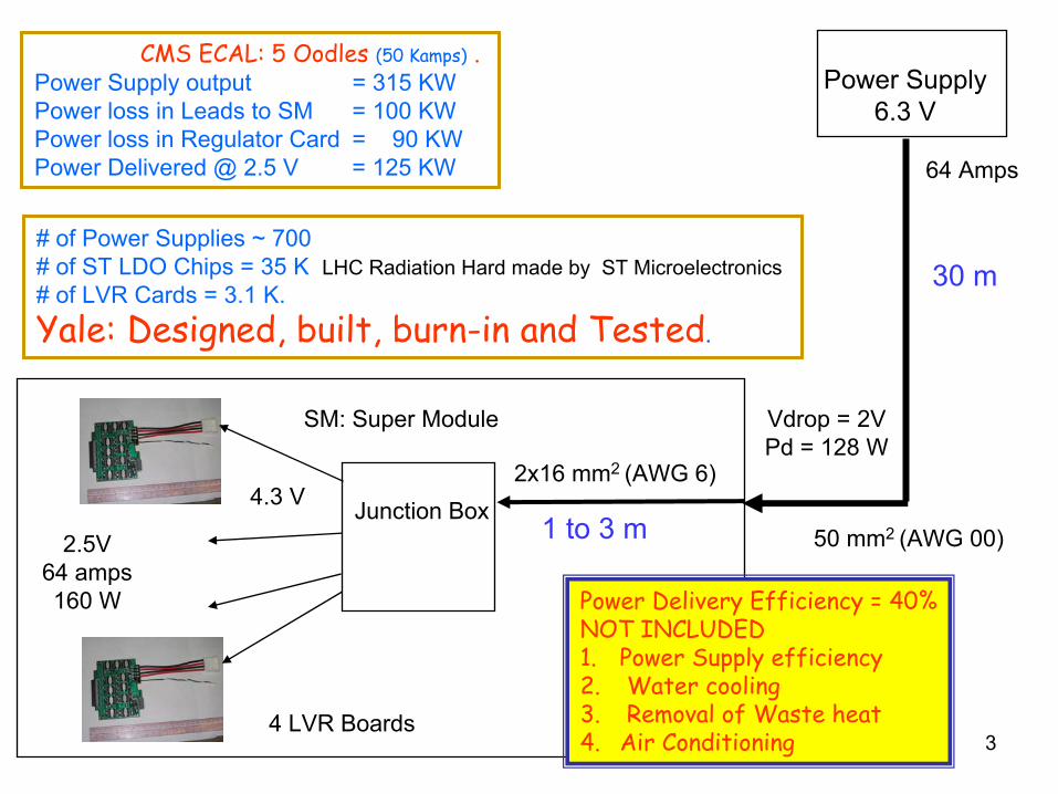
CMS ECAL: 5 Oodles (50 Kamps)
.Power Supply output = 315 KW Power loss in Leads to SM
= 100 KWPower loss in Regulator Card = 90 KWPower Delivered @ 2.5 V
= 125 KW
Vdrop
= 2VPd = 128 W
# of Power Supplies ~ 700 # of ST LDO Chips = 35 K LHC Radiation Hard made by ST Microelectronics # of LVR Cards = 3.1 K.Yale: Designed, built, burn-in and Tested.
Power Delivery Efficiency = 40%NOT INCLUDED1.
Power Supply efficiency2.
Water cooling3.
Removal of Waste heat4.
Air Conditioning

4
What can we do?•
Is there a better way to distribute power ?
•
High Radiation•
Magnetic Field 4 T
•
Load ~1 V Oodles of current•
Feed High Voltage and Convert -
like AC power
transmission
•
Commercial Technologies –
No Custom ASIC Chips
•
Learn from Semiconductor Industry•
Use Company Evaluation Boards for testing

5
IEEE JOURNAL OF SOLID-STATE CIRCUITS, VOL. 40, NO. 4, APRIL 2005
A 233-MHz 80%–87% Efficient Four-PhaseDC–DC
Converter
Utilizing Air-Core Inductors on PackagePeter Hazucha, Member, IEEE, Gerhard Schrom, Jaehong
Hahn, Bradley A. Bloechel, Associate Member, IEEE,Paul Hack, Gregory E. Dermer, Member, IEEE, Siva Narendra, Member, IEEE,
Donald Gardner, Member, IEEE, Tanay
Karnik, Senior Member, IEEE, Vivek
De, Member, IEEE, and Shekhar
Borkar, Member, IEEE
Circuit Research, Intel Laboratories, Intel Corporation, Hillsboro, OR 97124
Block diagram of a high-frequency four-phase interleaved dc–dc
converter.
Sander Mos
[[email protected]] Zero Iron Power Supply
http://www.nikhef.nl/~sanderm/zips/index.html
First Heard about Intel’s Air Coil Work in 4Q 2005 @ IDF

6
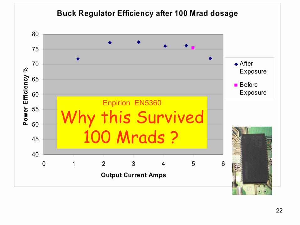
Buck Regulator Efficiency after 100 Mrad dosage
40
45
50
55
60
65
70
75
80
0 1 2 3 4 5 6
Output Current Amps
Pow
er E
ffici
ency
%
AfterExposure
BeforeExposure
Found out at Power Technology conference 0.25 µm LithographyIrradiated Stopped on St. Valentines Day 2007We reported @ TWEPP 2008 - IHP was foundry for EN5360
Enpirion EN5360With Integrated Inductor
7
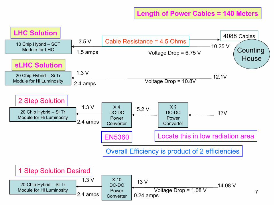
4088 Cables10 Chip Hybrid –
SCT Module for LHC Counting
House
3.5 V
20 Chip Hybrid –
Si TrModule for Hi Luminosity
Cable Resistance = 4.5 Ohms
1.5 amps
2.4 amps
X 10 DC-DCPower
Converter
20 Chip Hybrid –
Si TrModule for Hi Luminosity
1.3 V
1.3 V
2.4 amps
10.25 V
12.1V
14.08 V13 V
Voltage Drop = 6.75 V
Voltage Drop = 10.8V
0.24 ampsVoltage Drop = 1.08 V
Length of Power Cables = 140 Meters
X 4DC-DCPower
Converter
20 Chip Hybrid –
Si TrModule for Hi Luminosity
1.3 V
2.4 amps1?V
5.2 V X ?DC-DCPower
Converter
EN5360 Locate this in low radiation area
2 Step Solution
1 Step Solution Desired
sLHC Solution
LHC Solution
Overall Efficiency is product of 2 efficiencies
8
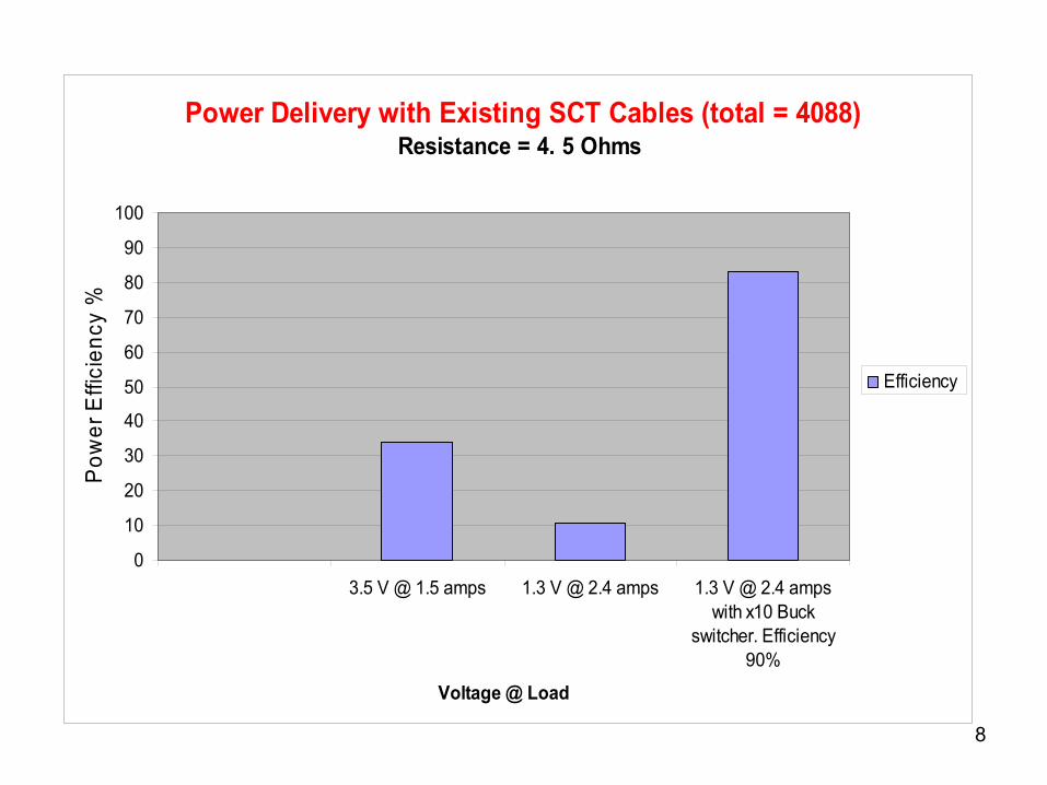
Power Delivery with Existing SCT Cables (total = 4088)Resistance = 4. 5 Ohms
0
10
20
30
40
50
60
70
80
90
100
3.5 V @ 1.5 amps 1.3 V @ 2.4 amps 1.3 V @ 2.4 ampswith x10 Buck
switcher. Efficiency90%
Voltage @ Load
Pow
er E
ffici
ency
%
Efficiency

9
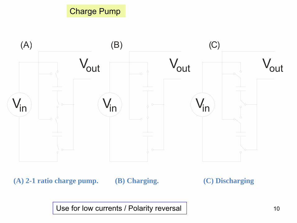
Type of High to Low Voltage Converters without transformers
Charge pumps•
Normally limited to integral fractions of input voltage•
Losses proportional to switch losses•
Can provide negative voltage
Buck Converter – Used in consumer & Industrial Electronics
•
Needs an ASIC, Inductor and Capacitors•
Cannot provide a negative voltage•
Topology allows for more flexibility in output voltage than charge pump•
Much more common use in commercial applications
9
10
V V Vin in in
V V Vout out out
(A) (B) ( )C
(A) 2-1 ratio charge pump. (B) Charging. (C) Discharging
Use for low currents / Polarity reversal
Charge Pump

11
Pulse WidthModulator
V VC
L
in outout
buck
Synchronous Buck Converter
10 V 1.1 V
100 nsec
900 nsec
Frequency = 1 MHz
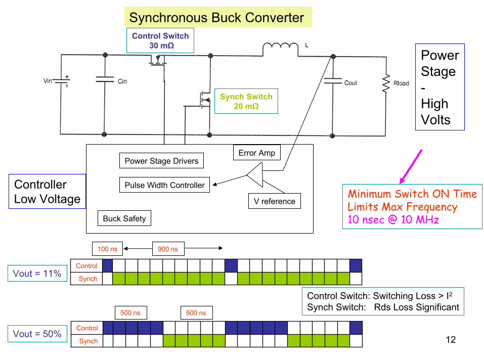
12
ControllerLow Voltage
Power Stage Drivers
V reference
Pulse Width Controller
Buck Safety
Synchronous Buck Converter
Power Stage
-High Volts
Control Switch30 mΩ
Synch Switch20 mΩ
Control Switch: Switching Loss > I2Synch Switch: Rds
Loss Significant
Error Amp
100 ns
Synch
Control
900 ns
Control
Synch
Minimum Switch ON TimeLimits Max Frequency10 nsec
@ 10 MHz
500 ns 500 ns
Vout
= 11%
Vout
= 50%
13
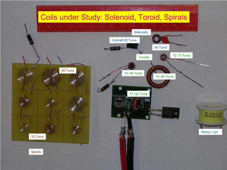
Coils under Study: Solenoid, Toroid, Spirals
Renco
1 µH
T4: 68 Turns
Coilcraft 20 Turns
40 Turns
Solenoids
Toroids
T3: 28 Turns
T2: 17 Turns
T1: 32 Turns
Spirals
20 Turns
10 Turns

14
Inductance and Resistance vs Coil Spacing
0
100
200
300
400
500
600
700
800
6 10 14 18 22Spacing (mils)
Indu
ctan
ce (n
H)
0
200
400
600
800
1000
1200
Res
ista
nce
(mΩ
)
Inductance @ 100 kHz Inductance @ 1 MHzInductance @ 5 MHz Resistance @ 100 kHzResistance @ 1 MHz Resistance @ 5 MHz
Proximity Effect
2 oz copper for coils
2 coils in series for larger L
cms
Current Distribution inNeighboring Conductors
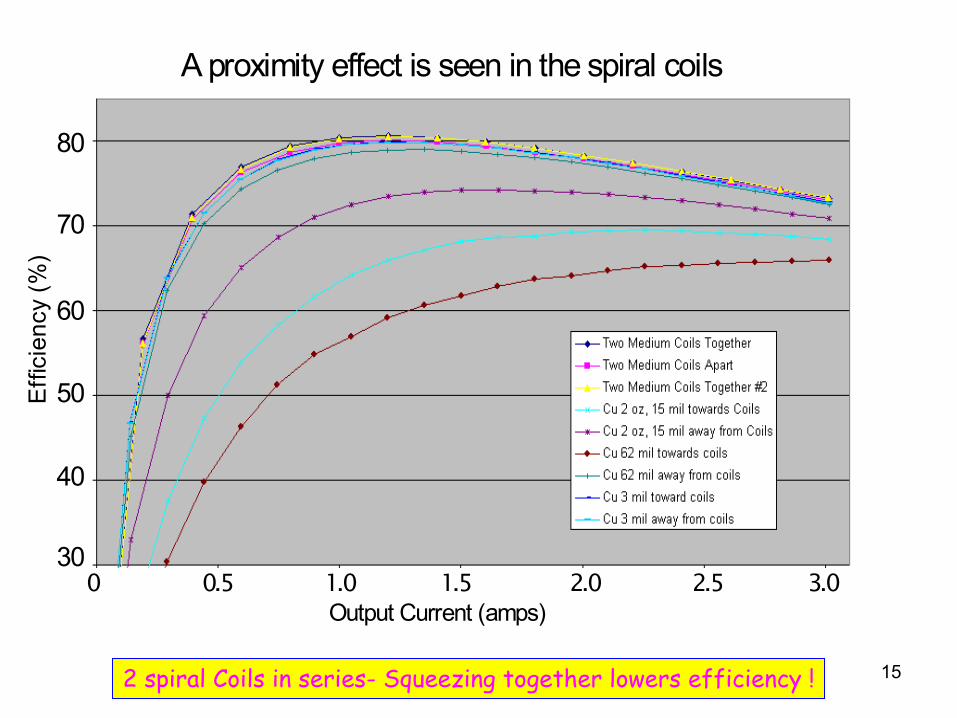
15
A proximity effect is seen in the spiral coils
30
40
50
60
70
80
Effi
cien
cy (%
)
0 0.5 2.51.51.0 2.0Output Current (amps)
3.0
2 spiral Coils in series-
Squeezing together lowers efficiency !
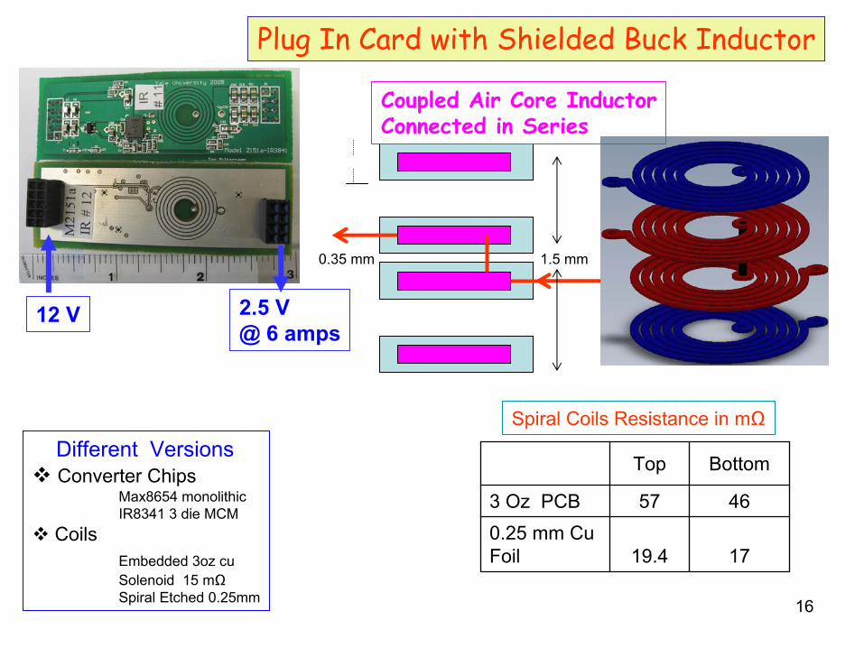
16
Coupled Air Core InductorConnected in Series
Plug In Card with Shielded Buck Inductor
0.35 mm 1.5 mm
Top Bottom
3 Oz PCB 57 460.25 mm Cu Foil 19.4 17
Spiral Coils Resistance in mΩ
12 V 2.5 V@ 6 amps
Different VersionsConverter Chips
Max8654 monolithicIR8341 3 die MCM
CoilsEmbedded 3oz cuSolenoid 15 mΩSpiral Etched 0.25mm

17
MAX8654 with embedded coils (#12), external coils (#17) or Renco Solenoid (#2) Vout=2.5 V
0
10
20
30
40
50
60
70
80
90
100
0 0.5 1 1.5 2 2.5 3 3.5 4 4.5 5Output current (amps)
Effic
ienc
y (%
)
MAX #12, Vin = 11.9 V MAX #17, Vin = 11.8 V MAX #2, Vin = 12.0 V
PCB embedded Coil
Copper Coils
Solenoid

18
aircoil #755 SP
1000
1500
2000
2500
0 200 400 600 800 1000 1200 1400 1600
channel #no
ise
ENC
IP
aircoil 13 umshielding.Aircoil parallel
aircoil 13 um shielding.Aircoil perpendicularDC-DC
RF Probe HP119441AClosed Field Probe 9KHz-
30 MHz
Scope
Shield under Test
12 µm Plastic Bag as an electrical insulator
EMI Sniffer Probes
air coil+module #755
1000
1500
2000
2500
0 200 400 600 800 1000 1200 1400 1600
channel #
nois
e EN
C
IP
AIRCOIL 65 um shield
ATLAS Si TrackerModule
12 ABCD Chips2 Sensors
Protected by plastic
Test @ Yale
Test @ RAL
RHIC
PolarimeterSilicon Sensor
With Analog Readout’Noise on Scope
Test @ BNL
Noise Tests with Silicon Sensors
Air Core Solenoid
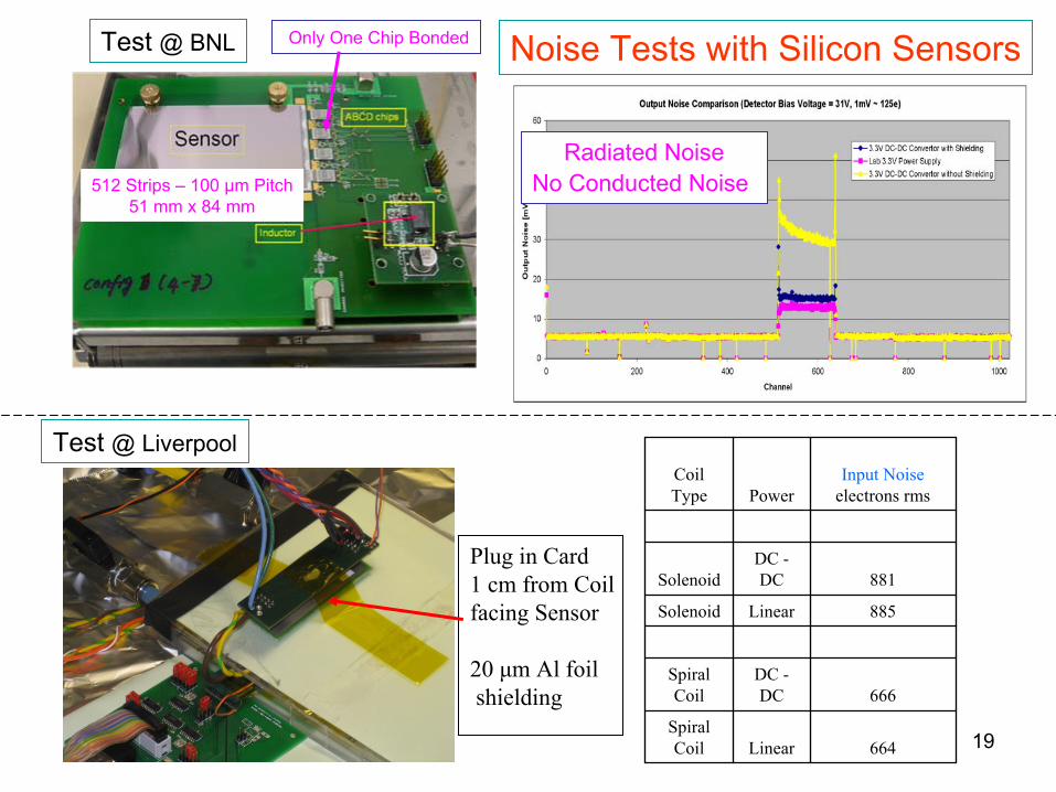
19
Plug in Card 1 cm from Coilfacing Sensor
20 μm Al foilshielding
Coil Type Power
Input Noise
electrons rms
SolenoidDC -
DC 881
Solenoid Linear 885
Spiral Coil
DC -
DC 666
Spiral Coil Linear 664
Noise Tests with Silicon SensorsTest @ BNL
Test @ Liverpool
512 Strips –
100 µm Pitch51 mm x 84 mm
Only One Chip Bonded
Radiated NoiseNo Conducted Noise
20
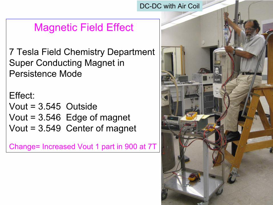
Magnetic Field Effect
7 Tesla Field Chemistry DepartmentSuper Conducting Magnet in Persistence Mode
Effect:Vout
= 3.545 Outside
Vout
= 3.546 Edge of magnetVout
= 3.549 Center of magnet
Change= Increased Vout
1 part in 900 at 7T
DC-DC with Air Coil
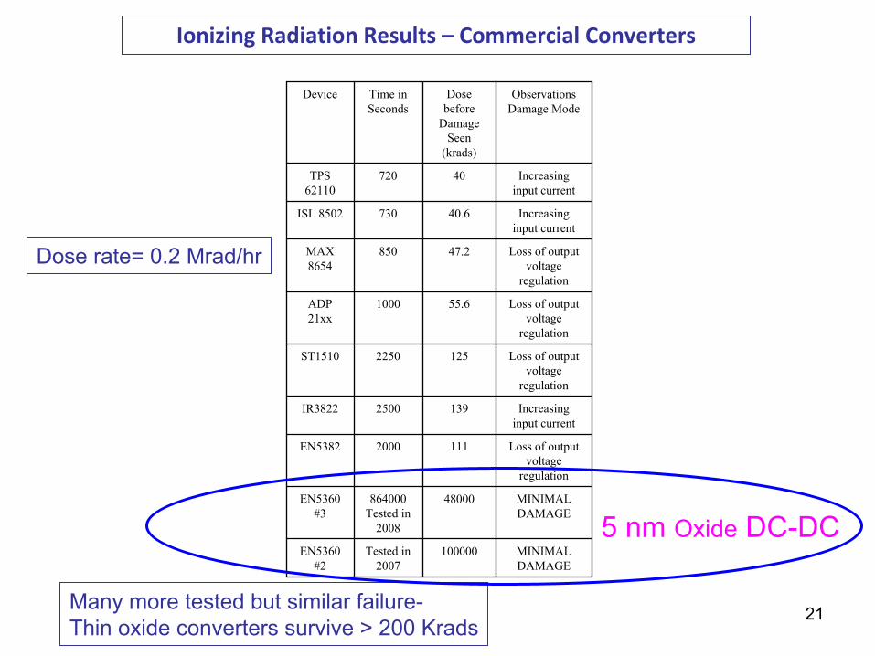
21
Device Time inSeconds
Dose before
DamageSeen
(krads)
ObservationsDamage Mode
TPS 62110
720 40 Increasing input current
ISL 8502 730 40.6 Increasing input current
MAX 8654
850 47.2 Loss of output voltage
regulation
ADP 21xx
1000 55.6 Loss of output voltage
regulation
ST1510 2250 125 Loss of output voltage
regulation
IR3822 2500 139 Increasing input current
EN5382 2000 111 Loss of output voltage
regulation
EN5360 #3
864000 Tested in
2008
48000 MINIMAL DAMAGE
EN5360 #2
Tested in 2007
100000 MINIMAL DAMAGE
Many more tested but similar failure-Thin oxide converters survive > 200 Krads
5 nm Oxide
DC-DC
Ionizing Radiation Results – Commercial Converters
Dose rate= 0.2 Mrad/hr
22
Buck Regulator Efficiency after 100 Mrad dosage
40
45
50
55
60
65
70
75
80
0 1 2 3 4 5 6
Output Current Amps
Pow
er E
ffici
ency
%
AfterExposure
BeforeExposure
Enpirion EN5360
Why this Survived100 Mrads
?
23
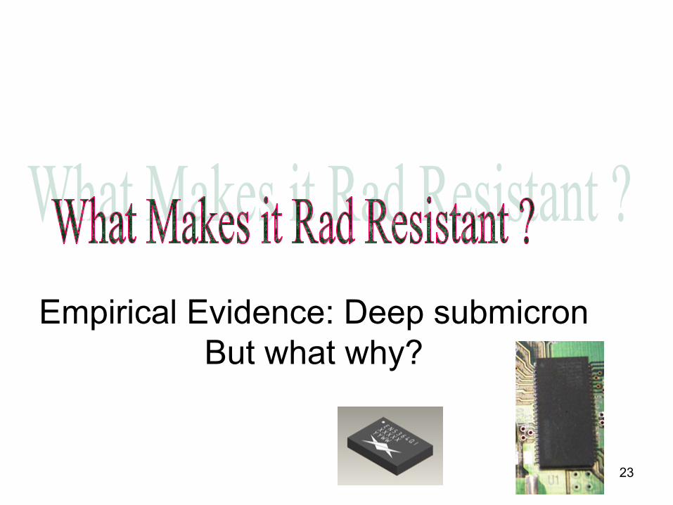
Empirical Evidence: Deep submicronBut what why?

24
We say thin Gate Oxide is anecessary
Condition

25
Sachs et. al. IEEE Trans. Nuclear Science NS-31, 1249 (1984)
Threshold Shift vs
Gate Oxide Thickness
Hole removal process by tunneling inthin-oxide MOS Structures
Book. Timothy R Oldham “Ionizing Radiation Effects in MOS Oxides”
1999 World Scientific
++ + +++ + +++ + +++ + +
++ + +
++ + +
SiSiO2
e--e--
Poly-
Si
Gate
Tunneling Region
Dosage = 150 Krads
26
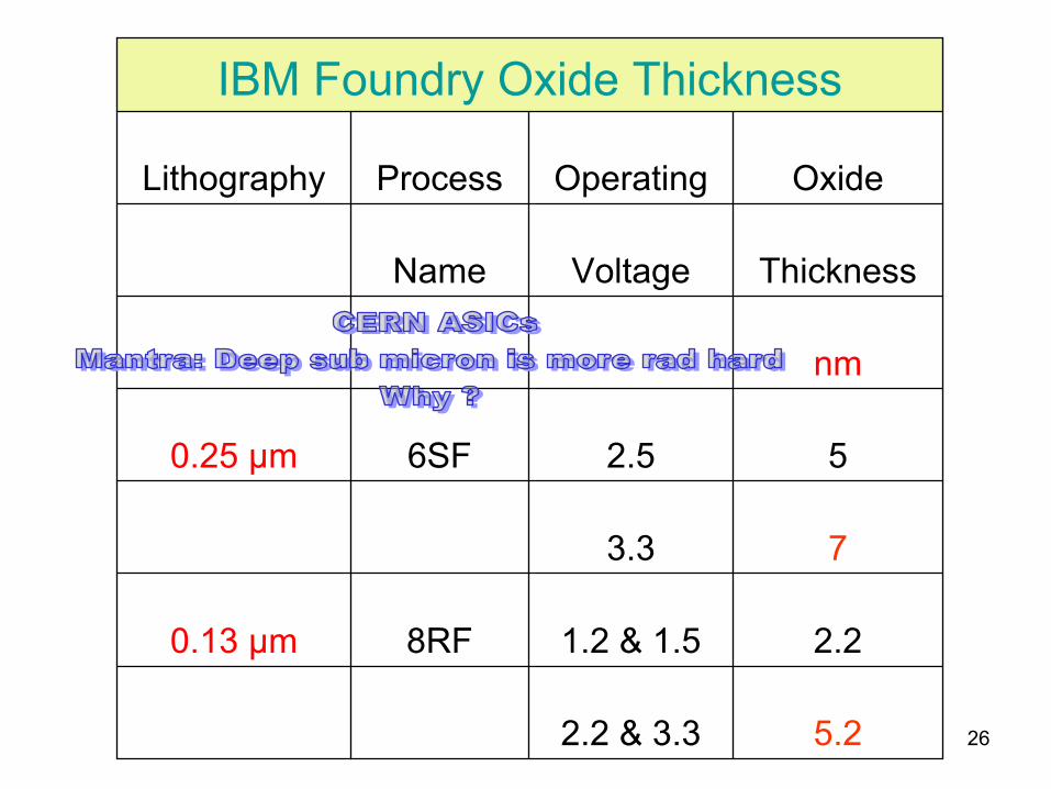
IBM Foundry Oxide Thickness
Lithography Process Operating Oxide
Name Voltage Thickness
nm
0.25 µm 6SF 2.5 5
3.3 7
0.13 µm 8RF 1.2 & 1.5 2.2
2.2 & 3.3 5.2
27
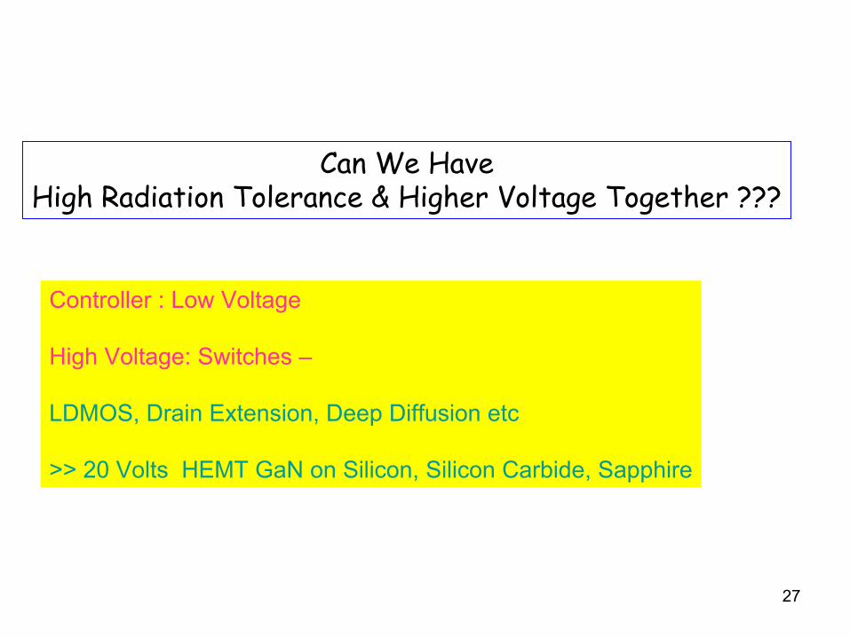
Controller : Low Voltage
High Voltage: Switches –
LDMOS, Drain Extension, Deep Diffusion etc
>> 20 Volts HEMT GaN on Silicon, Silicon Carbide, Sapphire
Can We HaveHigh Radiation Tolerance & Higher Voltage Together ???
28
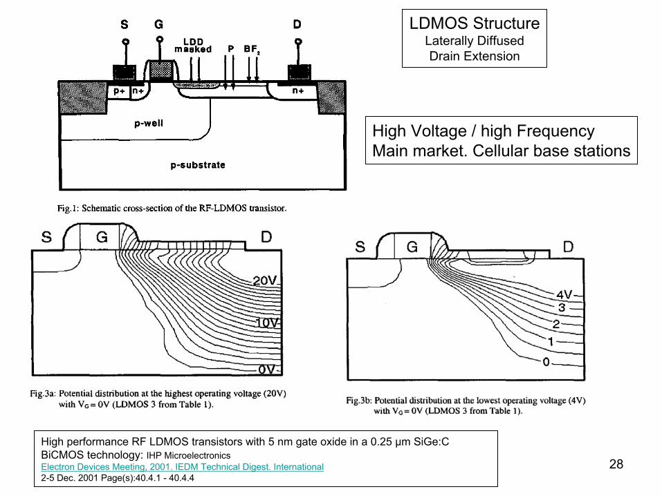
High performance RF LDMOS transistors with 5 nm gate oxide in a 0.25 μm SiGe:C
BiCMOS
technology: IHP MicroelectronicsElectron Devices Meeting, 2001. IEDM Technical Digest. International
2-5 Dec. 2001 Page(s):40.4.1 -
40.4.4
LDMOS StructureLaterally DiffusedDrain Extension
High Voltage / high FrequencyMain market. Cellular base stations

29R. Sorge et al , IHP Proceedings of SIRF 2008 ConferenceHigh Voltage Complementary Epi
Free LDMOS Module with 70 VPLDMOS for a 0.25 μm
SiGe:C
BiCMOS
Platform
30
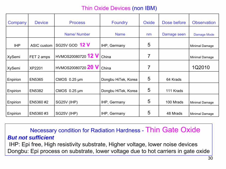
Company Device Process Foundry Oxide Dose before Observation
Name/ Number Name nm Damage seen Damage Mode
IHP ASIC custom SG25V GOD 12 V IHP, Germany 5 Minimal Damage
XySemi FET 2 amps HVMOS20080720 12 V China 7 Minimal Damage
XySemi XP2201 HVMOS20080720 20 V China 7 1Q2010
Enpirion EN5365 CMOS 0.25 µm Dongbu
HiTek, Korea 5 64 Krads
Enpirion EN5382 CMOS 0.25 µm Dongbu
HiTek, Korea 5 111 Krads
Enpirion EN5360 #2 SG25V (IHP) IHP, Germany 5 100 Mrads Minimal Damage
Enpirion EN5360 #3 SG25V (IHP) IHP, Germany 5 48 Mrads Minimal Damage
Thin Oxide Devices (non IBM)
Necessary condition for Radiation Hardness -
Thin Gate OxideBut not sufficientIHP: Epi
free, High resistivity substrate, Higher voltage, lower noise devicesDongbu: Epi
process on substrate, lower voltage due to hot carriers in gate
oxide

31
XY Semi (VD = 12V)2 Amp FET‐ HVMOS20080720 Process
00.020.040.060.080.1
0.12
0 0.5 1 1.5
Vg (Volts)
Id (A
mps)I
0 rad
1 Mrad
5.4 Mrad
33 Mrad
52 Mrad
IHP PMOS TransistorVG versus ID at selected Gamma Doses
0
0.2
0.4
0.6
0.8
1
0 0.5 1 1.5 2 2.5VG (Volts)
I D (m
A)
Pre-Irradiation
13 Mrad
22 Mrad
35 Mrad
53 Mrad
IHP NMOS TransistorVG versus ID at Selected Gamma Doses
0
0.5
1
1.5
2
2.5
0 0.5 1 1.5 2 2.5VG (Volts)
I D (m
A)
Pre-irradiation
13 Mrad
22 Mrad
35 Mrad
32
Replacement for LHC4913:LHC Radiation Hard LDOMade by ST Microelectronics
Use with Ferrite Coil
Engineering Samples1Q2010
Non-
Synchronous
33
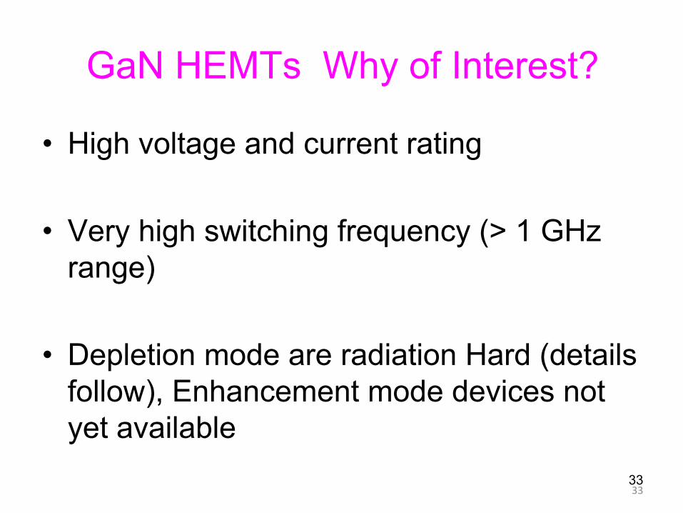
GaN
HEMTs
Why of Interest?
•
High voltage and current rating
•
Very high switching frequency (> 1 GHz range)
•
Depletion mode are radiation Hard (details follow), Enhancement mode devices not yet available
33
34
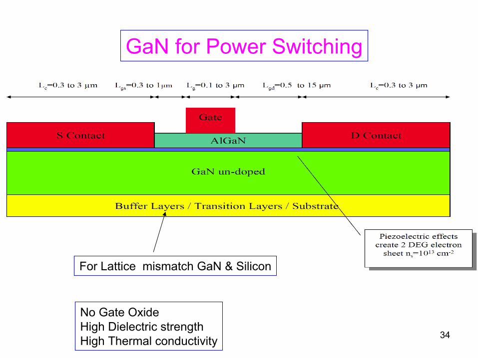
GaN for Power Switching
For Lattice mismatch GaN
& Silicon
No Gate OxideHigh Dielectric strengthHigh Thermal conductivity

35
Depletion ModeNormally ON
Enhancement ModeNormally OFF
Gate Oxide ?

36
RF GaN
20 Volts & 0.1 amp8 pieces: Nitronex NPT 25015: GaN on Silicon
Done Gamma, Proton & Neutrons65 volts Oct 2009
2 pieces: CREE CGH40010F: GaN on siC
6 pieces: Eudyna EGNB010MK: GaN on siCDone Neutrons
Switch GaNInternational Rectifier GaN on Silicon
Under NDA
Gamma: @ BNLProtons: @ LansceNeutrons: @ U of Mass Lowell
Gallium Nitride Devices under Tests
Plan to Expose same device toGamma, Protons & NeutronsOnline Monitoring
37
Source
FET
Satish Dhawan, Yale University
Pulse Generator0.1 –
2 MHz50 % Duty Cycle
July 28. 2009 FET Setup for Proton Radiation Exposure
.
~ 0.070 Amps Power SupplyV out = 20 Volts
Drain
Gate
100
0 to -
5 V
Powered FET
DMMDC mV
330 2 Watts 1 Ω
GND
50 ΩTerminator
2 ShortedFETs
Rad vs wo BiasG
DS
Pomona Box
Reading = ~ 0.035 Amps@ 50% Duty Cycle
30 m
Bias during RadiationMax operating V & I Limit Power by duty cycle
38
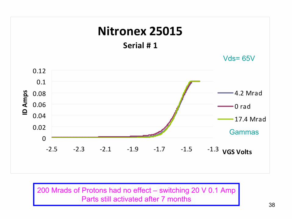
Nitronex 25015 Serial # 1
0
0.02
0.04
0.06
0.08
0.1
0.12
‐2.5 ‐2.3 ‐2.1 ‐1.9 ‐1.7 ‐1.5 ‐1.3 VGS Volts
ID Amps 4.2 Mrad
0 rad
17.4 Mrad
200 Mrads of Protons had no effect –
switching 20 V 0.1 AmpParts still activated after 7 months
Vds= 65V
Gammas

39
Proton TestProton Fluence =1 x 10¹⁵p/cm2 over a period of about 24 hours. Biased = 65 volts switching @ 1MHzAverage current = 65 mA limited by Load resistor . No change in
current.
Our next IEEE TNS Paper shall summarize
work to date
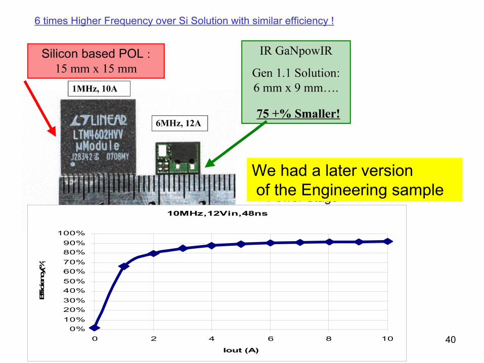
40
10MHz,12Vin,48ns
0%10%20%30%40%50%60%70%80%90%
100%
0 2 4 6 8 10
Iout (A)
Effic
ienc
y(%)
We had a later versionof the Engineering sample
41
Fuji FB6831J LT4602
MAX8654 Monolithic IR8341 MCM
EN5382 with 30AWG
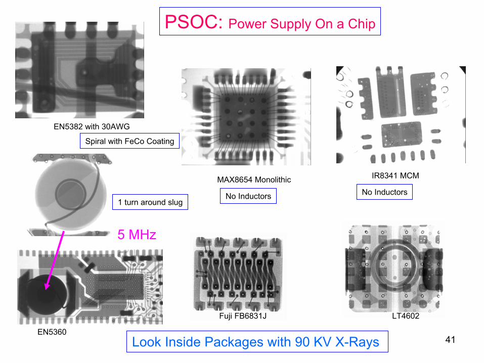
EN5360Look Inside Packages with 90 KV X-Rays
No Inductors No Inductors1 turn around slug
Spiral with FeCo
Coating
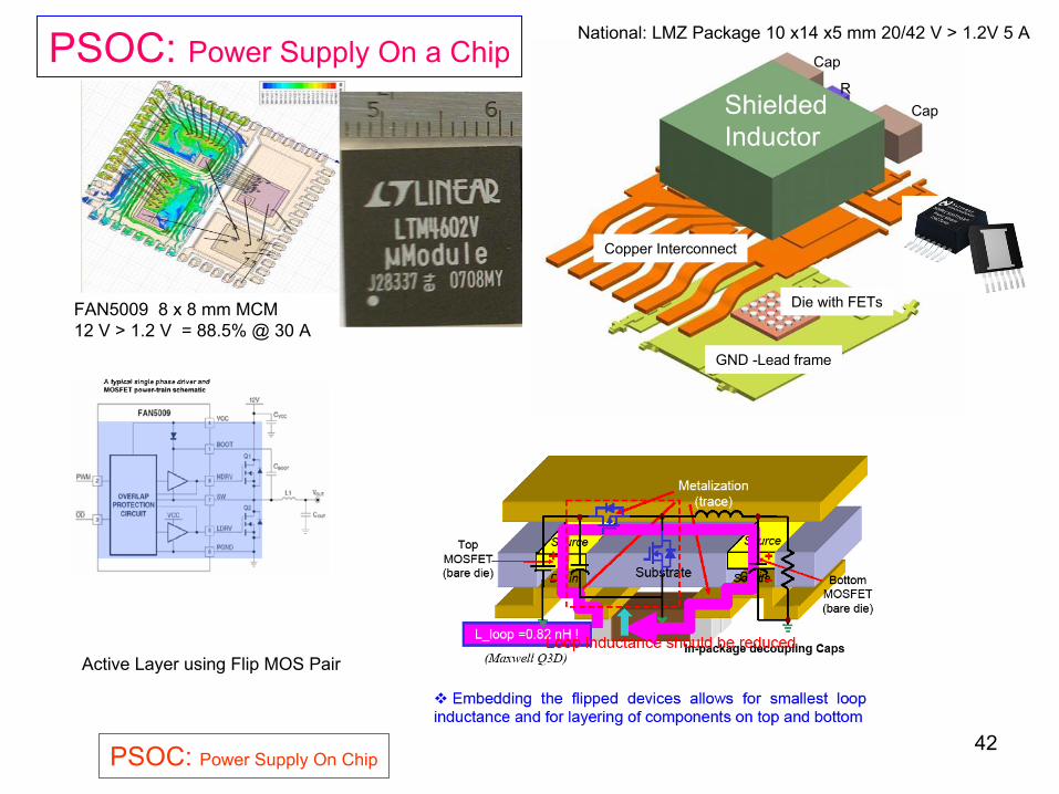
PSOC: Power Supply On a Chip
5 MHz
42
FAN5009 8 x 8 mm MCM12 V > 1.2 V = 88.5% @ 30 A
PSOC: Power Supply On Chip
National: LMZ Package 10 x14 x5 mm 20/42 V > 1.2V 5 A
ShieldedInductor
Cap
RCap
Copper Interconnect
GND -Lead frame
Die with FETs
PSOC: Power Supply On a Chip
Active Layer using Flip MOS Pair

43
Server Power System Distribution from IBM
PSMA: Road MapsPower Supply Manufacturer Association
Yale University is member
International Workshop onPower Supply On Chip
Sept 22nd -
24, 2008
Cork, Ireland
What is happening outside HEP ?
44
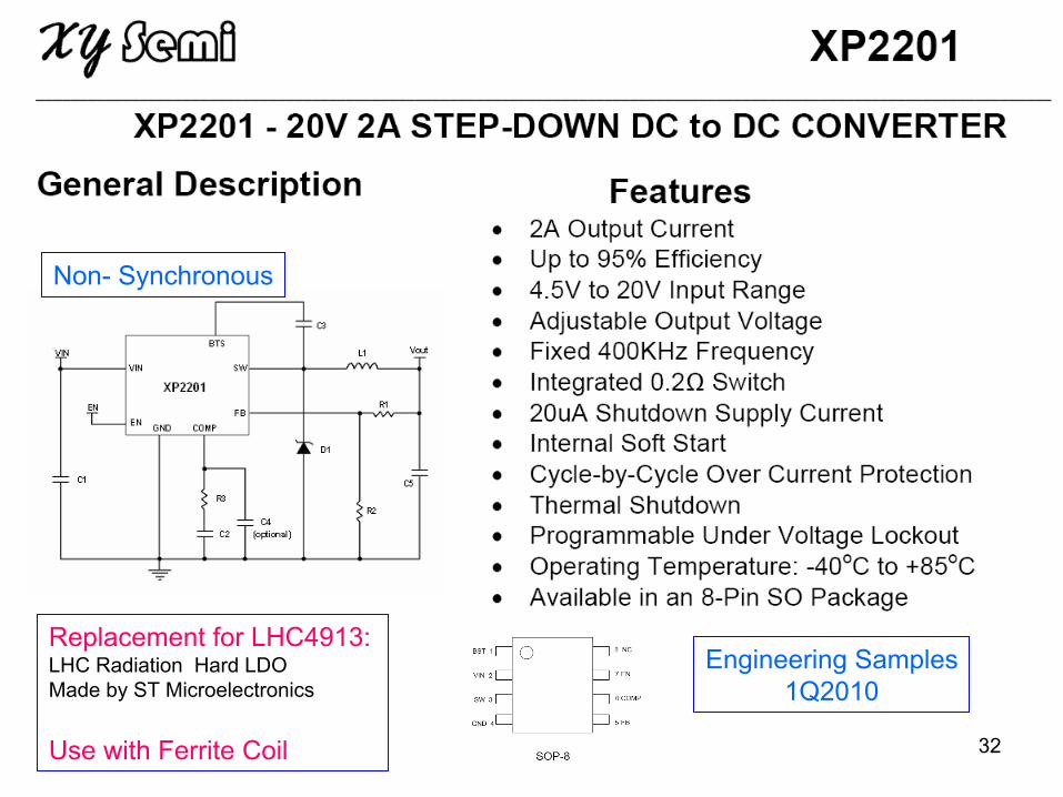
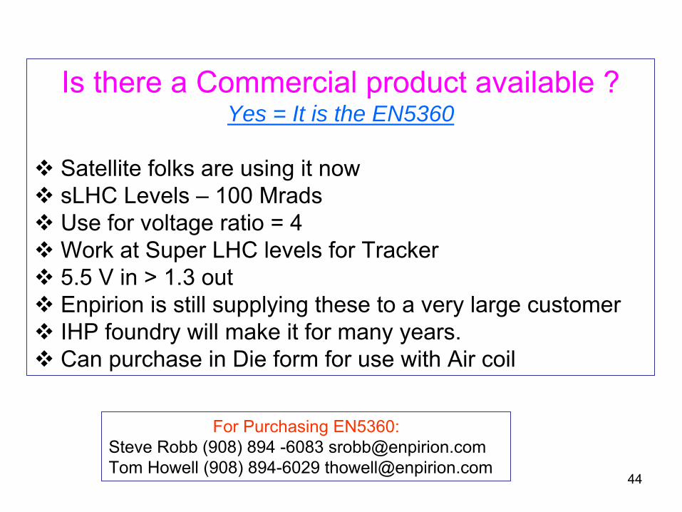
For Purchasing EN5360:Steve Robb (908) 894 -6083 [email protected] Howell (908) 894-6029 [email protected]
Is there a Commercial product available ? Yes = It is the EN5360
Satellite folks are using it nowsLHC Levels – 100 MradsUse for voltage ratio = 4Work at Super LHC levels for Tracker5.5 V in > 1.3 outEnpirion is still supplying these to a very large customerIHP foundry will make it for many years.Can purchase in Die form for use with Air coil

45
Some Random Remarks•
Learned from commercial devices, companies & power
conferences• Can get high radiation tolerance & higher voltage
simultaneously
• High frequency > smaller air coil > less material• Goal: ~20 MHz buck, MEM on Chip size 9 mm x 9mm• Power SOC: MEMs
air core inductor on chip
• Will study feasibility of 48 / 300V converters • Irradiations:
o Important to run @ max operating V & I. o Limit power dissipation by switching duty cycleo Use online monitoring during irradiation for faster results
• Yale Plug Cards can be loaned
for evaluation• Collaborators are Welcome
46
Conclusions•
The power distribution needs of HEP detectors require new solutions/technologies to meet power and environmental requirements.
•
DC/DC (Buck) Converters are potential solutions for these needs.
•
The environment requires that these converters operate in high radiation environments and high magnetic fields at high switching frequencies in a small size/mass package.
•
Target technologies for the switches are radiation hard GaN and 0.25 μm LDMOS. High frequency controllers driving small sized nonmagnetic/air core inductors are also required.
•
Many of these components have been tested and now need integration to produce a working prototype. This is the next step in our R&D program.

47
Top of the World is Cool but lonely !
Working on Power Supply Is not Glamorous
More Details:
www.Yale.edu/FASTCAMAC
click on DC-DC
48
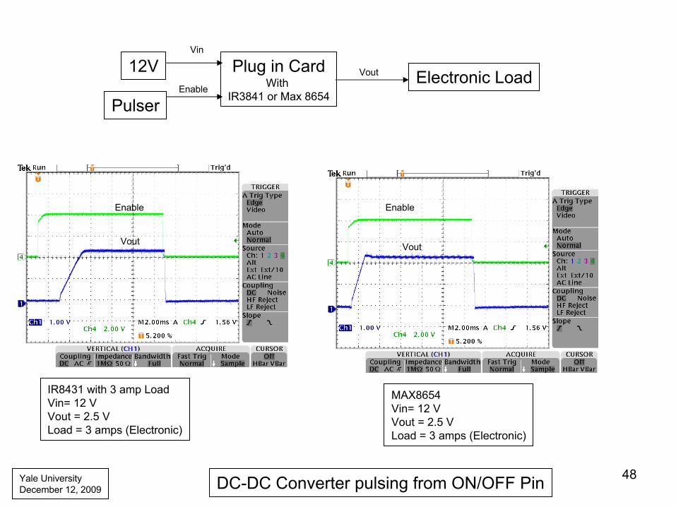
IR8431 with 3 amp LoadVin= 12 VVout
= 2.5 VLoad = 3 amps (Electronic)
MAX8654Vin= 12 VVout
= 2.5 VLoad = 3 amps (Electronic)
DC-DC Converter pulsing from ON/OFF PinYale UniversityDecember 12, 2009
Plug in CardWith
IR3841 or Max 8654
12V
PulserEnable
Vin
Vout Electronic Load
Enable Enable
Vout Vout
49
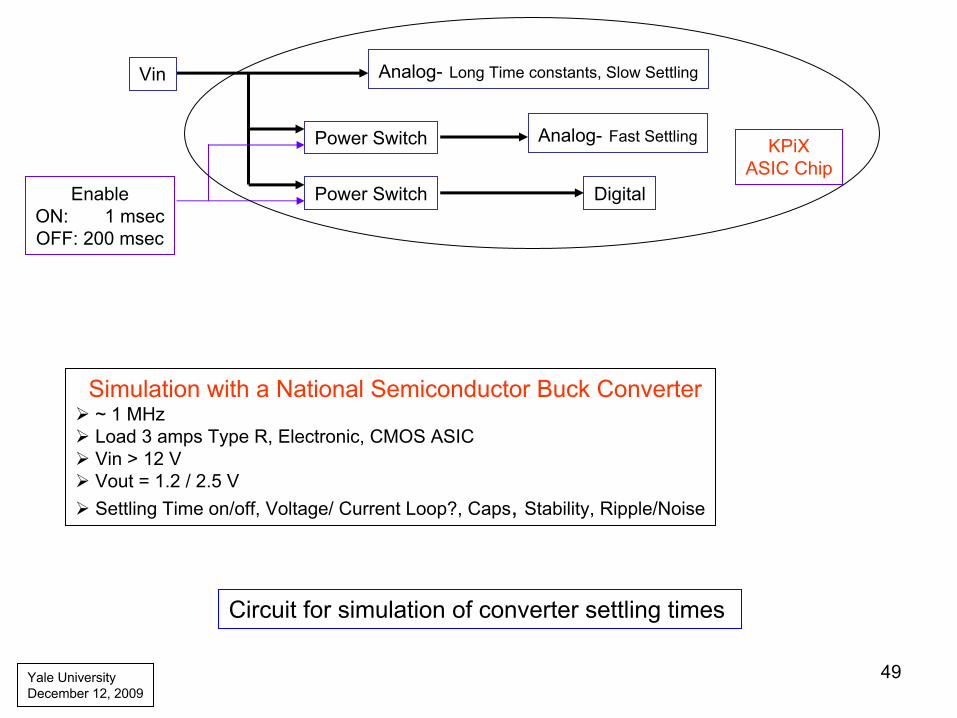
Simulation with a National Semiconductor Buck
Converter~ 1 MHzLoad 3 amps Type R, Electronic, CMOS ASIC Vin > 12 VVout = 1.2 / 2.5 VSettling Time on/off, Voltage/ Current Loop?, Caps, Stability, Ripple/Noise
Analog-
Long Time constants, Slow Settling
Analog-
Fast Settling
DigitalPower Switch
Power Switch
Vin
EnableON: 1 msecOFF: 200 msec
KPiXASIC Chip
Yale UniversityDecember 12, 2009
Circuit for simulation of converter settling times