
SATA IP Transport & Link Layer Core Core Facts Design ... · The SATA IP Core evaluation on ML605...
10
April 26, 2010 Product Specification Rev1.0 April 26, 2010 SATA IP Transport & Link Layer Core Design Gateway Co.,Ltd 54 BB Building 13 th Fl., Room No.1302 Sukhumvit 21 Rd. (Asoke), Klongtoey-Nua, Wattana, Bangkok 10110 Phone: (+66) 02-261-2277 Fax: (+66) 02-261-2290 E-mail: [email protected] URL: www.design-gateway.com Features • Compliant with the Serial ATA specification revision 2.6 • Support both of SATA Host and SATA Device (Applicable to SATA Peripheral development) • Simple transaction interface with Host processor or DMA Engine • 32-bit internal data path • 4KB FIFO implemented by BlockRAM in transmit and receive paths • Support SATA II Speed • Low frequency operation - IP Core clock 75.0MHz and PHY clock 150MHz for SATA-II • CONT primitive support for continue primitive suppression to reduce EMI • Support 20bit width PHY implemented by Virtex-6 GTX • Host Raid Reference design available on ML605 (with 8-Ch PCIe2SATA adapter board) Table 1: Example Implementation Statistics Family Example Device Fmax (MHz) Slice FFs Slice LUTs Slices 1 IOB 2 BUFGCTRL RAMB18E1 MMCM GTX Design Tools Virtex-6 LXT XC6VLX240T-1FF1156 285 1065 1274 488 119 3 2 1 1 ISE ® 11.5 Notes: 1) Actual slice count dependent on percentage of unrelated logic – see Mapping Report File for details 2) Assuming all core I/Os and clocks are routed off-chip 3) BUFG, MMCM, and GTX resource is not used in SATA IP core, but they are used in SATA PHY design. Core Facts Provided with Core Documentation User Guide, Design Guide Design File Formats NGC Netlist Constraints Files User constraint file Verification Test Bench, Simulation Library Instantiation Templates VHDL Reference Designs & Application Notes EDK Project, See Reference Design Manual Additional Items Demo on ML605 Simulation Tool Used Modelsim SE 6.5d Support Support Provided by Design Gateway Co., Ltd.
Transcript of SATA IP Transport & Link Layer Core Core Facts Design ... · The SATA IP Core evaluation on ML605...

April 26, 2010 Product Specification Rev1.0
April 26, 2010
SATA IP Transport & Link Layer Core
Design Gateway Co.,Ltd 54 BB Building 13
th Fl., Room No.1302 Sukhumvit
21 Rd. (Asoke), Klongtoey-Nua, Wattana, Bangkok 10110 Phone: (+66) 02-261-2277 Fax: (+66) 02-261-2290 E-mail: [email protected] URL: www.design-gateway.com
Features
• Compliant with the Serial ATA specification
revision 2.6
• Support both of SATA Host and SATA Device
(Applicable to SATA Peripheral development)
• Simple transaction interface with Host
processor or DMA Engine
• 32-bit internal data path
• 4KB FIFO implemented by BlockRAM in transmit and receive paths
• Support SATA II Speed
• Low frequency operation
- IP Core clock 75.0MHz and PHY clock 150MHz for SATA-II
• CONT primitive support for continue primitive suppression to reduce EMI
• Support 20bit width PHY implemented by Virtex-6 GTX
• Host Raid Reference design available on ML605 (with 8-Ch PCIe2SATA adapter board)
Table 1: Example Implementation Statistics
Family Example Device
Fmax
(MHz)
Slice
FFs
Slice
LUTs Slices
1 IOB2 BUFGCTRL RAMB18E1 MMCM GTX
Design
Tools
Virtex-6 LXT XC6VLX240T-1FF1156 285 1065 1274 488 119 3 2 1 1 ISE® 11.5
Notes:
1) Actual slice count dependent on percentage of unrelated logic – see Mapping Report File for details
2) Assuming all core I/Os and clocks are routed off-chip
3) BUFG, MMCM, and GTX resource is not used in SATA IP core, but they are used in SATA PHY design.
Core Facts
Provided with Core
Documentation User Guide, Design Guide
Design File Formats NGC Netlist
Constraints Files User constraint file
Verification Test Bench, Simulation Library
Instantiation Templates VHDL
Reference Designs &
Application Notes
EDK Project,
See Reference Design Manual
Additional Items Demo on ML605
Simulation Tool Used
Modelsim SE 6.5d
Support
Support Provided by Design Gateway Co., Ltd.
SATA IP Transport & Link Layer Core
2 April 26, 2010
FIS I/F
Scrambler
Descrambler
CRC
Control
TX Packet
RX Packet
SATA IP CoreHost
Processor
OOB Control
TX
FIFO
RX
FIFO
PHY LayerLink LayerTransport Layer
20 bit P
HY I/F
GTX on
Virtex-6 LXT
OR
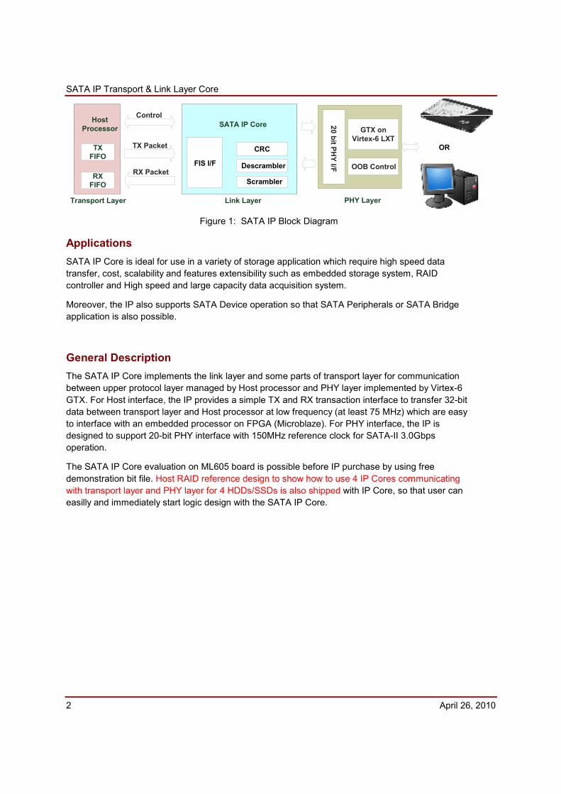
Figure 1: SATA IP Block Diagram
Applications
SATA IP Core is ideal for use in a variety of storage application which require high speed data
transfer, cost, scalability and features extensibility such as embedded storage system, RAID
controller and High speed and large capacity data acquisition system.
Moreover, the IP also supports SATA Device operation so that SATA Peripherals or SATA Bridge
application is also possible.
General Description
The SATA IP Core implements the link layer and some parts of transport layer for communication
between upper protocol layer managed by Host processor and PHY layer implemented by Virtex-6
GTX. For Host interface, the IP provides a simple TX and RX transaction interface to transfer 32-bit
data between transport layer and Host processor at low frequency (at least 75 MHz) which are easy
to interface with an embedded processor on FPGA (Microblaze). For PHY interface, the IP is
designed to support 20-bit PHY interface with 150MHz reference clock for SATA-II 3.0Gbps
operation.
The SATA IP Core evaluation on ML605 board is possible before IP purchase by using free
demonstration bit file. Host RAID reference design to show how to use 4 IP Cores communicating
with transport layer and PHY layer for 4 HDDs/SSDs is also shipped with IP Core, so that user can
easilly and immediately start logic design with the SATA IP Core.

Design Gateway Co., Ltd.
April 26, 2010 3
Functional Description
The SATA IP Core is designed to operate under control of a system controller to transfer SATA FIS
packet from/to system memory consisted of the following components.
Link Layer
The Link layer transmits and receives frames, transmits primitives based on control signals from the
transport layer, and receives primitives from SATA PHY which are converted to control signals to the
transport layer.
• CRC
The CRC of a frame is a Dword (32-bit) field that shall follow the last Dword of the
contents of a FIS and precede EOF primitive.
• Scramble
The content of a frame is scrambled before transmission by SATA PHY. Scrambling is performed on Dword quantities by XORing the data to be transmitted with output of a linear feedback shift register (LFSR) by SATA-IP Core.
• Descramble
The content of a frame from SATA PHY is descrambled before transmission to
transport layer. Descrambling is performed the same ways as scrambling to get FIS.
Transport Layer
The Transport layer constructs frame information structure (FIS) for transmission and decomposes
received frame information structures. It also notifies the link layer of the required data flow control,
generate status signal for upper layer.
• FIS Interface
Provides the interface and data flow control for transmits and receive a transferred
transaction with Host.
System Controller
The system controller is typically a host processor that executes application software to
communicate with SATA IP Core and handle an upper layer SATA protocol. The system controller
may consist of host processor, DMA Engine, TX FIFO and RX FIFO.
SATA IP Transport & Link Layer Core
4 April 26, 2010
SATA PHY
The example of SATA PHY reference design source code is also provided after purchasing. This
PHY source code is proved on ML605 by using RAID reference design at SATA-II speed (3.0Gbps)
only. The operation on user board or user design is not guaranteed. Since SATA PHY source code
includes one MMCM component, so user may need to modify source code for sharing MMCM and
globol clock of each SATA channel in RAID application.
Core I/O Signals
Descriptions of all signal I/O are provided in Table 2.
Table 2: Core I/O Signals.
Signal Signal
Direction Description
Common Interface Signal
trn_reset In Reset SATA IP core. Active high. Assert at least 4 clock period of core_clk for reset SATA-IP.
trn_link_up Out Transaction link up is asserted when the core establish the communication with SATA PHY.
trn_clk In Clock which is synchronized with trn_xxx signal for interface with the Host. There is no global
clock buffer inside SATA IP core for this signal, so external global clock buffer should be inserted.
This clock frequency is required to be higher than core_clk frequency.
core_clk In IP Core operating frequency output (75.00MHz for SATA-II).
This clock is generated from SATA PHY.
dev_host_n In Device or Host design assignment. ‘0’: ATA Host IP Core, ‘1’: ATA Device IP Core
Transmit Transaction Interface
trn_tsof_n In Transmit Start-Of-Frame (SOF): Indicate start each SATA FIS packet. Active low. Not used now.
trn_teof_n In Transmit End-Of-Frame (EOF): Indicate end each SATA FIS packet. Active low.
trn_td[31:0] In Transmit Data: SATA FIS packet data to be transmitted.
trn_tsrc_rdy_n In Transmit Source Ready: Indicates that trn_td[31:0] from the Host is valid. Active low.
trn_tdst_rdy_n Out Transmit Destination Ready: Indicate that the core is ready to accept data on trn_td[31:0]. Active
low. trn_tsrc_rdy_n must be de-asserted within 4 period of trn_clk after trn_tdst_rdy_n is de-
asserted. So the core can receive at most 4 DWORD of trn_td[31:0] after trn_tdst_rdy_n is de-
asserted.
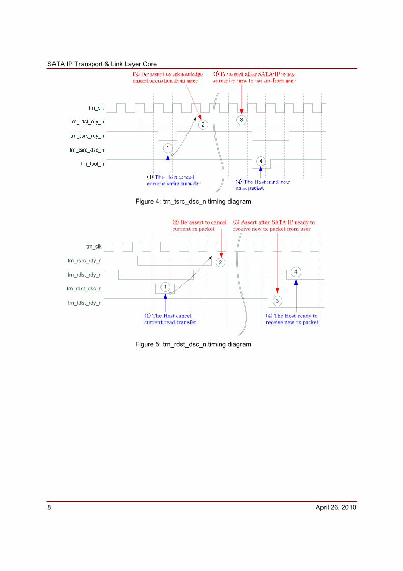
trn_tsrc_dsc_n In Transmit Source Abort: Assert 1 clock period of trn_clk during operation (between tsof and teof)
when the Host requires to cancel current write operation. Active low. After asserted, the Core will
send SYNC primitive to SATA-PHY for abort the current transfer. The Host needs to wait until
trn_tdst_rdy_n ready again before sending next packet. See Figure 4 for more details.
trn_tdst_dsc_n Out Transmit Destination Abort: Assert 1 clock period of trn_clk from the Core to cancel current write
operation when SYNC primitive is received during data write operation. Active low. See Figure 6
for more details.
Design Gateway Co., Ltd.
April 26, 2010 5
Signal Signal
Direction Description
Receive Transaction Interface
trn_rsof_n Out Receive Start-Of-Frame (SOF): Indicate start each SATA FIS packet. Active low.
trn_reof_n Out Receive End-Of-Frame (EOF): Indicate end each SATA FIS packet. Active low.
trn_rd[31:0] Out Receive Data: SATA FIS packet data to be received.
trn_rsrc_rdy_n Out Receive Source Ready: Indicates that trn_rd[31:0] from the core is valid. Active low.
trn_rdst_rdy_n In Receive Destination Ready: Indicate that the Host is ready to accept data on trn_rd[31:0]. Active
low. trn_rsrc_rdy_n will be de-asserted within 4 period of trn_clk after trn_rdst_rdy_n is de-
asserted. So Host should be supported to accept 4 DWORD of trn_rd[31:0] after trn_rdst_rdy_n is
de-asserted.
trn_rsrc_dsc_n Out Receive Source Abort: Assert 1 clock period of trn_clk from the Core to cancel current read
operation when SYNC primitive is received during data read operation. Active low. See Figure 7 for
more details.
trn_rdst_dsc_n In Receive Destination Abort: Assert 1 clock period of trn_clk during read operation (between rsof and
reof) when the Host requires to cancel current read operation. Active low. After asserted, the core
will send SYNC primitive to SATA-PHY for abort the current transfer. The Host needs to wait until
trn_tdst_rdy_n ready again before sending next packet. See Figure 5 for more details.
SATA PHY Interface for Virtex6 GTX
PHYRESET In Not used now.
PHYCLK In Reference Clock for 16-bit SATA PHY (Virtex6 GTX)
- 150MHz for SATA-II
This clock is generated from DCM inside SATA PHY. It’s used for both both TX and RX data by
elastic buffer in GTX of SATA PHY.
TXDATA[15:0] Out 16-bit transmit data from the core to the GTX
TXDATAK[1:0] Out 2-bit Data/Control for the symbols of transmitted data.
(“00”: data byte, “01”: control byte, “1X”: reserved).
RXDATA[15:0] In 16-bit receive data from the GTX to the core.
RXDATAK[1:0] In 2-bit Data/Control for the symbols of received data.
(“00”: data byte, “01”: control byte, “1X”: reserved)
RXDATAVALID In Not used now.
LINKUP In Indicates that SATA link communication is established. Active high.
PLLLOCK In Indicates that DCM of GTX is locked. Active high.
SATA IP Transport & Link Layer Core
6 April 26, 2010
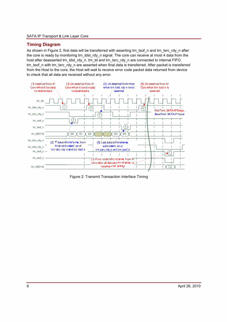
Timing Diagram
As shown in Figure 2, first data will be transferred with asserting trn_tsof_n and trn_tsrc_rdy_n after
the core is ready by monitoring trn_tdst_rdy_n signal. The core can receive at most 4 data from the
host after deasserted trn_tdst_rdy_n. trn_td and trn_tsrc_rdy_n are connected to internal FIFO.
trn_teof_n with trn_tsrc_rdy_n are asserted when final data is transferred. After packet is transferred
from the Host to the core, the Host will wait to receive error code packet data returned from device
to check that all data are received without any error.
Figure 2: Transmit Transaction Interface Timing

Design Gateway Co., Ltd.
April 26, 2010 7
Similar to Figure 2, first data will be transferred from the core after trn_rdst_rdy_n signal is asserted.
trn_rdst_rdy_n signal must be deasserted before data buffer inside the Host is full at least 4 clock
period. After packet is transferred from the core to the Host, the Host will wait to receive error code
packet data returned from device.
Figure 3: Receive Transaction Interface Timing
Error code which is shown in timing diagram is designed for the Host to check that current data packet can be transferred completely or not. So, the Host should be checked error code value after end transfer. The detail of error code is shown in Table3.
Table 3: Error code description.
Bit Signal
Name Description
[31:27] Reserved Always zero
[26] Dir Current transfer direction flag. ‘0’: From the Host to SATA IP, ‘1’: From SATA IP to the Host
[25:24] Error Error code flag.
“00”: No error
“01”: Bad/Unknown SATA FIS packet. WTRM primitive is received during read operation or R_ERR
primitive is received at the end of write operation. Please check data packet is correct format or not
when this error detected.
“10”: CRC error. Please check SATA signal quality when this error detected.
“11”: Reserved
[23:8] Reserved Always zero
[7:0] FIS Type This byte indicates the header of error code packet. “0xEF” is defined to be different from other
SATA FIS.
SATA IP Transport & Link Layer Core
8 April 26, 2010
Figure 4: trn_tsrc_dsc_n timing diagram
trn_clk
trn_rsrc_rdy_n
trn_rdst_dsc_n
trn_tdst_rdy_n
trn_rdst_rdy_n
1
2
3
(1) The Host cancel current read transfer
(2) De-assert to cancel current rx packet
(3) Assert after SATA-IP ready to receive new tx packet from user
4
(4) The Host ready to receive new rx packet
Figure 5: trn_rdst_dsc_n timing diagram

Design Gateway Co., Ltd.
April 26, 2010 9
Figure 6: trn_tdst_dsc_n timing diagram
Figure 7: trn_rsrc_dsc_n timing diagram

SATA IP Transport & Link Layer Core
10 April 26, 2010
Verification Methods
The SATA IP Core functionality was verified by simulation and also proved on real board design by
using ML605 evaluation board.
Recommended Design Experience
Experience design engineers with a knowledge of RocketIO and Xilinx’s EDK should easily integrate
this IP into their design. For user board development, compliance with design guideline described in
UG366 (Virtex-6 FPGA GTX Transceivers User Guide) is strongly recommended.
Ordering Information
This product is available directly from Design Gateway Co., Ltd. Please contact Design Gatway Co.,
Ltd. for pricing and additional information about this product using the contact information on the
front page of this datasheet.
Revision History
Revision Date Description
1.0 Apr-26-2010 New release


