SAMPLE CHAPTER 1 - Wiley India - Books & eSolutions …ŸBus slots NßPCI NßAGP NßPCIe NßAMR...
86
SAMPLE CHAPTER 1
Transcript of SAMPLE CHAPTER 1 - Wiley India - Books & eSolutions …ŸBus slots NßPCI NßAGP NßPCIe NßAMR...

SAMPLE CHAPTER 1

Chapter
1Personal Computer System Components
THE FOLLOWING COMPTIA A+ ESSENTIALS EXAM OBJECTIVES ARE COVERED IN THIS CHAPTER:
1.2 Explain motherboard components, types and features
Form Factor
ATX / BTX,
micro ATX
NLX
I/O interfaces
Sound
Video
USB 1.1 and 2.0
Serial
IEEE 1394 / FireWire
Parallel
NIC
Modem
PS/2
Memory slots
RIMM
DIMM
SODIMM
SIMM
Processor sockets
Bus architecture
86498book.indb 1 7/22/09 5:37:17 AM
Copyrighted
Mate
rial

Bus slots
PCI
AGP
PCIe
AMR
CNR
PCMCIA Chipsets
BIOS / CMOS / Firmware
POST
CMOS battery
Riser card / daughterboard
[Additional subobjectives covered in chapter 2]
1.4 Explain the purpose and characteristics of CPUs and
their features
Identify CPU types
AMD
Intel
Hyper threading
Multi core
Dual core
Triple core
Quad core
Onchip cache
L1
L2
Speed (real vs. actual)
32 bit vs. 64 bit
1.5 Explain cooling methods and devices
Heat sinks
CPU and case fans
86498book.indb 2 7/22/09 5:37:18 AM
Liquid cooling systems
Thermal compound
1.6 Compare and contrast memory types, characteristics
and their purpose
Types
DRAM
SRAM
SDRAM
DDR / DDR2 / DDR3
RAMBUS
Parity vs. Non-parity
ECC vs. non-ECC
Single sided vs. double sided
Single channel vs. dual channel
Speed
PC100
PC133
PC2700
PC3200
DDR3-1600
DDR2-667
86498book.indb 3 7/22/09 5:37:19 AM
A personal computer (PC) is a computing device made up of many distinct electronic components that all function together in order to accomplish some useful task (such as adding up the
numbers in a spreadsheet or helping you write a letter). Note that this definition describes a computer as having many distinct parts that work together. Most computers today are modular. That is, they have components that can be removed and replaced with a compo-nent of similar function in order to improve performance. Each component has a specific function. In this chapter, you will learn about the components that make up a typical PC, what their functions are, and how they work together inside the PC.
Unless specifically mentioned otherwise, throughout this book the terms PC and computer can be used interchangeably.
In this chapter, you will learn how to identify system components common to most personal computers, including the following:
Motherboards
Processors
Memory
Cooling systems
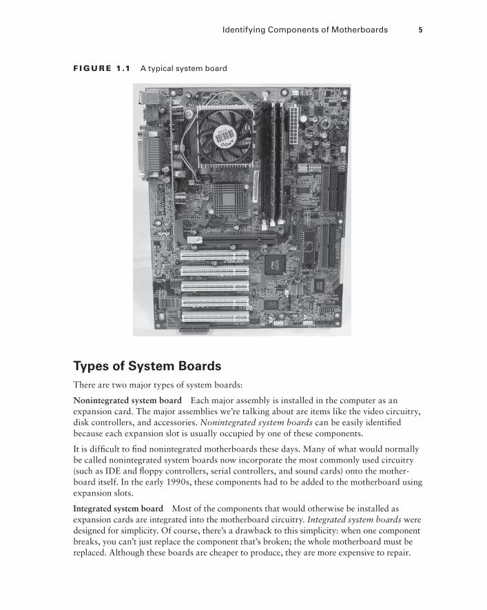
Identifying Components of MotherboardsThe spine of the computer is the motherboard, otherwise known as the system board (and less commonly referred to as the planar board). This is the olive green or brown circuit board that lines the bottom of the computer. It is the most important component in the computer because it connects all the other components of a PC together. Figure 1.1 shows a typical PC system board, as seen from above. All other components are attached to this circuit board. On the system board, you will find the central processing unit (CPU), underlying circuitry, expansion slots, video components, random access memory (RAM) slots, and a variety of other chips.
86498book.indb 4 7/22/09 5:37:19 AM
Identifying Components of Motherboards 5
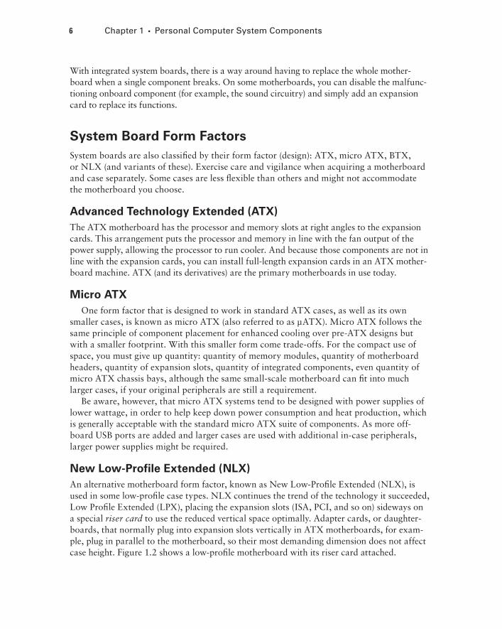
F I GU R E 1.1 A typical system board
Types of System Boards
There are two major types of system boards:
Nonintegrated system board Each major assembly is installed in the computer as an expansion card. The major assemblies we’re talking about are items like the video circuitry, disk controllers, and accessories. Nonintegrated system boards can be easily identified because each expansion slot is usually occupied by one of these components.
It is difficult to find nonintegrated motherboards these days. Many of what would normally be called nonintegrated system boards now incorporate the most commonly used circuitry (such as IDE and floppy controllers, serial controllers, and sound cards) onto the mother-board itself. In the early 1990s, these components had to be added to the motherboard using expansion slots.
Integrated system board Most of the components that would otherwise be installed as expansion cards are integrated into the motherboard circuitry. Integrated system boards were designed for simplicity. Of course, there’s a drawback to this simplicity: when one component breaks, you can’t just replace the component that’s broken; the whole motherboard must be replaced. Although these boards are cheaper to produce, they are more expensive to repair.
86498book.indb 5 7/22/09 5:37:20 AM
6 Chapter 1 Personal Computer System Components
With integrated system boards, there is a way around having to replace the whole mother-board when a single component breaks. On some motherboards, you can disable the malfunc-tioning onboard component (for example, the sound circuitry) and simply add an expansion card to replace its functions.
System Board Form Factors
System boards are also classified by their form factor (design): ATX, micro ATX, BTX, or NLX (and variants of these). Exercise care and vigilance when acquiring a motherboard and case separately. Some cases are less flexible than others and might not accommodate the motherboard you choose.
Advanced Technology Extended (ATX)
The ATX motherboard has the processor and memory slots at right angles to the expansion cards. This arrangement puts the processor and memory in line with the fan output of the power supply, allowing the processor to run cooler. And because those components are not in line with the expansion cards, you can install full-length expansion cards in an ATX mother-board machine. ATX (and its derivatives) are the primary motherboards in use today.
Micro ATX
One form factor that is designed to work in standard ATX cases, as well as its own smaller cases, is known as micro ATX (also referred to as μATX). Micro ATX follows the same principle of component placement for enhanced cooling over pre-ATX designs but with a smaller footprint. With this smaller form come trade-offs. For the compact use of space, you must give up quantity: quantity of memory modules, quantity of motherboard headers, quantity of expansion slots, quantity of integrated components, even quantity of micro ATX chassis bays, although the same small-scale motherboard can fit into much larger cases, if your original peripherals are still a requirement.
Be aware, however, that micro ATX systems tend to be designed with power supplies of lower wattage, in order to help keep down power consumption and heat production, which is generally acceptable with the standard micro ATX suite of components. As more off-board USB ports are added and larger cases are used with additional in-case peripherals, larger power supplies might be required.
New Low-Profile Extended (NLX)
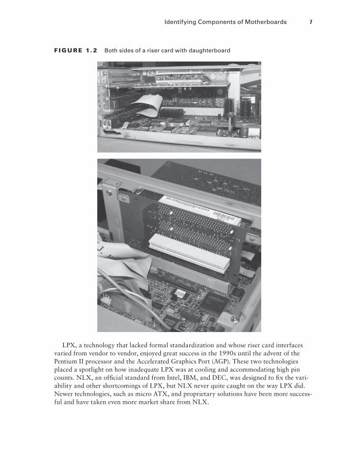
An alternative motherboard form factor, known as New Low-Profile Extended (NLX), is used in some low-profile case types. NLX continues the trend of the technology it succeeded, Low Profile Extended (LPX), placing the expansion slots (ISA, PCI, and so on) sideways on a special riser card to use the reduced vertical space optimally. Adapter cards, or daughter-boards, that normally plug into expansion slots vertically in ATX motherboards, for exam-ple, plug in parallel to the motherboard, so their most demanding dimension does not affect case height. Figure 1.2 shows a low-profile motherboard with its riser card attached.
86498book.indb 6 7/22/09 5:37:20 AM
Identifying Components of Motherboards 7
F I GU R E 1. 2 Both sides of a riser card with daughterboard
LPX, a technology that lacked formal standardization and whose riser card interfaces varied from vendor to vendor, enjoyed great success in the 1990s until the advent of the Pentium II processor and the Accelerated Graphics Port (AGP). These two technologies placed a spotlight on how inadequate LPX was at cooling and accommodating high pin counts. NLX, an official standard from Intel, IBM, and DEC, was designed to fix the vari-ability and other shortcomings of LPX, but NLX never quite caught on the way LPX did. Newer technologies, such as micro ATX, and proprietary solutions have been more success-ful and have taken even more market share from NLX.
86498book.indb 7 7/22/09 5:37:21 AM
8 Chapter 1 Personal Computer System Components
Balanced Technology Extended (BTX)
In 2003, Intel announced its design for a new motherboard, slated to hit the market mid- to late-2004. When that time came, the new BTX motherboard was met with mixed reactions. (Let’s postpone accusations of acronym reverse-engineering until “CTX” is announced as the name of the next generation.) Intel and its consumers realized that the price for faster components that produced more heat would be a retooling of the now-classic (since mid-1990s) ATX design. The motherboard manufacturers saw research and development expense and potential profit loss simply to accommodate the next generation of hotter-running processors, processors manufactured by the same designers of the BTX technology. It was this resistance that caused the BTX form factor to gain very little ground over the next couple of years. Nevertheless, with the early support of Gateway, and later buy-in of Dell, the BTX design dug in and charted a path for future success.
Marketing aside, the BTX technology is well thought out and serves the purpose for which it was intended. By lining up all heat-producing components between air intake vents and the power supply’s exhaust fan, Intel found that the CPU and other components could be cooled properly by passive heat sinks. A heat sink is a block of aluminum or other metal, with veins throughout, that sits on top of the CPU, drawing its heat away. Fewer fans and a more efficient airflow path create a quieter configuration overall. While the BTX design benefits any modern onboard implementation, Intel’s recommitment to lower-power CPUs has at once lessened the need to rush to more expensive BTX systems and given the market a bit more time to assimilate this newer technology.
There are other motherboard designs, but these are the most popular and also the ones that are covered on the exam. Some manufacturers (such as Compaq and IBM) design and manufacture their own motherboards, which don’t conform to the standards. This style of motherboard is known as a motherboard of proprietary design.
System Board Components
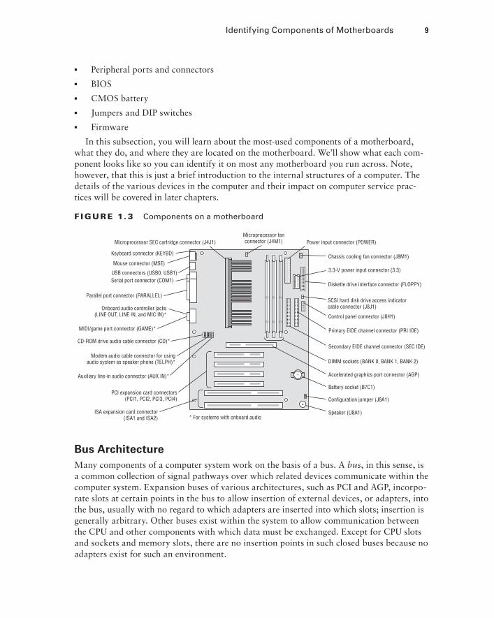
Now that you understand the basic types of motherboards and their form factors, it’s time to look at the components found on the motherboard and their locations relative to each other. Figure 1.3 illustrates many of the following components found on a typical motherboard:
Chipsets
Expansion slots and buses
Memory slots and external cache
CPU and processor slots or sockets
Power connectors
Onboard disk drive connectors
Keyboard connectors
86498book.indb 8 7/22/09 5:37:21 AM
Identifying Components of Motherboards 9
Peripheral ports and connectors
BIOS
CMOS battery
Jumpers and DIP switches
Firmware
In this subsection, you will learn about the most-used components of a motherboard, what they do, and where they are located on the motherboard. We’ll show what each com-ponent looks like so you can identify it on most any motherboard you run across. Note, however, that this is just a brief introduction to the internal structures of a computer. The details of the various devices in the computer and their impact on computer service prac-tices will be covered in later chapters.
F I GU R E 1. 3 Components on a motherboard
Keyboard connector (KEYBD)
USB connectors (USB0, USB1)Serial port connector (COM1)
Parallel port connector (PARALLEL)
MIDI/game port connector (GAME)*
Auxiliary line-in audio connector (AUX IN)*
* For systems with onboard audioISA expansion card connector
(ISA1 and ISA2)
PCI expansion card connectors(PCI1, PCI2, PCI3, PCI4)
Modem audio cable connector for usingaudio system as speaker phone (TELPH)*
CD-ROM drive audio cable connector (CD)*
Onboard audio controller jacks(LINE OUT, LINE IN, and MIC IN)*
Mouse connector (MSE)
Power input connector (POWER)Microprocessor fanconnector (J4M1)
Chassis cooling fan connector (J8M1)
3.3-V power input connector (3.3)
Diskette drive interface connector (FLOPPY)
Control panel connector (J8H1)
Secondary EIDE channel connector (SEC IDE)
Accelerated graphics port connector (AGP)
Battery socket (B7C1)
Configuration jumper (J8A1)
Speaker (U8A1)
DIMM sockets (BANK 0, BANK 1, BANK 2)
Primary EIDE channel connector (PRI IDE)
SCSI hard disk drive access indicatorcable connector (J8J1)
Microprocessor SEC cartridge connector (J4J1)
Bus Architecture
Many components of a computer system work on the basis of a bus. A bus, in this sense, is a common collection of signal pathways over which related devices communicate within the computer system. Expansion buses of various architectures, such as PCI and AGP, incorpo-rate slots at certain points in the bus to allow insertion of external devices, or adapters, into the bus, usually with no regard to which adapters are inserted into which slots; insertion is generally arbitrary. Other buses exist within the system to allow communication between the CPU and other components with which data must be exchanged. Except for CPU slots and sockets and memory slots, there are no insertion points in such closed buses because no adapters exist for such an environment.
86498book.indb 9 7/22/09 5:37:22 AM
10 Chapter 1 Personal Computer System Components
The term bus is also used in any parallel or bit-serial wiring implementation where multi-ple devices can be attached at the same time in parallel or in series (daisy-chained). Examples include Universal Serial Bus (USB), Small Computer System Interface (SCSI), and Ethernet.
Chipsets
A chipset is a collection of chips or circuits that perform interface and peripheral functions for the processor. This collection of chips is usually the circuitry that provides interfaces for memory, expansion cards, and onboard peripherals and generally dictates how a mother-board will communicate with the installed peripherals.
Chipsets are usually given a name and model number by the original manufacturer. For example, if you see that a motherboard has a VIA KT7 chipset, you would know that the circuitry for controlling peripherals was designed by VIA and was given the designation KT7. Typically, the manufacturer and model also tell you that your particular chipset has a certain set of features (for example, onboard video of a certain type/brand, onboard audio of a particular type, and so on).
Chipsets can be made up of one or several integrated circuit chips. Intel-based moth-erboards typically use two chips, whereas the SiS chipsets typically use one. To know for sure, you must check the manufacturer’s documentation.
The functions of chipsets can be divided into two major functional groups, called Northbridge and Southbridge. Let’s take a brief look at these groups and the functions they perform.
Northbridge
The Northbridge subset of a motherboard’s chipset is the set of circuitry or chips that per-forms one very important function: management of high-speed peripheral communications. The Northbridge subset is responsible primarily for communications with integrated video using AGP and PCI Express, for instance, and processor-to-memory communications. There-fore, it can be said that much of the true performance of a PC relies on the specifications of the Northbridge component and its communications capability with the peripherals it controls.
When we use the term Northbridge, we are referring to the set of chips and circuits that make up a particular subset of a motherboard’s chipset. There isn’t actually a Northbridge brand of chipset.
The communications between the CPU and memory occur over what is known as the frontside bus (FSB), which is just a set of signal pathways between the CPU and main memory. The clock signal that drives the FSB is used to drive communications by certain other devices, such as AGP and PCI Express slots, making them local-bus technologies. The backside bus (BSB), if present, is a set of signal pathways between the CPU and Level 2 or 3 cache memory. The BSB uses the same clock signal that drives the FSB. If no backside bus exists, cache is placed on the frontside bus with the CPU and main memory.
The Northbridge is directly connected to the Southbridge (discussed next) and helps to manage the communications between the Southbridge and the rest of the computer.
86498book.indb 10 7/22/09 5:37:22 AM
Identifying Components of Motherboards 11
Southbridge
The Southbridge subset of the chipset, as mentioned earlier, is responsible for providing support to the myriad onboard slower peripherals (PS/2, Parallel, IDE, and so on), manag-ing their communications with the rest of the computer and the resources given to them. These components do not need to keep up with the external clock of the CPU and do not represent a bottleneck in the overall performance of the system. Any component that would impose such a restriction on the system should eventually be developed for FSB attachment.
Most motherboards today have integrated PS/2, USB, Parallel, and Serial. Some of the optional features handled by the Southbridge include LAN, audio, infrared, and FireWire (IEEE 1394). When first integrated, the quality of onboard audio was marginal at best, but the latest offerings rival external sound adapters in sound quality and number of features (including Dolby Digital Theater Surround technology, among others).
The Southbridge is also responsible for managing communications with the other expan-sion buses, such as PCI, USB, and legacy buses.
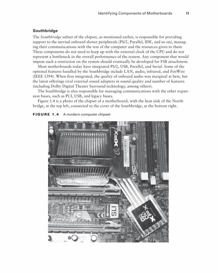
Figure 1.4 is a photo of the chipset of a motherboard, with the heat sink of the North-bridge, at the top left, connected to the cover of the Southbridge, at the bottom right.
F I GU R E 1. 4 A modern computer chipset
86498book.indb 11 7/22/09 5:37:22 AM
12 Chapter 1 Personal Computer System Components
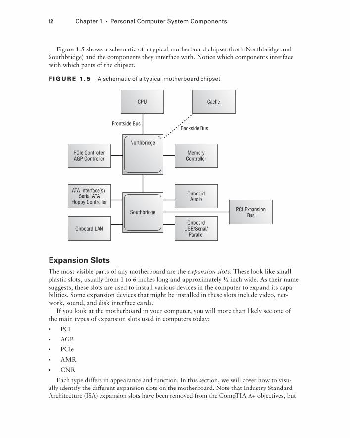
Figure 1.5 shows a schematic of a typical motherboard chipset (both Northbridge and Southbridge) and the components they interface with. Notice which components interface with which parts of the chipset.
F I GU R E 1.5 A schematic of a typical motherboard chipset
Southbridge
ATA Interface(s) Serial ATA
Floppy Controller
PCIe ControllerAGP Controller
Onboard LAN
OnboardAudio
MemoryController
OnboardUSB/Serial/
Parallel
PCI ExpansionBus
CPU Cache
Northbridge
Backside BusFrontside Bus
Expansion Slots
The most visible parts of any motherboard are the expansion slots. These look like small plastic slots, usually from 1 to 6 inches long and approximately ½ inch wide. As their name suggests, these slots are used to install various devices in the computer to expand its capa-bilities. Some expansion devices that might be installed in these slots include video, net-work, sound, and disk interface cards.
If you look at the motherboard in your computer, you will more than likely see one of the main types of expansion slots used in computers today:
PCI
AGP
PCIe
AMR
CNR
Each type differs in appearance and function. In this section, we will cover how to visu-ally identify the different expansion slots on the motherboard. Note that Industry Standard Architecture (ISA) expansion slots have been removed from the CompTIA A+ objectives, but
86498book.indb 12 7/22/09 5:37:23 AM
Identifying Components of Motherboards 13
you might wish to research these slots for your own edification and to be prepared, should you find yourself face to face with such a beast in the field. PC Card buses, such as PCMCIA, are related more to laptops than to desktop computers and are covered in Chapter 4.
PCI Expansion Slots
Many computers in force today contain 32-bit Peripheral Component Interconnect (PCI) slots. They are easily recognizable because they are short (around 3 inches long), compared to the classic ISA slot, and usually white. PCI slots can usually be found in any computer that has a Pentium-class processor or higher. PCI expansion buses operate at 33 or 66MHz over a 32-bit (4-byte) channel, resulting in data rates of 133 and 266MBps, respectively, with 133MBps the most common, server architectures excluded. Servers often feature 64-bit slots as well, which double the 32-bit data rates.
PCI slots and adapters are manufactured in 3.3 and 5V versions. Universal adapters are keyed to fit in slots based on either of the two voltages. The notch in the card edge of the com-mon 5V slots and adapters is oriented toward the front of the motherboard, and the notch in the 3.3V adapters toward the rear. Figure 1.6 shows several PCI expansion slots. Note the 5V 32-bit slot in the foreground and the 3.3V 64-bit slots. Also notice that a universal 32-bit card fits fine in the 64-bit 3.3V slot.
F I GU R E 1.6 PCI expansion slots
AGP Expansion Slots
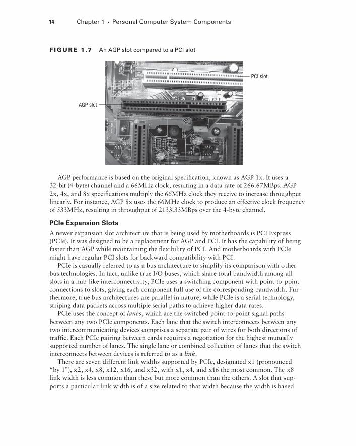
Accelerated Graphics Port (AGP) slots are known mostly for video card use and are steadily being supplanted by PCI Express adapters. In the past, if you wanted to use a high-speed, accelerated 3D graphics video card, you had to install the card into an exist-ing PCI or ISA slot. AGP slots were designed to be a direct connection between the video circuitry and the PC’s memory. They are also easily recognizable because they are usually brown, are located right next to the PCI slots on the motherboard, and are slightly shorter than the PCI slots.
Another landmark to look for when identifying later AGP slots is the often alternate-colored shell surrounding the slot with an extension toward the front of the system that snaps into place at the “rear” of the adapter. It is necessary to pull the extension away from the adapter before removing it from the slot. Figure 1.7 shows an example of an AGP slot, along with a PCI slot for comparison. Notice the difference in length between the two.
86498book.indb 13 7/22/09 5:37:24 AM
14 Chapter 1 Personal Computer System Components
F I GU R E 1.7 An AGP slot compared to a PCI slot
PCI slot
AGP slot
AGP performance is based on the original specification, known as AGP 1x. It uses a 32-bit (4-byte) channel and a 66MHz clock, resulting in a data rate of 266.67MBps. AGP 2x, 4x, and 8x specifications multiply the 66MHz clock they receive to increase throughput linearly. For instance, AGP 8x uses the 66MHz clock to produce an effective clock frequency of 533MHz, resulting in throughput of 2133.33MBps over the 4-byte channel.
PCIe Expansion Slots
A newer expansion slot architecture that is being used by motherboards is PCI Express (PCIe). It was designed to be a replacement for AGP and PCI. It has the capability of being faster than AGP while maintaining the flexibility of PCI. And motherboards with PCIe might have regular PCI slots for backward compatibility with PCI.
PCIe is casually referred to as a bus architecture to simplify its comparison with other bus technologies. In fact, unlike true I/O buses, which share total bandwidth among all slots in a hub-like interconnectivity, PCIe uses a switching component with point-to-point connections to slots, giving each component full use of the corresponding bandwidth. Fur-thermore, true bus architectures are parallel in nature, while PCIe is a serial technology, striping data packets across multiple serial paths to achieve higher data rates.
PCIe uses the concept of lanes, which are the switched point-to-point signal paths between any two PCIe components. Each lane that the switch interconnects between any two intercommunicating devices comprises a separate pair of wires for both directions of traffic. Each PCIe pairing between cards requires a negotiation for the highest mutually supported number of lanes. The single lane or combined collection of lanes that the switch interconnects between devices is referred to as a link.
There are seven different link widths supported by PCIe, designated x1 (pronounced “by 1”), x2, x4, x8, x12, x16, and x32, with x1, x4, and x16 the most common. The x8 link width is less common than these but more common than the others. A slot that sup-ports a particular link width is of a size related to that width because the width is based
86498book.indb 14 7/22/09 5:37:25 AM
Identifying Components of Motherboards 15
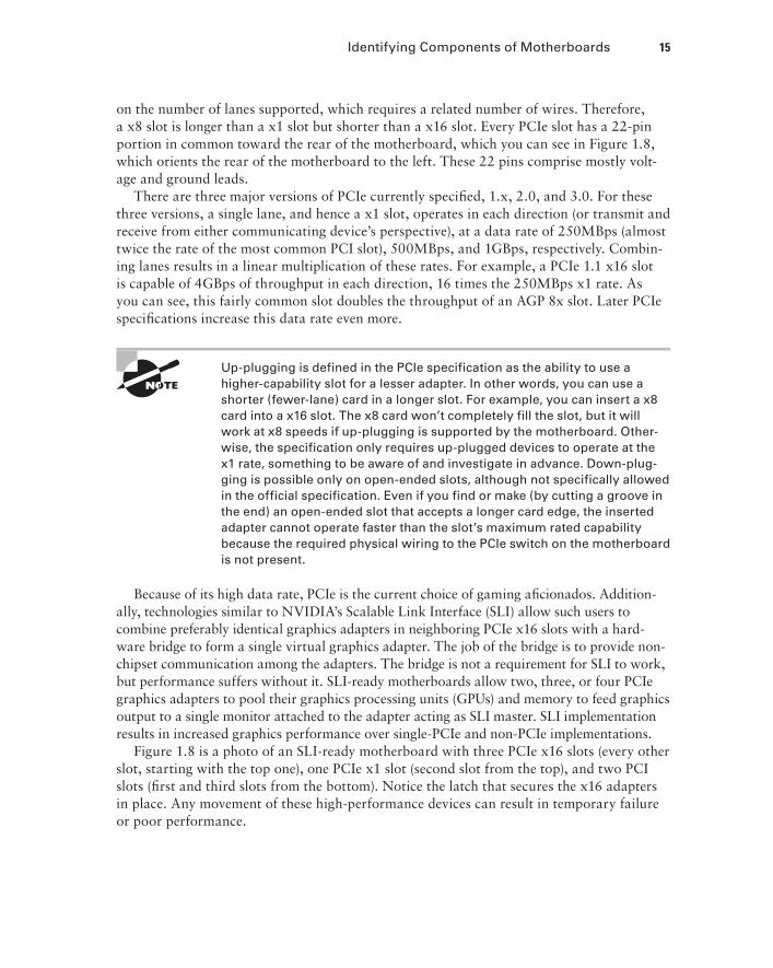
on the number of lanes supported, which requires a related number of wires. Therefore, a x8 slot is longer than a x1 slot but shorter than a x16 slot. Every PCIe slot has a 22-pin portion in common toward the rear of the motherboard, which you can see in Figure 1.8, which orients the rear of the motherboard to the left. These 22 pins comprise mostly volt-age and ground leads.
There are three major versions of PCIe currently specified, 1.x, 2.0, and 3.0. For these three versions, a single lane, and hence a x1 slot, operates in each direction (or transmit and receive from either communicating device’s perspective), at a data rate of 250MBps (almost twice the rate of the most common PCI slot), 500MBps, and 1GBps, respectively. Combin-ing lanes results in a linear multiplication of these rates. For example, a PCIe 1.1 x16 slot is capable of 4GBps of throughput in each direction, 16 times the 250MBps x1 rate. As you can see, this fairly common slot doubles the throughput of an AGP 8x slot. Later PCIe specifications increase this data rate even more.
Up-plugging is defined in the PCIe specification as the ability to use a higher-capability slot for a lesser adapter. In other words, you can use a shorter (fewer-lane) card in a longer slot. For example, you can insert a x8 card into a x16 slot. The x8 card won’t completely fill the slot, but it will work at x8 speeds if up-plugging is supported by the motherboard. Other-wise, the specification only requires up-plugged devices to operate at the x1 rate, something to be aware of and investigate in advance. Down-plug-ging is possible only on open-ended slots, although not specifically allowed in the official specification. Even if you find or make (by cutting a groove in the end) an open-ended slot that accepts a longer card edge, the inserted adapter cannot operate faster than the slot’s maximum rated capability because the required physical wiring to the PCIe switch on the motherboard is not present.
Because of its high data rate, PCIe is the current choice of gaming aficionados. Addition-ally, technologies similar to NVIDIA’s Scalable Link Interface (SLI) allow such users to combine preferably identical graphics adapters in neighboring PCIe x16 slots with a hard-ware bridge to form a single virtual graphics adapter. The job of the bridge is to provide non-chipset communication among the adapters. The bridge is not a requirement for SLI to work, but performance suffers without it. SLI-ready motherboards allow two, three, or four PCIe graphics adapters to pool their graphics processing units (GPUs) and memory to feed graphics output to a single monitor attached to the adapter acting as SLI master. SLI implementation results in increased graphics performance over single-PCIe and non-PCIe implementations.
Figure 1.8 is a photo of an SLI-ready motherboard with three PCIe x16 slots (every other slot, starting with the top one), one PCIe x1 slot (second slot from the top), and two PCI slots (first and third slots from the bottom). Notice the latch that secures the x16 adapters in place. Any movement of these high-performance devices can result in temporary failure or poor performance.
86498book.indb 15 7/22/09 5:37:25 AM
16 Chapter 1 Personal Computer System Components
F I GU R E 1. 8 PCIe expansion slots
AMR Expansion Slots
As is always the case, Intel and other manufacturers are constantly looking for ways to improve the production process. One lengthy process that would often slow down the pro-duction of motherboards with integrated analog I/O functions was FCC certification. The manufacturers developed a way of separating the analog circuitry, for example, modem and analog audio, onto its own card. This allowed the analog circuitry to be separately certified (it was its own expansion card), thus reducing time for FCC certification.
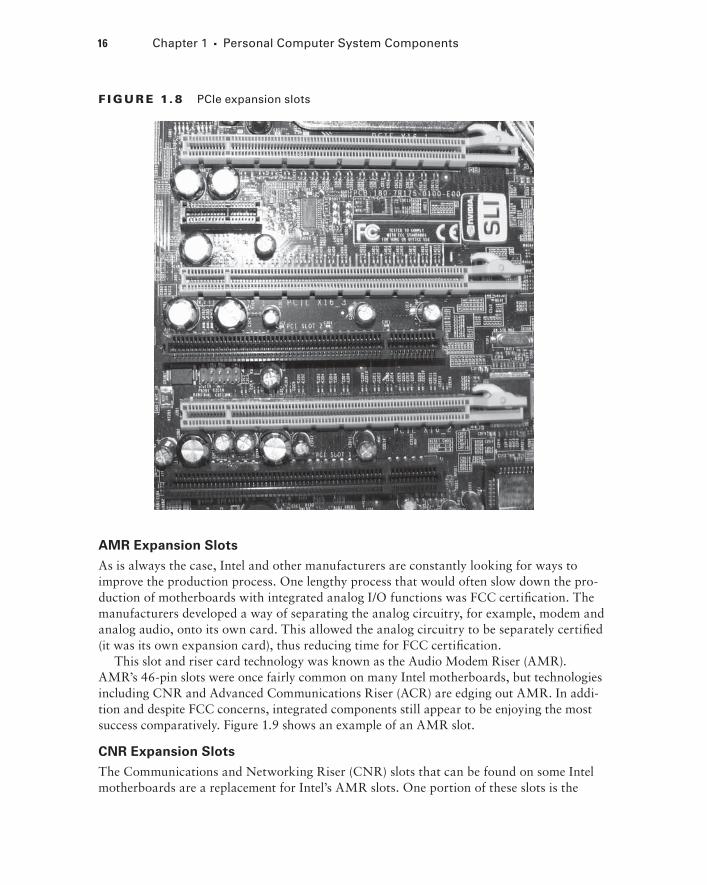
This slot and riser card technology was known as the Audio Modem Riser (AMR). AMR’s 46-pin slots were once fairly common on many Intel motherboards, but technologies including CNR and Advanced Communications Riser (ACR) are edging out AMR. In addi-tion and despite FCC concerns, integrated components still appear to be enjoying the most success comparatively. Figure 1.9 shows an example of an AMR slot.
CNR Expansion Slots
The Communications and Networking Riser (CNR) slots that can be found on some Intel motherboards are a replacement for Intel’s AMR slots. One portion of these slots is the
86498book.indb 16 7/22/09 5:37:25 AM
Identifying Components of Motherboards 17
same length as one of the portions of the AMR slot, but the other portion of the CNR slot is longer than that of the AMR slot. Essentially, these 60-pin slots allow a motherboard manufacturer to implement a motherboard chipset with certain integrated features. Then, if the built-in features of that chipset need to be enhanced (by adding Dolby Digital Surround to a standard sound chipset, for example), a CNR riser card could be added to enhance the onboard capabilities. Additional advantages of CNR over AMR include networking sup-port, Plug and Play compatibility, support for hardware acceleration (as opposed to CPU control only), and the fact that there’s no need to lose a competing PCI slot unless the CNR slot is in use. Figure 1.10 shows an example of a CNR slot (arrow).
F I GU R E 1. 9 An AMR slot
Memory Slots and Cache
Memory, or random access memory (RAM), slots are the next most prolific slots on a motherboard, and they contain the modules that hold memory chips that make up primary memory, the memory used to store currently used data and instructions for the CPU. Many and varied types of memory are available for PCs today. In this chapter, you will become familiar with the appearance and specifications of the slots on the motherboard, so you can identify them.
For the most part, PCs today use memory chips arranged on a small circuit board. Certain of these circuit boards are called dual inline memory modules (DIMMs). Today’s DIMMs differ in the number of conductors, or pins, that the particular physical specifi-cation uses. Some common examples include 168-, 184-, and 240-pin configurations. In addition, laptop memory comes in smaller form factors known as small outline DIMMs (SODIMMs) and MicroDIMMs. The single inline memory module (SIMM) is an older memory form factor that we’ll discuss shortly. More detail on memory packaging and the technologies that use them can be found later in this chapter in the section “Identifying Purposes and Characteristics of Memory.” Figure 1.11 shows the form factors for some popular memory modules. Notice how they basically look the same but the module sizes and keying notches are different.
86498book.indb 17 7/22/09 5:37:26 AM

18 Chapter 1 Personal Computer System Components
F I GU R E 1.10 A CNR slot
F I GU R E 1.11 Different memory module form factors
30-pin SIMM (3.5 .75˝ )
144-pin SODIMM (2.625 1˝ ) 72-pin SODIMM (2.375 1˝ )
72-pin SIMM (4.25 1˝ )
168-pin DIMM (5.375 1˝ )
Memory slots are easy to identify on a motherboard. DIMM slots are usually black and placed very close together. DIMM slots with pair-by-pair color coding can be observed these days, however. Generally, the pairs of slots must be filled together for best performance or to work at all, in some cases. Consult the motherboard’s documentation to determine the specific modules allowed as well as their required orientation. The number of memory slots varies from motherboard to motherboard, but the structure of the different slots is similar. Metal pins in the bottom make contact with the metallic pins on each memory module. Small metal or plastic tabs on each side of the slot keep the memory module securely in its slot.
86498book.indb 18 7/22/09 5:37:27 AM
Identifying Components of Motherboards 19
Sometimes the amount of primary memory installed is inadequate to service additional requests for memory resources from newly launched applications. When this condition occurs, the user receives an “out of memory” error, and the application fails to launch. One solution for this is to use the hard drive as additional RAM. This space on the hard drive is known as a swap file or a paging file. The technology in general is known as virtual memory. The swap file, in modern Microsoft operating systems, is a contigu-ous, optimized space that can deliver information to RAM at the request of the memory controller faster than if it came from the general storage pool of the drive. Note that virtual memory cannot be used directly from the hard drive; it must be paged into RAM as the oldest contents of RAM are paged out to the hard drive to make room. The memory con-troller, by the way, is the chip that manages access to RAM, as well as adapters that have had a few hardware addresses reserved for their communication with the processor.
Nevertheless, relying too much on virtual memory (check your page fault statistics in the Reliability and Performance Monitor) results in the entire system slowing down noticeably. An inexpensive and highly effective solution is to add physical memory to the system, thus reducing its reliance on virtual memory. More information on virtual memory and its con-figuration can be found in Chapter 7, “Installing and Configuring Operating Systems.”
When it’s not the size of RAM that you need to enhance but its speed, you can add cache memory on the CPU side of RAM to take care of this. Cache is a very fast form of memory forged from static RAM, which is discussed in detail in the “Identifying Purposes and Characteristics of Memory” section later in this chapter. Cache improves system per-formance by predicting what the CPU will ask for next and prefetching this information before being asked. This paradigm allows the cache to be smaller in size than the RAM itself. Only the most recently used data and code or that which is expected to be used next is stored in cache. Cache on the motherboard is known as external cache because it is exter-nal to the processor, also referred to as Level 2 (L2) cache. Level 1 (L1) cache, by compari-son, is internal cache because it is built into the processor’s silicon wafer.
It is now common for chip makers to use extra space in the processor’s packaging to bring the L2 cache from the motherboard closer to the CPU. When L2 cache is present in the processor’s packaging, the cache on the motherboard is referred to as Level 3 (L3) cache. Unfortunately, due to the de facto naming of cache levels, the term L2 cache alone is not a definitive description of where the cache is located. The terms L1 cache and L3 cache do not vary in their meaning, however. The typical increasing order of capacity and dis-tance from the processor die is L1 cache, L2 cache, L3 cache, RAM. This is also the typical decreasing order of speed.
Central Processing Unit (CPU) and Processor Socket or Slot
The “brain” of any computer is the central processing unit (CPU). There’s no computer without the CPU. There are many different types of processors for computers—so many, in fact, that you will learn about them later in this chapter in the section “Identifying Pur-poses and Characteristics of Processors.”
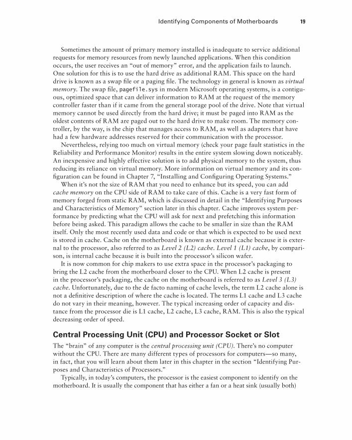
Typically, in today’s computers, the processor is the easiest component to identify on the motherboard. It is usually the component that has either a fan or a heat sink (usually both)
86498book.indb 19 7/22/09 5:37:27 AM
20 Chapter 1 Personal Computer System Components
attached to it (as shown in Figure 1.12). These devices are used to draw away and disperse the heat a processor generates. This is done because heat is the enemy of microelectronics. Theo-retically, a Pentium (or higher) processor generates enough heat that without the heat sink it would permanently damage itself and the motherboard in a matter of hours or even minutes.
F I GU R E 1.12 Two heat sinks, one with a fan
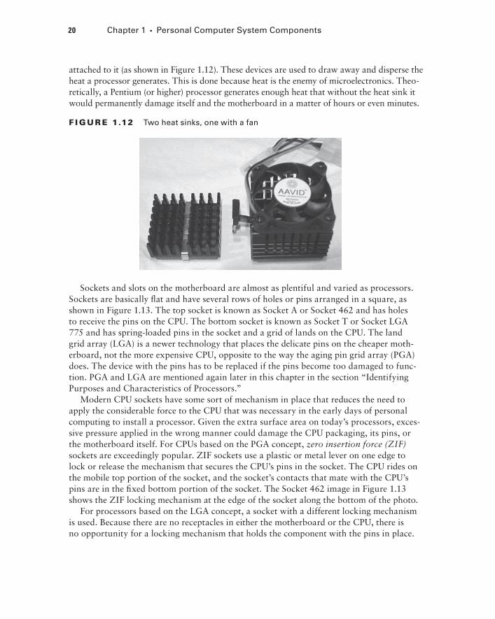
Sockets and slots on the motherboard are almost as plentiful and varied as processors. Sockets are basically flat and have several rows of holes or pins arranged in a square, as shown in Figure 1.13. The top socket is known as Socket A or Socket 462 and has holes to receive the pins on the CPU. The bottom socket is known as Socket T or Socket LGA 775 and has spring-loaded pins in the socket and a grid of lands on the CPU. The land grid array (LGA) is a newer technology that places the delicate pins on the cheaper moth-erboard, not the more expensive CPU, opposite to the way the aging pin grid array (PGA) does. The device with the pins has to be replaced if the pins become too damaged to func-tion. PGA and LGA are mentioned again later in this chapter in the section “Identifying Purposes and Characteristics of Processors.”
Modern CPU sockets have some sort of mechanism in place that reduces the need to apply the considerable force to the CPU that was necessary in the early days of personal computing to install a processor. Given the extra surface area on today’s processors, exces-sive pressure applied in the wrong manner could damage the CPU packaging, its pins, or the motherboard itself. For CPUs based on the PGA concept, zero insertion force (ZIF) sockets are exceedingly popular. ZIF sockets use a plastic or metal lever on one edge to lock or release the mechanism that secures the CPU’s pins in the socket. The CPU rides on the mobile top portion of the socket, and the socket’s contacts that mate with the CPU’s pins are in the fixed bottom portion of the socket. The Socket 462 image in Figure 1.13 shows the ZIF locking mechanism at the edge of the socket along the bottom of the photo.
For processors based on the LGA concept, a socket with a different locking mechanism is used. Because there are no receptacles in either the motherboard or the CPU, there is no opportunity for a locking mechanism that holds the component with the pins in place.
86498book.indb 20 7/22/09 5:37:27 AM
Identifying Components of Motherboards 21
LGA-compatible sockets, as they’re called despite the misnomer, have a lid of sorts that closes over the CPU and is locked in place by an L-shaped arm that borders two of the socket’s edges. The nonlocking leg of the arm has a bend in the middle that latches the lid closed when the other leg of the arm is secured. The bottom image in Figure 1.13 shows an LGA socket with no CPU installed and the locking arm secured over the lid’s tab (right-hand edge in the photo).
F I GU R E 1.13 CPU socket examples
86498book.indb 21 7/22/09 5:37:28 AM
22 Chapter 1 Personal Computer System Components
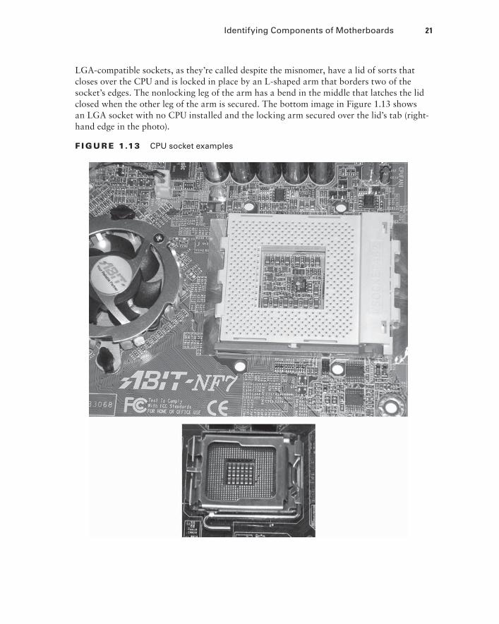
The processor slot is another method of connecting a processor to a motherboard, but one into which a processor (such as the AMD Athlon or the Intel Pentium II or Pentium III) on a special expansion card is inserted (the slot shown in Figure 1.14). Newer, more com-plex processors, such as the Intel Itanium, use a similar packaging, known as a Pin Array Cartridge (PAC), which uses a complex mechanism for inserting the large rectangular PAC CPU carrier. The connector that receives a PAC works on the Very Low Insertion Force (VLIF) principle. To see which socket type is used for which processors, examine Table 1.1.
F I GU R E 1.14 A Slot 1 connection slot
TA B LE 1.1 Socket/Slot Types and the Processors They Support
Socket/Slot Processors
Slot 1 Pentium II, Pentium III, Celeron, and all SECC and SECC2
Slot 2 Pentium II Xeon, Pentium III Xeon (server)—replaced by Socket 370
Slot A Early AMD Athlon, physically the same as Slot 1, but not electrically—replaced by Socket A
Sockets 1, 2, 3, 6 486 and Pentium OverDrive
86498book.indb 22 7/22/09 5:37:29 AM
Identifying Components of Motherboards 23
TA B LE 1.1 Socket/Slot Types and the Processors They Support (continued)
Socket/Slot Processors
Socket 4 Pentium 60/66, Pentium 60/66 OverDrive
Socket 5 Pentium 75-133, Pentium 75+ OverDrive, AMD K5
Socket 7 Pentium 75-200, Pentium 75+ OverDrive, Pentium MMX, AMD K6
Super Socket 7 AMD K6-2, K6-III
Socket 8 Oddly combined SPGA/PGA format for Pentium Pro—replaced by Slot 1 with the introduction of Pentium II
Socket 370 Plastic PGA (PPGA) processors, including Pentium III and Celeron
Socket 423 Early Pentium 4
Socket A (Socket 462) AMD Athlon, Athlon XP, Athlon XP-M, Athlon MP, Thunderbird, Duron, Sempron
Socket 478 Pentium 4, Pentium 4 Extreme Edition, Celeron
Socket 479 Laptop Pentium M, Celeron M
Socket 563 AMD low-power mobile Athlon XP-M
Socket 603 Intel Xeon
Socket 604 Intel Xeon with Micro Flip-chip PGA (FCPGA) package
Socket 754 Athlon 64, Sempron, Turion 64
Socket P For 478-pin Micro FCPGA mobile packages, such as Core 2 Duo, Celeron M, and Pentium Dual-Core
Socket T (LGA 775) Desktop processors, such as Pentium 4, Pentium D, Celeron D, Pentium Extreme Edition, Core 2 Duo, Core 2 Extreme, Core 2 Quad
Socket J (LGA 771) Server version of LGA 775, Dual-Core Xeon
Socket B (LGA 1366) Intel Core i7
Socket 939 Athlon 64, Athlon 64 FX, Athlon 64 X2, Opteron 100-series
Socket 940 Intended for AMD servers, Athlon 64 FX (FX-51), Opteron
86498book.indb 23 7/22/09 5:37:29 AM
24 Chapter 1 Personal Computer System Components
TA B LE 1.1 Socket/Slot Types and the Processors They Support (continued)
Socket/Slot Processors
Socket F (Socket 1207) Replaces Socket 940 when used with Opteron multiprocessor systems—LGA packaging
Socket AM2 AMD single-processor systems, 940 pins (not same as server-based Socket 940), replaces Socket 754 and Socket 939
Socket AM3 DDR3 capable for Phenom series, Athlon X2, Sempron LE, Opteron (single-CPU servers)
Socket S1 AMD-based mobile platforms, replaces Socket 754 in the mobile sector
PAC418 Itanium (instead of proposed Slot 3/Slot M)
PAC611 Itanium 2
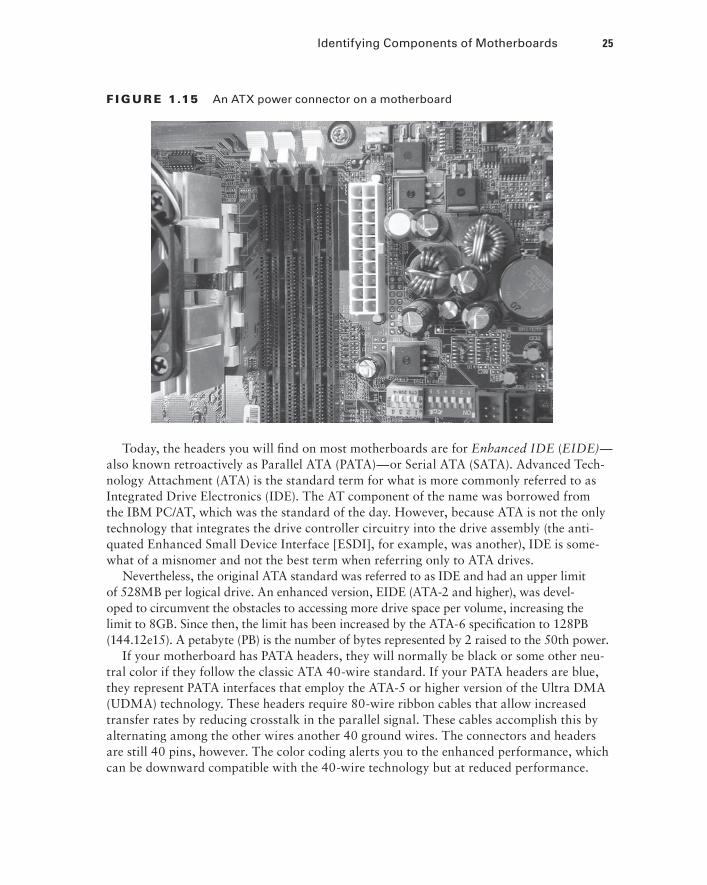
Power Connectors
In addition to these sockets and slots on the motherboard, a special connector (the 20-pin block connector shown in Figure 1.15) allows the motherboard to be connected to the power supply to receive power. This connector is where the ATX power connector (men-tioned in Chapter 2 in the section “Identifying Purposes and Characteristics of Power Sup-plies”) plugs in.
Onboard Floppy and Hard Disk Connectors
Almost every computer made today uses some type of disk drive to store data and pro-grams until they are needed. All drives need some form of connection to the motherboard so the computer can “talk” to the disk drive. Regardless of whether the connection is built into the motherboard (onboard)—it could reside on an adapter card (off-board)—the standard for the attachment is based on the drive’s requirements. These connections are known as drive interfaces, and there are two main types: floppy drive interfaces and hard disk drive interfaces. Floppy drive interfaces allow floppy disk drives (FDDs) to be con-nected to the motherboard, and similarly, hard disk drive interfaces do the same for hard disks and optical drives, among others. The interfaces consist of circuitry and a port, or header. Most motherboards produced today include both the floppy disk and non-SCSI hard disk interfaces on the motherboard. Server motherboards often include SCSI headers and circuitry instead.
86498book.indb 24 7/22/09 5:37:29 AM
Identifying Components of Motherboards 25
F I GU R E 1.15 An ATX power connector on a motherboard
Today, the headers you will find on most motherboards are for Enhanced IDE (EIDE)—also known retroactively as Parallel ATA (PATA)—or Serial ATA (SATA). Advanced Tech-nology Attachment (ATA) is the standard term for what is more commonly referred to as Integrated Drive Electronics (IDE). The AT component of the name was borrowed from the IBM PC/AT, which was the standard of the day. However, because ATA is not the only technology that integrates the drive controller circuitry into the drive assembly (the anti-quated Enhanced Small Device Interface [ESDI], for example, was another), IDE is some-what of a misnomer and not the best term when referring only to ATA drives.
Nevertheless, the original ATA standard was referred to as IDE and had an upper limit of 528MB per logical drive. An enhanced version, EIDE (ATA-2 and higher), was devel-oped to circumvent the obstacles to accessing more drive space per volume, increasing the limit to 8GB. Since then, the limit has been increased by the ATA-6 specification to 128PB (144.12e15). A petabyte (PB) is the number of bytes represented by 2 raised to the 50th power.
If your motherboard has PATA headers, they will normally be black or some other neu-tral color if they follow the classic ATA 40-wire standard. If your PATA headers are blue, they represent PATA interfaces that employ the ATA-5 or higher version of the Ultra DMA (UDMA) technology. These headers require 80-wire ribbon cables that allow increased transfer rates by reducing crosstalk in the parallel signal. These cables accomplish this by alternating among the other wires another 40 ground wires. The connectors and headers are still 40 pins, however. The color coding alerts you to the enhanced performance, which can be downward compatible with the 40-wire technology but at reduced performance.
86498book.indb 25 7/22/09 5:37:30 AM
26 Chapter 1 Personal Computer System Components
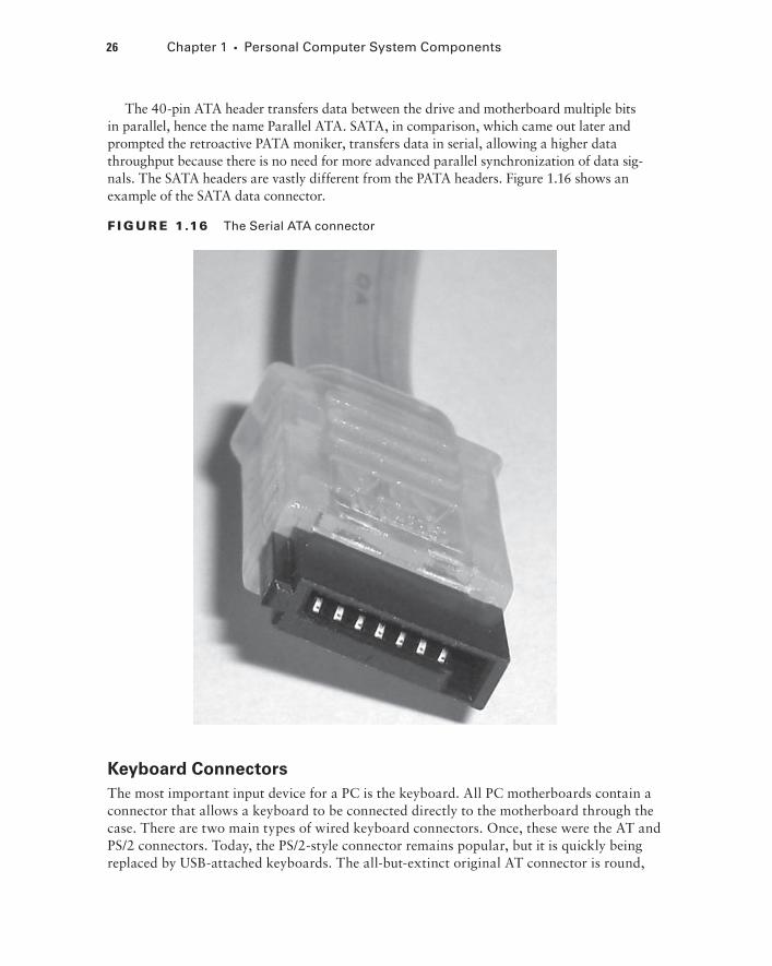
The 40-pin ATA header transfers data between the drive and motherboard multiple bits in parallel, hence the name Parallel ATA. SATA, in comparison, which came out later and prompted the retroactive PATA moniker, transfers data in serial, allowing a higher data throughput because there is no need for more advanced parallel synchronization of data sig-nals. The SATA headers are vastly different from the PATA headers. Figure 1.16 shows an example of the SATA data connector.
F I GU R E 1.16 The Serial ATA connector
Keyboard Connectors
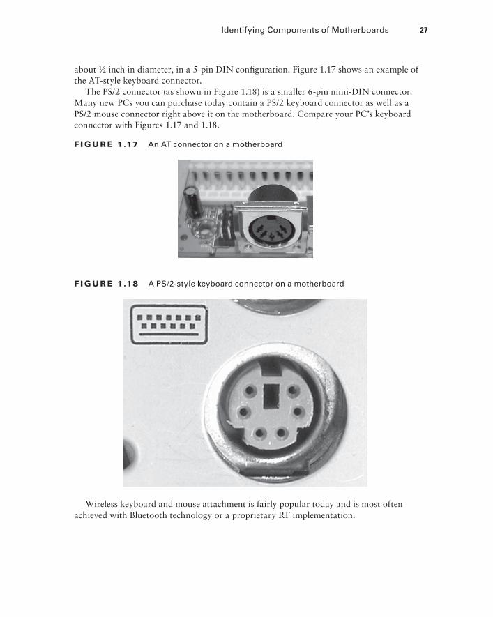
The most important input device for a PC is the keyboard. All PC motherboards contain a connector that allows a keyboard to be connected directly to the motherboard through the case. There are two main types of wired keyboard connectors. Once, these were the AT and PS/2 connectors. Today, the PS/2-style connector remains popular, but it is quickly being replaced by USB-attached keyboards. The all-but-extinct original AT connector is round,
86498book.indb 26 7/22/09 5:37:30 AM
Identifying Components of Motherboards 27
about ½ inch in diameter, in a 5-pin DIN configuration. Figure 1.17 shows an example of the AT-style keyboard connector.
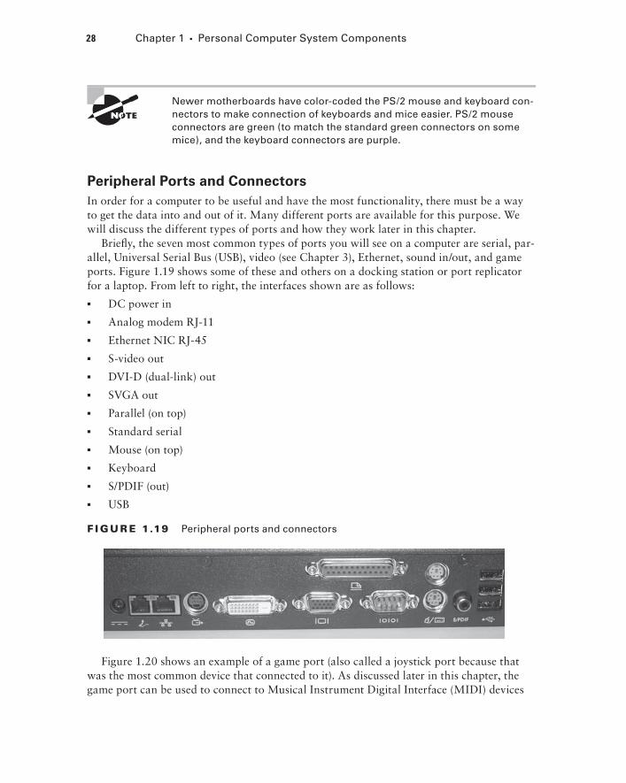
The PS/2 connector (as shown in Figure 1.18) is a smaller 6-pin mini-DIN connector. Many new PCs you can purchase today contain a PS/2 keyboard connector as well as a PS/2 mouse connector right above it on the motherboard. Compare your PC’s keyboard connector with Figures 1.17 and 1.18.
F I GU R E 1.17 An AT connector on a motherboard
F I GU R E 1.18 A PS/2-style keyboard connector on a motherboard
Wireless keyboard and mouse attachment is fairly popular today and is most often achieved with Bluetooth technology or a proprietary RF implementation.
86498book.indb 27 7/22/09 5:37:31 AM
28 Chapter 1 Personal Computer System Components
Newer motherboards have color-coded the PS/2 mouse and keyboard con-nectors to make connection of keyboards and mice easier. PS/2 mouse connectors are green (to match the standard green connectors on some mice), and the keyboard connectors are purple.
Peripheral Ports and Connectors
In order for a computer to be useful and have the most functionality, there must be a way to get the data into and out of it. Many different ports are available for this purpose. We will discuss the different types of ports and how they work later in this chapter.
Briefly, the seven most common types of ports you will see on a computer are serial, par-allel, Universal Serial Bus (USB), video (see Chapter 3), Ethernet, sound in/out, and game ports. Figure 1.19 shows some of these and others on a docking station or port replicator for a laptop. From left to right, the interfaces shown are as follows:
DC power in
Analog modem RJ-11
Ethernet NIC RJ-45
S-video out
DVI-D (dual-link) out
SVGA out
Parallel (on top)
Standard serial
Mouse (on top)
Keyboard
S/PDIF (out)
USB
F I GU R E 1.19 Peripheral ports and connectors
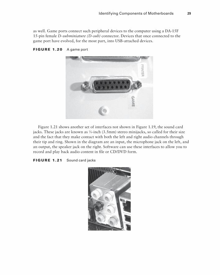
Figure 1.20 shows an example of a game port (also called a joystick port because that was the most common device that connected to it). As discussed later in this chapter, the game port can be used to connect to Musical Instrument Digital Interface (MIDI) devices
86498book.indb 28 7/22/09 5:37:31 AM
Identifying Components of Motherboards 29
as well. Game ports connect such peripheral devices to the computer using a DA-15F 15-pin female D-subminiature (D-sub) connector. Devices that once connected to the game port have evolved, for the most part, into USB-attached devices.
F I GU R E 1. 20 A game port
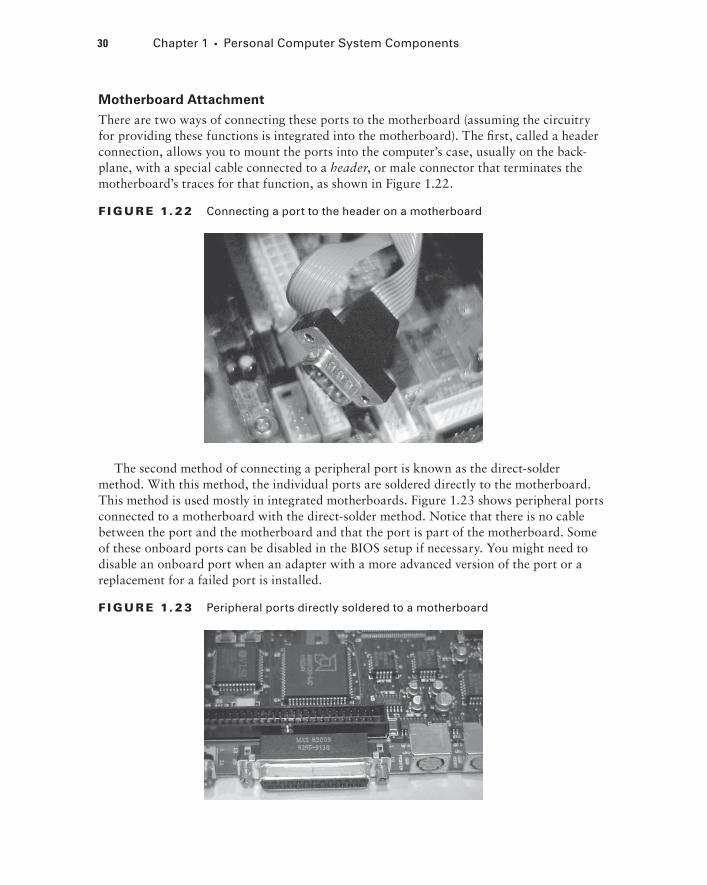
Figure 1.21 shows another set of interfaces not shown in Figure 1.19, the sound card jacks. These jacks are known as 1⁄8-inch (3.5mm) stereo minijacks, so called for their size and the fact that they make contact with both the left and right audio channels through their tip and ring. Shown in the diagram are an input, the microphone jack on the left, and an output, the speaker jack on the right. Software can use these interfaces to allow you to record and play back audio content in file or CD/DVD form.
F I GU R E 1. 21 Sound card jacks
86498book.indb 29 7/22/09 5:37:31 AM
30 Chapter 1 Personal Computer System Components
Motherboard Attachment
There are two ways of connecting these ports to the motherboard (assuming the circuitry for providing these functions is integrated into the motherboard). The first, called a header connection, allows you to mount the ports into the computer’s case, usually on the back-plane, with a special cable connected to a header, or male connector that terminates the motherboard’s traces for that function, as shown in Figure 1.22.
F I GU R E 1. 22 Connecting a port to the header on a motherboard
The second method of connecting a peripheral port is known as the direct-solder method. With this method, the individual ports are soldered directly to the motherboard. This method is used mostly in integrated motherboards. Figure 1.23 shows peripheral ports connected to a motherboard with the direct-solder method. Notice that there is no cable between the port and the motherboard and that the port is part of the motherboard. Some of these onboard ports can be disabled in the BIOS setup if necessary. You might need to disable an onboard port when an adapter with a more advanced version of the port or a replacement for a failed port is installed.
F I GU R E 1. 23 Peripheral ports directly soldered to a motherboard
86498book.indb 30 7/22/09 5:37:32 AM
Identifying Components of Motherboards 31
BIOS and POST
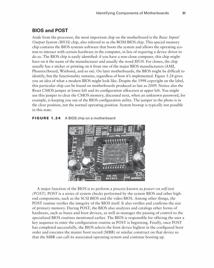
Aside from the processor, the most important chip on the motherboard is the Basic Input/Output System (BIOS) chip, also referred to as the ROM BIOS chip. This special memory chip contains the BIOS systems software that boots the system and allows the operating sys-tem to interact with certain hardware in the computer, in lieu of requiring a device driver to do so. The BIOS chip is easily identified: if you have a non-clone computer, this chip might have on it the name of the manufacturer and usually the word BIOS. For clones, the chip usually has a sticker or printing on it from one of the major BIOS manufacturers (AMI, Phoenix/Award, Winbond, and so on). On later motherboards, the BIOS might be difficult to identify, but the functionality remains, regardless of how it’s implemented. Figure 1.24 gives you an idea of what a modern BIOS might look like. Despite the 1998 copyright on the label, this particular chip can be found on motherboards produced as late as 2009. Notice also the Reset CMOS jumper at lower left and its configuration silkscreen at upper left. You might use this jumper to clear the CMOS memory, discussed next, when an unknown password, for example, is keeping you out of the BIOS configuration utility. The jumper in the photo is in the clear position, not the normal operating position. System bootup is typically not possible in this state.
F I GU R E 1. 24 A BIOS chip on a motherboard
A major function of the BIOS is to perform a process known as power-on self-test (POST). POST is a series of system checks performed by the system BIOS and other high-end components, such as the SCSI BIOS and the video BIOS. Among other things, the POST routine verifies the integrity of the BIOS itself. It also verifies and confirms the size of primary memory. During POST, the BIOS also analyzes and catalogs other forms of hardware, such as buses and boot devices, as well as manages the passing of control to the specialized BIOS routines mentioned earlier. The BIOS is responsible for offering the user a key sequence to enter the configuration routine as POST is beginning. Finally, once POST has completed successfully, the BIOS selects the boot device highest in the configured boot order and executes the master boot record (MBR) or similar construct on that device so that the MBR can call its associated operating system and continue booting up.
86498book.indb 31 7/22/09 5:37:32 AM
32 Chapter 1 Personal Computer System Components
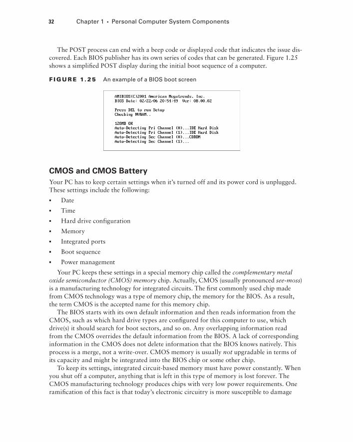
The POST process can end with a beep code or displayed code that indicates the issue dis-covered. Each BIOS publisher has its own series of codes that can be generated. Figure 1.25 shows a simplified POST display during the initial boot sequence of a computer.
F I GU R E 1. 25 An example of a BIOS boot screen
CMOS and CMOS Battery
Your PC has to keep certain settings when it’s turned off and its power cord is unplugged. These settings include the following:
Date
Time
Hard drive configuration
Memory
Integrated ports
Boot sequence
Power management
Your PC keeps these settings in a special memory chip called the complementary metal oxide semiconductor (CMOS) memory chip. Actually, CMOS (usually pronounced see-moss) is a manufacturing technology for integrated circuits. The first commonly used chip made from CMOS technology was a type of memory chip, the memory for the BIOS. As a result, the term CMOS is the accepted name for this memory chip.
The BIOS starts with its own default information and then reads information from the CMOS, such as which hard drive types are configured for this computer to use, which drive(s) it should search for boot sectors, and so on. Any overlapping information read from the CMOS overrides the default information from the BIOS. A lack of corresponding information in the CMOS does not delete information that the BIOS knows natively. This process is a merge, not a write-over. CMOS memory is usually not upgradable in terms of its capacity and might be integrated into the BIOS chip or some other chip.
To keep its settings, integrated circuit-based memory must have power constantly. When you shut off a computer, anything that is left in this type of memory is lost forever. The CMOS manufacturing technology produces chips with very low power requirements. One ramification of this fact is that today’s electronic circuitry is more susceptible to damage
86498book.indb 32 7/22/09 5:37:32 AM

Identifying Components of Motherboards 33
from electrostatic discharge (ESD). Another ramification is that it doesn’t take much of a power source to keep CMOS chips from losing their contents.
To prevent CMOS from losing its rather important information, motherboard manu-facturers include a small battery called the CMOS battery to power the CMOS memory. The batteries come in different shapes and sizes, but they all perform the same function. Most CMOS batteries look like large watch batteries or small, cylindrical batteries. Today’s CMOS batteries are most often of a long-life, nonrechargeable lithium chemistry.
Jumpers and DIP Switches
The last components of the motherboard we will discuss in this section are jumpers and DIP switches. These two devices are used to configure various hardware options on the motherboard. For example, some motherboards support processors that use different core (internal) and I/O (external) voltages. You must set the motherboard to provide the cor-rect voltage for the processor it is using. You do so by changing a setting on the mother-board with either a jumper or a DIP switch. Figure 1.26 shows both a jumper set and DIP switches. Motherboards often have either several jumpers or one bank of DIP switches. Individual jumpers are often labeled with the moniker JPx (where x is a unique number for the jumper).
F I GU R E 1. 26 Jumpers and DIP switches
Jumper Rocker-type DIP switch Slide-type DIP switch
Many of the motherboard settings that were set using jumpers and DIP switches are now either automatically detected or set manually in the BIOS setup program.
Firmware
Firmware is the name given to any software that is encoded in hardware, usually a read-only memory (ROM) chip, and can be run without extra instructions from the operating system. Most computers and large printers use firmware in some sense. The best example of firmware is a computer’s BIOS routine, which is burned in to a chip. Also, some expansion cards, such as small computer system interface (SCSI) cards and graphics adapters, use their own firmware utilities for setting up peripherals.
86498book.indb 33 7/22/09 5:37:33 AM
34 Chapter 1 Personal Computer System Components
Identifying Purposes and Characteristics of ProcessorsNow that you’ve learned the basics of the motherboard, you need to learn about the most important component on the motherboard: the CPU. The role of the CPU, or central pro-cessing unit, is to control and direct all the activities of the computer using both external and internal buses. It is a processor chip consisting of an array of millions of transistors. Intel and Advanced Micro Devices (AMD) are the two largest PC-compatible CPU manu-facturers. Their chips were featured earlier in Table 1.1 during the discussion of the sockets and slots in which they fit.
The term chip has grown to describe the entire package that a technician might install in a socket. However, the word originally denoted the silicon wafer that is generally hidden within the carrier that you actually see. The external pins you see are structures that can withstand insertion into a socket and that are carefully threaded from the wafer’s minuscule con-tacts. Just imagine how fragile the structures must be that you don’t see.
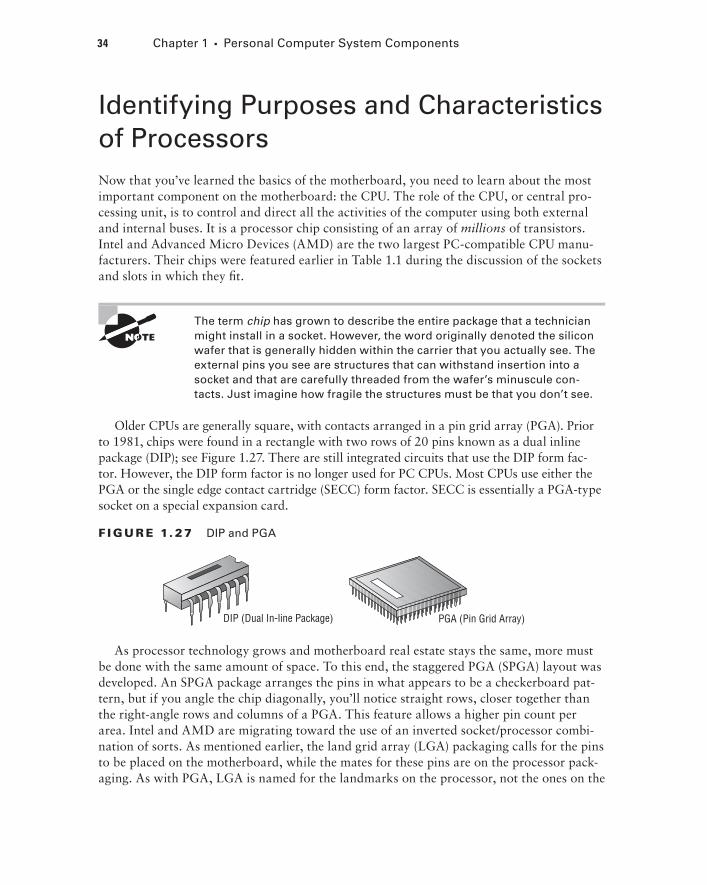
Older CPUs are generally square, with contacts arranged in a pin grid array (PGA). Prior to 1981, chips were found in a rectangle with two rows of 20 pins known as a dual inline package (DIP); see Figure 1.27. There are still integrated circuits that use the DIP form fac-tor. However, the DIP form factor is no longer used for PC CPUs. Most CPUs use either the PGA or the single edge contact cartridge (SECC) form factor. SECC is essentially a PGA-type socket on a special expansion card.
F I GU R E 1. 27 DIP and PGA
DIP (Dual In-line Package) PGA (Pin Grid Array)
As processor technology grows and motherboard real estate stays the same, more must be done with the same amount of space. To this end, the staggered PGA (SPGA) layout was developed. An SPGA package arranges the pins in what appears to be a checkerboard pat-tern, but if you angle the chip diagonally, you’ll notice straight rows, closer together than the right-angle rows and columns of a PGA. This feature allows a higher pin count per area. Intel and AMD are migrating toward the use of an inverted socket/processor combi-nation of sorts. As mentioned earlier, the land grid array (LGA) packaging calls for the pins to be placed on the motherboard, while the mates for these pins are on the processor pack-aging. As with PGA, LGA is named for the landmarks on the processor, not the ones on the
86498book.indb 34 7/22/09 5:37:37 AM
Identifying Purposes and Characteristics of Processors 35
motherboard. As a result, the grid of metallic contact points, called lands, on the bottom of the CPU gives this format its name.
This discussion only scratches the surface of the topic surrounding chip packaging and carriers. For more information on the various packaging for chips, start with .
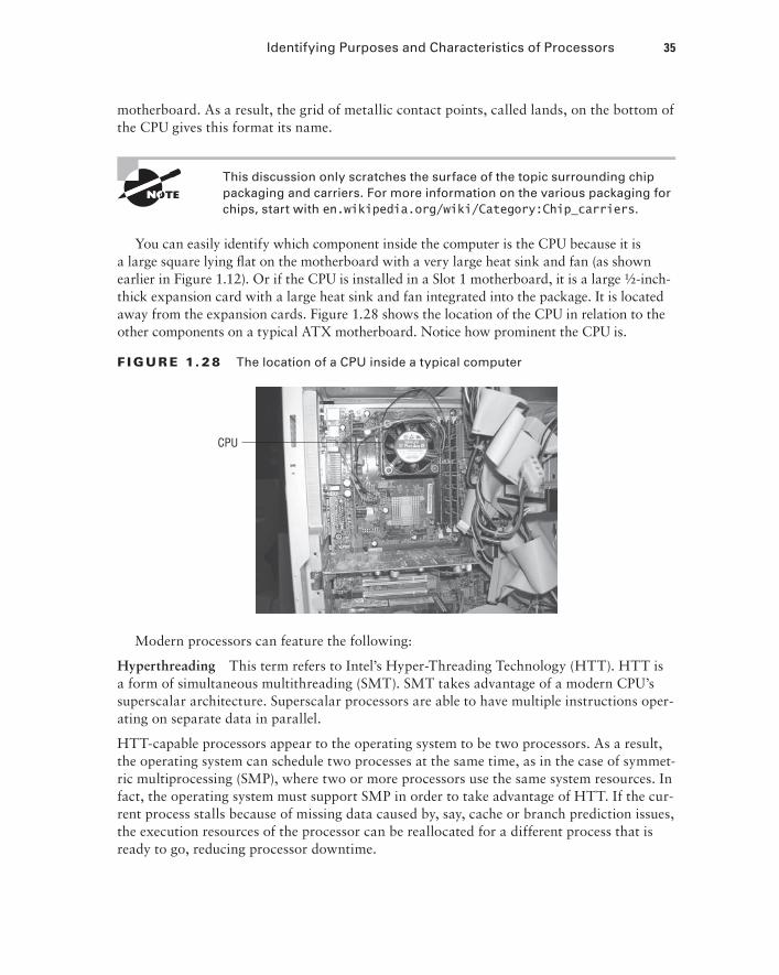
You can easily identify which component inside the computer is the CPU because it is a large square lying flat on the motherboard with a very large heat sink and fan (as shown earlier in Figure 1.12). Or if the CPU is installed in a Slot 1 motherboard, it is a large ½-inch-thick expansion card with a large heat sink and fan integrated into the package. It is located away from the expansion cards. Figure 1.28 shows the location of the CPU in relation to the other components on a typical ATX motherboard. Notice how prominent the CPU is.
F I GU R E 1. 28 The location of a CPU inside a typical computer
CPU
Modern processors can feature the following:
Hyperthreading This term refers to Intel’s Hyper-Threading Technology (HTT). HTT is a form of simultaneous multithreading (SMT). SMT takes advantage of a modern CPU’s superscalar architecture. Superscalar processors are able to have multiple instructions oper-ating on separate data in parallel.
HTT-capable processors appear to the operating system to be two processors. As a result, the operating system can schedule two processes at the same time, as in the case of symmet-ric multiprocessing (SMP), where two or more processors use the same system resources. In fact, the operating system must support SMP in order to take advantage of HTT. If the cur-rent process stalls because of missing data caused by, say, cache or branch prediction issues, the execution resources of the processor can be reallocated for a different process that is ready to go, reducing processor downtime.
86498book.indb 35 7/22/09 5:37:38 AM
36 Chapter 1 Personal Computer System Components
Which CPU Do You Have?
The surest way to determine which CPU your computer is using is to open the case and view the numbers stamped on the CPU, which today requires removal of the active heat sink. However, you may be able to get an idea without opening the case and removing the heat sink and fan, because many manufacturers indicate the type of processor by placing a very obvious sticker somewhere on the case indicating the processor type. Failing this, you can always go to the manufacturer’s website and look up the information on the model of computer you have.
If you have a no-name clone, there is always the System Properties pages, found by right-clicking My Computer (Computer in Windows Vista) and selecting Properties. The Gen-eral tab, which is the default, contains such information. Even more detailed information can be found by running the System Information utility from Tools Advanced System Information in the Windows XP Help and Support Center or by entering in the Start Run dialog box for all modern Microsoft desktop operating systems.
Another way to determine a computer’s CPU is to save your work, exit any open programs, and restart the computer. Watch closely as the computer returns to its normal state. You should see a notation that tells you what chip you are using.
Multicore A processor that exhibits a multicore architecture has multiple completely separate processor dies in the same package. The operating system and applications see multiple processors in the same way that they see multiple processors in separate sockets. As with HTT, the operating system must support SMP to benefit from the separate proces-sors. In addition, SMP is not an enhancement if the applications run on the SMP system are not written for parallel processing. Dual-core and quad-core processors are common specific cases for the multicore technology.
Don’t be confused by Intel’s Core 2 labeling. The numeric component does not imply there are two cores. There was a Core series of 32-bit mobile processors that featured one (Solo) or two (Duo) processing cores on a single die (silicon wafer). The same dual-core die was used for both classes of Core CPU. The second core was disabled for Core Solo processors.
The 64-bit Core 2 product line can be thought of as a second generation of the Core series. Core 2, by the way, reunited Intel mobile and desktop computing—the Pentium 4 family had a separate Pentium M for mobile computing. Intel describes and markets the microcode of certain processors as “Core microarchitecture.” As confusing as it may sound, the Core 2 processors are based on the Core microarchitecture; the Core processors are not. Core 2
86498book.indb 36 7/22/09 5:37:39 AM
Identifying Purposes and Characteristics of Processors 37
processors come in Solo (mobile only), Duo, and four-core (Quad) implementations. Solo and Duo processors have a single die; Quad processors have two Duo dies. A more capable Extreme version exists for the Duo and Quad models.
Processors, such as certain models of AMD’s Phenom series, can contain an odd number of multiple cores as well. The triple-core processor, which obviously contains three cores, is the most common implementation of multiple odd cores.
Throttling CPU throttling allows reducing the operating frequency of the CPU during times of less demand or during battery operation. CPU throttling is very common in pro-cessors for mobile devices, where heat generation and system-battery drain are key issues of full power usage. You might discover throttling in action when you use a utility that reports a lower CPU clock frequency than expected. If the load on the system does not require full-throttle operation, there is no need to push such a limit.
Microcode and multimedia extensions Microcode is the set of instructions (known as an instruction set) that make up the various microprograms that the processor executes while carrying out its various duties. The Multimedia Extensions (MMX) microcode is a specialized example of a separate microprogram that carries out a particular set of functions. Microcode is at a much lower level than the code that makes up application programs. Each instruction in an application will end up being represented by many microinstructions, on average. The MMX instruction set is incorporated into most modern CPUs from Intel and others. MMX came about as a way to take much of the multimedia processing off the CPU’s hands, leaving the processor to other tasks. Think of it as sort of a coprocessor for multimedia, much like the floating-point unit (FPU) is a math coprocessor.
Cache As mentioned in the “Memory Slots and Cache” section earlier in this chapter, cache is a very fast chip memory that is used to hold data and instructions that are most likely to be requested next by the CPU. The cache located on the CPU die is known as L1 cache and is generally of a smaller capacity in comparison to L2 cache, which is located on the mother-board or off-die in the same CPU packaging. When the CPU requires outside information, it believes it requests that information from RAM. The cache controller, however, intercepts the request and consults its tag RAM to discover if the requested information is already cached, either at L1 or L2. If not, a cache miss is recorded and the information is brought back from the much slower RAM, but this new information sticks to the various levels of cache on its way to the CPU from RAM.
Speed The speed of the processor is generally described in clock frequency (MHz or GHz). There can be a discrepancy between the advertised frequency and the frequency the CPU uses to latch data and instructions through the pipeline. This disagreement between the numbers comes from the fact that the CPU is capable of splitting the clock signal it receives from the external oscillator that drives the frontside bus into multiple regular sig-nals for its own internal use. In fact, you might be able to purchase a number of processors rated for different (internal) speeds that are all compatible with a single motherboard that has a frontside bus rated, for instance, at 800MHz.
86498book.indb 37 7/22/09 5:37:39 AM
38 Chapter 1 Personal Computer System Components
Matching System Components
In a world of clock doubling, tripling, quadrupling, and so forth, it becomes increasingly important to pay attention to what you are buying when you purchase CPUs, memory, and motherboards a la carte. The only well-known relationship that exists among these components is the speed of the FSB (in MHz) and the throughput of the memory (in MBps). Because 8 bytes are transferred in parallel by a processor with a 64-bit (64 bits = 8 bytes) system data bus, you have to know the FSB rating before you choose the RAM for any particular modern motherboard. For example, a FSB of 800MHz requires memory rated at a throughput of 6400MBps (800 million cycles per second 8 bytes per cycle).
Matching CPUs with motherboards or CPUs with memory requires consulting the docu-mentation or packaging of the components. Generally, the CPU gets selected first. Once you know the CPU you want, the motherboard tends to come next. You must choose a motherboard that features a slot or socket compatible with your chosen CPU. The FSB used on the selected motherboard dictates the RAM you should purchase.
32- and 64-bit processors The set of data lines between the CPU and the primary memory of the system can be 32 or 64 bits wide, among other widths. The wider the bus, the more data that can be processed per unit of time, and hence, the more work that can be performed. Internal registers in the CPU might be only 32 bits wide, but with a 64-bit system bus, two separate pipelines can receive information simultaneously. For true 64-bit CPUs, which have 64-bit internal registers and can run x64 versions of Microsoft operating systems, the exter-nal system data bus should be 64 bits wide or some larger multiple thereof.
Identifying Purposes and Characteristics of Memory“More memory, more memory, I don’t have enough memory!” Today, memory is one of the most popular, easy, and inexpensive ways to upgrade a computer. As the computer’s CPU works, it stores data and instructions in the computer’s memory. Contrary to what you might expect from an inexpensive solution, memory upgrades tend to afford the greatest performance increase as well, up to a point. Motherboards have memory limits; operating systems have memory limits; CPUs have memory limits.
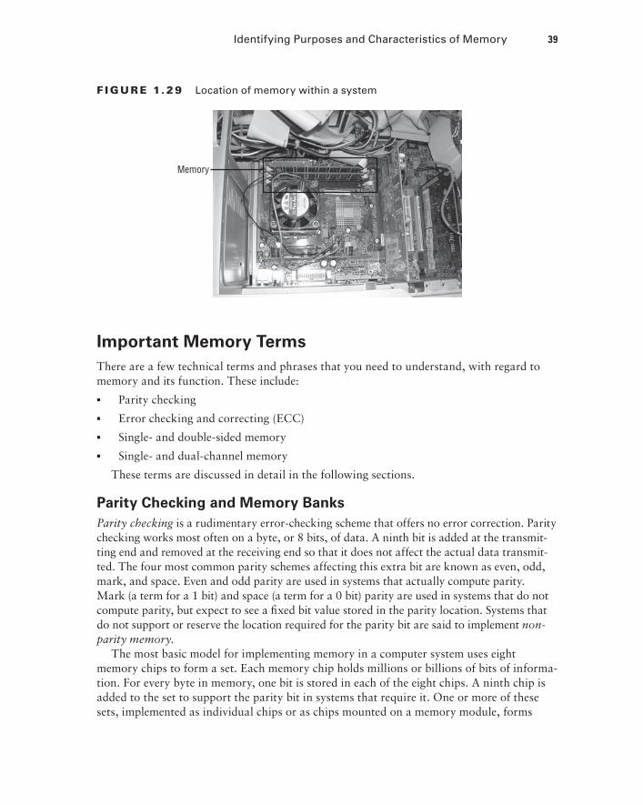
To identify memory within a computer, look for several thin rows of small circuit boards sitting vertically, packed tightly together near the processor. In situations where only one memory stick is installed, it will be that stick and a few empty slots that are tightly packed together. Figure 1.29 shows where memory is located in a system.
86498book.indb 38 7/22/09 5:37:39 AM
Identifying Purposes and Characteristics of Memory 39
F I GU R E 1. 29 Location of memory within a system
Memory
Important Memory Terms
There are a few technical terms and phrases that you need to understand, with regard to memory and its function. These include:
Parity checking
Error checking and correcting (ECC)
Single- and double-sided memory
Single- and dual-channel memory
These terms are discussed in detail in the following sections.
Parity Checking and Memory Banks
Parity checking is a rudimentary error-checking scheme that offers no error correction. Parity checking works most often on a byte, or 8 bits, of data. A ninth bit is added at the transmit-ting end and removed at the receiving end so that it does not affect the actual data transmit-ted. The four most common parity schemes affecting this extra bit are known as even, odd, mark, and space. Even and odd parity are used in systems that actually compute parity. Mark (a term for a 1 bit) and space (a term for a 0 bit) parity are used in systems that do not compute parity, but expect to see a fixed bit value stored in the parity location. Systems that do not support or reserve the location required for the parity bit are said to implement non-parity memory.
The most basic model for implementing memory in a computer system uses eight memory chips to form a set. Each memory chip holds millions or billions of bits of informa-tion. For every byte in memory, one bit is stored in each of the eight chips. A ninth chip is added to the set to support the parity bit in systems that require it. One or more of these sets, implemented as individual chips or as chips mounted on a memory module, forms
86498book.indb 39 7/22/09 5:37:41 AM
40 Chapter 1 Personal Computer System Components
a memory bank. A bank of memory is required for the computer system to electrically recognize that memory or additional memory has been installed. The width of the system data bus, the external bus of the processor, dictates how many memory chips or modules are required to satisfy a bank. For example, one 32-bit, 72-pin SIMM satisfies a bank for a 32-bit CPU, such as a 386 or 486 processor. Two such modules are required to satisfy a bank for a 64-bit processor, a Pentium, for instance. However, only a single 64-bit, 168-pin DIMM is required to satisfy the same Pentium processor. For those modules that have fewer than eight or nine chips mounted on them, more than one bit for every byte is being handled by some of the chips. For example, if you see three chips mounted, the two larger chips probably handle 4 bits, a nybble, from each byte stored, and the third, smaller chip probably handles the single parity bit for each byte.
Even and odd parity schemes operate on each byte in the set of memory chips. In each case, the number of bits set to a value of 1 is counted up. If there are an even number of 1-bits in the byte (0, 2, 4, 6, or 8), even parity stores a 0 in the ninth bit, the parity bit; otherwise, it stores a 1 to even up the count. Odd parity does just the opposite, storing a 1 in the parity bit to make an even number of 1s odd and a 0 to keep an odd number of 1s odd. You can see that this is effective only for determining if there was a blatant error in the set of bits received, but there is no indication as to where the error is and how to fix it. Furthermore, the total 1-bit count is not important, only whether it’s even or odd. Therefore, in either the even or odd scheme, if an even number of bits is altered in the same byte during transmission, the error goes undetected because flipping 2, 4, 6, or all 8 bits results in an even number of 1s remaining even and an odd number of 1s remaining odd.
Mark and space parity are used in systems that want to see 9 bits for every byte trans-mitted but don’t compute the parity bit’s value based on the bits in the byte. Mark parity always uses a 1 in the parity bit, and space parity always uses a 0. These schemes offer less error detection capability than the even and odd schemes because only changes in the parity bit can be detected. Again, parity checking is not error correction; it’s error detection only, and not the best form of error detection at that. Nevertheless, finding an error can lock up the entire system and display a memory parity error. Enough of these errors and you need to replace the memory.
In the early days of personal computing, almost all memory was parity-based. Compaq was one of the first manufacturers to employ non-parity RAM in their mainstream systems. As quality has increased over the years, parity checking in the RAM subsystem has become rarer. As noted earlier, if parity checking is not supported, there will generally be fewer chips per module, usually one less per column of RAM.
Error Checking and Correction
The next step in the evolution of memory error detection is known as error checking and cor-recting (ECC). If memory supports ECC, check bits are generated and stored with the data. An algorithm is performed on the data and its check bits whenever the memory is accessed. If the result of the algorithm is all zeros, then the data is deemed valid and processing continues. ECC can detect single- and double-bit errors and actually correct single-bit errors.
In this section, we’ll outline the major types of computer memory as well as the methods of implementing, or packaging, such memory.
86498book.indb 40 7/22/09 5:37:41 AM

Identifying Purposes and Characteristics of Memory 41
Single- and Double-Sided Memory
Ask just about anyone who doesn’t manufacture memory for a living what the terms single-sided memory and double-sided memory mean, and you’ll be treated to a blank stare or a short diatribe on how some memory modules have chips on one side, while others have chips on both sides. In fact, these terms have nothing to do with the physical attachment of chips to the modules. Either style can have chips on one or both sides of the module.
Double-sided memory is essentially treated by the system as two separate memory modules. Motherboards that support such memory have memory controllers that must switch between the two “sides” of the modules and, at any particular moment, can only access the side they have switched to. For the state-of-the-art memory at the time, double-sided memory allows more memory to be inserted into a computer using half the physical space of single-sided memory, which requires no switching by the memory controller.
Single- and Dual-Channel Memory
Standard memory controllers manage access to memory in chunks of the same size as the FSB’s data width. This is considered communicating over a single channel. Most modern processors have a 64-bit system data bus. This means a standard memory controller can transfer exactly 64 bits of information at a time. Communicating over a single channel is a bottleneck in an environment where the CPU and memory can both operate faster than the conduit between them. Up to a point, every channel added in parallel between the CPU and RAM serves to ease this constriction.
Memory controllers that support or require dual-channel memory implementation were developed in an effort to alleviate the bottleneck between the CPU and RAM. Dual-channel memory is the memory controller’s coordination of two memory banks to work as a synchro-nized set during communication with the CPU, doubling the specified system bus width, from the memory’s perspective. Because today’s processors largely have 64-bit external data buses, and because one stick of memory satisfies this bus width, there is a 1:1 ratio between banks and modules. This means that implementing dual-channel memory in today’s most popular computer systems generally requires that pairs of memory modules be installed at a time. Note, however, that it’s the motherboard, not the memory that implements dual-channel memory (more on this in a moment). Single-channel memory, in contrast, is the classic mem-ory model that dictates only that a complete bank be satisfied whenever memory is initially installed or added. One bank supplies only half the width of the effective bus created by dual-channel support, which, by definition, pairs two banks at a time.
Because of the special tricks that are played with memory subsystems to improve over-all system performance, care must be taken during the installation of disparate memory modules. In the worst case, the computer will cease to function when modules of different speeds, different capacities, or different numbers of sides are placed together in slots of the same channel. If all of these parameters are identical, there should be no problem with pairing modules. Nevertheless, problems could still occur when modules from two differ-ent manufacturers or certain unsupported manufacturers are installed, all other param-eters being the same. Technical support or documentation from the manufacturer of your mother board should be able to help with such issues.
86498book.indb 41 7/22/09 5:37:41 AM
42 Chapter 1 Personal Computer System Components
Although it’s not the make-up of the memory that leads to dual-channel support, but instead the technology on which the motherboard is based, some memory manufacturers still package and sell pairs of memory modules in an effort to give you peace of mind when you’re buying memory for a system that implements dual-channel memory architecture. Keep in mind, the motherboard memory slots have the distinctive color coding, not the memory modules.
I Can’t Fill All My Memory Slots
As a reminder, most motherboard manufacturers document the quantity and types of mod-ules that their equipment supports. Consult your documentation, whether in print or online, when you have questions about supported memory. Most manufacturers require that slower or single-sided memory be inserted in lower-numbered memory slots than faster or double-sided memory. This is because such a system adapts to the first module it sees, looking at the lower-numbered slots first. Counterintuitively, however, it might be required that you install modules of larger capacity in lower-numbered slots than smaller modules.
Additionally, memory technology continues to advance after each generation of mother-board chipsets is announced. Don’t be surprised when you attempt to install a single mod-ule of the highest available capacity in your motherboard, and the system doesn’t recognize the module, either by itself or with others. That capacity of module might not have been in existence when the motherboard’s chipset was released. Consult the motherboard’s docu-mentation!
One common point of confusion, not related to capacity, when installing memory includes lack of recognition of four modules, when two or three modules work fine, for example. In such a case, let’s say your motherboard’s memory controller supports a total of four modules. Recall that a double-sided module acts like two separate modules. If you are using double-sided memory, your motherboard might limit you to two such modules, comprising four sides (essentially four virtual modules), even though you have four slots on the board. If instead you start with three single-sided modules, when you attempt to install a double-sided module in the fourth slot, you are essentially asking the mother-board to accept five modules, which it cannot.
Types of Memory
Memory comes in many formats. Each one has a particular set of features and characteris-tics, making it best suited for a particular application. Some decisions about the application of the memory type are based on suitability; others are based on affordability to consumers
86498book.indb 42 7/22/09 5:37:41 AM
Identifying Purposes and Characteristics of Memory 43
or marketability to computer manufacturers. The following list gives you an idea of the vast array of memory types and subtypes:
DRAM
Asynchronous DRAM
FPM DRAM
EDO DRAM
BEDO DRAM
Synchronous DRAM
SDR SDRAM
DDR SDRAM
DDR2 SDRAM
DDR3 SDRAM
DRDRAM
SRAM
ROM
Pay particular attention to all synchronous DRAM types. Note that the type of memory does not dictate the packaging of the memory. Conversely, however, you might notice one particular memory packaging holding the same type of memory every time you come across it. Nevertheless, there is no requirement to this end. Let’s detail the intricacies of some of these memory types.
DRAM
DRAM is dynamic random access memory. (This is what most people are talking about when they mention RAM.) When you expand the memory in a computer, you are add-ing DRAM chips. You use DRAM to expand the memory in the computer because it’s a cheaper type of memory. Dynamic RAM chips are cheaper to manufacture than most other types because they are less complex. Dynamic refers to the memory chips’ need for a constant update signal (also called a refresh signal) in order to keep the information that is written there. If this signal is not received every so often, the information will bleed off and cease to exist. Currently, the most popular implementations of DRAM are based on syn-chronous DRAM and include SDR SDRAM, DDR, DDR2, DDR3, and DRDRAM. Before discussing these technologies, let’s take a quick look at the all-but-defunct asynchronous memory types.
Asynchronous DRAM
Asynchronous DRAM is characterized by its independence from the CPU’s external clock. Asynchronous DRAM chips have codes on them that end in a numerical value that is related to (often one tenth of the actual value) the access time of the memory. Access
86498book.indb 43 7/22/09 5:37:42 AM
44 Chapter 1 Personal Computer System Components
time is essentially the difference between the time when the information is requested from memory and the time when the data is returned. Common access times attributed to asynchronous DRAM were in the 40- to 120-nanosecond (ns) vicinity. A lower access time is obviously better for overall performance.
Because asynchronous DRAM is not synchronized to the frontside bus, you would often have to insert wait states through the BIOS setup for a faster CPU to be able to use such memory. These wait states represented intervals that the CPU had to mark time and do nothing while waiting for the memory subsystem to become ready again for subse-quent access.
Common asynchronous DRAM technologies included Fast Page Mode (FPM), Extended Data Out (EDO), and Burst EDO (BEDO). Feel free to investigate the details of these par-ticular technologies, but a thorough discussion of these memory types is not necessary here. The A+ technician should be concerned with synchronous forms of RAM, which are the only types of memory being installed in mainstream computer systems today.
Synchronous DRAM
Synchronous DRAM (SDRAM) shares a common clock signal with the computer’s sys-tem-bus clock, which provides the common signal that all local-bus components use for each step that they perform. This characteristic ties SDRAM to the speed of the FSB and, hence, the processor, eliminating the need to configure the CPU to wait for the memory to catch up.
Originally, SDRAM was the term used to refer to the only form of synchronous DRAM on the market. As the technology progressed, and more was being done with each clock signal on the FSB, various forms of SDRAM were developed. What was once called sim-ply SDRAM needed a new name retroactively. Today, we use the term single data rate SDRAM (SDR SDRAM) to refer to this original type of SDRAM.
SDR SDRAM
With SDR SDRAM, every time the system clock ticks, one bit of data can be transmitted per data pin, limiting the bit rate per pin of SDRAM to the corresponding numerical value of the clock’s frequency. With today’s processors interfacing with memory using a parallel data-bus width of 8 bytes (hence the term 64-bit processor), a 100MHz clock signal pro-duces 800MBps. That’s megabytes per second, not megabits. Such memory modules are referred to as PC100, named for the true FSB clock rate they rely on. PC100 was preceded by PC66 and succeeded by PC133, which used a 133MHz clock to produce 1067MBps of throughput.
Note that throughput in megabytes per second is easily computed as eight times the rat-ing in the name. This trick works for the more advanced forms of SDRAM as well. The common thread is the 8-byte system data bus. Incidentally, you can double throughput results when implementing dual-channel memory.
DDR SDRAM
Double data rate (DDR) SDRAM earns its name by doubling the transfer rate of ordinary SDRAM by double-pumping the data, which means transferring it on both the rising and
86498book.indb 44 7/22/09 5:37:42 AM
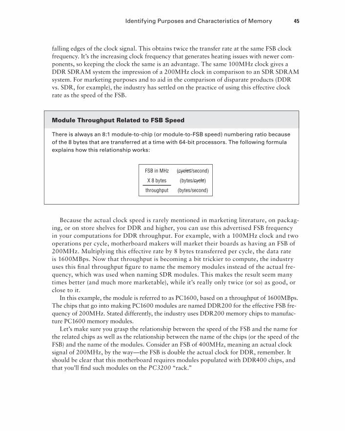
Identifying Purposes and Characteristics of Memory 45
falling edges of the clock signal. This obtains twice the transfer rate at the same FSB clock frequency. It’s the increasing clock frequency that generates heating issues with newer com-ponents, so keeping the clock the same is an advantage. The same 100MHz clock gives a DDR SDRAM system the impression of a 200MHz clock in comparison to an SDR SDRAM system. For marketing purposes and to aid in the comparison of disparate products (DDR vs. SDR, for example), the industry has settled on the practice of using this effective clock rate as the speed of the FSB.
Module Throughput Related to FSB Speed
There is always an 8:1 module-to-chip (or module-to-FSB speed) numbering ratio because of the 8 bytes that are transferred at a time with 64-bit processors. The following formula explains how this relationship works:
FSB in MHz (cycles/second)
X 8 bytes (bytes/cycle)
throughput (bytes/second)
Because the actual clock speed is rarely mentioned in marketing literature, on packag-ing, or on store shelves for DDR and higher, you can use this advertised FSB frequency in your computations for DDR throughput. For example, with a 100MHz clock and two operations per cycle, motherboard makers will market their boards as having an FSB of 200MHz. Multiplying this effective rate by 8 bytes transferred per cycle, the data rate is 1600MBps. Now that throughput is becoming a bit trickier to compute, the industry uses this final throughput figure to name the memory modules instead of the actual fre-quency, which was used when naming SDR modules. This makes the result seem many times better (and much more marketable), while it’s really only twice (or so) as good, or close to it.
In this example, the module is referred to as PC1600, based on a throughput of 1600MBps. The chips that go into making PC1600 modules are named DDR200 for the effective FSB fre-quency of 200MHz. Stated differently, the industry uses DDR200 memory chips to manufac-ture PC1600 memory modules.
Let’s make sure you grasp the relationship between the speed of the FSB and the name for the related chips as well as the relationship between the name of the chips (or the speed of the FSB) and the name of the modules. Consider an FSB of 400MHz, meaning an actual clock signal of 200MHz, by the way—the FSB is double the actual clock for DDR, remember. It should be clear that this motherboard requires modules populated with DDR400 chips, and that you’ll find such modules on the PC3200 “rack.”
86498book.indb 45 7/22/09 5:37:42 AM
46 Chapter 1 Personal Computer System Components
Let’s try another. What do you need for a motherboard that features a 333MHz FSB (actual clock is 166MHz)? Well, just using the 8:1 rule mentioned earlier, you might be on the lookout for a PC2667 module. However, note that sometimes the numbers have to be played with a bit to come up with the industry’s marketing terms. You’ll have an easier time finding PC2700 modules that are designed specifically for a motherboard like yours, with an FSB of 333MHz. The label isn’t always technically accurate, but round numbers sell bet-ter, perhaps. The important concept here is that if you find PC2700 modules and PC2667 modules, there’s absolutely no difference; they both have a 2667MBps throughput rate. Go for the best deal; just make sure the memory manufacturer is reputable.
DDR2 SDRAM
Think of the 2 in DDR2 as yet another multiplier of 2 in the SDRAM technology, using a lower peak voltage to keep power consumption down (1.8V vs. the 2.5V of DDR). Still double-pumping, DDR2, like DDR, uses both sweeps of the clock signal for data transfer. Internally, DDR2 further splits each clock pulse in two, doubling the number of operations it can perform per FSB clock cycle. Through enhancements in the electrical interface and buffers, as well as through adding off-chip drivers, DDR2 nominally produces four times the throughput that SDR is capable of producing.
Continuing the DDR example, DDR2, using a 100MHz actual clock, transfers data in four operations per cycle (effective 400MHz FSB) and still 8 bytes per operation, for a total of 3200MBps. Just like DDR, DDR2 names its chips based on the perceived frequency. In this case, you would be using DDR2-400 chips. DDR2 carries on the effective-FSB frequency method for naming modules but cannot simply call them PC3200 modules because those already exist in the DDR world. DDR2 calls these modules PC2-3200 (note the dash to keep the numeric components separate).
As another example, it should make sense that PC2-5300 modules are populated with DDR2-667 chips. Recall that you might have to play with the numbers a bit. If you multiply the well-known FSB speed of 667MHz by 8 to figure out what modules you need, you might go searching for PC2-5333 modules. You might find someone advertising such modules, but most compatible modules will be labeled PC2-5300 for the same marketability mentioned earlier. They both support 5333MBps of throughput.
DDR3 SDRAM
The next generation of memory devices was designed to roughly double the performance of DDR2 products. Based on the functionality and characteristics of DDR2’s proposed successor, most informed consumers and some members of the industry surely assumed the forthcoming name would be DDR4. This was not to be, however, and DDR3 was born. This naming convention proved that the 2 in DDR2 was not meant to be a multi-plier, but instead a revision mark of sorts. Well, if DDR2 was the second version of DDR, then DDR3 is the third. DDR3 is a memory type that was designed to be twice as fast as the DDR2 memory that operates with the same FSB speed. Just as DDR2 was required to lower power consumption to make up for higher frequencies, DDR3 must do the same. In fact, the peak voltage for DDR3 is only 1.5V.
86498book.indb 46 7/22/09 5:37:42 AM
Identifying Purposes and Characteristics of Memory 47
The most commonly found range of actual clock speeds for DDR3 tends to be from 133MHz at the low end to 250MHz. Because double-pumping continues with DDR3 and because four operations occur at each wave crest (8 operations per cycle), this frequency range translates to common FSB implementations from 1066MHz to 2000MHz in DDR3 systems. Naming these memory devices follows the conventions established earlier. There-fore, if you buy a motherboard with a 1600MHz FSB, you know immediately that you need a memory module populated with DDR3-1600 chips because the chips are always named for the FSB speed. Using the 8:1 module-to-chip/FSB naming rule, the modules you need would be called PC3-12800, supporting a 12800MBps throughput.
The earliest DDR3 chips, however, were based on a 100MHz actual clock signal, so we can build on our earlier example, which was also based on an actual clock rate of 100MHz. With 8 operations per cycle, the FSB on DDR3 motherboards is rated at 800MHz, quite a lot of efficiency while still not needing to change the original clock our examples began with. Applying the 8:1 rule again, the resulting RAM modules for this motherboard are called PC3-6400 and support a throughput of 6400MBps, carrying chips called DDR3-800, again named for the FSB speed.
Choosing the Right Memory for Your CPU
Let’s say you head down to your local computer store, where motherboards, CPUs, memory, and other computer components are sold a la carte. You’re interested in putting together your own system from scratch. Usually, you will have a CPU in mind that you would like to use in your new system. Assuming you choose, for example, an Intel Core 2 Quad Q8200 processor, you discover you need a motherboard that has an LGA 775 socket and supports a frontside bus of 1333MHz. You could assume you need DDR3 memory because DDR2 tops out around 1066MHz (PC2-8500). If you’d rather not assume, you can consult the chosen motherboard’s documentation or display slick and confirm your suspicions. If you’re right, you’ll be buying at least one stick of your favorite capacity of PC3-10666 (multiplying 1333 by 8), two sticks if you need to feed a hungry dual-channel motherboard. In case you missed it, PC3-10666 modules are made using DDR3-1333 chips, so named for the speed of the FSB. Recall the 8:1 module-to-chip/FSB naming convention.
DRDRAM
Direct Rambus DRAM (DRDRAM), named for Rambus, the company that designed it, is a proprietary SDRAM technology, sometimes called RDRAM, dropping “direct.” DRDRAM can be found in fewer new systems today than just a few years ago. This is because Intel once had a contractual agreement with Rambus to create chipsets for the motherboards of Intel and others that would primarily use DRDRAM in exchange for
86498book.indb 47 7/22/09 5:37:43 AM
48 Chapter 1 Personal Computer System Components
special licensing considerations and royalties from Rambus. The contract ran from 1996 until 2002. In 1999, Intel launched the first motherboards with DRDRAM support. Until then, Rambus could be found mainly in gaming consoles and home theater components. DRDRAM did not impact the market as Intel had hoped, and so motherboard manufactur-ers got around Intel’s obligation by using chipsets from VIA Technologies, leading to the rise of that company.
Although other specifications preceded it, the first motherboard DRDRAM model was known as PC800. As with non-DRDRAM specifications that use this nam-ing convention, PC800 specifies that, using a faster 400MHz actual clock signal and double-pumping like DDR SDRAM, an effective frequency and FSB speed of 800MHz is created. DRDRAM was originally named in a dissimilar fashion to other forms of SDRAM, instead based on the FSB speed. You might recall, for those memory types, that the FSB speed was used to name the actual chips on the modules, not the modules themselves. PC800 DRDRAM, then, features a double-pumped 800MHz FSB. Newer modules, such as the 32-bit RIMM 6400, are named for their actual throughput, 6400MBps, in this case. The section “RIMM” in this chapter details the physical details of the modules.
There are only 16 data pins per channel with DRDRAM, versus 64 bits per channel in other SDRAM implementations. This fact results in a 16-bit (2-byte) channel. A 2-byte packet, therefore, is exchanged during each read/write cycle, bringing the overall transfer rate of PC800 DRDRAM to 1600MBps per channel. DRDRAM chipsets require two 16-bit channels to communicate simultaneously for the same read/write request, creating a mandatory 32-bit dual-channel mode. Two PC800 DRDRAM modules in a dual-channel configuration produce transfer rates of 3200MBps. In motherboards that support 32-bit modules, you would use a single RIMM 3200 to achieve this 3200MBps of throughput, using the same actual 400MHz clock and 800MHz FSB and transferring 4 bytes at a time.
Despite DRDRAM’s performance advantages, it has some drawbacks that keep it from taking over the market. Increased latency, heat output, complexity in the manufacturing pro-cess, and cost are the primary shortcomings. The additional heat that individual DRDRAM chips put out led to the requirement for heat sinks on all modules. High manufacturing costs and high licensing fees led to triple the cost to consumers over SDR, although today there is more parity between the prices.
In 2003, free from its contractual obligations to Rambus, Intel released the i875P chipset. This new chipset provides support for a dual-channel platform using standard PC3200 DDR modules. Dual-channel DDR transfers 16 bytes (128 bits) per read/write request, giving PC3200 a total throughput rate of 6400MBps. As a result, and because of the advent of DDR2 and DDR3, DRDRAM no longer holds any performance advantage.
To put each of the SDRAM types into perspective, consult Table 1.2, which sum-marizes how each technology in the SDRAM arena would achieve a transfer rate of 3200MBps, even if only theoretically. For example, PC400 doesn’t exist in the SDR SDRAM world.
86498book.indb 48 7/22/09 5:37:43 AM
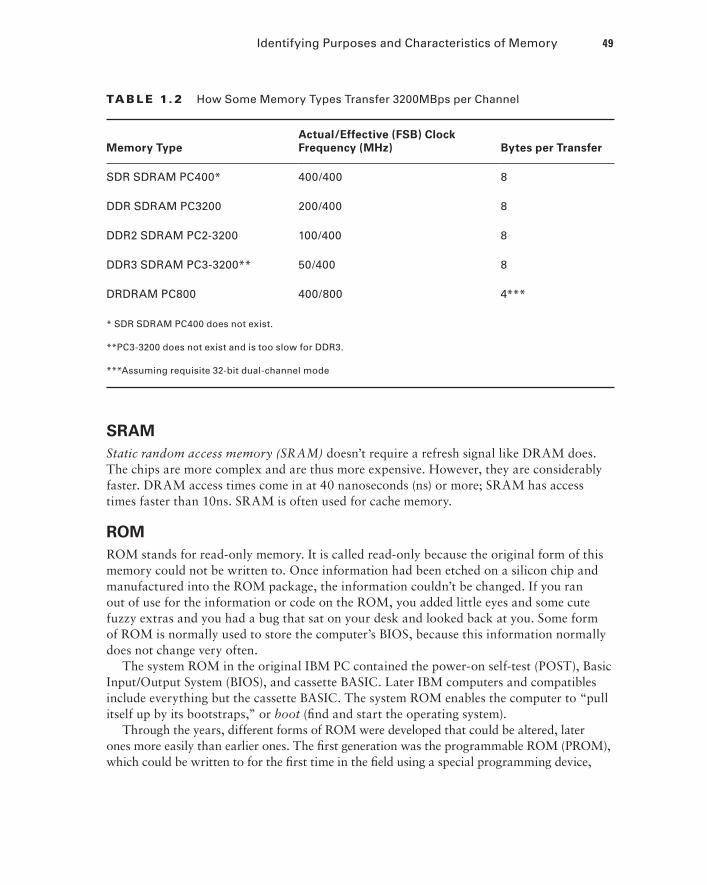
Identifying Purposes and Characteristics of Memory 49
TA B LE 1. 2 How Some Memory Types Transfer 3200MBps per Channel
Memory Type
Actual/Effective (FSB) Clock
Frequency (MHz) Bytes per Transfer
SDR SDRAM PC400* 400/400 8
DDR SDRAM PC3200 200/400 8
DDR2 SDRAM PC2-3200 100/400 8
DDR3 SDRAM PC3-3200** 50/400 8
DRDRAM PC800 400/800 4***
* SDR SDRAM PC400 does not exist.
**PC3-3200 does not exist and is too slow for DDR3.
***Assuming requisite 32-bit dual-channel mode
SRAM
Static random access memory (SRAM) doesn’t require a refresh signal like DRAM does. The chips are more complex and are thus more expensive. However, they are considerably faster. DRAM access times come in at 40 nanoseconds (ns) or more; SRAM has access times faster than 10ns. SRAM is often used for cache memory.
ROM
ROM stands for read-only memory. It is called read-only because the original form of this memory could not be written to. Once information had been etched on a silicon chip and manufactured into the ROM package, the information couldn’t be changed. If you ran out of use for the information or code on the ROM, you added little eyes and some cute fuzzy extras and you had a bug that sat on your desk and looked back at you. Some form of ROM is normally used to store the computer’s BIOS, because this information normally does not change very often.
The system ROM in the original IBM PC contained the power-on self-test (POST), Basic Input/Output System (BIOS), and cassette BASIC. Later IBM computers and compatibles include everything but the cassette BASIC. The system ROM enables the computer to “pull itself up by its bootstraps,” or boot (find and start the operating system).
Through the years, different forms of ROM were developed that could be altered, later ones more easily than earlier ones. The first generation was the programmable ROM (PROM), which could be written to for the first time in the field using a special programming device,
86498book.indb 49 7/22/09 5:37:43 AM
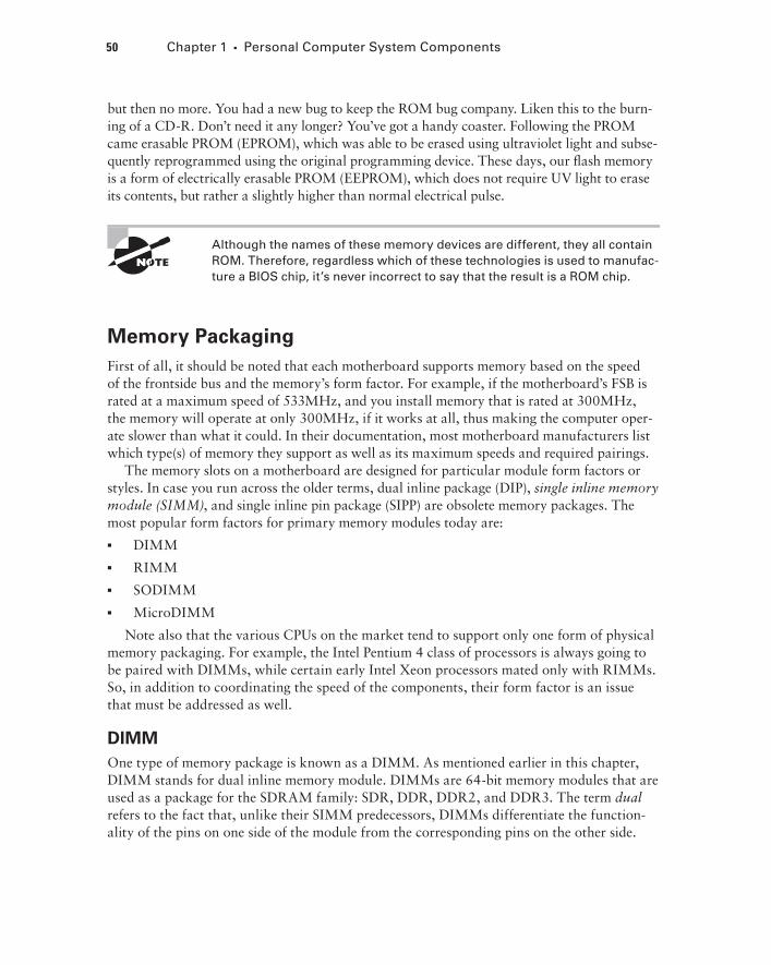
50 Chapter 1 Personal Computer System Components
but then no more. You had a new bug to keep the ROM bug company. Liken this to the burn-ing of a CD-R. Don’t need it any longer? You’ve got a handy coaster. Following the PROM came erasable PROM (EPROM), which was able to be erased using ultraviolet light and subse-quently reprogrammed using the original programming device. These days, our flash memory is a form of electrically erasable PROM (EEPROM), which does not require UV light to erase its contents, but rather a slightly higher than normal electrical pulse.
Although the names of these memory devices are different, they all contain ROM. Therefore, regardless which of these technologies is used to manufac-ture a BIOS chip, it’s never incorrect to say that the result is a ROM chip.
Memory Packaging
First of all, it should be noted that each motherboard supports memory based on the speed of the frontside bus and the memory’s form factor. For example, if the motherboard’s FSB is rated at a maximum speed of 533MHz, and you install memory that is rated at 300MHz, the memory will operate at only 300MHz, if it works at all, thus making the computer oper-ate slower than what it could. In their documentation, most motherboard manufacturers list which type(s) of memory they support as well as its maximum speeds and required pairings.
The memory slots on a motherboard are designed for particular module form factors or styles. In case you run across the older terms, dual inline package (DIP), single inline memory module (SIMM), and single inline pin package (SIPP) are obsolete memory packages. The most popular form factors for primary memory modules today are:
DIMM
RIMM
SODIMM
MicroDIMM
Note also that the various CPUs on the market tend to support only one form of physical memory packaging. For example, the Intel Pentium 4 class of processors is always going to be paired with DIMMs, while certain early Intel Xeon processors mated only with RIMMs. So, in addition to coordinating the speed of the components, their form factor is an issue that must be addressed as well.
DIMM
One type of memory package is known as a DIMM. As mentioned earlier in this chapter, DIMM stands for dual inline memory module. DIMMs are 64-bit memory modules that are used as a package for the SDRAM family: SDR, DDR, DDR2, and DDR3. The term dual refers to the fact that, unlike their SIMM predecessors, DIMMs differentiate the function-ality of the pins on one side of the module from the corresponding pins on the other side.
86498book.indb 50 7/22/09 5:37:43 AM
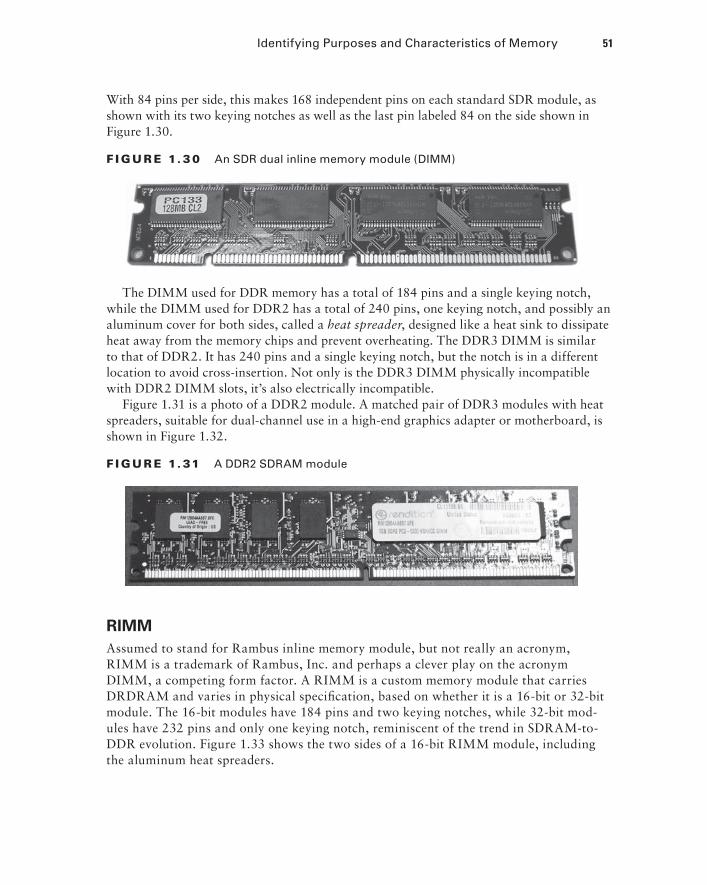
Identifying Purposes and Characteristics of Memory 51
With 84 pins per side, this makes 168 independent pins on each standard SDR module, as shown with its two keying notches as well as the last pin labeled 84 on the side shown in Figure 1.30.
F I GU R E 1. 3 0 An SDR dual inline memory module (DIMM)
The DIMM used for DDR memory has a total of 184 pins and a single keying notch, while the DIMM used for DDR2 has a total of 240 pins, one keying notch, and possibly an aluminum cover for both sides, called a heat spreader, designed like a heat sink to dissipate heat away from the memory chips and prevent overheating. The DDR3 DIMM is similar to that of DDR2. It has 240 pins and a single keying notch, but the notch is in a different location to avoid cross-insertion. Not only is the DDR3 DIMM physically incompatible with DDR2 DIMM slots, it’s also electrically incompatible.
Figure 1.31 is a photo of a DDR2 module. A matched pair of DDR3 modules with heat spreaders, suitable for dual-channel use in a high-end graphics adapter or motherboard, is shown in Figure 1.32.
F I GU R E 1. 31 A DDR2 SDRAM module
RIMM
Assumed to stand for Rambus inline memory module, but not really an acronym, RIMM is a trademark of Rambus, Inc. and perhaps a clever play on the acronym DIMM, a competing form factor. A RIMM is a custom memory module that carries DRDRAM and varies in physical specification, based on whether it is a 16-bit or 32-bit module. The 16-bit modules have 184 pins and two keying notches, while 32-bit mod-ules have 232 pins and only one keying notch, reminiscent of the trend in SDRAM-to-DDR evolution. Figure 1.33 shows the two sides of a 16-bit RIMM module, including the aluminum heat spreaders.
86498book.indb 51 7/22/09 5:37:44 AM
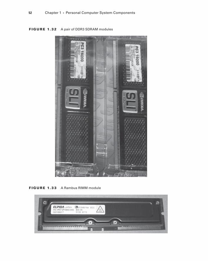
52 Chapter 1 Personal Computer System Components
F I GU R E 1. 32 A pair of DDR3 SDRAM modules
F I GU R E 1. 3 3 A Rambus RIMM module
86498book.indb 52 7/22/09 5:37:46 AM
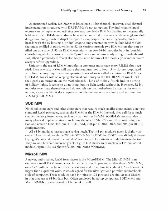
Identifying Purposes and Characteristics of Memory 53
As mentioned earlier, DRDRAM is based on a 16-bit channel. However, dual-channel implementation is required with DRDRAM; it’s not an option. The dual-channel archi-tecture can be implemented utilizing two separate 16-bit RIMMs (leading to the generally held view that RIMMs must always be installed in pairs) or the newer 32-bit single-module design (not doing much to dispel the “pair” view, despite the facts). Typically, mother-boards with the 16-bit single- or dual-channel implementation provide four RIMM slots that must be filled in pairs, while the 32-bit versions provide two RIMM slots that can be filled one at a time. A 32-bit RIMM essentially has two 16-bit modules built in (possibly contributing to the persistence of the “pair” view) and requires only a single motherboard slot, albeit a physically different slot. So you must be sure of the module your motherboard accepts before upgrading.
Unique to the use of RIMM modules, a computer must have every RIMM slot occu-pied. Even one vacant slot will cause the computer not to boot. Any slot not populated with live memory requires an inexpensive blank of sorts called a continuity RIMM, or C-RIMM, for its role of keeping electrical continuity in the DRDRAM channel until the signal can terminate on the motherboard. Think of it like a fusible link in a string of holiday lights. It seems to do nothing, but no light works without it. However, 32-bit modules terminate themselves and do not rely on the motherboard circuitry for termi-nation, so vacant 32-bit slots require a module known as a continuity and termination RIMM (CT-RIMM).
SODIMM
Notebook computers and other computers that require much smaller components don’t use standard RAM packages, such as the SIMM or the DIMM. Instead, they call for a much smaller memory form factor, such as a small outline DIMM. SODIMMs are available in many physical implementations, including the older 32-bit (72- and 100-pin) configura-tion and newer 64-bit (144-pin SDR SDRAM, 200-pin DDR/DDR2, and 204-pin DDR3) configurations.
All 64-bit modules have a single keying notch. The 144-pin module’s notch is slightly off-center. Note that although the 200-pin SODIMMs for DDR and DDR2 have slightly different keying, it’s not so different that you don’t need to pay close attention to differentiate the two. They are not, however, interchangeable. Figure 1.34 shows an example of a 144-pin, 64-bit module. Figure 1.35 is a photo of a 200-pin DDR2 SODIMM.
MicroDIMM
A newer, and smaller, RAM form factor is the MicroDIMM. The MicroDIMM is an extremely small RAM form factor. In fact, it is over 50 percent smaller than a SODIMM, only 45.5 millimeters (about 1.75 inches) long and 30 millimeters (about 1.2 inches—a bit bigger than a quarter) wide. It was designed for the ultralight and portable subnotebook style of computer. These modules have 144 pins or 172 pins and are similar to a DIMM in that they use a 64-bit data bus. Often employed in laptop computers, SODIMMs and MicroDIMMs are mentioned in Chapter 4 as well.
86498book.indb 53 7/22/09 5:37:46 AM
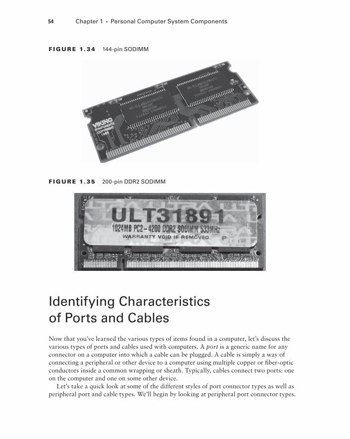
54 Chapter 1 Personal Computer System Components
F I GU R E 1. 3 4 144-pin SODIMM
F I G U R E 1. 3 5 200-pin DDR2 SODIMM
Identifying Characteristics of Ports and CablesNow that you’ve learned the various types of items found in a computer, let’s discuss the various types of ports and cables used with computers. A port is a generic name for any connector on a computer into which a cable can be plugged. A cable is simply a way of connecting a peripheral or other device to a computer using multiple copper or fiber-optic conductors inside a common wrapping or sheath. Typically, cables connect two ports: one on the computer and one on some other device.
Let’s take a quick look at some of the different styles of port connector types as well as peripheral port and cable types. We’ll begin by looking at peripheral port connector types.
86498book.indb 54 7/22/09 5:37:46 AM
Identifying Characteristics of Ports and Cables 55
Peripheral Port Connector Types
Computer ports are interfaces that allow other devices to be connected to a computer. Their appearance varies widely, depending on their function. In this section we’ll examine the fol-lowing types of peripheral ports:
D-subminiature
RJ-series
Other types
D-subminiature Connectors
D-sub connectors, for a number of years the most common style of connector found on computers, are typically designated with DXn, where the letter X is replaced by the let-ters A through E, which refer to the size of the connector, and the letter n is replaced by the number of pins or sockets in the connector. D-sub connectors are usually shaped like a trapezoid, as you can see in Figure 1.36. The nice part about these connectors is that only one orientation is possible. If you try to connect them upside down or try to connect a male connector to another male connector, they just won’t go together, and the connection can’t be made. Table 1.3 lists common D-sub ports and connectors as well as their most common uses. Be on the lookout for the casual use of “DB” to represent any D-sub connector. This is very common and is accepted as an unwritten de facto standard.
At the bottom left in Figure 1.36 is a DE15F 15-pin video port, in the center is a DB25F 25-pin female printer port, and on the right is a DE9M 9-pin male serial port.
TA B LE 1. 3 Common D-sub Connectors
Connector Gender Use
DE9 Male Serial port
DE9 Female Connector on a serial cable
DB25 Male Serial port or connector on a parallel cable
DB25 Female Parallel port, or connector on a serial cable
DA15 Female Game port or MIDI port
DA15 Male Connector on a game peripheral cable or MIDI cable
DE15 Female Video port (has three rows of 5 pins as opposed to two rows)
DE15 Male Connector on a monitor cable
86498book.indb 55 7/22/09 5:37:46 AM
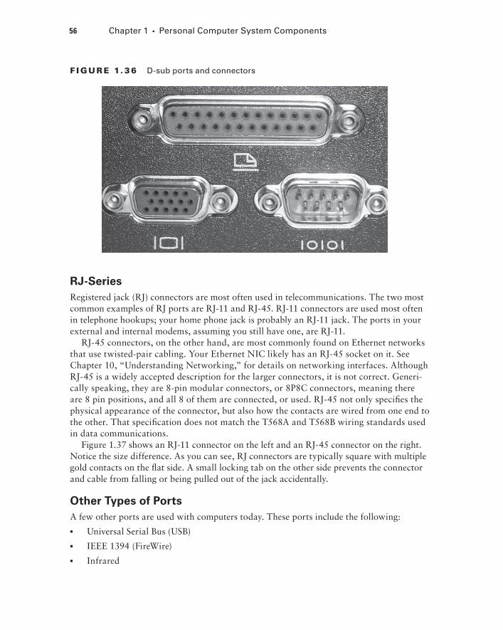
56 Chapter 1 Personal Computer System Components
F I GU R E 1. 36 D-sub ports and connectors
RJ-Series
Registered jack (RJ) connectors are most often used in telecommunications. The two most common examples of RJ ports are RJ-11 and RJ-45. RJ-11 connectors are used most often in telephone hookups; your home phone jack is probably an RJ-11 jack. The ports in your external and internal modems, assuming you still have one, are RJ-11.
RJ-45 connectors, on the other hand, are most commonly found on Ethernet networks that use twisted-pair cabling. Your Ethernet NIC likely has an RJ-45 socket on it. See Chapter 10, “Understanding Networking,” for details on networking interfaces. Although RJ-45 is a widely accepted description for the larger connectors, it is not correct. Generi-cally speaking, they are 8-pin modular connectors, or 8P8C connectors, meaning there are 8 pin positions, and all 8 of them are connected, or used. RJ-45 not only specifies the physical appearance of the connector, but also how the contacts are wired from one end to the other. That specification does not match the T568A and T568B wiring standards used in data communications.
Figure 1.37 shows an RJ-11 connector on the left and an RJ-45 connector on the right. Notice the size difference. As you can see, RJ connectors are typically square with multiple gold contacts on the flat side. A small locking tab on the other side prevents the connector and cable from falling or being pulled out of the jack accidentally.
Other Types of Ports
A few other ports are used with computers today. These ports include the following:
Universal Serial Bus (USB)
IEEE 1394 (FireWire)
Infrared
86498book.indb 56 7/22/09 5:37:47 AM
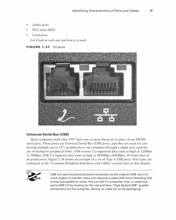
Identifying Characteristics of Ports and Cables 57
Audio jacks
PS/2 (mini-DIN)
Centronics
Let’s look at each one and how it is used.
F I GU R E 1. 37 RJ ports
Universal Serial Bus (USB)
Most computers built after 1997 have one or more flat ports in place of one DE9M serial port. These ports are Universal Serial Bus (USB) ports, and they are used for con-necting multiple (up to 127) peripherals to one computer through a single port (and the use of multiport peripheral hubs). USB version 1.1 supported data rates as high as 12Mbps (1.5MBps). USB 2.0 supports data rates as high as 480Mbps (60MBps), 40 times that of its predecessor. Figure 1.38 shows an example of a set of Type A USB ports. Port types are explained in the “Common Peripheral Interfaces and Cables” section later in this chapter.
USB 2.0 uses the same physical connection as the original USB, but it is much higher in transfer rates and requires a cable with more shielding that is less susceptible to noise. You can tell if a computer, hub, or cable sup-ports USB 2.0 by looking for the red and blue “High Speed USB” graphic somewhere on the computer, device, or cable (or on its packaging).
86498book.indb 57 7/22/09 5:37:48 AM
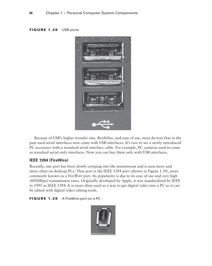
58 Chapter 1 Personal Computer System Components
F I GU R E 1. 3 8 USB ports
Because of USB’s higher transfer rate, flexibility, and ease of use, most devices that in the past used serial interfaces now come with USB interfaces. It’s rare to see a newly introduced PC accessory with a standard serial interface cable. For example, PC cameras used to come as standard serial-only interfaces. Now you can buy them only with USB interfaces.
IEEE 1394 (FireWire)
Recently, one port has been slowly creeping into the mainstream and is seen more and more often on desktop PCs. That port is the IEEE 1394 port (shown in Figure 1.39), more commonly known as a FireWire port. Its popularity is due to its ease of use and very high (400Mbps) transmission rates. Originally developed by Apple, it was standardized by IEEE in 1995 as IEEE 1394. It is most often used as a way to get digital video into a PC so it can be edited with digital video editing tools.
F I GU R E 1. 3 9 A FireWire port on a PC
86498book.indb 58 7/22/09 5:37:48 AM
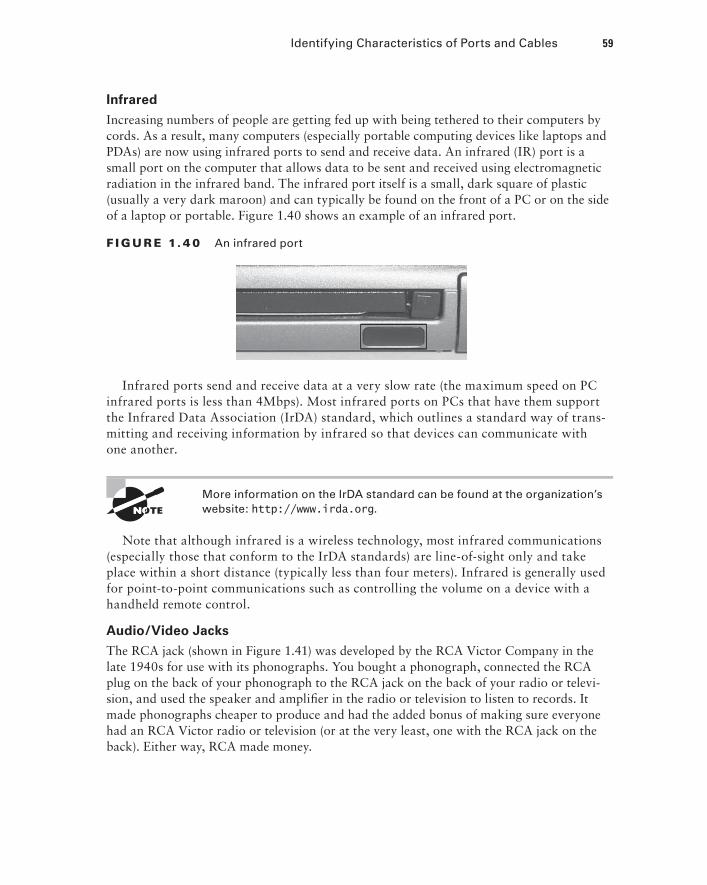
Identifying Characteristics of Ports and Cables 59
Infrared
Increasing numbers of people are getting fed up with being tethered to their computers by cords. As a result, many computers (especially portable computing devices like laptops and PDAs) are now using infrared ports to send and receive data. An infrared (IR) port is a small port on the computer that allows data to be sent and received using electromagnetic radiation in the infrared band. The infrared port itself is a small, dark square of plastic (usually a very dark maroon) and can typically be found on the front of a PC or on the side of a laptop or portable. Figure 1.40 shows an example of an infrared port.
F I GU R E 1. 4 0 An infrared port
Infrared ports send and receive data at a very slow rate (the maximum speed on PC infrared ports is less than 4Mbps). Most infrared ports on PCs that have them support the Infrared Data Association (IrDA) standard, which outlines a standard way of trans-mitting and receiving information by infrared so that devices can communicate with one another.
More information on the IrDA standard can be found at the organization’s website: .
Note that although infrared is a wireless technology, most infrared communications (especially those that conform to the IrDA standards) are line-of-sight only and take place within a short distance (typically less than four meters). Infrared is generally used for point-to-point communications such as controlling the volume on a device with a handheld remote control.
Audio/Video Jacks
The RCA jack (shown in Figure 1.41) was developed by the RCA Victor Company in the late 1940s for use with its phonographs. You bought a phonograph, connected the RCA plug on the back of your phonograph to the RCA jack on the back of your radio or televi-sion, and used the speaker and amplifier in the radio or television to listen to records. It made phonographs cheaper to produce and had the added bonus of making sure everyone had an RCA Victor radio or television (or at the very least, one with the RCA jack on the back). Either way, RCA made money.
86498book.indb 59 7/22/09 5:37:48 AM
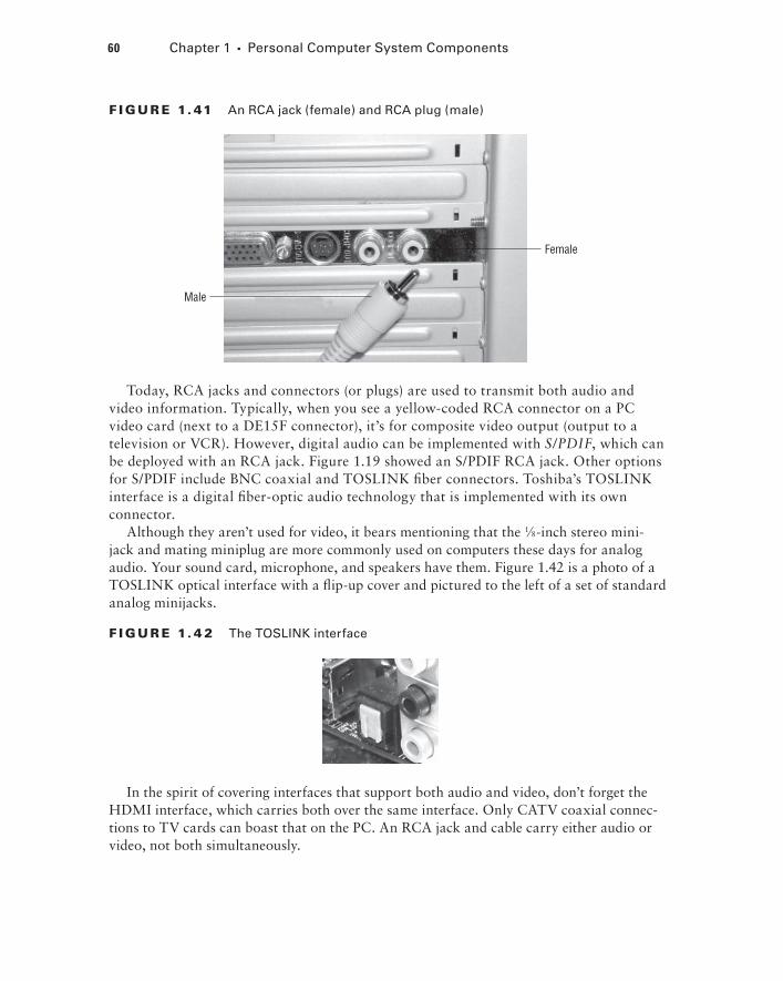
60 Chapter 1 Personal Computer System Components
F I GU R E 1. 41 An RCA jack (female) and RCA plug (male)
Female
Male
Today, RCA jacks and connectors (or plugs) are used to transmit both audio and video information. Typically, when you see a yellow-coded RCA connector on a PC video card (next to a DE15F connector), it’s for composite video output (output to a television or VCR). However, digital audio can be implemented with S/PDIF, which can be deployed with an RCA jack. Figure 1.19 showed an S/PDIF RCA jack. Other options for S/PDIF include BNC coaxial and TOSLINK fiber connectors. Toshiba’s TOSLINK interface is a digital fiber-optic audio technology that is implemented with its own connector.
Although they aren’t used for video, it bears mentioning that the 1⁄8-inch stereo mini-jack and mating miniplug are more commonly used on computers these days for analog audio. Your sound card, microphone, and speakers have them. Figure 1.42 is a photo of a TOSLINK optical interface with a flip-up cover and pictured to the left of a set of standard analog minijacks.
F I GU R E 1. 4 2 The TOSLINK interface
In the spirit of covering interfaces that support both audio and video, don’t forget the HDMI interface, which carries both over the same interface. Only CATV coaxial connec-tions to TV cards can boast that on the PC. An RCA jack and cable carry either audio or video, not both simultaneously.
86498book.indb 60 7/22/09 5:37:50 AM
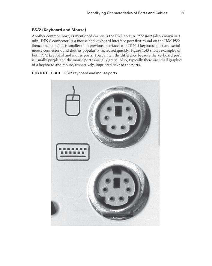
Identifying Characteristics of Ports and Cables 61
PS/2 (Keyboard and Mouse)
Another common port, as mentioned earlier, is the PS/2 port. A PS/2 port (also known as a mini-DIN 6 connector) is a mouse and keyboard interface port first found on the IBM PS/2 (hence the name). It is smaller than previous interfaces (the DIN-5 keyboard port and serial mouse connector), and thus its popularity increased quickly. Figure 1.43 shows examples of both PS/2 keyboard and mouse ports. You can tell the difference because the keyboard port is usually purple and the mouse port is usually green. Also, typically there are small graphics of a keyboard and mouse, respectively, imprinted next to the ports.
F I GU R E 1. 4 3 PS/2 keyboard and mouse ports
86498book.indb 61 7/22/09 5:37:50 AM
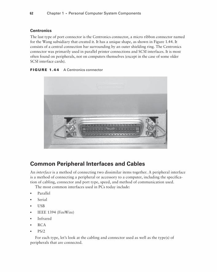
62 Chapter 1 Personal Computer System Components
Centronics
The last type of port connector is the Centronics connector, a micro ribbon connector named for the Wang subsidiary that created it. It has a unique shape, as shown in Figure 1.44. It consists of a central connection bar surrounding by an outer shielding ring. The Centronics connector was primarily used in parallel printer connections and SCSI interfaces. It is most often found on peripherals, not on computers themselves (except in the case of some older SCSI interface cards).
F I GU R E 1. 4 4 A Centronics connector
Common Peripheral Interfaces and Cables
An interface is a method of connecting two dissimilar items together. A peripheral interface is a method of connecting a peripheral or accessory to a computer, including the specifica-tion of cabling, connector and port type, speed, and method of communication used.
The most common interfaces used in PCs today include:
Parallel
Serial
USB
IEEE 1394 (FireWire)
Infrared
RCA
PS/2
For each type, let’s look at the cabling and connector used as well as the type(s) of peripherals that are connected.
86498book.indb 62 7/22/09 5:37:51 AM
Identifying Characteristics of Ports and Cables 63
Parallel
For many years, the most popular type of interface available on computers was the parallel interface. Parallel communications take the interstate approach to data communications. Normally, interstate travel is faster than driving on city roads. This is the case mainly because you can fit multiple cars going the same direction on the same highway by using multiple lanes. On the return trip, you take a similar path, but on a completely separate road. The parallel interface (an example is shown at the top of Figure 1.36) transfers data 8 bits at a time over eight separate transmit wires inside a parallel cable (one bit per wire). Normal parallel interfaces use a DB-25 female connector on the computer to transfer data to peripherals. Parallel was faster than the original serial technology, which was also once used for printers in electrically noisy environments or at greater distances from the com-puter, but the advent of USB has brought serial, fast serial, back to the limelight.
The most common use of the parallel interface is printer communication. There are three major types: standard, bidirectional, and enhanced parallel ports. Let’s look at the differences between the three.
Standard Parallel Ports
The standard parallel port only transmits data out of the computer. It cannot receive data (except for a single wire carrying a Ready signal). This parallel port came with the original IBM PC, XT, and AT. It can transmit data at 150KBps and is commonly used to transmit data to printers. This technology also had a maximum transmission distance of 10 feet.
Bidirectional Parallel Ports
As its name suggests, the bidirectional parallel port has one important advantage over a standard parallel port: it can both transmit and receive data. These parallel ports are capable of interfacing with such devices as external CD-ROM drives and external paral-lel port backup drives (Zip, Jaz, and tape drives). Most computers made since 1994 have a bidirectional parallel port.
In order for bidirectional communication to occur properly, the cable must support bidirectional communication as well.
Enhanced Parallel Ports
As more people began using parallel ports to interface with devices other than printers, they started to notice that the available speed wasn’t good enough. Double-speed CD-ROM drives had a transfer rate of 300KBps, but the parallel port could transfer data at only 150KBps, thus limiting the speed at which a computer could retrieve data from an external device. To solve that problem, the Institute of Electrical and Electronics Engineers (IEEE) came up with a standard for enhanced parallel ports called IEEE 1284. The IEEE 1284 standard provides for greater data transfer speeds and the ability to send memory addresses as well as data through a parallel port. This standard allows the parallel port to theoreti-cally act as an extension to the main bus. In addition, these ports are backward compatible
86498book.indb 63 7/22/09 5:37:51 AM
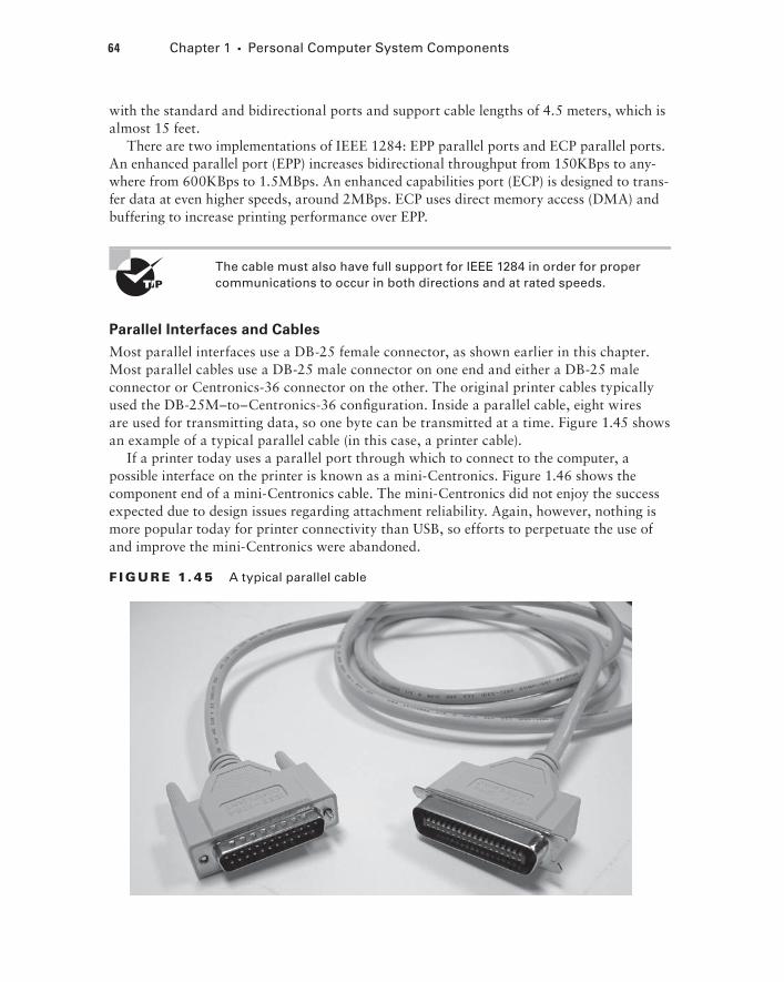
64 Chapter 1 Personal Computer System Components
with the standard and bidirectional ports and support cable lengths of 4.5 meters, which is almost 15 feet.
There are two implementations of IEEE 1284: EPP parallel ports and ECP parallel ports. An enhanced parallel port (EPP) increases bidirectional throughput from 150KBps to any-where from 600KBps to 1.5MBps. An enhanced capabilities port (ECP) is designed to trans-fer data at even higher speeds, around 2MBps. ECP uses direct memory access (DMA) and buffering to increase printing performance over EPP.
The cable must also have full support for IEEE 1284 in order for proper communications to occur in both directions and at rated speeds.
Parallel Interfaces and Cables
Most parallel interfaces use a DB-25 female connector, as shown earlier in this chapter. Most parallel cables use a DB-25 male connector on one end and either a DB-25 male connector or Centronics-36 connector on the other. The original printer cables typically used the DB-25M–to–Centronics-36 configuration. Inside a parallel cable, eight wires are used for transmitting data, so one byte can be transmitted at a time. Figure 1.45 shows an example of a typical parallel cable (in this case, a printer cable).
If a printer today uses a parallel port through which to connect to the computer, a possible interface on the printer is known as a mini-Centronics. Figure 1.46 shows the component end of a mini-Centronics cable. The mini-Centronics did not enjoy the success expected due to design issues regarding attachment reliability. Again, however, nothing is more popular today for printer connectivity than USB, so efforts to perpetuate the use of and improve the mini-Centronics were abandoned.
F I GU R E 1. 4 5 A typical parallel cable
86498book.indb 64 7/22/09 5:37:52 AM
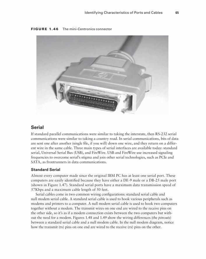
Identifying Characteristics of Ports and Cables 65
F I GU R E 1. 4 6 The mini-Centronics connector
Serial
If standard parallel communications were similar to taking the interstate, then RS-232 serial communications were similar to taking a country road. In serial communications, bits of data are sent one after another (single file, if you will) down one wire, and they return on a differ-ent wire in the same cable. Three main types of serial interfaces are available today: standard serial, Universal Serial Bus (USB), and FireWire. USB and FireWire use increased signaling frequencies to overcome serial’s stigma and join other serial technologies, such as PCIe and SATA, as frontrunners in data communications.
Standard Serial
Almost every computer made since the original IBM PC has at least one serial port. These computers are easily identified because they have either a DE-9 male or a DB-25 male port (shown in Figure 1.47). Standard serial ports have a maximum data transmission speed of 57Kbps and a maximum cable length of 50 feet.
Serial cables come in two common wiring configurations: standard serial cable and null modem serial cable. A standard serial cable is used to hook various peripherals such as modems and printers to a computer. A null modem serial cable is used to hook two computers together without a modem. The transmit wires on one end are wired to the receive pins on the other side, so it’s as if a modem connection exists between the two computers but with-out the need for a modem. Figures 1.48 and 1.49 show the wiring differences (the pinouts) between a standard serial cable and a null modem cable. In the null modem diagram, notice how the transmit (tx) pins on one end are wired to the receive (rx) pins on the other.
86498book.indb 65 7/22/09 5:37:53 AM
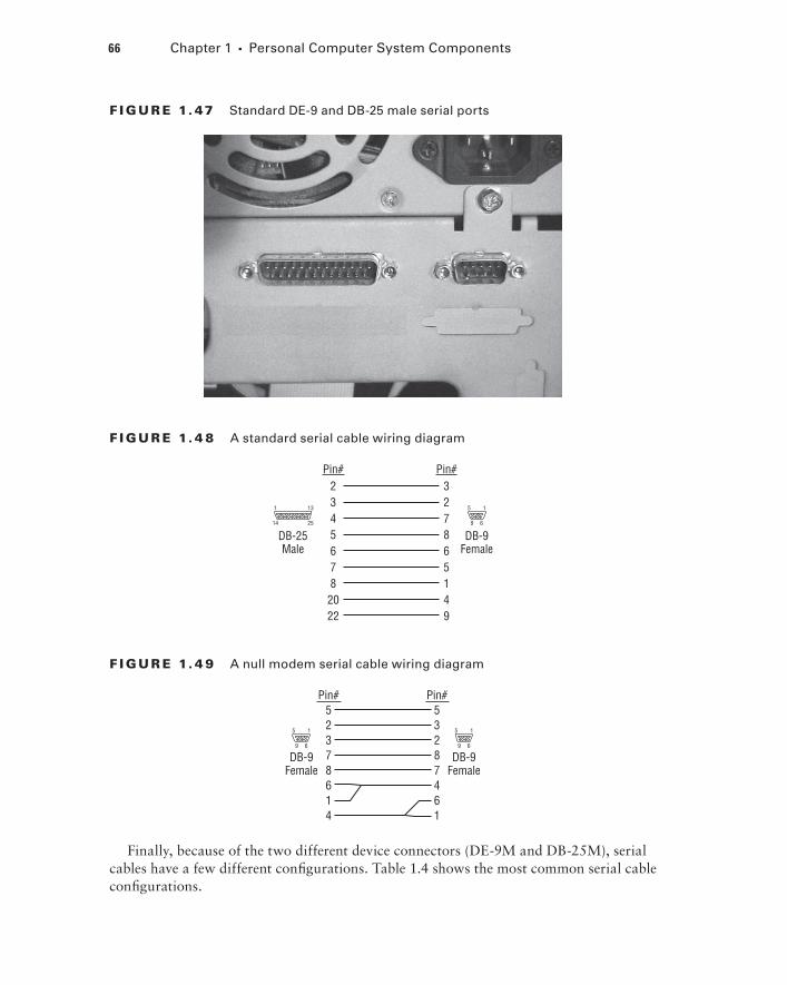
66 Chapter 1 Personal Computer System Components
F I GU R E 1. 47 Standard DE-9 and DB-25 male serial ports
F I GU R E 1. 4 8 A standard serial cable wiring diagram
2345678
2022
327865149
Pin#
5 1
9 6
1 13
14 25
Pin#
DB-25Male
DB-9Female
F I GU R E 1. 4 9 A null modem serial cable wiring diagram
Pin#52378614
53287461
Pin#
DB-9Female
5 1
9 6
DB-9Female
5 1
9 6
Finally, because of the two different device connectors (DE-9M and DB-25M), serial cables have a few different configurations. Table 1.4 shows the most common serial cable configurations.
86498book.indb 66 7/22/09 5:37:54 AM
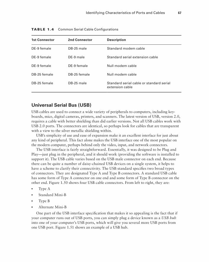
Identifying Characteristics of Ports and Cables 67
TA B LE 1. 4 Common Serial Cable Configurations
1st Connector 2nd Connector Description
DE-9 female DB-25 male Standard modem cable
DE-9 female DE-9 male Standard serial extension cable
DE-9 female DE-9 female Null modem cable
DB-25 female DB-25 female Null modem cable
DB-25 female DB-25 male Standard serial cable or standard serial extension cable
Universal Serial Bus (USB)
USB cables are used to connect a wide variety of peripherals to computers, including key-boards, mice, digital cameras, printers, and scanners. The latest version of USB, version 2.0, requires a cable with better shielding than did earlier versions. Not all USB cables work with USB 2.0 ports. The connectors are identical, so perhaps look for cables that are transparent with a view to the silver metallic shielding within.
USB’s simplicity of use and ease of expansion make it an excellent interface for just about any kind of peripheral. This fact alone makes the USB interface one of the most popular on the modern computer, perhaps behind only the video, input, and network connectors.
The USB interface is fairly straightforward. Essentially, it was designed to be Plug and Play—just plug in the peripheral, and it should work (providing the software is installed to support it). The USB cable varies based on the USB male connector on each end. Because there can be quite a number of daisy-chained USB devices on a single system, it helps to have a scheme to clarify their connectivity. The USB standard specifies two broad types of connectors. They are designated Type A and Type B connectors. A standard USB cable has some form of Type A connector on one end and some form of Type B connector on the other end. Figure 1.50 shows four USB cable connectors. From left to right, they are:
Type A
Standard Mini-B
Type B
Alternate Mini-B
One part of the USB interface specification that makes it so appealing is the fact that if your computer runs out of USB ports, you can simply plug a device known as a USB hub into one of your computer’s USB ports, which will give you several more USB ports from one USB port. Figure 1.51 shows an example of a USB hub.
86498book.indb 67 7/22/09 5:37:54 AM
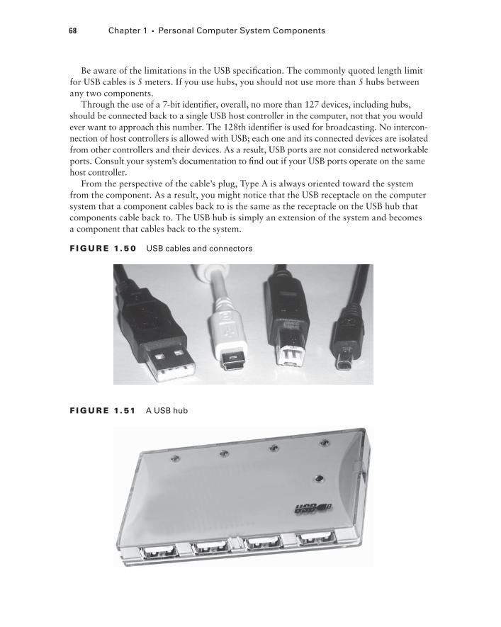
68 Chapter 1 Personal Computer System Components
Be aware of the limitations in the USB specification. The commonly quoted length limit for USB cables is 5 meters. If you use hubs, you should not use more than 5 hubs between any two components.
Through the use of a 7-bit identifier, overall, no more than 127 devices, including hubs, should be connected back to a single USB host controller in the computer, not that you would ever want to approach this number. The 128th identifier is used for broadcasting. No intercon-nection of host controllers is allowed with USB; each one and its connected devices are isolated from other controllers and their devices. As a result, USB ports are not considered networkable ports. Consult your system’s documentation to find out if your USB ports operate on the same host controller.
From the perspective of the cable’s plug, Type A is always oriented toward the system from the component. As a result, you might notice that the USB receptacle on the computer system that a component cables back to is the same as the receptacle on the USB hub that components cable back to. The USB hub is simply an extension of the system and becomes a component that cables back to the system.
F I GU R E 1.5 0 USB cables and connectors
F I GU R E 1.51 A USB hub
86498book.indb 68 7/22/09 5:37:55 AM
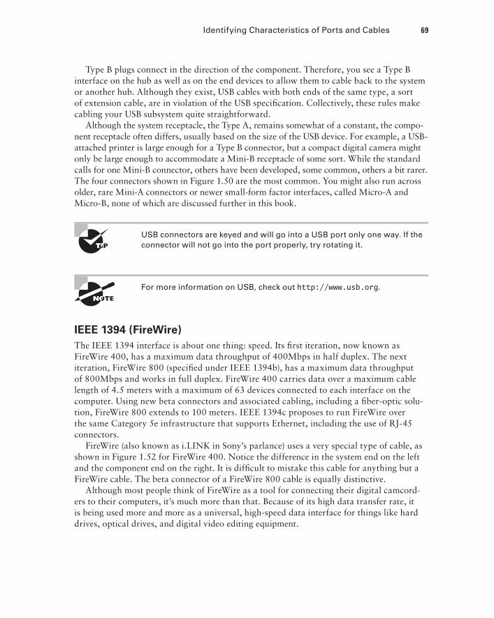
Identifying Characteristics of Ports and Cables 69
Type B plugs connect in the direction of the component. Therefore, you see a Type B interface on the hub as well as on the end devices to allow them to cable back to the system or another hub. Although they exist, USB cables with both ends of the same type, a sort of extension cable, are in violation of the USB specification. Collectively, these rules make cabling your USB subsystem quite straightforward.
Although the system receptacle, the Type A, remains somewhat of a constant, the compo-nent receptacle often differs, usually based on the size of the USB device. For example, a USB-attached printer is large enough for a Type B connector, but a compact digital camera might only be large enough to accommodate a Mini-B receptacle of some sort. While the standard calls for one Mini-B connector, others have been developed, some common, others a bit rarer. The four connectors shown in Figure 1.50 are the most common. You might also run across older, rare Mini-A connectors or newer small-form factor interfaces, called Micro-A and Micro-B, none of which are discussed further in this book.
USB connectors are keyed and will go into a USB port only one way. If the connector will not go into the port properly, try rotating it.
For more information on USB, check out .
IEEE 1394 (FireWire)
The IEEE 1394 interface is about one thing: speed. Its first iteration, now known as FireWire 400, has a maximum data throughput of 400Mbps in half duplex. The next iteration, FireWire 800 (specified under IEEE 1394b), has a maximum data throughput of 800Mbps and works in full duplex. FireWire 400 carries data over a maximum cable length of 4.5 meters with a maximum of 63 devices connected to each interface on the computer. Using new beta connectors and associated cabling, including a fiber-optic solu-tion, FireWire 800 extends to 100 meters. IEEE 1394c proposes to run FireWire over the same Category 5e infrastructure that supports Ethernet, including the use of RJ-45 connectors.
FireWire (also known as i.LINK in Sony’s parlance) uses a very special type of cable, as shown in Figure 1.52 for FireWire 400. Notice the difference in the system end on the left and the component end on the right. It is difficult to mistake this cable for anything but a FireWire cable. The beta connector of a FireWire 800 cable is equally distinctive.
Although most people think of FireWire as a tool for connecting their digital camcord-ers to their computers, it’s much more than that. Because of its high data transfer rate, it is being used more and more as a universal, high-speed data interface for things like hard drives, optical drives, and digital video editing equipment.
86498book.indb 69 7/22/09 5:37:55 AM
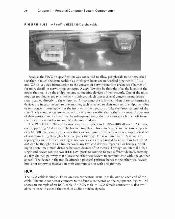
70 Chapter 1 Personal Computer System Components
F I GU R E 1.52 A FireWire (IEEE 1394) alpha cable
Because the FireWire specification was conceived to allow peripherals to be networked together in much the same fashion as intelligent hosts are networked together in LANs and WANs, a quick introduction to the concept of networking is in order; see Chapter 10 for more detail on networking concepts. A topology can be thought of as the layout of the nodes that make up the endpoints and connecting devices of the network. One of the most popular topologies today is the star topology, which uses a central concentrating device that is cabled directly to the endpoints. A tree structure is formed when these concentrating devices are interconnected to one another, each attached to their own set of endpoints. One or few concentrators appear at the first tier of the tree, sort of like the “root system” of the tree. These root devices are expected to carry more traffic than other concentrators because of their position in the hierarchy. In subsequent tiers, other concentrators branch off from the root and each other to complete the tree analogy.
The 1995 IEEE 1394 specification that is equivalent to FireWire 400 allows 1,023 buses, each supporting 63 devices, to be bridged together. This networkable architecture supports over 64,000 interconnected devices that can communicate directly with one another instead of communicating through a host computer the way USB is required to do. Star and tree topologies can be formed, as long as no two devices are separated by more than 16 hops. A hop can be thought of as a link between any two end devices, repeaters, or bridges, result-ing in a total maximum distance between devices of 72 meters. Through an internal hub, a single end device can use two IEEE 1394 ports to connect to two different devices, creating a daisy-chained pathway that allows the other two devices to communicate with one another as well. The device in the middle affords a physical pathway between the other two devices but is not otherwise involved in their communication with one another.
RCA
The RCA cable is simple. There are two connectors, usually male, one on each end of the cable. The male connector connects to the female connector on the equipment. Figure 1.53 shows an example of an RCA cable. An RCA male-to-RCA female connector is also avail-able; it’s used to extend the reach of audio or video signals.
86498book.indb 70 7/22/09 5:37:56 AM
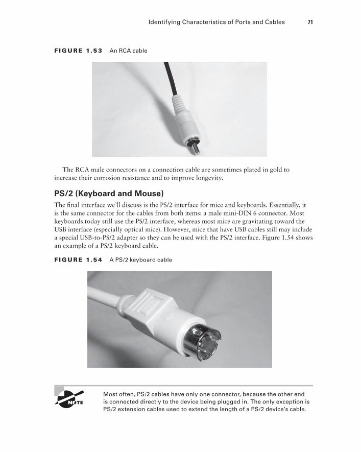
Identifying Characteristics of Ports and Cables 71
F I GU R E 1.5 3 An RCA cable
The RCA male connectors on a connection cable are sometimes plated in gold to increase their corrosion resistance and to improve longevity.
PS/2 (Keyboard and Mouse)
The final interface we’ll discuss is the PS/2 interface for mice and keyboards. Essentially, it is the same connector for the cables from both items: a male mini-DIN 6 connector. Most keyboards today still use the PS/2 interface, whereas most mice are gravitating toward the USB interface (especially optical mice). However, mice that have USB cables still may include a special USB-to-PS/2 adapter so they can be used with the PS/2 interface. Figure 1.54 shows an example of a PS/2 keyboard cable.
F I GU R E 1.5 4 A PS/2 keyboard cable
Most often, PS/2 cables have only one connector, because the other end is connected directly to the device being plugged in. The only exception is PS/2 extension cables used to extend the length of a PS/2 device’s cable.
86498book.indb 71 7/22/09 5:37:57 AM
72 Chapter 1 Personal Computer System Components
Identifying Purposes and Characteristics of Cooling SystemsIt’s a basic concept of physics: electronic components turn electricity into work and heat. The heat must be dissipated or the excess heat will shorten the life of the components. In some cases (like the CPU), the component will produce so much heat that it can destroy itself in a matter of seconds if there is not some way to remove this extra heat.
Most PCs use air-cooling methods to cool their internal components. With air cooling, the movement of air removes the heat from the component. Sometimes, large blocks of metal called heat sinks are attached to a heat-producing component in order to dissipate the heat more rapidly.
Fans
When you turn on a computer, you will often hear lots of whirring. Contrary to popular opinion, the majority of the noise isn’t coming from the hard disk (unless it’s about to go bad). Most of this noise is coming from the various fans inside the computer. Fans provide airflow within the computer.
Most PCs have a combination of these six fans:
Front intake fan This fan is used to bring fresh, cool air into the computer for cooling purposes.
Rear exhaust fan This fan is used to take hot air out of the case.
Power supply exhaust fan This fan is usually found at the back of the power supply and is used to cool the power supply. In addition, this fan draws air from inside the case into vents in the power supply. This pulls hot air through the power supply so that it can be blown out of the case. The front intake fan assists with this airflow. The rear exhaust fan supplements the power supply fan to achieve the same result outside of the power supply.
CPU fan This fan is used to cool the processor. Typically, this fan is attached to a large heat sink, which is in turn attached directly to the processor.
Chipset fan Some motherboard manufacturers replaced the heat sink on their onboard chipset with a heat sink and fan combination as the chipset became more advanced. This fan aids in the cooling of the onboard chipset (especially useful when overclocking).
Video card chipset fan As video cards get more complex and have higher performance, more video cards have cooling fans directly attached. Despite their name, these fans don’t attach to a chipset in the same sense as a chipset on a motherboard. The chipset here is the set of chips mounted on the adapter, including the graphics processing unit (GPU) and graphics memory.
86498book.indb 72 7/22/09 5:37:57 AM
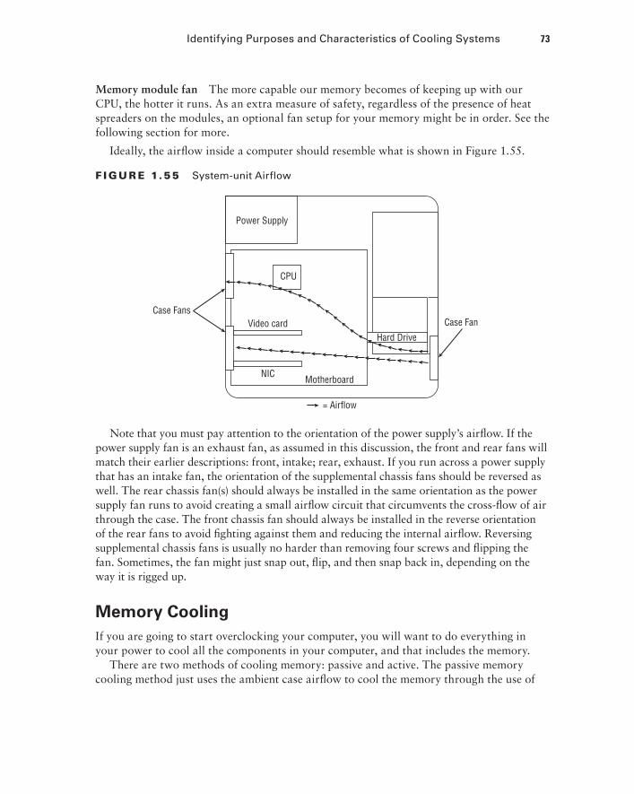
Identifying Purposes and Characteristics of Cooling Systems 73
Memory module fan The more capable our memory becomes of keeping up with our CPU, the hotter it runs. As an extra measure of safety, regardless of the presence of heat spreaders on the modules, an optional fan setup for your memory might be in order. See the following section for more.
Ideally, the airflow inside a computer should resemble what is shown in Figure 1.55.
F I GU R E 1.55 System-unit Airflow
Case FansCase Fan
Motherboard
= Airflow
NIC
Video card
CPU
Power Supply
Hard Drive
Note that you must pay attention to the orientation of the power supply’s airflow. If the power supply fan is an exhaust fan, as assumed in this discussion, the front and rear fans will match their earlier descriptions: front, intake; rear, exhaust. If you run across a power supply that has an intake fan, the orientation of the supplemental chassis fans should be reversed as well. The rear chassis fan(s) should always be installed in the same orientation as the power supply fan runs to avoid creating a small airflow circuit that circumvents the cross-flow of air through the case. The front chassis fan should always be installed in the reverse orientation of the rear fans to avoid fighting against them and reducing the internal airflow. Reversing supplemental chassis fans is usually no harder than removing four screws and flipping the fan. Sometimes, the fan might just snap out, flip, and then snap back in, depending on the way it is rigged up.
Memory Cooling
If you are going to start overclocking your computer, you will want to do everything in your power to cool all the components in your computer, and that includes the memory.
There are two methods of cooling memory: passive and active. The passive memory cooling method just uses the ambient case airflow to cool the memory through the use of
86498book.indb 73 7/22/09 5:37:57 AM
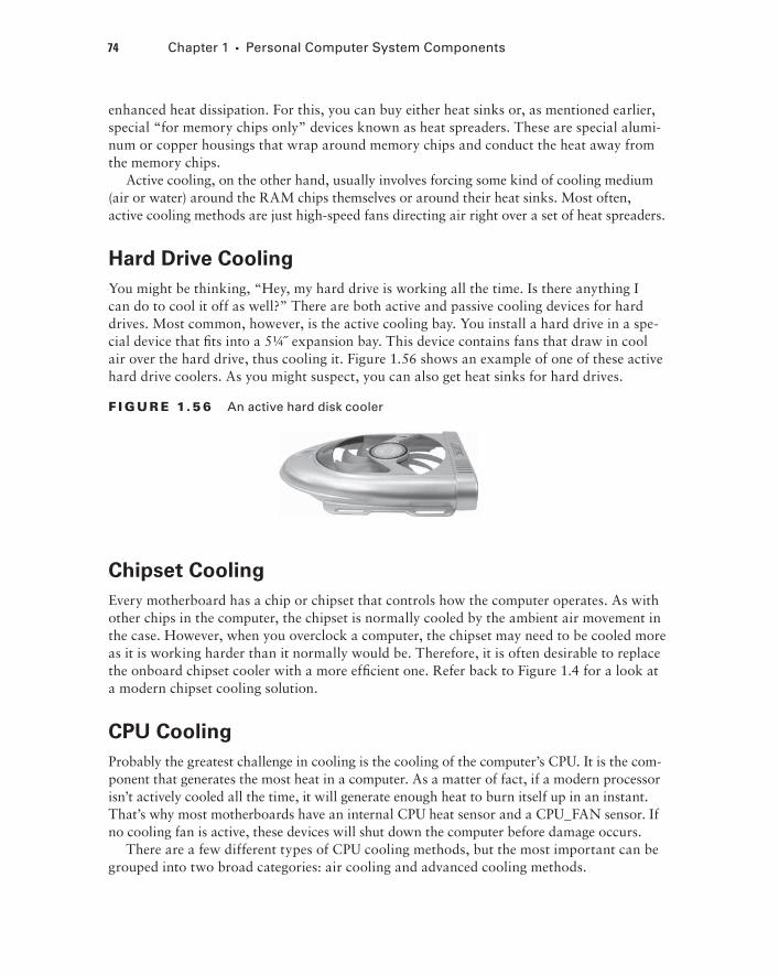
74 Chapter 1 Personal Computer System Components
enhanced heat dissipation. For this, you can buy either heat sinks or, as mentioned earlier, special “for memory chips only” devices known as heat spreaders. These are special alumi-num or copper housings that wrap around memory chips and conduct the heat away from the memory chips.
Active cooling, on the other hand, usually involves forcing some kind of cooling medium (air or water) around the RAM chips themselves or around their heat sinks. Most often, active cooling methods are just high-speed fans directing air right over a set of heat spreaders.
Hard Drive Cooling
You might be thinking, “Hey, my hard drive is working all the time. Is there anything I can do to cool it off as well?” There are both active and passive cooling devices for hard drives. Most common, however, is the active cooling bay. You install a hard drive in a spe-cial device that fits into a 5¼˝ expansion bay. This device contains fans that draw in cool air over the hard drive, thus cooling it. Figure 1.56 shows an example of one of these active hard drive coolers. As you might suspect, you can also get heat sinks for hard drives.
F I GU R E 1.56 An active hard disk cooler
Chipset Cooling
Every motherboard has a chip or chipset that controls how the computer operates. As with other chips in the computer, the chipset is normally cooled by the ambient air movement in the case. However, when you overclock a computer, the chipset may need to be cooled more as it is working harder than it normally would be. Therefore, it is often desirable to replace the onboard chipset cooler with a more efficient one. Refer back to Figure 1.4 for a look at a modern chipset cooling solution.
CPU Cooling
Probably the greatest challenge in cooling is the cooling of the computer’s CPU. It is the com-ponent that generates the most heat in a computer. As a matter of fact, if a modern processor isn’t actively cooled all the time, it will generate enough heat to burn itself up in an instant. That’s why most motherboards have an internal CPU heat sensor and a CPU_FAN sensor. If no cooling fan is active, these devices will shut down the computer before damage occurs.
There are a few different types of CPU cooling methods, but the most important can be grouped into two broad categories: air cooling and advanced cooling methods.
86498book.indb 74 7/22/09 5:37:58 AM
Identifying Purposes and Characteristics of Cooling Systems 75
Air Cooling
The parts inside most computers are cooled by air moving through the case. The CPU is no exception. However, because of the large amount of heat produced, the CPU must have (proportionately) the largest surface area exposed to the moving air in the case. Therefore, the heat sinks on the CPU are the largest of any inside the computer.
This fan often blows air down through the body of the heat sink to force the heat into the ambient internal air where it can join the airflow circuit for removal from the case. However, the latest trend, in support of high-end processors, is a redesign of the classic heat sink. The heat sink extends up farther, using radiator-type fins, and the fan is placed at a right angle and to the side of the heat sink. This design moves the heat away from the heat sink imme-diately, instead of pushing the air down through the heat sink. CPU fans can be purchased that have an adjustable rheostat to allow you to dial in as little airflow as you need, aiding in noise reduction but potentially leading to accidental overheating.
It should be noted that the highest-performing CPU coolers use copper plates in direct contact with the CPU. They also use high-speed and high-CFM cooling fans to dissipate the heat produced by the processor. CFM is short for cubic feet per minute, an airflow measurement of the volume of air that passes by a stationary object per minute.
Most new CPU heat sinks use tubing to transfer heat away from the CPU. With any cooling system, the more surface area exposed to the cooling method, the better the cool-ing. Plus, the heat pipes can be used to transfer heat to a location away from the heat source before cooling. This is especially useful in small-form factor cases and laptops, where open space is limited.
With advanced heat sinks and CPU cooling methods like this, it is important to improve the thermal transfer efficiency as much as possible. To that end, cooling engineers came up with a compound that helps to bridge the extremely small gaps between the CPU and the heat sink, which avoids superheated pockets of air that can lead to focal damage of the CPU. This product is known as thermal transfer compound or simply thermal compound (alternatively, thermal grease or thermal paste) and can be bought in small tubes. Single-use tubes alleviate the guessing involved with how much you should apply. Watch out, though; this stuff makes quite a mess and doesn’t want to come off your fingers very easily.
Apply the compound by placing a bead in the center of the heat sink, not on the CPU because some heat sinks don’t cover the entire CPU package. That might sound like an issue, but some CPUs don’t have heat-producing components all the way out to the edges. Some CPUs even have a raised area directly over where the silicon die is within the pack-aging, resulting in a smaller contact area between the components. You should apply less than you think you need because the pressure of attaching the heat sink to the CPU will spread the compound across the entire surface in a very thin layer. It’s advisable to use a clean, lint-free applicator of your choosing to spread the compound around a bit as well, just to get the spreading started. You don’t need to concern yourself with spreading it too thoroughly or too neatly because the pressure applied during attachment will equalize the compound quite well. During attachment, watch for oozing compound around the edges, clean it off immediately, and use less next time.
86498book.indb 75 7/22/09 5:37:58 AM
76 Chapter 1 Personal Computer System Components
Improving and Maintaining CPU Cooling
In addition to using thermal compound, you can enhance the cooling efficiency of a CPU heat sink by lapping the heat sink, which smoothes the mating surface using a very fine sanding element, about 1000-grit in the finishing stage. Some vendors of the more expensive heat sinks will offer this service as an add-on.
If your CPU has been in service for an extended period of time, perhaps three years or more, it is a smart idea to remove the heat sink and old thermal compound and then apply fresh thermal compound and reattach the heat sink. Be careful, though; if your thermal paste has already turned into thermal “glue,” you can wrench the processor right out of the socket, even with the release mechanism locked in place. Invariably, this damages the pins on the chip.
Counterintuitively, perhaps, you can remove a released heat sink from the processor by gently rotating the heat sink to break the paste’s seal. If the CPU has risen in the socket already, however, this would be an extremely bad idea. Sometimes, after you realize that the CPU has risen a bit and that you need to release the mechanism holding it in to reseat it, you find the release arm is not accessible with the heat sink in place. This is an unfortunate predicament that will present plenty of opportunity to learn.
If you’ve ever installed a brand-new heat sink onto a CPU, you’ve most likely used ther-mal compound or the thermal compound patch that was already applied to the heat sink for you. If your new heat sink has a patch of thermal compound preapplied, don’t add more. If you ever remove the heat sink, don’t try to reuse the patch or any other form of thermal compound. Clean it all off and start fresh.
Advanced CPU Cooling Methods
Advancements in air cooling have led to products like the Scythe Ninja 2, which is a stack of thin aluminum fins with copper tubing running up through them. Some of the hottest-running CPUs can be passively cooled with a device like this, using only the existing air-movement scheme from your computer’s case. Adding a fan to the side, however, adds to the cooling efficiency, but also to the noise level.
In addition to standard and advanced air-cooling methods, there are other methods of cooling a CPU (and other chips as well). These methods might appear somewhat unortho-dox but often deliver extreme results.
These methods can also result in permanent damage to your computer, so try them at your own risk.
86498book.indb 76 7/22/09 5:37:58 AM
Identifying Purposes and Characteristics of Cooling Systems 77
Liquid Cooling
Liquid cooling is a technology whereby a special water block is used to conduct heat away from the processor (as well as from the chipset). Water is circulated through this block to a radiator, where it is cooled.
The theory is that you could achieve better cooling performance through the use of liquid cooling. For the most part, this is true. However, with traditional cooling methods (which use air and water), the lowest temperature you can achieve is room temperature. Plus, with liquid cooling, the pump is submerged in the coolant (generally speaking), so as it works, it produces heat, which adds to the overall liquid temperature.
The main benefit to liquid cooling is silence. There is only one fan needed: the fan on the radiator to cool the water. So a liquid-cooled system can run extremely quietly.
Liquid cooling, while more efficient than air cooling and much quieter, has its drawbacks. Most liquid-cooling systems are more expensive than supplemental fan sets, and require less familiar components, such as reservoir, pump, water block(s), hose, and radiator.
The relative complexity of installing liquid cooling systems, coupled with the perceived danger of liquids in close proximity to electronics, leads most computer owners to consider liquid cooling a novelty or a liability. The primary market for liquid cooling is the high-performance niche that engages in overclocking to some degree. However, developments in active air cooling, including extensive piping of heat away from the body of the heat sink, have kept advanced cooling methods out of the forefront.
Heat Pipes
Heat pipes are closed systems that employ some form of tubing filled with a liquid suitable for the applicable temperature range. Pure physics are used with this technology to achieve cooling to ambient temperatures; no outside mechanism is used. One end of the heat pipe is heated by the component being cooled. This causes the liquid at the heated end to evaporate and increase the relative pressure at that end of the heat pipe with respect to the cooler end. This pressure imbalance causes the heated vapor to equalize the pressure by migrating to the cooler end, where the vapor condenses and releases its heat, warming the nonheated end of the pipe. The cooler environment surrounding this end transfers the heat away from the pipe by convection. The condensed liquid drifts to the pipe’s walls and is drawn back to the heated end of the heat pipe by gravity or by a wicking material or texture that lines the inside of the pipe. Once the liquid returns, the process repeats.
Peltier Cooling Devices
Water- and air-cooling devices are extremely effective by themselves, but they are more effective when used with a device known as a Peltier cooling element. These devices, also known as thermoelectric coolers (TECs), facilitate the transfer of heat from one side of the element, made of one material, to the other side, made of a different material. Thus, they have a hot side and a cold side. The cold side should always be against the CPU sur-face, and optimally, the hot side should be mated with a heat sink or water block for heat dissipation. Consequently, TECs are not meant to replace air-cooling mechanisms but to complement them.
86498book.indb 77 7/22/09 5:37:59 AM
78 Chapter 1 Personal Computer System Components
One of the downsides to TECs is the likelihood of condensation because of the sub-ambient temperatures these devices produce. Closed-cell foams can be used to guard against damage from condensation.
Phase-Change Cooling
There is one new type of PC cooling that is just starting to be seen: phase-change cooling. With this type of cooling, the cooling effect from the change of a liquid to a gas is used to cool the inside of a PC. It is a very expensive method of cooling, but it does work. Most often, external air-conditioner-like pumps, coils, and evaporators cool the coolant, which is sent, ice cold, to the heat sink blocks on the processor and chipset. Think of it as a water-cooling system that chills the water below room temperature. It is possible to get CPU temps in the range of –4°F (–20°C). Normal CPU temperatures hover between 104°F and 122°F (40°C and 50°C).
The major drawback to this method is that in higher-humidity conditions, condensation can be a problem. The moisture from the air condenses on the heat sink and can run off onto and under the processor, thus shorting out the electronics. Designers of phase-change cooling systems offer solutions to help ensure this isn’t a problem. Products in the form of foam; silicone adhesive; and greaseless, non-curing adhesives are available to seal the surface and perimeter of the processor. Additionally, manufacturers sell gaskets and shims that correspond to specific processors, all designed to protect your delicate and expensive components from damage.
Liquid Nitrogen and Helium Cooling
In the interest of completeness, there is a novel approach to super-cooling processors that is ill-advised under all but the most extreme circumstances. By filling a vessel placed over the component to be cooled with a liquid form of nitrogen or, for an even more intense effect, helium, temperatures from –100 to –240 degrees Celsius can be achieved. The results are short-lived and only useful in overclocking with a view to setting records. The processor is not likely to survive the incident, due to the internal stress from the extreme temperature changes.
SummaryIn this chapter, we took a tour of the system components of a PC. You learned about some of the elements that make up a PC. You’ll learn about others in the next two chapters. In addition, we discussed common peripheral ports and cables and their appearance. Finally, you learned about the various methods used for cooling a PC. You also saw what many of these items look like and how they function.
86498book.indb 78 7/22/09 5:37:59 AM
Exam Essentials 79
Exam Essentials
Know the types of system boards. Know the characteristics of and differences between ATX, micro ATX, NLX, and BTX motherboards.
Know the components of a motherboard. Be able to describe motherboard components, such as chipsets, expansion slots, memory slots, and external cache; CPU and processor slots or sockets; power connectors; onboard disk drive connectors; keyboard connectors; peripheral ports and connectors; BIOS (firmware) chips; CMOS batteries; jumpers; and DIP switches.
Understand the purposes and characteristics of processors. Be able to discuss the different processor packaging, old and new, and know the meaning of the terms hyperthreading, multi-core, throttling, microcode, overclocking, cache, speed, and system bus width.
Understand the purposes and characteristics of memory. Know about the characteristics that set the various types of memory apart from one another. This includes the actual types of memory, such as DRAM, which includes several varieties, SRAM, ROM, and CMOS, as well as memory packaging, such as SIMMs, DIMMs, RIMMs, SODIMMS, and MicroDIMMs. Also have a firm understanding of the different levels of cache memory as well as its purpose in general.
Understand the purposes and characteristics of adapter cards and their ports and cables. Familiarize yourself with the variety of expansion cards and integrated components in today’s computer systems, as well as the ports they use and any cables that connect to external devices.
Understand the purposes and characteristics of cooling systems. Know the different ways that internal components can be cooled and how overheating can be prevented.
86498book.indb 79 7/22/09 5:37:59 AM
80 Chapter 1 Personal Computer System Components
Review Questions
1. Which computer component contains all the circuitry necessary for other components or devices to communicate with one another?
A. Motherboard
B. Adapter card
C. Hard drive
D. Expansion bus
2. Which packaging is used for DDR SDRAM memory?
A. 168-pin DIMM
B. 72-pin SIMM
C. 184-pin DIMM
D. RIMM
3. What memory chips would you find on a stick of PC3-16000?
A. DDR-2000
B. DDR3-2000
C. DDR3-16000
D. PC3-2000
4. Which motherboard design style is most widely implemented?
A. ATX
B. AT
C. Baby AT
D. NLX
5. Which motherboard socket type is used on the Pentium 4 chip?
A. Slot 1
B. Socket A
C. Socket 370
D. Socket 478
6. Which of the following is a socket technology that is designed to ease insertion of modern CPUs?
A. Socket 479
B. ZIF
C. LPGA
D. SPGA
86498book.indb 80 7/22/09 5:37:59 AM
Review Questions 81
7. Which of the following is not controlled by the Northbridge?
A. PCIe
B. SATA
C. AGP
D. Cache memory
8. Which of the following is used to store data and programs for repeated use? Information can be added and deleted at will, and it does not lose its data when power is removed.
A. Hard drive
B. RAM
C. Internal cache memory
D. ROM
9. Which motherboard socket type is used with the AMD Athlon XP?
A. Slot 1
B. Socket A
C. Socket 370
D. Socket 478
10. You want to plug a keyboard into the back of a computer. You know that you need to plug the keyboard cable into a PS/2 port. Which style of port is the PS/2?
A. RJ-11
B. DE9
C. DIN 5
D. Mini-DIN 6
11. Which of the following are the numbers of pins that can be found on DIMM modules used in desktop motherboards? (Choose three.)
A. 168
B. 180
C. 184
D. 200
E. 204
F. 232
G. 240
12. What is the maximum speed of USB 2.0 in Mbps?
A. 1.5
B. 12
C. 60
D. 480
86498book.indb 81 7/22/09 5:37:59 AM
82 Chapter 1 Personal Computer System Components
13. Which of the following standards are specified by IEEE 1284? (Choose two.)
A. SPP
B. RS-232
C. EPP
D. ECP
E. FireWire
F. USB
14. What peripheral port type was originally developed by Apple and is currently the optimal interface for digital video transfers?
A. DVD
B. USB
C. IEEE 1394
D. IEEE 1284
15. What peripheral port type is expandable using a hub, operates at 1.5MBps, and is used to connect various devices (from printers to cameras) to PCs?
A. DVD 1.0
B. USB 1.1
C. IEEE 1394
D. IEEE 1284
16. Which peripheral port type was designed to transfer data at high speeds over a D-sub interface?
A. DVD
B. USB
C. IEEE 1394
D. IEEE 1284
17. Which motherboard form factor places expansion slots on a special riser card and is used in low-profile PCs?
A. AT
B. Baby AT
C. ATX
D. NLX
18. Which Intel processor type might be mounted on a SECC for motherboard installation?
A. Athlon
B. 486
C. Pentium
D. Pentium II
86498book.indb 82 7/22/09 5:37:59 AM

Review Questions 83
19. You have just purchased a motherboard that has an LGA775 socket for an Intel Pentium 4 processor. What type of memory modules will you need for this motherboard?
A. DIP
B. SIMM
C. RIMM
D. DIMM
20. What type of expansion slot is preferred today for high-performance graphics adapters?
A. AGP
B. PCIe
C. PCI
D. ISA
86498book.indb 83 7/22/09 5:37:59 AM
84 Chapter 1 Personal Computer System Components
Answers to Review Questions
1. A. The spine of the computer is the system board, otherwise known as the motherboard. On the motherboard you will find the CPU, underlying circuitry, expansion slots, video components, RAM slots, and various other chips.
2. C. DDR SDRAM is manufactured on a 184-pin DIMM. DIMMs with 168 pins were used for SDR SDRAM. The SIMM is the predecessor to the DIMM, on which SDRAM was never deployed. RIMM is the Rambus proprietary competitor for the DIMM that carries DRDRAM instead of SDRAM.
3. B. Remember the 8:1 rule. Modules greater than, but not including, SDR SDRAM are named with a number 8 times larger than the number used to name the chips on the module. The initials PC are used to describe the module, the initials DDR for the chips, and a number to represent the level of DDR. The lack of a number represents DDR, as long as the associated number is greater than 133. Otherwise, you’re dealing with SDR. This means that PC3-16000 modules are DDR3 modules and are populated with chips named DDR3 and a number that is 1⁄8 of the module’s numeric code: 2000.
4. A. Although all the motherboard design styles listed are in use today, the ATX motherboard style (and its derivatives) is the most popular design.
5. D. Most Pentium 4 chips use the Socket 478 motherboard CPU socket, although not exclusively. Nevertheless, no other option listed is used for these processors.
6. B. ZIF sockets are designed with a locking mechanism that, when released, alleviates the resistance of the socket to receiving the pins of the chip being inserted. Make sure you know your socket types so that the appearance of a specific model, such as Socket 479, in a question like this does not distract you from the correct answer. Only LGA would be another acceptable answer to this question because, with a lack of pin receptacles, there is no insertion resistance. However, no other pin-layout format, such as SPGA, addresses issues with inserting chips. LPGA might have evoked an image of LGA, leading you to that answer, but that term means nothing outside of the golfing community.
7. B. The Northbridge is in control of the local-bus components that share the clock of the frontside bus. SATA and all other drive interfaces do not share this clock and are controlled by the Southbridge.
8. A. A hard drive stores data on a magnetic medium, which does not lose its information after the power is removed, and which can be repeatedly written to and erased.
9. B. The Socket A (remember A for AMD) motherboard socket is used primarily with AMD processors, including the Athlon XP.
10. D. A PS/2 port is also known as a mini-DIN 6 connector.
86498book.indb 84 7/22/09 5:37:59 AM
Answers to Review Questions 85
11. A, C, G. DIMMs used in desktop-motherboard applications have one of three possible pin counts. SDR SDRAM is implemented on 168-pin modules. DDR SDRAM and 16-bit RIMMs are implemented on 184-pin modules. DDR2 and DDR3 are implemented on 240-pin modules with different keying. Dual-channel RIMM modules have 232 pins. Modules with 200 and 204 pins are used in the SODIMM line, and there are no modules with 180 pins.
12. D. The USB 2.0 spec provides for a maximum speed of 480 megabits per second (Mbps—not megabytes per second, or MBps).
13. C, D. Bidirectional parallel ports can both transmit and receive data. EPP and ECP are IEEE-1284 standards that were designed to transfer data at high speeds in both directions so that devices could return status information to the system. The standard parallel port only transmits data out of the computer. It cannot receive data. FireWire is specified by IEEE 1394. IEEE 1284 does not specify serial protocols, such as RS-232 and USB.
14. C. The 1394 standard provides for greater data transfer speeds and the ability to send memory addresses as well as data through a serial port.
15. B. USBs are used to connect multiple peripherals to one computer through a single port. They support data transfer rates as high as 12Mbps, or 1.5MBps (for USB 1.1, which is the option listed here).
16. D. IEEE 1284 standard defines the ECP parallel port to use a DMA channel and the buffer to be able to transfer data at high speeds to printers.
17. D. The NLX form factor places expansion slots on a special riser card and is used in low-profile PCs.
18. D. The unique thing about the Pentium II is that it was attached to a single edge contact cartridge (SECC) for insertion into the motherboard, instead of the standard PGA package. Athlon is an AMD processor, the early version of which was slot-based, but not considered SECC, in any event.
19. D. Pentium 4 processors are always mated with memory mounted on DIMMs.
20. B. Although technically all slots listed could be used for video adapters, PCIe excels when compared to the other options and offers technologies, such as SLI, which only make PCIe’s advantage more noticeable.
86498book.indb 85 7/22/09 5:38:00 AM