thermal vibration analysis on single layer graphene embedded in elastic medium
Upload
vlad-voicuCategory
view
235download
0
8/13/2019 Sample Analysis - Graphene Sample Analysis
http://slidepdf.com/reader/full/sample-analysis-graphene-sample-analysis 1/5
TelFaxEmail
+44 (0) 1453 523800+44 (0) 1453 [email protected]
Renishaw plcSpectroscopy Products DivisionOld Town, Wotton-under-Edge,Gloucestershire GL12 7DWUnited Kingdom www.renishaw.com
Graphene sample analysis Ref: 44640Overview
A graphene sample was analysed using a 514 nm laser excitation source to estimate the thickness of thegraphene layer as well as to assess the uniformity of the layer
Spot measurements
SynchroScan™ was used to generate seamless, high resolution spectra over a wide and user definablespectral range. Experimental conditions are specified in Table 1.
Table 1. Experimental conditions
Model inVia Reflex Raman microscopeExcitation 514 nm (Ar +)Objective 50x N plan (diffraction limited)Scan type SynchroScan™Grating 1800 lines/mmScan range 1000 cm -1 to 3200 cm -1
Acquisition time 20 s
Figure 1. Raman spectra taken from (a) the centre of the sample, (b) 1 mm from the centre of the sample and (c) 3 mmfrom the centre of the sample. The graphene G, 2D and D are labelled and SiC modes are denoted with *.
(a)
(c)
(b)
2D
G
D
*
* *
D+G

8/13/2019 Sample Analysis - Graphene Sample Analysis
http://slidepdf.com/reader/full/sample-analysis-graphene-sample-analysis 2/5
Graphene Sample Analysis
2
Figure 1 illustrates the typical spectra obtained from spot measurements on the samples using the conditionsspecified in Table 1. The characteristic modes for graphene, G-peak, 2D-peak and D-peak as well as the SiCmodes are labelled.
The relative intensity of the G and SiC mode at ~1550 can be used to qualitatively assess the thickness ofthe graphene layer, with thicker layers having a higher ratio. This implies that spectrum (c) originates frommultilayer graphene, a fact which is further reinforced by the shift of the 2D peak at ~2700 cm -1 to a lowerwave number (closer to that of freestanding graphene). The graphene layer thickness has been shown toeffect the shape of the 2D-peak in graphene obtained by micromechanical cleavage of graphite ( A. C. Ferrariet al., PRL 97, 187401 (2006) ). Ni et al. (PHYSICAL REVIEW B, 77 , 115416 (2008 )) have characterisedmonolayer graphene samples on SiC using Raman spectroscopy. The peak width and position of the 2Dpeak from spectra (a) and (b) is consistent with that from 1-3 monolayers of graphene. A calibrationmeasurement of a sample with known thickness is needed To determine the precise number of graphene
layers.
StreamLine™ imaging measurements
A calibration measurement of a sample with known thickness is needed to analyse the uniformity of thegraphene film mapping measurements were taken using StreamLine™ imaging. This enabled a high spatialresolution map of the target area to be measured quickly. StreamLine™ uses a laser line instead of a spot,for graphene this give the added benefit of lowering the laser power density on the sample, reducing anyeffects of laser heating. The measurement configuration used for these measurements is given in Table 2.By extracting the 2D peak width from the measured data the thickness of the graphene layer can be assesson a large scale. Local stress information can be obtained by investigating the peak position of both the Gand 2D phonon modes.
Table 2. Experimental conditions
Model inVia Reflex Raman microscopeExcitation 514 nm (Ar +)Objective 50x N plan (diffraction limited)Scan type Streamline™Grating 1800 lines/mmScan range 1260 cm -1 to 2930 cm -1
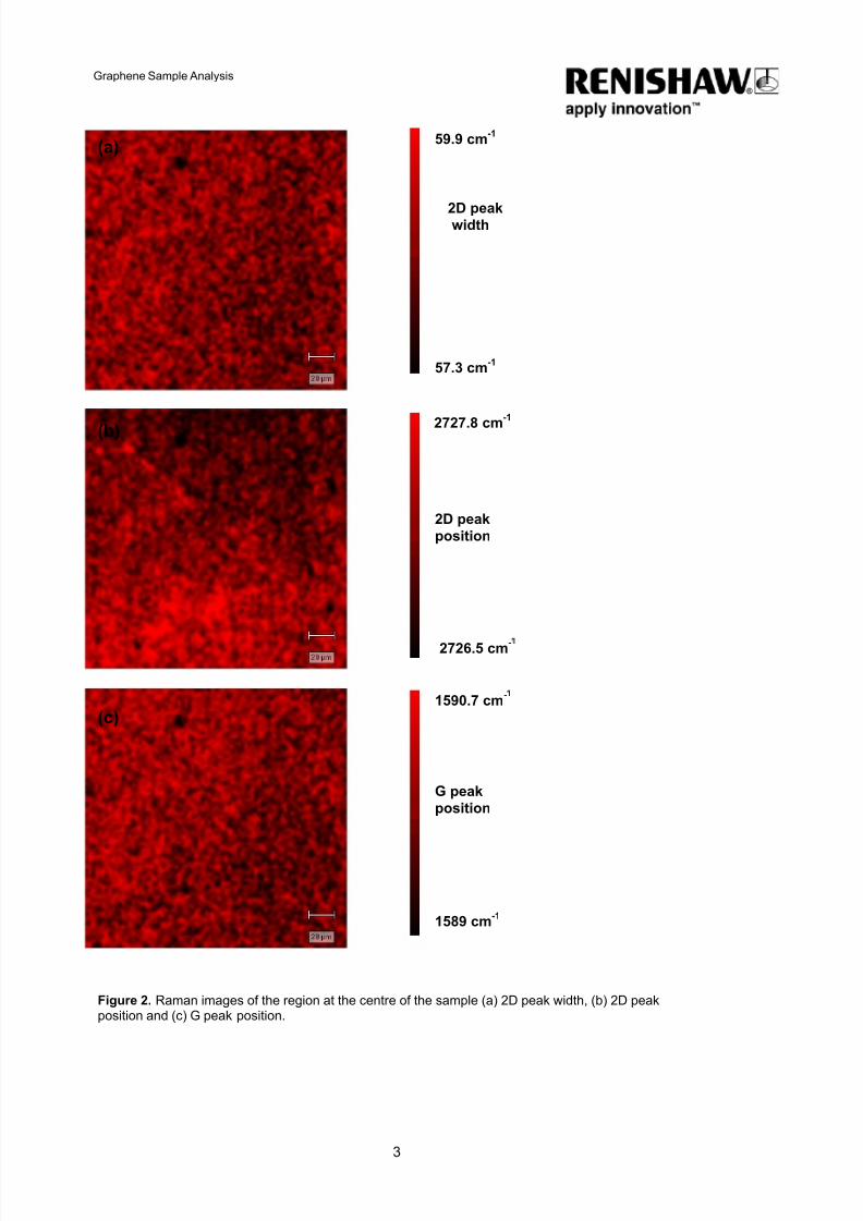
Figure 2 contains Raman map images of a 200 µm x 200 µm area lying at the centre of the sampleconsisting of 6162 points, illustrating the uniformity of the graphene in this region.Figure 3 consists of Raman images taken from a longer region with the top right hand corner of the maplocated 100 µm to the left of the area in Figure 2.
8/13/2019 Sample Analysis - Graphene Sample Analysis
http://slidepdf.com/reader/full/sample-analysis-graphene-sample-analysis 3/5
Graphene Sample Analysis
3
Figure 2. Raman images of the region at the centre of the sample (a) 2D peak width, (b) 2D peakposition and (c) G peak position.
59.9 cm -1
57.3 cm -1
(a)
2727.8 cm-1
2726.5 cm -
(b)
1590.7 cm -
1589 cm -1
(c)
2D peakwidth
2D peakposition
G peakposition

8/13/2019 Sample Analysis - Graphene Sample Analysis
http://slidepdf.com/reader/full/sample-analysis-graphene-sample-analysis 4/5
Graphene Sample Analysis
4
58 cm -
54..3 cm -1
2D peakwidth
1590.7 cm -
1583.9 cm -1
G peakposition
Figure 3. Raman images of a region near the centre of thesample (a) 2D peak width, (b) 2D peak position and (c) G
peak position.

8/13/2019 Sample Analysis - Graphene Sample Analysis
http://slidepdf.com/reader/full/sample-analysis-graphene-sample-analysis 5/5
Graphene Sample Analysis
5
For both the areas mapped the 2D peak width is consistent with that of a few monolayers of graphene, thesmall variation in peak width over the area suggests that the sample is of uniform thickness but contains adistribution of defects. The region in the bottom right of Figure 3 shows a distinct variation in G peak positionin relation to the rest of the area suggesting a variation in local stress in this region. Ni et al. determined thestress coefficient for graphene on SiC to be 7.47 cm -1/GPa giving a maximum stress variation in Figure 3 of~0.9 GPa.
Conclusion
Raman spectroscopy has been used to assess the thickness and quality of graphene grown on a SiCsubstrate. The use of the Renishaw SynchroScan™ spectral collection method allowed spectrum to becollected in one go without changing optics and at the highest spectral resolution. This is important as theRaman bands specific to Graphene lie over a large spectral range ~1500cm -1 and measurements of all thesebands are required to gain maximum material information.
StreamLine™ Raman imaging was used to estimate the thickness of graphene and uniformity of thegraphene layer quickly over larger length scales using a laser line enabling a much lower laser power densityto be used on the sample reducing any effects of laser heating.