SAA7826 CD audio decoder, digital servo and filterless DAC ... Sheets/NXP PDFs/SAA7826_2.pdf ·...
89
DATA SHEET Product specificationSupersedes data of 2003 Aug 04 2003 Oct 01 INTEGRATED CIRCUITS SAA7826 CD audio decoder, digital servo and filterless DAC with integrated pre-amp and laser control
Transcript of SAA7826 CD audio decoder, digital servo and filterless DAC ... Sheets/NXP PDFs/SAA7826_2.pdf ·...
DATA SHEET
Product specificationSupersedes data of 2003 Aug 04 2003 Oct 01
INTEGRATED CIRCUITS
SAA7826CD audio decoder, digital servo andfilterless DAC with integratedpre-amp and laser control
2003 Oct 01 2
Philips Semiconductors Product specification
CD audio decoder, digital servo and filterlessDAC with integrated pre-amp and laser control
SAA7826
CONTENTS
1 FEATURES
2 GENERAL DESCRIPTION
3 ORDERING INFORMATION
4 QUICK REFERENCE DATA
5 BLOCK DIAGRAM
6 PINNING
7 FUNCTIONAL DESCRIPTION
7.1 Data acquisition and HF data path7.2 Decoder part7.2.1 Principle operating modes of the decoder7.2.2 Decoder speed and crystal frequency7.2.3 Lock-to-disc mode7.2.4 Standby modes7.3 Crystal oscillator7.4 Data slicer and bit clock regenerator7.5 DC offset cancellation7.5.1 Offset cancellation7.5.2 Reading back the DC offset value7.6 Demodulator7.6.1 Frame sync protection7.6.2 EFM demodulation7.7 Subcode data processing7.7.1 Q-channel processing7.7.2 EIAJ 3 and 4-wire subcode (CD graphics)
interface7.7.3 V4 subcode interface7.7.4 CD text interface7.8 FIFO and error correction7.8.1 Flags output (CFLG)7.9 Audio functions7.9.1 De-emphasis and phase linearity7.9.2 Digital oversampling filter7.9.3 Concealment7.9.4 Mute, full-scale, attenuation and fade7.9.5 Peak detector7.10 Audio DAC interface7.10.1 Internal dynamic element matching
digital-to-analog converter7.10.2 External DAC interface7.11 EBU interface7.11.1 Format7.12 KILL features7.12.1 The KILL circuit7.12.2 Silence injection7.13 Audio features off7.14 The versatile pins interface7.15 Spindle motor control7.15.1 Motor output modes7.15.2 Spindle motor operating modes
7.15.3 Loop characteristics7.15.4 FIFO overflow7.16 Servo part7.16.1 Diode signal processing7.16.2 Signal conditioning7.16.3 Focus servo system7.16.4 Radial servo system7.16.5 Off-track counting7.16.6 Track counting modes7.16.7 Defect detection7.16.8 Off-track detection7.16.9 High-level features7.16.10 Driver interface7.16.11 Laser interface7.17 Microcontroller interface7.17.1 Microcontroller interface (4-wire bus mode)7.17.2 Microcontroller interface (I2C-bus mode)7.17.3 Decoder and shadow registers7.17.4 Summary of functions controlled by decoder
registers 0 to F7.17.5 Summary of functions controlled by shadow
registers7.17.6 Summary of servo commands7.17.7 Summary of servo command parameters
8 SUMMARY OF SERVO COMMANDPARAMETERS VALUES
9 LIMITING VALUES
10 CHARACTERISTICS
11 OPERATING CHARACTERISTICS(SUBCODE INTERFACE TIMING)
12 OPERATING CHARACTERISTICS (I2S-BUSTIMING)
13 OPERATING CHARACTERISTICS(MICROCONTROLLER INTERFACE TIMING)
14 APPLICATION INFORMATION
15 PACKAGE OUTLINE
16 SOLDERING
16.1 Introduction to soldering surface mountpackages
16.2 Reflow soldering16.3 Wave soldering16.4 Manual soldering16.5 Suitability of surface mount IC packages for
wave and reflow soldering methods
17 DATA SHEET STATUS
18 DEFINITIONS
19 DISCLAIMERS
20 PURCHASE OF PHILIPS I2C COMPONENTS
2003 Oct 01 3
Philips Semiconductors Product specification
CD audio decoder, digital servo and filterlessDAC with integrated pre-amp and laser control
SAA7826
1 FEATURES
• Decoder and servo parts are based upon the SAA732Xdesign (the original features are maintained)
• Software compatibility is maintained with the SAA732Xby using a similar register structure (new features arecontrolled from new shadow registers)
• 1×, 2× and 4× speed
• LF (servo) signals converted to digital representationsby 6 oversampling bitstream ADCs
• HF part summed from signals D1 to D4 and convertedto a digital signal by a data slicer
• On-chip buffering and filtering of the diode signals fromthe mechanism for signal optimization
• Selectable DC offset cancellation of quiescentmechanism voltages and dark currents
• On-chip laser power control (up to 120 mA)
• Laser on/off control, including ‘soft’ start control (zero tonominal power in 1 ms)
• Monitor control and feedback circuit to maintain nominaloutput power throughout laser life
• Dynamic element matching DAC with minimum externalcomponents
• DAC performance of −80 dB Total HarmonicDistortion + Noise (THD + N) and 90 dB Signal-to-NoiseRatio (S/N) A-weighted
• Separate left and right channel digital silence detectionavailable on the KILL pins
• Digital silence detection on internal data and loopback(external) data
• 5 versatile pins, 2 inputs and 3 outputs
• Integrated CD text decoder with separatemicrocontroller interface
• Dedicated 4 MHz or 12 MHz clock output formicrocontroller (configurable)
• Configured for N-sub monitor diode
• On-chip clock multiplier allows the use of an8.4672 MHz crystal or ceramic resonator
• The M1 version has an EBU mute function which allowsindependent muting of data being transmitted over theEBU interface whilst maintaining the SPDIF framestructure.
2 GENERAL DESCRIPTION
This document covers versions M0 and M1 of the CDaudio decoder IC.
The SAA7826 is a CD audio decoder IC which combinesthe function of the SAA732X IC with the pre-amplifier andlaser control functions previously found in the TZA102XIC. The design is intended to reduce the externalcomponent count and hence the Bill Of Material (BOM).
Supply of this Compact Disc IC does not convey animplied license under any patent right to use this IC in anyCompact Disc application.
2003 Oct 01 4
Philips Semiconductors Product specification
CD audio decoder, digital servo and filterlessDAC with integrated pre-amp and laser control
SAA7826
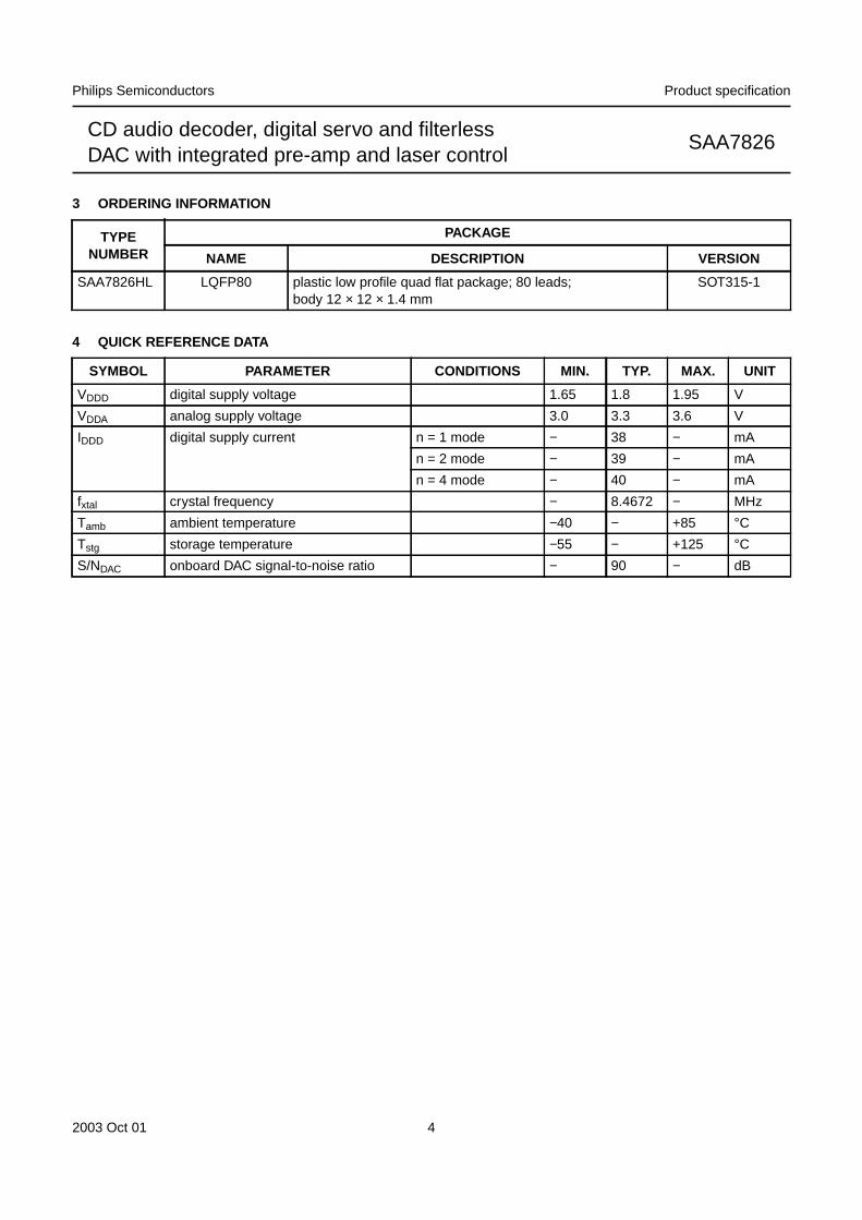
3 ORDERING INFORMATION
4 QUICK REFERENCE DATA
TYPENUMBER
PACKAGE
NAME DESCRIPTION VERSION
SAA7826HL LQFP80 plastic low profile quad flat package; 80 leads;body 12 × 12 × 1.4 mm
SOT315-1
SYMBOL PARAMETER CONDITIONS MIN. TYP. MAX. UNIT
VDDD digital supply voltage 1.65 1.8 1.95 V
VDDA analog supply voltage 3.0 3.3 3.6 V
IDDD digital supply current n = 1 mode − 38 − mA
n = 2 mode − 39 − mA
n = 4 mode − 40 − mA
fxtal crystal frequency − 8.4672 − MHz
Tamb ambient temperature −40 − +85 °CTstg storage temperature −55 − +125 °CS/NDAC onboard DAC signal-to-noise ratio − 90 − dB
2003 Oct 01 5
Philips Semiconductors Product specification
CD audio decoder, digital servo and filterlessDAC with integrated pre-amp and laser control
SAA7826
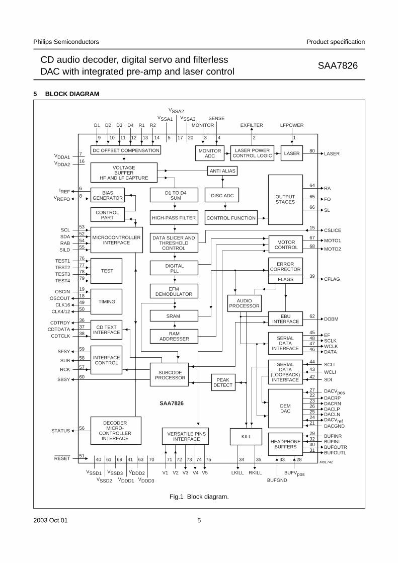
5 BLOCK DIAGRAM
handbook, full pagewidth
DC OFFSET COMPENSATION
IREF
SCLSDARABSILD
VREFO
D1
9
6
VDDA17
VDDA216
8
525455
76
777879
19184950
363738
59
58
60
56
5140 71 72 73 74 75 34 35 33 28
31303229
21242526232227
42
43
44
46474845
62
39
68
67
15
66
65
64
80
57
53
10 11 12 13 14 3 4 2 1
D2 D3 D4 R1 R2
MONITORADC
MONITOR
5
VSSA1
17
VSSA2
20
VSSA3 SENSE
LFPOWER
LASER LASER
RA
EFSCLKWCLKDATA
MOTO1
MOTO2
CFLAG
DOBM
FO
SL
CSLICE
LASER POWERCONTROL LOGIC
EXFILTER
ANTI ALIAS
BIASGENERATOR
D1 TO D4SUM
HIGH-PASS FILTER CONTROL FUNCTION
OUTPUTSTAGES
MOTORCONTROL
ERRORCORRECTOR
EBUINTERFACE
SERIALDATA
INTERFACE
BUFINRBUFINLBUFOUTRBUFOUTL
MBL742
HEADPHONEBUFFERS
DACVposDACRPDACRNDACLPDACLNDACVrefDACGND
DEMDAC
SCLI
WCLI
SDI
SERIALDATA
(LOOPBACK)INTERFACE
FLAGS
DATA SLICER ANDTHRESHOLD
CONTROL
DIGITALPLL
EFMDEMODULATOR
SRAM
RAMADDRESSER
SUBCODEPROCESSOR
SAA7826
V1VSSD1
41 70
VDDD2
61
VSSD2
63
VDDD1 VDDD3
69
VSSD3 V2
BUFGND
BUFVposV3 V4 V5 LKILL RKILL
AUDIOPROCESSOR
PEAKDETECT
KILLVERSATILE PINSINTERFACE
DISC ADC
CONTROLPART
MICROCONTROLLERINTERFACE
TEST1TEST2TEST3TEST4
TEST
OSCINOSCOUT
CLK16CLK4/12
TIMING
CDTRDYCDTDATA
CDTCLK
CD TEXTINTERFACE
SFSY
STATUS
SBSY
SUB
RCK
RESET
INTERFACECONTROL
DECODERMICRO-
CONTROLLERINTERFACE
VOLTAGEBUFFER
HF AND LF CAPTURE
Fig.1 Block diagram.
2003 Oct 01 6
Philips Semiconductors Product specification
CD audio decoder, digital servo and filterlessDAC with integrated pre-amp and laser control
SAA7826
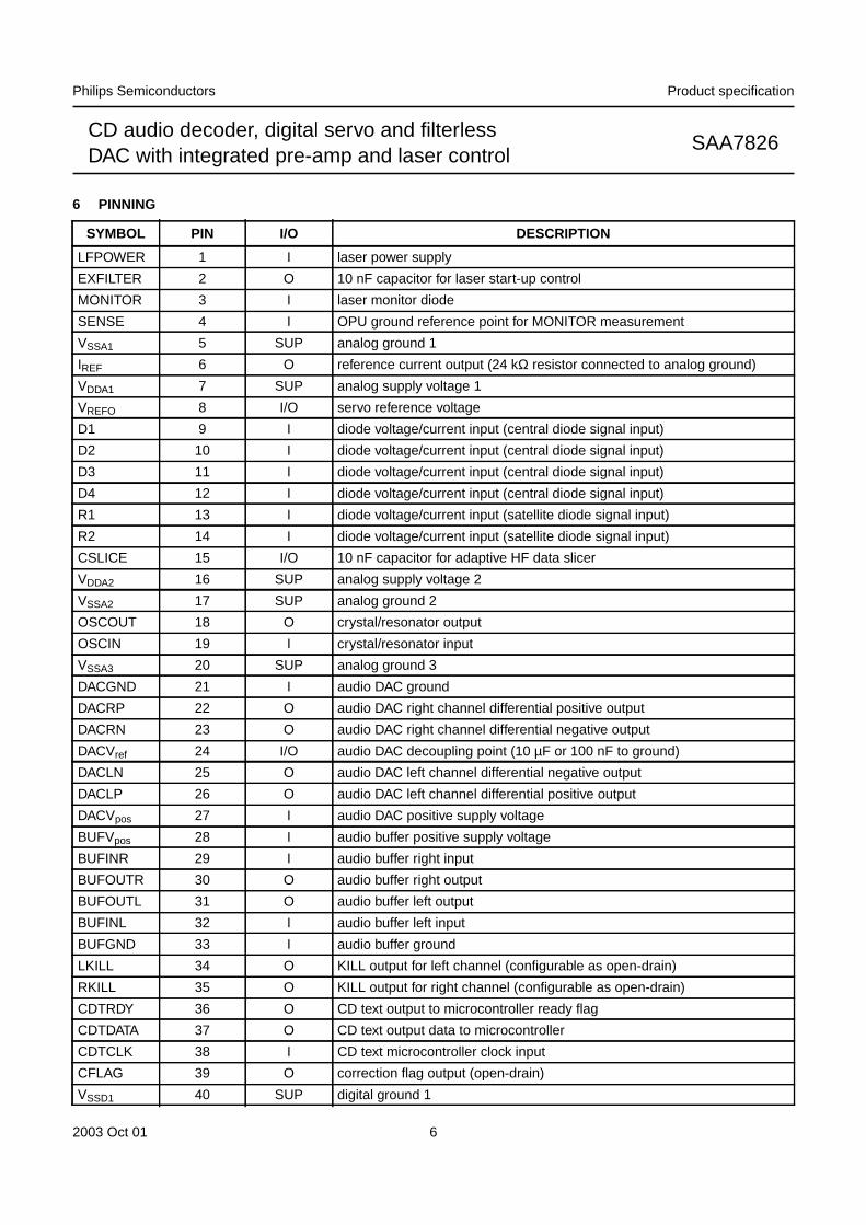
6 PINNING
SYMBOL PIN I/O DESCRIPTION
LFPOWER 1 I laser power supply
EXFILTER 2 O 10 nF capacitor for laser start-up control
MONITOR 3 I laser monitor diode
SENSE 4 I OPU ground reference point for MONITOR measurement
VSSA1 5 SUP analog ground 1
IREF 6 O reference current output (24 kΩ resistor connected to analog ground)
VDDA1 7 SUP analog supply voltage 1
VREFO 8 I/O servo reference voltage
D1 9 I diode voltage/current input (central diode signal input)
D2 10 I diode voltage/current input (central diode signal input)
D3 11 I diode voltage/current input (central diode signal input)
D4 12 I diode voltage/current input (central diode signal input)
R1 13 I diode voltage/current input (satellite diode signal input)
R2 14 I diode voltage/current input (satellite diode signal input)
CSLICE 15 I/O 10 nF capacitor for adaptive HF data slicer
VDDA2 16 SUP analog supply voltage 2
VSSA2 17 SUP analog ground 2
OSCOUT 18 O crystal/resonator output
OSCIN 19 I crystal/resonator input
VSSA3 20 SUP analog ground 3
DACGND 21 I audio DAC ground
DACRP 22 O audio DAC right channel differential positive output
DACRN 23 O audio DAC right channel differential negative output
DACVref 24 I/O audio DAC decoupling point (10 µF or 100 nF to ground)
DACLN 25 O audio DAC left channel differential negative output
DACLP 26 O audio DAC left channel differential positive output
DACVpos 27 I audio DAC positive supply voltage
BUFVpos 28 I audio buffer positive supply voltage
BUFINR 29 I audio buffer right input
BUFOUTR 30 O audio buffer right output
BUFOUTL 31 O audio buffer left output
BUFINL 32 I audio buffer left input
BUFGND 33 I audio buffer ground
LKILL 34 O KILL output for left channel (configurable as open-drain)
RKILL 35 O KILL output for right channel (configurable as open-drain)
CDTRDY 36 O CD text output to microcontroller ready flag
CDTDATA 37 O CD text output data to microcontroller
CDTCLK 38 I CD text microcontroller clock input
CFLAG 39 O correction flag output (open-drain)
VSSD1 40 SUP digital ground 1
2003 Oct 01 7
Philips Semiconductors Product specification
CD audio decoder, digital servo and filterlessDAC with integrated pre-amp and laser control
SAA7826
VDDD1 41 SUP digital supply voltage 1
SDI 42 I serial data input (loopback)
WCLI 43 I word clock input (loopback)
SCLI 44 I serial bit clock input (loopback)
EF 45 O C2 error flag output
DATA 46 O serial data output
WCLK 47 O word clock output
SCLK 48 O serial clock output
CLK16 49 O 16 MHz clock output
CLK4/12 50 O configurable 4 MHz or 12 MHz clock output
RESET 51 I power-on reset input (active LOW)
SDA 52 I/O microcontroller interface data input/output (open-drain)
SCL 53 I microcontroller interface clock input
RAB 54 I microcontroller interface R/W and load control input (4-wire)
SILD 55 I microcontroller interface R/W and load control input (4-wire)
STATUS 56 O servo interrupt request line/decoder status register/DC offset valuereadback output
RCK 57 I subcode clock input
SUB 58 O P to W subcode output
SFSY 59 O subcode frame sync output
SBSY 60 O subcode block sync output
VSSD2 61 SUP digital ground 2
DOBM 62 O bi-phase mark output (externally buffered)
VDDD2 63 SUP digital supply voltage 2
RA 64 O radial actuator output
FO 65 O focus actuator output
SL 66 O sledge actuator output
MOTO1 67 O motor output 1 output
MOTO2 68 O motor output 2 output
VSSD3 69 SUP digital ground 3
VDDD3 70 SUP digital supply voltage 3
V1 71 I versatile pin 1 input
V2 72 I versatile pin 2 input
V3 73 O versatile pin 3 output
V4 74 O versatile pin 4 output
V5 75 O versatile pin 5 output
TEST1 76 I test pin 1 input
TEST2 77 I test pin 2 input
TEST3 78 I test pin 3 input
TEST4 79 I test pin 4 input
LASER 80 O laser drive output
SYMBOL PIN I/O DESCRIPTION
2003 Oct 01 8
Philips Semiconductors Product specification
CD audio decoder, digital servo and filterlessDAC with integrated pre-amp and laser control
SAA7826
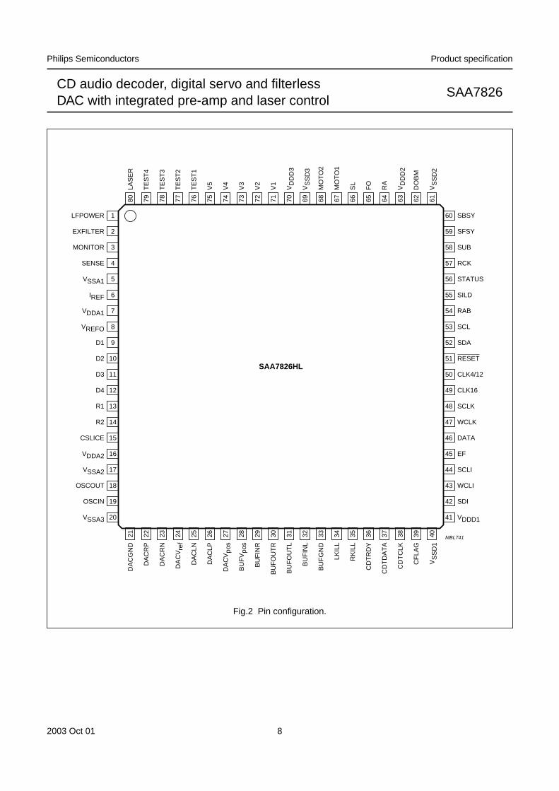
handbook, full pagewidth
SAA7826HL
MBL741
1
2
3
4
5
6
7
8
9
10
11
12
13
14
15
16
17
18
19
20
60
59
58
57
56
55
54
53
52
51
50
49
48
47
46
45
44
43
42
41
21 22 23 24 25 26 27 28 29 30 31 32 33 34 35 36 37 38 39 40
80 79 78 77 76 75 74 73 72 71 70 69 68 67 66 65 64 63 62 61
LAS
ER
TE
ST
4
TE
ST
3
TE
ST
2
TE
ST
1
V5
V4
V3
V2
V1
VD
DD
3
VS
SD
3
MO
TO
2
MO
TO
1
SL
FO
RA
VD
DD
2
DO
BM
VS
SD
2
DA
CG
ND
DA
CR
P
DA
CR
N
DA
CV
ref
DA
CLN
DA
CLP
DA
CV
pos
BU
FV
pos
BU
FIN
R
BU
FO
UT
R
BU
FO
UT
L
BU
FIN
L
BU
FG
ND
LKIL
L
RK
ILL
CD
TR
DY
CD
TD
AT
A
CD
TC
LK
CF
LAG
VS
SD
1
LFPOWER
EXFILTER
MONITOR
SENSE
VSSA1
IREF
VDDA1
VREFO
D1
D2
D3
D4
R1
R2
CSLICE
VDDA2
VSSA2
OSCOUT
OSCIN
VSSA3
SBSY
SFSY
SUB
RCK
STATUS
SILD
RAB
SCL
SDA
RESET
CLK4/12
CLK16
SCLK
WCLK
DATA
EF
SCLI
WCLI
SDI
VDDD1
Fig.2 Pin configuration.
2003 Oct 01 9
Philips Semiconductors Product specification
CD audio decoder, digital servo and filterlessDAC with integrated pre-amp and laser control
SAA7826
7 FUNCTIONAL DESCRIPTION
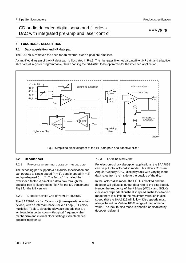
7.1 Data acquisition and HF data path
The SAA7826 removes the need for an external diode signal pre-amplifier.
A simplified diagram of the HF data path is illustrated in Fig.3. The high-pass filter, equalizing filter, HF gain and adaptiveslicer are all register programmable, thus enabling the SAA7826 to be optimized for the intended application.
handbook, full pagewidth
MBL438
op-ampcomp
67.7 MHz
THRESHOLDCONTROL
sliceddata
adaptive slicer
op-amp
op-amp
bypass
Vana
summing amplifier
equalisingfilterhigh-pass filter
Vref
d4_hf
d1_hf
hf_gain 5:0
d2_hf
d3_hf
Fig.3 Simplified block diagram of the HF data path and adaptive slicer.
7.2 Decoder part
7.2.1 PRINCIPLE OPERATING MODES OF THE DECODER
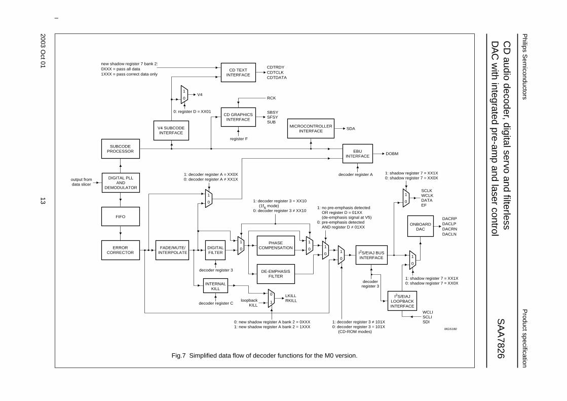
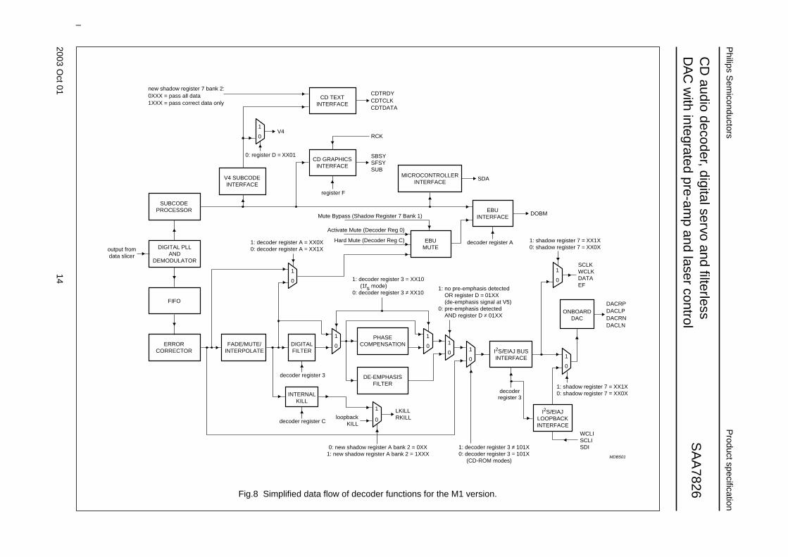
The decoding part supports a full audio specification andcan operate at single-speed (n = 1), double-speed (n = 2)and quad-speed (n = 4). The factor ‘n’ is called theoverspeed factor. A simplified data flow through thedecoder part is illustrated in Fig.7 for the M0 version andFig.8 for the M1 version.
7.2.2 DECODER SPEED AND CRYSTAL FREQUENCY
The SAA7826 is a 1×, 2× and 4× (three-speed) decodingdevice, with an internal Phase-Locked Loop (PLL) clockmultiplier. Table 1 gives the playback speeds that areachievable in conjunction with crystal frequency, themechanism and internal clock settings (selectable viadecoder register B).
7.2.3 LOCK-TO-DISC MODE
For electronic shock absorption applications, the SAA7826can be put into lock-to-disc mode. This allows ConstantAngular Velocity (CAV) disc playback with varying inputdata rates from the inside to the outside of the disc.
In the lock-to-disc mode, the FIFO is blocked and thedecoder will adjust its output data rate to the disc speed.Hence, the frequency of the I2S-bus (WCLK and SCLK)clocks are dependent on the disc speed. In the lock-to-discmode there is a limit on the maximum variation in discspeed that the SAA7826 will follow. Disc speeds mustalways be within 25% to 100% range of their nominalvalue. The lock-to-disc mode is enabled or disabled bydecoder register E.
2003 Oct 01 10
Philips Semiconductors Product specification
CD audio decoder, digital servo and filterlessDAC with integrated pre-amp and laser control
SAA7826
7.2.4 STANDBY MODES
The SAA7826 can be placed in two standby modes,selected by decoder register B (it should be noted that thedevice core is still active):
• Standby 1: CD STOP mode; most I/O functions areswitched off
• Standby 2: CD PAUSE mode; audio output features areswitched off, but the motor loop, the motor output andthe subcode interfaces remain active; this is also calleda ‘Hot Pause’.
In the standby modes the various pins will have thefollowing values:
• MOTO1 and MOTO2: put in to high-impedance, PWMmode (Standby 1 and RESET: operating in Standby 2);put in high-impedance, PDM mode (Standby 1 andRESET: operating in Standby 2)
• Pins SCL and SDA: no interaction; normal operationcontinues
• Pins SCLK, WCLK, DATA, EF and DOBM: 3-state inboth standby modes; normal operation continues afterreset
• Pins OSCIN, OSCOUT, CLK16 and CLK4/12: nointeraction; normal operation continues
• Pins V1 to V5 and CFLAG: no interaction; normaloperation continues.
Table 1 Playback speeds
7.3 Crystal oscillator
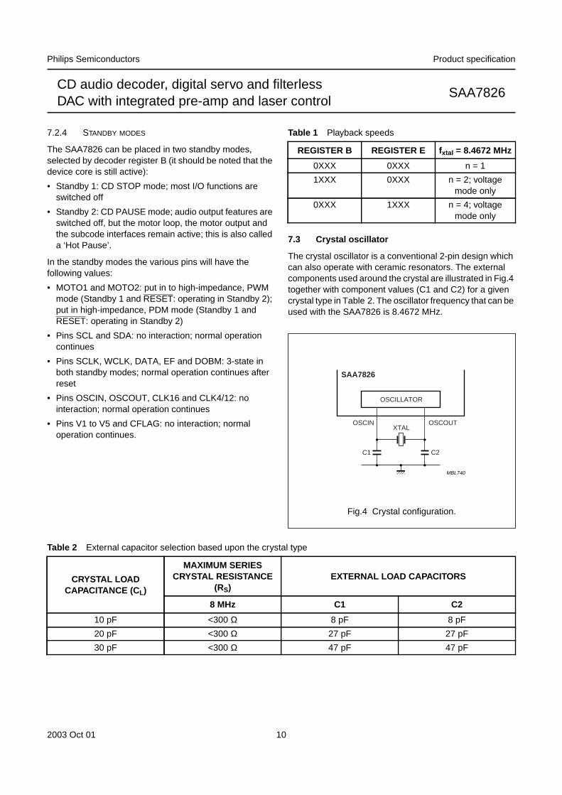
The crystal oscillator is a conventional 2-pin design whichcan also operate with ceramic resonators. The externalcomponents used around the crystal are illustrated in Fig.4together with component values (C1 and C2) for a givencrystal type in Table 2. The oscillator frequency that can beused with the SAA7826 is 8.4672 MHz.
REGISTER B REGISTER E fxtal = 8.4672 MHz
0XXX 0XXX n = 1
1XXX 0XXX n = 2; voltagemode only
0XXX 1XXX n = 4; voltagemode only
handbook, halfpage SAA7826
OSCILLATOR
XTALOSCOUTOSCIN
C2C1
MBL740
Fig.4 Crystal configuration.
Table 2 External capacitor selection based upon the crystal type
CRYSTAL LOADCAPACITANCE (C L)
MAXIMUM SERIESCRYSTAL RESISTANCE
(RS)EXTERNAL LOAD CAPACITORS
8 MHz C1 C2
10 pF <300 Ω 8 pF 8 pF
20 pF <300 Ω 27 pF 27 pF
30 pF <300 Ω 47 pF 47 pF
2003 Oct 01 11
Philips Semiconductors Product specification
CD audio decoder, digital servo and filterlessDAC with integrated pre-amp and laser control
SAA7826
7.4 Data slicer and bit clock regenerator
The SAA7826 has an integrated adaptive data slicer whichis clocked at 67 MHz. The slice level is controlled byinternal current sources which are switched onto andintegrated by the external capacitor connected to theCSLICE pin. The currents are switched under the controlof a Digital Phase-Locked loop (DPLL).
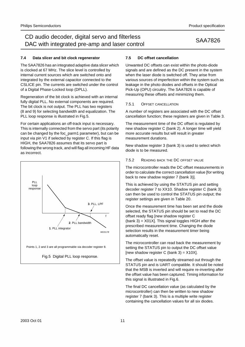
Regeneration of the bit clock is achieved with an internalfully digital PLL. No external components are required.The bit clock is not output. The PLL has two registers(8 and 9) for selecting bandwidth and equalization. ThePLL loop response is illustrated in Fig.5.
For certain applications an off-track input is necessary.This is internally connected from the servo part (its polaritycan be changed by the foc_parm1 parameter), but can beinput via pin V1 if selected by register C. If this flag isHIGH, the SAA7826 assumes that its servo part isfollowing the wrong track, and will flag all incoming HF dataas incorrect.
7.5 DC offset cancellation
Unwanted DC offsets can exist within the photo-diodesignals and are defined as the DC present in the systemwhen the laser diode is switched off. They arise fromvarious sources of imperfection within the system such asleakage in the photo diodes and offsets in the OpticalPick-Up (OPU) circuitry. The SAA7826 is capable ofmeasuring these offsets and minimizing them.
7.5.1 OFFSET CANCELLATION
A number of registers are associated with the DC offsetcancellation function; these registers are given in Table 3.
The measurement time of the DC offset is regulated bynew shadow register C (bank 2). A longer time will yieldmore accurate results but will result in greatermeasurement durations.
New shadow register 3 (bank 3) is used to select whichdiode is to be measured.
7.5.2 READING BACK THE DC OFFSET VALUE
The microcontroller reads the DC offset measurements inorder to calculate the correct cancellation value [for writingback to new shadow register 7 (bank 3)].
This is achieved by using the STATUS pin and settingdecoder register 7 to XX10. Shadow register C (bank 3)can then be used to control the STATUS pin output; theregister settings are given in Table 20.
Once the measurement time has been set and the diodeselected, the STATUS pin should be set to read the DCoffset ready flag [new shadow register C(bank 3) = X01X]. This signal toggles HIGH after theprescribed measurement time. Changing the diodeselection results in the measurement timer beingautomatically reset.
The microcontroller can read back the measurement bysetting the STATUS pin to output the DC offset value[new shadow register C (bank 3) = X10X].
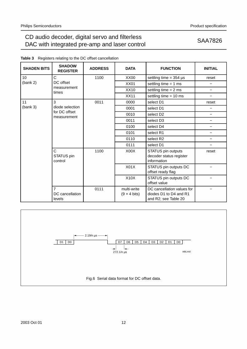
The offset value is repeatedly streamed out through theSTATUS pin and is UART compatible. It should be notedthat the MSB is inverted and will require re-inverting afterthe offset value has been captured. Timing information forthis signal is illustrated in Fig.6.
The final DC cancellation value (as calculated by themicrocontroller) can then be written to new shadowregister 7 (bank 3). This is a multiple write registercontaining the cancellation values for all six diodes.
MGS178
handbook, halfpage
f
3. PLL, LPF
2. PLL bandwidth
1. PLL integrator
PLLloop
response
Fig.5 Digital PLL loop response.
Points 1, 2 and 3 are all programmable via decoder register 8.
2003 Oct 01 12
Philips Semiconductors Product specification
CD audio decoder, digital servo and filterlessDAC with integrated pre-amp and laser control
SAA7826
Table 3 Registers relating to the DC offset cancellation
SHADEN BITSSHADOW
REGISTERADDRESS DATA FUNCTION INITIAL
10(bank 2)
CDC offsetmeasurementtimes
1100 XX00 settling time = 354 µs reset
XX01 settling time = 1 ms −XX10 settling time = 2 ms −XX11 settling time = 10 ms −
11(bank 3)
3diode selectionfor DC offsetmeasurement
0011 0000 select D1 reset
0001 select D1 −0010 select D2 −0011 select D3 −0100 select D4 −0101 select R1 −0110 select R2 −0111 select D1 −
CSTATUS pincontrol
1100 X00X STATUS pin outputsdecoder status registerinformation
reset
X01X STATUS pin outputs DCoffset ready flag
−
X10X STATUS pin outputs DCoffset value
−
7DC cancellationlevels
0111 multi-write(9 × 4 bits)
DC cancellation values fordiodes D1 to D4 and R1and R2; see Table 20
−
handbook, full pagewidth
MBL440
D7 D6 D5 D4 D3 D2 D1 D0D0D1
272.1/n µs
2.19/n µs
Fig.6 Serial data format for DC offset data.
2003O
ct0113
Philips S
emiconductors
Product specification
CD
audio decoder, digital servo and filterlessD
AC
with integrated pre-am
p and laser controlS
AA
7826
This text is here in white to force landscape pages to be rotated correctly when browsing through the pdf in the Acrobat reader.This text is here in_white to force landscape pages to be rotated correctly when browsing through the pdf in the Acrobat reader.This text is here inThis text is here inwhite to force landscape pages to be rotated correctly when browsing through the pdf in the Acrobat reader. white to force landscape pages to be ...
handbook, full pagewidth
SUBCODEPROCESSOR
DIGITAL PLLAND
DEMODULATOR
FIFO
ERRORCORRECTOR
FADE/MUTE/INTERPOLATE
DIGITALFILTER
PHASECOMPENSATION
DE-EMPHASISFILTER
INTERNALKILL
1
01
0
1
0
1
0
1
0I2S/EIAJ BUSINTERFACE
I2S/EIAJLOOPBACKINTERFACE
WCLISCLISDI
DACRPDACLPDACRNDACLN
SCLKWCLKDATAEF
decoderregister 3
decoder register C
decoder register 3
register F
decoder register A
1
0
1
0
1: decoder register 3 ≠ 101X0: decoder register 3 = 101X (CD-ROM modes)
0: new shadow register A bank 2 = 0XXX1: new shadow register A bank 2 = 1XXX
1: shadow register 7 = XX1X0: shadow register 7 = XX0X
1: shadow register 7 = XX1X0: shadow register 7 = XX0X
0: register D = XX01
1: decoder register A = XX0X0: decoder register A ≠ XX1X
V4 SUBCODEINTERFACE
MICROCONTROLLERINTERFACE
CD GRAPHICSINTERFACE
CD TEXTINTERFACE
EBUINTERFACE
SBSYSFSYSUB
RCK
DOBM
V4
SDA
output fromdata slicer
1: decoder register 3 = XX10 (1fs mode)0: decoder register 3 ≠ XX10
1: no pre-emphasis detected OR register D = 01XX (de-emphasis signal at V5)0: pre-emphasis detected AND register D ≠ 01XX
LKILLRKILLloopback
KILL
MGS180
1
0
ONBOARDDAC
CDTRDYCDTCLKCDTDATA
new shadow register 7 bank 2:0XXX = pass all data1XXX = pass correct data only
1
0
Fig.7 Simplified data flow of decoder functions for the M0 version.
2003O
ct0114
Philips S
emiconductors
Product specification
CD
audio decoder, digital servo and filterlessD
AC
with integrated pre-am
p and laser controlS
AA
7826
This text is here in white to force landscape pages to be rotated correctly when browsing through the pdf in the Acrobat reader.This text is here in_white to force landscape pages to be rotated correctly when browsing through the pdf in the Acrobat reader.This text is here inThis text is here inwhite to force landscape pages to be rotated correctly when browsing through the pdf in the Acrobat reader. white to force landscape pages to be ...
handbook, full pagewidth
SUBCODEPROCESSOR
DIGITAL PLLAND
DEMODULATOR
FIFO
ERRORCORRECTOR
FADE/MUTE/INTERPOLATE
DIGITALFILTER
PHASECOMPENSATION
DE-EMPHASISFILTER
INTERNALKILL
1
01
0
1
0
1
0
1
0I2S/EIAJ BUSINTERFACE
I2S/EIAJLOOPBACKINTERFACE
WCLISCLISDI
DACRPDACLPDACRNDACLN
SCLKWCLKDATAEF
decoderregister 3
decoder register C
decoder register 3
register F
decoder register A
1
0
0
1
1: decoder register 3 ≠ 101X0: decoder register 3 = 101X (CD-ROM modes)
0: new shadow register A bank 2 = 0XX1: new shadow register A bank 2 = 1XXX
1: shadow register 7 = XX1X0: shadow register 7 = XX0X
1: shadow register 7 = XX1X0: shadow register 7 = XX0X
0: register D = XX01
1: decoder register A = XX0X0: decoder register A = XX1X
Activate Mute (Decoder Reg 0)
Mute Bypass (Shadow Register 7 Bank 1)
Hard Mute (Decoder Reg C)
V4 SUBCODEINTERFACE
MICROCONTROLLERINTERFACE
CD GRAPHICSINTERFACE
CD TEXTINTERFACE
EBUINTERFACE
EBUMUTE
SBSYSFSYSUB
RCK
DOBM
V4
SDA
output fromdata slicer
1: decoder register 3 = XX10 (1fs mode)0: decoder register 3 ≠ XX10
1: no pre-emphasis detected OR register D = 01XX (de-emphasis signal at V5)0: pre-emphasis detected AND register D ≠ 01XX
LKILLRKILLloopback
KILL
MDB501
1
0
ONBOARDDAC
CDTRDYCDTCLKCDTDATA
new shadow register 7 bank 2:0XXX = pass all data1XXX = pass correct data only
1
0
Fig.8 Simplified data flow of decoder functions for the M1 version.
2003 Oct 01 15
Philips Semiconductors Product specification
CD audio decoder, digital servo and filterlessDAC with integrated pre-amp and laser control
SAA7826
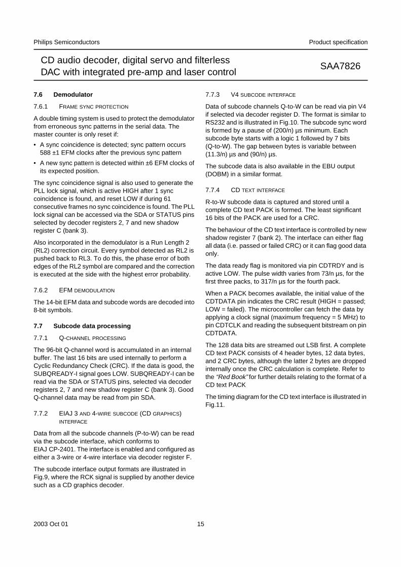
7.6 Demodulator
7.6.1 FRAME SYNC PROTECTION
A double timing system is used to protect the demodulatorfrom erroneous sync patterns in the serial data. Themaster counter is only reset if:
• A sync coincidence is detected; sync pattern occurs588 ±1 EFM clocks after the previous sync pattern
• A new sync pattern is detected within ±6 EFM clocks ofits expected position.
The sync coincidence signal is also used to generate thePLL lock signal, which is active HIGH after 1 synccoincidence is found, and reset LOW if during 61consecutive frames no sync coincidence is found. The PLLlock signal can be accessed via the SDA or STATUS pinsselected by decoder registers 2, 7 and new shadowregister C (bank 3).
Also incorporated in the demodulator is a Run Length 2(RL2) correction circuit. Every symbol detected as RL2 ispushed back to RL3. To do this, the phase error of bothedges of the RL2 symbol are compared and the correctionis executed at the side with the highest error probability.
7.6.2 EFM DEMODULATION
The 14-bit EFM data and subcode words are decoded into8-bit symbols.
7.7 Subcode data processing
7.7.1 Q-CHANNEL PROCESSING
The 96-bit Q-channel word is accumulated in an internalbuffer. The last 16 bits are used internally to perform aCyclic Redundancy Check (CRC). If the data is good, theSUBQREADY-I signal goes LOW. SUBQREADY-I can beread via the SDA or STATUS pins, selected via decoderregisters 2, 7 and new shadow register C (bank 3). GoodQ-channel data may be read from pin SDA.
7.7.2 EIAJ 3 AND 4-WIRE SUBCODE (CD GRAPHICS)INTERFACE
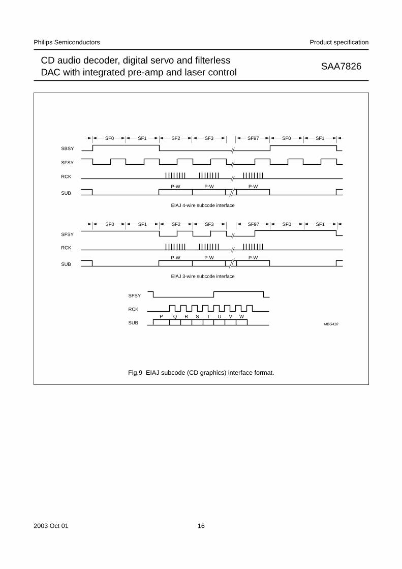
Data from all the subcode channels (P-to-W) can be readvia the subcode interface, which conforms toEIAJ CP-2401. The interface is enabled and configured aseither a 3-wire or 4-wire interface via decoder register F.
The subcode interface output formats are illustrated inFig.9, where the RCK signal is supplied by another devicesuch as a CD graphics decoder.
7.7.3 V4 SUBCODE INTERFACE
Data of subcode channels Q-to-W can be read via pin V4if selected via decoder register D. The format is similar toRS232 and is illustrated in Fig.10. The subcode sync wordis formed by a pause of (200/n) µs minimum. Eachsubcode byte starts with a logic 1 followed by 7 bits(Q-to-W). The gap between bytes is variable between(11.3/n) µs and (90/n) µs.
The subcode data is also available in the EBU output(DOBM) in a similar format.
7.7.4 CD TEXT INTERFACE
R-to-W subcode data is captured and stored until acomplete CD text PACK is formed. The least significant16 bits of the PACK are used for a CRC.
The behaviour of the CD text interface is controlled by newshadow register 7 (bank 2). The interface can either flagall data (i.e. passed or failed CRC) or it can flag good dataonly.
The data ready flag is monitored via pin CDTRDY and isactive LOW. The pulse width varies from 73/n µs, for thefirst three packs, to 317/n µs for the fourth pack.
When a PACK becomes available, the initial value of theCDTDATA pin indicates the CRC result (HIGH = passed;LOW = failed). The microcontroller can fetch the data byapplying a clock signal (maximum frequency = 5 MHz) topin CDTCLK and reading the subsequent bitstream on pinCDTDATA.
The 128 data bits are streamed out LSB first. A completeCD text PACK consists of 4 header bytes, 12 data bytes,and 2 CRC bytes, although the latter 2 bytes are droppedinternally once the CRC calculation is complete. Refer tothe “Red Book” for further details relating to the format of aCD text PACK
The timing diagram for the CD text interface is illustrated inFig.11.
2003 Oct 01 16
Philips Semiconductors Product specification
CD audio decoder, digital servo and filterlessDAC with integrated pre-amp and laser control
SAA7826
handbook, full pagewidth
SBSY
SFSY
RCK
SUB
SFSY
RCK
SUB
SFSY
RCK
SUB
EIAJ 4-wire subcode interface
EIAJ 3-wire subcode interface
SF0 SF1 SF2 SF3 SF97 SF0 SF1
P-W P-W P-W
P-W P-W P-W
P Q R S T U V W
MBG410
SF0 SF1 SF2 SF3 SF97 SF0 SF1
Fig.9 EIAJ subcode (CD graphics) interface format.
2003 Oct 01 17
Philips Semiconductors Product specification
CD audio decoder, digital servo and filterlessDAC with integrated pre-amp and laser control
SAA7826
W96 1 Q R S T U V W 1 Q
200/n µsmin
11.3/nµs
11.3/n µs min90/n µs max
MBG401
Fig.10 Subcode format and timing on pin V4.
Where n = disc speed.
handbook, full pagewidth
CRC flag D0 D1 D2 D3 D126 D127
CDTCLK
CDTRDY
CDTDATA
MBL441
73/n µs to 317/n µs
~1/n ns200 ns (min)
Fig.11 CD text interface format and timing.
Where n = disc speed.
7.8 FIFO and error correction
The SAA7826 has a ±8 frame FIFO. The error corrector isa t = 2, e = 4 type, with error corrections on both C1(32 symbol) and C2 (28 symbol) frames. Four symbols areused from each frame as parity symbols. This errorcorrector can correct up to two errors on the C1 level andup to four errors on the C2 level.
The error corrector also contains a flag processor. Flagsare assigned to symbols when the error corrector cannotascertain if the symbols are definitely good. C1 generatesoutput flags which are read after de-interleaving by C2, tohelp in the generation of C2 output flags.
The C2 output flags are used by the interpolator forconcealment of uncorrectable errors. They are also outputvia the EBU signal (DOBM). The EF output flags bytes inerror in both audio and CD-ROM modes.
7.8.1 FLAGS OUTPUT (CFLG)
The flags output pin CFLG shows the status of the errorcorrector and interpolator and is updated every frame(7.35 × n kHz). In the SAA7826, 8 × 1-bit flags are presenton the CFLG pin as illustrated in Fig.12. This signal showsthe status of the error corrector and interpolator.
The first flag bit, F1, is the absolute time sync signal, theFIFO-passed subcode sync and relates the position of thesubcode sync to the audio data (DAC output). This flagmay also be used in a super FIFO or in the synchronizationof different players. The output flags can be madeavailable at bit 4 of the EBU data format (LSB of the 24-bitdata word), if selected by decoder register A.
2003 Oct 01 18
Philips Semiconductors Product specification
CD audio decoder, digital servo and filterlessDAC with integrated pre-amp and laser control
SAA7826
handbook, full pagewidth
F1 F2 F3 F4 F5 F6 F7 F8 F1F8
11.3/nµs 33.9/n µs33.9/n µs
MBG425
Fig.12 Flag output timing diagram.
Where n = disc speed.
Table 4 Output flags
F1 F2 F3 F4 F5 F6 F7 F8 DESCRIPTION
0 X X X X X X X no absolute time sync
1 X X X X X X X absolute time sync
X 0 0 X X X X X C1 frame contained no errors
X 0 1 X X X X X C1 frame contained 1 error
X 1 0 X X X X X C1 frame contained 2 errors
X 1 1 X X X X X C1 frame uncorrectable
X X X 0 0 X X 0 C2 frame contained no errors
X X X 0 0 X X 1 C2 frame contained 1 error
X X X 0 1 X X 0 C2 frame contained 2 errors
X X X 0 1 X X 1 C2 frame contained 3 errors
X X X 1 0 X X 0 C2 frame contained 4 errors
X X X 1 1 X X 1 C2 frame uncorrectable
X X X X X 0 0 X no interpolations
X X X X X 0 1 X at least one 1-sample interpolation
X X X X X 1 0 X at least one hold and no interpolations
X X X X X 1 1 X at least one hold and one 1-sample interpolation
2003 Oct 01 19
Philips Semiconductors Product specification
CD audio decoder, digital servo and filterlessDAC with integrated pre-amp and laser control
SAA7826
7.9 Audio functions
7.9.1 DE-EMPHASIS AND PHASE LINEARITY
When pre-emphasis is detected in the Q-channelsubcode, the digital filter automatically includes ade-emphasis filter section. When de-emphasis is notrequired, a phase compensation filter section will controlthe phase of the digital oversampling filter to ≤ ±1° withinthe 0 to 16 kHz band. With de-emphasis the filter is notphase linear.
If the de-emphasis signal is set to be available at pin V5,selected via decoder register D, then the de-emphasisfilter is bypassed.
7.9.2 DIGITAL OVERSAMPLING FILTER
For optimization of performance with an external DAC, theSAA7826 contains a 2 to 4 times oversampling IIR filter.The filter specification of the 4 times oversampling filter isgiven in Table 5.
The attenuation does not include the sample-and-hold atthe external DAC output or the DAC post filter. When usingthe oversampling filter, the output level is scaled −0.5 dBdown to avoid overflow on full-scale sine wave inputs(0 to 20 kHz).
Table 5 Filter specification
7.9.3 CONCEALMENT
A 1-sample linear interpolator becomes active if a singlesample is flagged as erroneous but cannot be corrected.The erroneous sample is replaced by a level midwaybetween the preceding and following samples. Left andright channels have independent interpolators. If morethan one consecutive non-correctable sample is found, thelast good sample is held. A 1-sample linear interpolation isthen performed before the next good sample; see Fig.13.
In CD-ROM modes (i.e. the external DAC interface isselected to be in a CD-ROM format) concealment is notexecuted.
7.9.4 MUTE, FULL-SCALE, ATTENUATION AND FADE
A digital level controller is present on the SAA7826 whichperforms the functions of soft mute, full-scale, attenuationand fade; these are selected via decoder register 0:
• Mute: signal reduced to 0 in a maximum of 128 steps;3/n ms
• Attenuation: signal scaled by −12 dB
• Full-scale: ramp signal back to 0 dB level; from mute ittakes 3/n ms
• Fade: activates a 128 stage counter which allows thesignal to be scaled up or down in 0.07 dB steps
– 128 = full-scale
– 120 = −0.5 dB (i.e. full-scale if oversampling filter isused)
– 32 = −12 dB
– 0 = mute.
7.9.5 PEAK DETECTOR
The peak detector measures the highest audio level(absolute value) on positive peaks for left and rightchannels. The 8 most significant bits are output in theQ-channel data in place of the CRC bits. Bits 81 to 88contain the left peak value (bit 88 = MSB) and bits 89 to 96contain the right peak value (bit 96 = MSB). The valuesare reset after reading Q-channel data via pin SDA.
PASS BAND STOP BAND ATTENUATION
0 to 9 kHz − ≤0.001 dB
19 to 20 kHz − ≤0.03 dB
− 24 kHz ≥25 dB
− 24 to 27 kHz ≥38 dB
− 27 to 35 kHz ≥40 dB
− 35 to 64 kHz ≥50 dB
− 64 to 68 kHz ≥31 dB
− 68 kHz ≥35 dB
− 69 to 88 kHz ≥40 dB
2003 Oct 01 20
Philips Semiconductors Product specification
CD audio decoder, digital servo and filterlessDAC with integrated pre-amp and laser control
SAA7826
Interpolation Hold Interpolation
MGA372
OK Error OK Error Error Error OK OK
Fig.13 Concealment mechanism.
7.10 Audio DAC interface
7.10.1 INTERNAL DYNAMIC ELEMENT MATCHING DIGITAL-TO-ANALOG CONVERTER
The onboard audio DEM DAC operates at an oversampling rate of 96fs and is designed for operation with an audio inputat 1fs. The DAC is equipped with two pairs of stereo outputs for driving medium impedance line outputs and for directlydriving low impedance headphones. A pair of analog inputs are provided to enable external audio sources to make useof the headphone output buffers.
Audio data from the decoder part of the SAA7826 can be routed as described in Sections 7.10.1.1 and 7.10.1.2.
Table 6 Shadow register
SHADEN BITSSHADOW
REGISTERADDRESS DATA FUNCTION RESET
01(bank 1)
7control ofonboard DAC
0111 0000 use external DAC or route audio databack into onboard DAC (loopbackmode)
reset
0010 route audio data directly into onboardDAC (non-loopback mode)
−
2003 Oct 01 21
Philips Semiconductors Product specification
CD audio decoder, digital servo and filterlessDAC with integrated pre-amp and laser control
SAA7826
7.10.1.1 Use of internal DAC
Setting shadow register 7 to 0010 routes audio data fromthe decoder into the internal DAC. To enable the on-boardDAC, the DAC interface format (set by register 3) must beset to 16-bit 1fs mode, either I2S-bus or EIAJ format.CD-ROM mode can also be used if interpolation is notrequired. The serial data output pins for interfacing with anexternal DAC (SCLK, WCLK, DATA and EF) are set tohigh-impedance.
7.10.1.2 Loopback external data into onboard DAC
The onboard DAC can also be set to accept serial datainputs from an external source, e.g. an Electronic ShockAbsorption (ESA) IC. This is known as loopback mode andis enabled by setting shadow register 7 to 0000. Thisenables the serial data output pins (SCLK, WCLK, DATAand EF) so that data can be routed from the SAA7826 toan external ESA system (or external DAC).
The serial data from an external ESA IC can then also beinput to the onboard DAC on the SAA7826 by utilising theserial data input interface (SCLI, SDI and WCLI).
In this mode, a wide range of data formats to the externalESA IC can be programmed as shown in Table 7.
However, the serial input on the SAA7826 always expectsthe input data from the ESA IC to be 16-bit 1fs and thesame data format, either I2S-bus or EIAJ, as the serialoutput format (set by decoder register 3).
7.10.2 EXTERNAL DAC INTERFACE
Audio data from the SAA7826 can be sent to an externalDAC, identical to the SAA732x series, in ‘loopback’ mode(i.e. shadow register 7 is set to 0000).
The SAA7826 is compatible with a wide range of externalDACs. Eleven formats are supported which are given inTable 7. Figures 14 and 15 show the Philips I2S-bus andthe EIAJ data formats respectively. When the decoder isoperated in lock-to-disc mode, the SCLK frequencydepends on the disc speed factor ‘d’.
All formats are MSB first and 1fs is 44.1 kHz. The polarityof the WCLK and the data can be inverted; selectable bydecoder register 7. It should be noted that EF is only adefined output in CD-ROM and 1fs modes.
When using an external DAC (or when using the onboardDAC in non-loopback mode), the serial data inputs to theonboard DAC (SCLI, SDI and WCLI) should be tied toground.
Table 7 DAC interface formats
Note
1. In this mode the first 16 bits contain data, but if any of the fade, attenuate or de-emphasis filter functions are activatedthen the first 18 bits contain data.
REGISTER 3SAMPLE
FREQUENCYNUMBER OF
BITSSCLK (MHz) FORMAT INTERPOLATION
1010 fs 16 2.1168 × n CD-ROM(I2S-bus)
no
1011 fs 16 2.1168 × n CD-ROM (EIAJ) no
1110 fs 16/18(1) 2.1168 × n Philips I2S-bus16/18 bits(1)
yes
0010 fs 16 2.1168 × n EIAJ 16 bits yes
0110 fs 18 2.1168 × n EIAJ 18 bits yes
0000 4fs 16 8.4672 × n EIAJ 16 bits yes
0100 4fs 18 8.4672 × n EIAJ 18 bits yes
1100 4fs 18 8.4672 × n Philips I2S-bus18 bits
yes
0011 2fs 16 4.2336 × n EIAJ 16 bits yes
0111 2fs 18 4.2336 × n EIAJ 18 bits yes
1111 2fs 18 4.2336 × n Philips I2S-bus18 bits
yes
2003O
ct0122
Philips S
emiconductors
Product specification
CD
audio decoder, digital servo and filterlessD
AC
with integrated pre-am
p and laser controlS
AA
7826
This text is here in white to force landscape pages to be rotated correctly when browsing through the pdf in the Acrobat reader.This text is here in_white to force landscape pages to be rotated correctly when browsing through the pdf in the Acrobat reader.This text is here inThis text is here inwhite to force landscape pages to be rotated correctly when browsing through the pdf in the Acrobat reader. white to force landscape pages to be ...
LEFT CHANNEL DATA (WCLK NORMAL POLARITY)
SCLK
15 14 15 141 0DATA
WCLK
LSB error flag MSB error flag LSB error flag MSB error flag EF(CD-ROMAND 1fs MODES ONLY)
01
MBG424
Fig.14 Philips I2S-bus data format (16-bit word length).
SCLK
17 170DATA
WCLK
0
LEFT CHANNEL DATA
MSB error flag LSB error flag MSB error flag
MBG423
EF(CD-ROMAND 1fs MODES ONLY)
Fig.15 EIAJ data format (18-bit word length).
2003 Oct 01 23
Philips Semiconductors Product specification
CD audio decoder, digital servo and filterlessDAC with integrated pre-amp and laser control
SAA7826
7.11 EBU interface
The bi-phase mark digital output signal at pin DOBM is inaccordance with the format defined by the IEC 60958specification. Three different modes can be selected viadecoder register A:
• DOBM pin held LOW
• Data taken before concealment, mute and fade (mustalways be used for CD-ROM modes)
• Data taken after concealment, mute and fade.
An additional mute function is available via registersShadow 7 (bank 1) and decoder register 0 and C. Theyprovide the following:
• Hard mute: immediate mute of the audio sample in ROMmode at 1×, 2× or 4× speed
• Soft mute: 3 ms ramp up or ramp down of the audiosamples in 1× audio mode
• Bypass: switches the EBU mute function out of the EBUsignal path.
7.11.1 FORMAT
The digital audio output consists of 32-bit words(‘subframes’) transmitted in bi-phase mark code (twotransitions for a logic 1 and one transition for a logic 0).Words are transmitted in blocks of 384. The EBU frameformat is given in Table 8.
Table 8 EBU frame format; see also Table 9
Table 9 Description of EBU frame function
FUNCTION BITS DESCRIPTION
Sync 0 to 3 −Auxiliary 4 to 7 not used; normally zero
Error flags 4 CFLG error and interpolation flags when selected by register A
Audio sample 8 to 27 first 4 bits not used (always zero); twos complement; LSB = bit 12, MSB = bit 27
Validity flag 28 valid = logic 0
User data 29 used for subcode data (Q-to-W)
Channel status 30 control bits and category code
Parity bit 31 even parity for bits 4 to 30
FUNCTION DESCRIPTION
Sync The sync word is formed by violation of the bi-phase rule and therefore does not contain any data.Its length is equivalent to 4 data bits. The 3 different sync patterns indicate the following situations:sync B; start of a block (384 words), word contains left sample; sync M; word contains left sample(no block start) and sync W; word contains right sample.
Audio sample Left and right samples are transmitted alternately.
Validity flag Audio samples are flagged (bit 28 = 1) if an error has been detected but was uncorrectable. Thisflag remains the same even if data is taken after concealment.
User data Subcode bits Q-to-W from the subcode section are transmitted via the user data bit. This data isasynchronous with the block rate.
Channel status The channel status bit is the same for left and right words. Therefore a block of 384 words contains192 channel status bits. The category code is always CD. The bit assignment is given in Table 10.
2003 Oct 01 24
Philips Semiconductors Product specification
CD audio decoder, digital servo and filterlessDAC with integrated pre-amp and laser control
SAA7826
Table 10 Bit assignment
FUNCTION BITS DESCRIPTION
Control 0 to 3 copy of CRC checked Q-channel control bits 0 to 3; bit 2 is logic 1 when copypermitted; bit 3 is logic 1 when recording has pre-emphasis
Reserved mode 4 to 7 always zero
Category code 8 to 15 CD: bit 8 = logic 1, all other bits = logic 0
Clock accuracy 28 to 29 set by register A; 10 = level I; 00 = level II; 01 = level III
Remaining 6 to 27 and30 to 191
always zero
7.12 KILL features
7.12.1 THE KILL CIRCUIT
The KILL circuit detects digital silence by testing for anall-zero or all-ones data word in the left and right channels.This occurs in two places; prior to the digital filter (internalKILL), and in the digital DAC (loopback/external KILL).Programming bit 3 of new shadow register A (bank 2)determines whether internal or external data is used. Theoutput is switched to active HIGH when silence has beendetected for at least 270 ms, or if mute is active, or inCD-ROM mode. Two KILL modes are available which canbe selected by decoder register C:
• Mono KILL: LKILL and RKILL are both active HIGHwhen silence is detected on left and right channelssimultaneously
• Stereo KILL: LKILL and RKILL are active HIGHindependently of each other when silence is detected oneither channel.
7.12.2 SILENCE INJECTION
The silence inject function monitors the left and right KILLsignals and forces the analog DAC into silence when KILLis asserted. This improves the internal Signal-to-NoiseRatio (S/N) by preventing any spurious noise fromreaching the DAC. The silence inject function can beenabled or disabled by programming bit 2 of the newshadow register A (bank 2).
7.13 Audio features off
The audio features can be turned off (selected by decoderregister E) and will affect the following functions:
• Digital filter, fade, peak detector, internal KILL circuit(although RKILL and LKILL outputs are still active) aredisabled
• V5 (if selected to be the de-emphasis flag output) andthe EBU outputs become undefined.
The EBU output should be set LOW prior to switching theaudio features off and after switching the audio featuresback on; a full-scale command should be given.
7.14 The versatile pins interface
The SAA7826 has five pins that can be reconfigured fordifferent applications.
The functions of these versatile pins are identical to theSAA732x series and can be programmed by decoderregisters C, D and shadow register 3 (bank 1) as shown inTable 11.
2003 Oct 01 25
Philips Semiconductors Product specification
CD audio decoder, digital servo and filterlessDAC with integrated pre-amp and laser control
SAA7826
Table 11 Pin applications
PINNAME
PINNUMBER
TYPEREGISTERADDRESS
REGISTERDATA
FUNCTION
V1 71 input 1100 XXX1 external off-track signal input
− XXX0 internal off-track signal used input may be readvia decoder status bit; selected via register 2
V2 72 input − − input may be read via decoder status bit;selected via register 2
V3 73 output 1100 00XX output = 0
− 01XX output = 1
V4 74 output 1101 0000 4-line motor drive (using V4 and V5)
− XX01 Q-to-W subcode output
− XX10 output = 0
− XX11 output = 1
V5 75 output 1101 01XX de-emphasis output (active HIGH)
− 10XX output = 0
− 11XX output = 1
7.15 Spindle motor control
7.15.1 MOTOR OUTPUT MODES
The spindle motor speed is controlled by a fully integrateddigital servo. Address information from the internal±8 frame FIFO and disc speed information are used tocalculate the motor control output signals. Several outputmodes, selected by decoder register 6, are supported:
• Pulse density, 2-line (true complement output),(1 × n) MHz sample frequency
• PWM output, 2-line, (22.05 × n) kHz modulationfrequency
• PWM output, 4-line, (22.05 × n) kHz modulationfrequency
• CDV motor mode.
7.15.1.1 Pulse density output mode
In the pulse density mode the motor output pin (MOTO1)is the pulse density modulated motor output signal.
A 50% duty factor corresponds with the motor notactuated, higher duty factors mean acceleration, lowerduty factors means braking. In this mode, the MOTO2signal is the inverse of the MOTO1 signal. Both signalschange state only on the edges of a (1 × n) MHz internalclock signal.
7.15.1.2 PWM output mode (2-line)
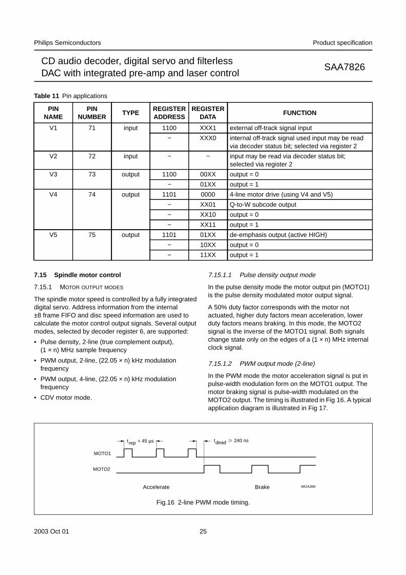
In the PWM mode the motor acceleration signal is put inpulse-width modulation form on the MOTO1 output. Themotor braking signal is pulse-width modulated on theMOTO2 output. The timing is illustrated in Fig 16. A typicalapplication diagram is illustrated in Fig 17.
rept = 45 µs t 240 nsdead
Accelerate Brake
MOTO1
MOTO2
MGA366
Fig.16 2-line PWM mode timing.
2003 Oct 01 26
Philips Semiconductors Product specification
CD audio decoder, digital servo and filterlessDAC with integrated pre-amp and laser control
SAA7826
MGA365 - 2VSS
+
M
MOTO1 MOTO2
10 Ω 100 nF
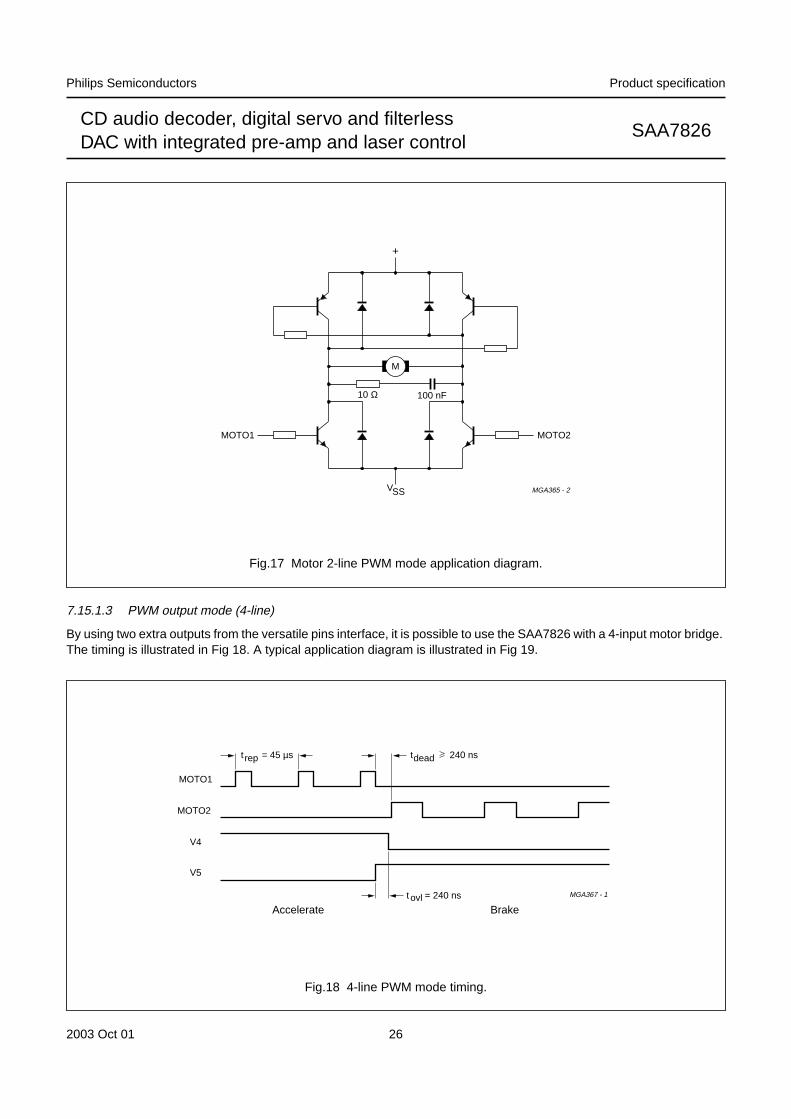
Fig.17 Motor 2-line PWM mode application diagram.
7.15.1.3 PWM output mode (4-line)
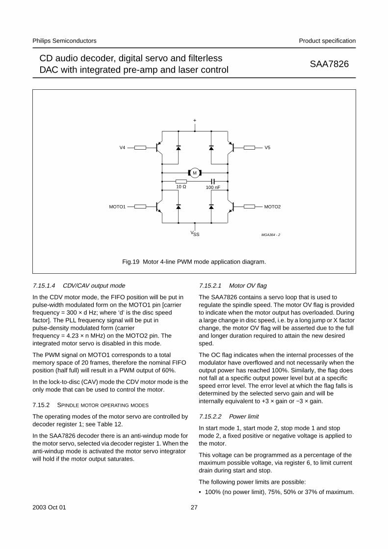
By using two extra outputs from the versatile pins interface, it is possible to use the SAA7826 with a 4-input motor bridge.The timing is illustrated in Fig 18. A typical application diagram is illustrated in Fig 19.
MOTO1
MOTO2
V4
V5
rept = 45 µs t 240 nsdead
ovlt = 240 ns
Accelerate Brake
MGA367 - 1
Fig.18 4-line PWM mode timing.
2003 Oct 01 27
Philips Semiconductors Product specification
CD audio decoder, digital servo and filterlessDAC with integrated pre-amp and laser control
SAA7826
MGA364 - 2VSS
+
M
MOTO1
V4
MOTO2
V5
100 nF10 Ω
Fig.19 Motor 4-line PWM mode application diagram.
7.15.1.4 CDV/CAV output mode
In the CDV motor mode, the FIFO position will be put inpulse-width modulated form on the MOTO1 pin [carrierfrequency = 300 × d Hz; where ‘d’ is the disc speedfactor]. The PLL frequency signal will be put inpulse-density modulated form (carrierfrequency = 4.23 × n MHz) on the MOTO2 pin. Theintegrated motor servo is disabled in this mode.
The PWM signal on MOTO1 corresponds to a totalmemory space of 20 frames, therefore the nominal FIFOposition (half full) will result in a PWM output of 60%.
In the lock-to-disc (CAV) mode the CDV motor mode is theonly mode that can be used to control the motor.
7.15.2 SPINDLE MOTOR OPERATING MODES
The operating modes of the motor servo are controlled bydecoder register 1; see Table 12.
In the SAA7826 decoder there is an anti-windup mode forthe motor servo, selected via decoder register 1. When theanti-windup mode is activated the motor servo integratorwill hold if the motor output saturates.
7.15.2.1 Motor OV flag
The SAA7826 contains a servo loop that is used toregulate the spindle speed. The motor OV flag is providedto indicate when the motor output has overloaded. Duringa large change in disc speed, i.e. by a long jump or X factorchange, the motor OV flag will be asserted due to the fulland longer duration required to attain the new desiredsped.
The OC flag indicates when the internal processes of themodulator have overflowed and not necessarily when theoutput power has reached 100%. Similarly, the flag doesnot fall at a specific output power level but at a specificspeed error level. The error level at which the flag falls isdetermined by the selected servo gain and will beinternally equivalent to +3 × gain or −3 × gain.
7.15.2.2 Power limit
In start mode 1, start mode 2, stop mode 1 and stopmode 2, a fixed positive or negative voltage is applied tothe motor.
This voltage can be programmed as a percentage of themaximum possible voltage, via register 6, to limit currentdrain during start and stop.
The following power limits are possible:
• 100% (no power limit), 75%, 50% or 37% of maximum.
2003 Oct 01 28
Philips Semiconductors Product specification
CD audio decoder, digital servo and filterlessDAC with integrated pre-amp and laser control
SAA7826
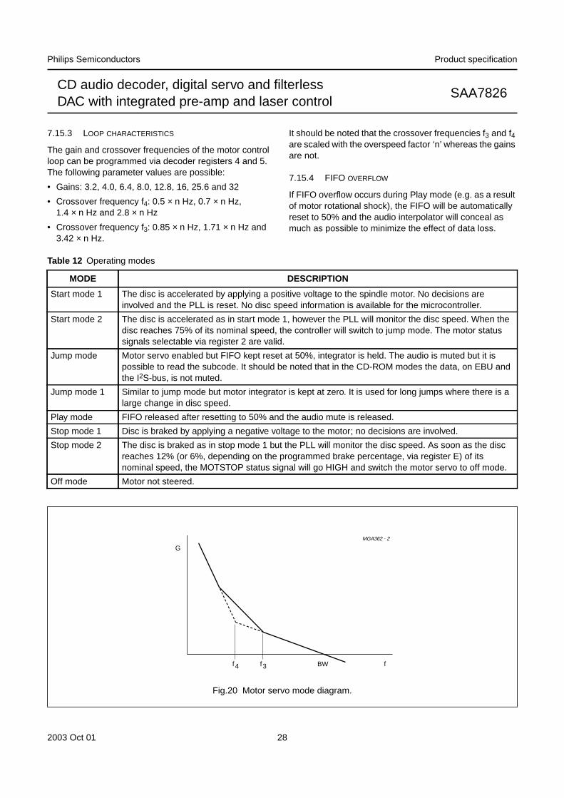
7.15.3 LOOP CHARACTERISTICS
The gain and crossover frequencies of the motor controlloop can be programmed via decoder registers 4 and 5.The following parameter values are possible:
• Gains: 3.2, 4.0, 6.4, 8.0, 12.8, 16, 25.6 and 32
• Crossover frequency f4: 0.5 × n Hz, 0.7 × n Hz,1.4 × n Hz and 2.8 × n Hz
• Crossover frequency f3: 0.85 × n Hz, 1.71 × n Hz and3.42 × n Hz.
It should be noted that the crossover frequencies f3 and f4are scaled with the overspeed factor ‘n’ whereas the gainsare not.
7.15.4 FIFO OVERFLOW
If FIFO overflow occurs during Play mode (e.g. as a resultof motor rotational shock), the FIFO will be automaticallyreset to 50% and the audio interpolator will conceal asmuch as possible to minimize the effect of data loss.
Table 12 Operating modes
MODE DESCRIPTION
Start mode 1 The disc is accelerated by applying a positive voltage to the spindle motor. No decisions areinvolved and the PLL is reset. No disc speed information is available for the microcontroller.
Start mode 2 The disc is accelerated as in start mode 1, however the PLL will monitor the disc speed. When thedisc reaches 75% of its nominal speed, the controller will switch to jump mode. The motor statussignals selectable via register 2 are valid.
Jump mode Motor servo enabled but FIFO kept reset at 50%, integrator is held. The audio is muted but it ispossible to read the subcode. It should be noted that in the CD-ROM modes the data, on EBU andthe I2S-bus, is not muted.
Jump mode 1 Similar to jump mode but motor integrator is kept at zero. It is used for long jumps where there is alarge change in disc speed.
Play mode FIFO released after resetting to 50% and the audio mute is released.
Stop mode 1 Disc is braked by applying a negative voltage to the motor; no decisions are involved.
Stop mode 2 The disc is braked as in stop mode 1 but the PLL will monitor the disc speed. As soon as the discreaches 12% (or 6%, depending on the programmed brake percentage, via register E) of itsnominal speed, the MOTSTOP status signal will go HIGH and switch the motor servo to off mode.
Off mode Motor not steered.
MGA362 - 2
G
f4f BW3f
Fig.20 Motor servo mode diagram.
2003 Oct 01 29
Philips Semiconductors Product specification
CD audio decoder, digital servo and filterlessDAC with integrated pre-amp and laser control
SAA7826
7.16 Servo part
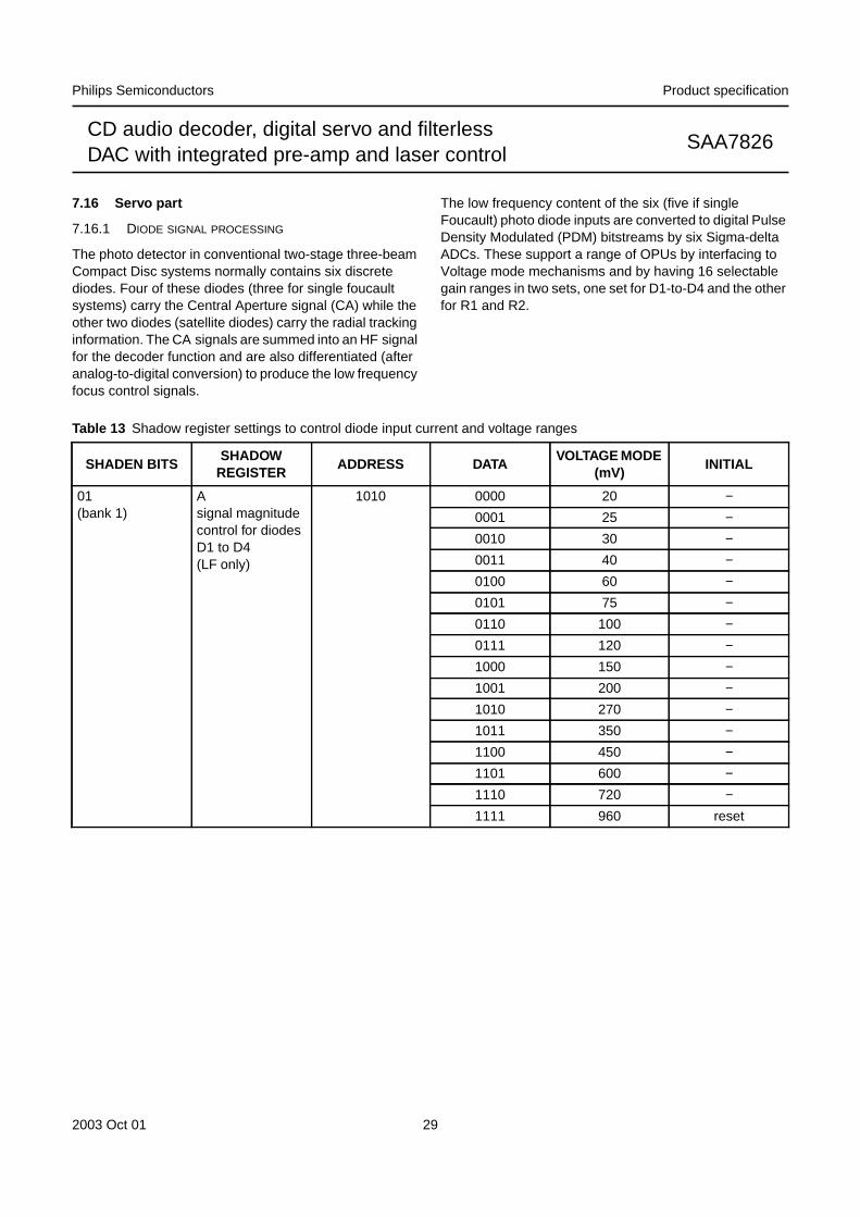
7.16.1 DIODE SIGNAL PROCESSING
The photo detector in conventional two-stage three-beamCompact Disc systems normally contains six discretediodes. Four of these diodes (three for single foucaultsystems) carry the Central Aperture signal (CA) while theother two diodes (satellite diodes) carry the radial trackinginformation. The CA signals are summed into an HF signalfor the decoder function and are also differentiated (afteranalog-to-digital conversion) to produce the low frequencyfocus control signals.
The low frequency content of the six (five if singleFoucault) photo diode inputs are converted to digital PulseDensity Modulated (PDM) bitstreams by six Sigma-deltaADCs. These support a range of OPUs by interfacing toVoltage mode mechanisms and by having 16 selectablegain ranges in two sets, one set for D1-to-D4 and the otherfor R1 and R2.
Table 13 Shadow register settings to control diode input current and voltage ranges
SHADEN BITSSHADOW
REGISTERADDRESS DATA
VOLTAGE MODE(mV)
INITIAL
01(bank 1)
Asignal magnitudecontrol for diodesD1 to D4(LF only)
1010 0000 20 −0001 25 −0010 30 −0011 40 −0100 60 −0101 75 −0110 100 −0111 120 −1000 150 −1001 200 −1010 270 −1011 350 −1100 450 −1101 600 −1110 720 −1111 960 reset
2003 Oct 01 30
Philips Semiconductors Product specification
CD audio decoder, digital servo and filterlessDAC with integrated pre-amp and laser control
SAA7826
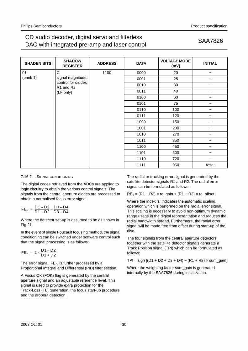
01(bank 1)
Csignal magnitudecontrol for diodesR1 and R2(LF only)
1100 0000 20 −0001 25 −0010 30 −0011 40 −0100 60 −0101 75 −0110 100 −0111 120 −1000 150 −1001 200 −1010 270 −1011 350 −1100 450 −1101 600 −1110 720 −1111 960 reset
SHADEN BITSSHADOW
REGISTERADDRESS DATA
VOLTAGE MODE(mV)
INITIAL
7.16.2 SIGNAL CONDITIONING
The digital codes retrieved from the ADCs are applied tologic circuitry to obtain the various control signals. Thesignals from the central aperture diodes are processed toobtain a normalised focus error signal:
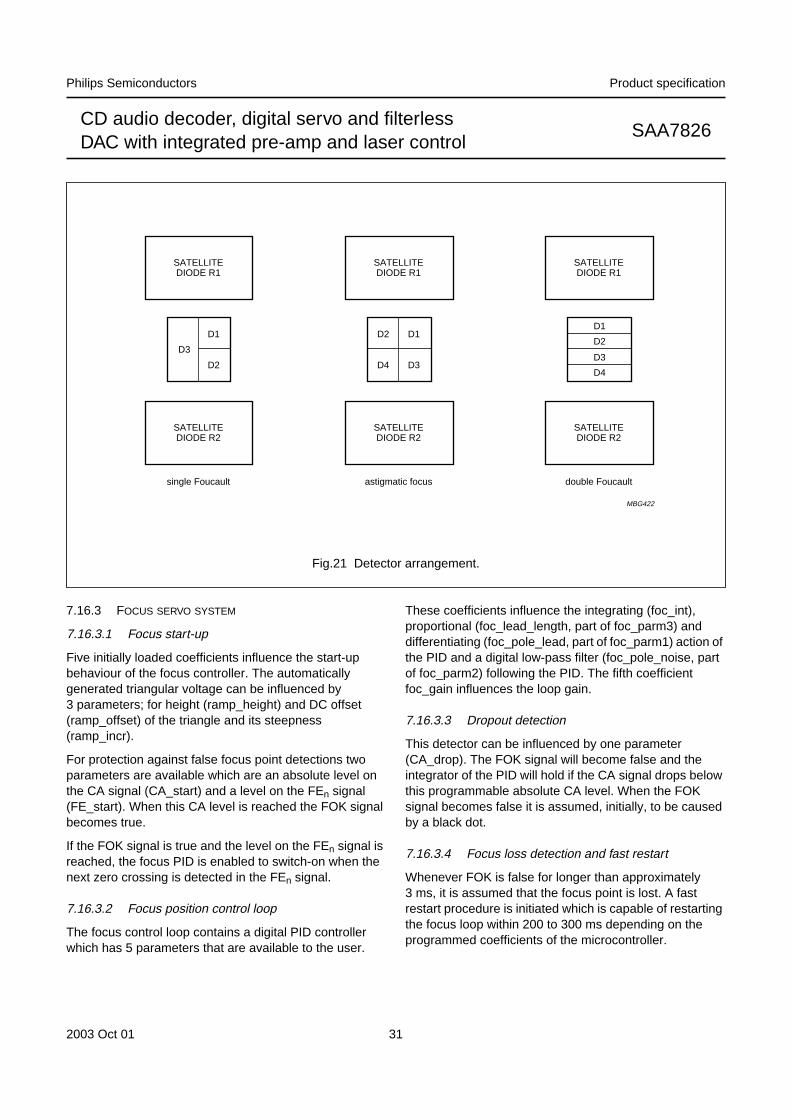
Where the detector set-up is assumed to be as shown inFig 21.
In the event of single Foucault focusing method, the signalconditioning can be switched under software control suchthat the signal processing is as follows:
The error signal, FEn, is further processed by aProportional Integral and Differential (PID) filter section.
A Focus OK (FOK) flag is generated by the centralaperture signal and an adjustable reference level. Thissignal is used to provide extra protection for theTrack-Loss (TL) generation, the focus start-up procedureand the dropout detection.
The radial or tracking error signal is generated by thesatellite detector signals R1 and R2. The radial errorsignal can be formulated as follows:
REs = (R1 − R2) × re_gain + (R1 + R2) × re_offset.
Where the index ‘s’ indicates the automatic scalingoperation which is performed on the radial error signal.This scaling is necessary to avoid non-optimum dynamicrange usage in the digital representation and reduces theradial bandwidth spread. Furthermore, the radial errorsignal will be made free from offset during start-up of thedisc.
The four signals from the central aperture detectors,together with the satellite detector signals generate aTrack Position signal (TPI) which can be formulated asfollows:
TPI = sign [(D1 + D2 + D3 + D4) − (R1 + R2) × sum_gain]
Where the weighting factor sum_gain is generatedinternally by the SAA7826 during initialization.
FEnD1 D2–D1 D2+----------------------
D3 D4–D3 D4+----------------------–=
FEn 2D1 D2–D1 D2+----------------------×=
2003 Oct 01 31
Philips Semiconductors Product specification
CD audio decoder, digital servo and filterlessDAC with integrated pre-amp and laser control
SAA7826
handbook, full pagewidth
D3
D1
D2
SATELLITEDIODE R1
SATELLITEDIODE R2
D1
D3
D2
D4
SATELLITEDIODE R1
SATELLITEDIODE R2
D1
D2
D3
D4
SATELLITEDIODE R1
SATELLITEDIODE R2
single Foucault astigmatic focus double Foucault
MBG422
Fig.21 Detector arrangement.
7.16.3 FOCUS SERVO SYSTEM
7.16.3.1 Focus start-up
Five initially loaded coefficients influence the start-upbehaviour of the focus controller. The automaticallygenerated triangular voltage can be influenced by3 parameters; for height (ramp_height) and DC offset(ramp_offset) of the triangle and its steepness(ramp_incr).
For protection against false focus point detections twoparameters are available which are an absolute level onthe CA signal (CA_start) and a level on the FEn signal(FE_start). When this CA level is reached the FOK signalbecomes true.
If the FOK signal is true and the level on the FEn signal isreached, the focus PID is enabled to switch-on when thenext zero crossing is detected in the FEn signal.
7.16.3.2 Focus position control loop
The focus control loop contains a digital PID controllerwhich has 5 parameters that are available to the user.
These coefficients influence the integrating (foc_int),proportional (foc_lead_length, part of foc_parm3) anddifferentiating (foc_pole_lead, part of foc_parm1) action ofthe PID and a digital low-pass filter (foc_pole_noise, partof foc_parm2) following the PID. The fifth coefficientfoc_gain influences the loop gain.
7.16.3.3 Dropout detection
This detector can be influenced by one parameter(CA_drop). The FOK signal will become false and theintegrator of the PID will hold if the CA signal drops belowthis programmable absolute CA level. When the FOKsignal becomes false it is assumed, initially, to be causedby a black dot.
7.16.3.4 Focus loss detection and fast restart
Whenever FOK is false for longer than approximately3 ms, it is assumed that the focus point is lost. A fastrestart procedure is initiated which is capable of restartingthe focus loop within 200 to 300 ms depending on theprogrammed coefficients of the microcontroller.
2003 Oct 01 32
Philips Semiconductors Product specification
CD audio decoder, digital servo and filterlessDAC with integrated pre-amp and laser control
SAA7826
7.16.3.5 Focus loop gain switching
The gain of the focus control loop (foc_gain) can bemultiplied by a factor of 2 or divided by a factor of 2 duringnormal operation. The integrator value of the PID iscorrected accordingly. The differentiating (foc_pole_lead)action of the PID can be switched at the same time as thegain switching is performed.
7.16.3.6 Focus automatic gain control loop
The loop gain of the focus control loop can be correctedautomatically to eliminate tolerances in the focus loop.This gain control injects a signal into the loop which is usedto correct the loop gain. Since this decreases the optimumperformance, the gain control should only be activated fora short time (for example, when starting a new disc).
7.16.4 RADIAL SERVO SYSTEM
7.16.4.1 Level initialization
During start-up an automatic adjustment procedure isactivated to set the values of the radial error gain (re_gain),offset (re_offset) and satellite sum gain (sum_gain) for TPIlevel generation. The initialization procedure runs in aradial open loop situation and is ≤300 ms. This start-uptime period may coincide with the last part of the motorstart-up time period:
• Automatic gain adjustment: as a result of thisinitialization the amplitude of the RE signal is adjusted towithin ±10% around the nominal RE amplitude
• Offset adjustment: the additional offset in RE due to thelimited accuracy of the start-up procedure is less than±50 nm
• TPI level generation: the accuracy of the initializationprocedure is such that the duty factor range of TPIbecomes 0.4 < duty factor < 0.6 (default dutyfactor = TPI HIGH/TPI period).
7.16.4.2 Sledge control
The microcontroller can move the sledge in both directionsvia the steer sledge command.
7.16.4.3 Tracking control
The actuator is controlled using a PID loop filter with userdefined coefficients and gain. For stable operationbetween the tracks, the S-curve is extended over 75% ofthe track. On request from the microcontroller, S-curveextension over 2.25 tracks is used, automatically changingto access control when exceeding those 2.25 tracks.
Both modes of S-curve extension make use of atrack-count mechanism. In this mode, track countingresults in an ‘automatic return-to-zero track’, to avoidmajor disturbances in the audio output and providingimproved shock resistance. The sledge is continuouslycontrolled, or provided with step pulses to reduce powerconsumption using the filtered value of the radial PIDoutput. Alternatively, the microcontroller can read theaverage voltage on the radial actuator and provide thesledge with step pulses to reduce power consumption.Filter coefficients of the continuous sledge control can bepreset by the user.
7.16.4.4 Access
The access procedure is divided into two different modes(see Table 14), depending on the requested jump size.
Table 14 Access modes
Note
1. The microcontroller can be preset.
The access procedure makes use of a track countingmechanism, a velocity signal based on a fixed number oftracks passed within a fixed time interval, a velocity setpoint calculated from the number of tracks to go and a userprogrammable parameter indicating the maximum sledgeperformance.
If the number of tracks remaining is greater than thebrake_distance then the sledge jump mode should beactivated or, the actuator jump should be performed. Therequested jump size together with the required sledgebreaking distance at maximum access speed defines thebrake_distance value.
During the actuator jump mode, velocity control with a PIcontroller is used for the actuator. The sledge is thencontinuously controlled using the filtered value of the radialPID output. All filter parameters (for actuator and sledge)are user programmable.
ACCESSTYPE
JUMP SIZE(1) ACCESSSPEED
Actuator jump 1 − brake_distance decreasingvelocity
Sledge jump brake_distance −32768 maximumpower tosledge(1)
2003 Oct 01 33
Philips Semiconductors Product specification
CD audio decoder, digital servo and filterlessDAC with integrated pre-amp and laser control
SAA7826
In the sledge jump mode maximum power (userprogrammable) is applied to the sledge in the correctdirection while the actuator becomes idle (the content ofthe actuator integrator leaks to zero just after the sledgejump mode is initiated). The actuator can be electronicallydamped during sledge jump. The gain of the damping loopis controlled via the hold_mult parameter.
The fast track jumping circuitry can be enabled or disabledvia the xtra_preset parameter.
7.16.4.5 Radial automatic gain control loop
The loop gain of the radial control loop can be correctedautomatically to eliminate tolerances in the radial loop.This gain control injects a signal into the loop which is usedto correct the loop gain. Since this decreases the optimumperformance, the gain control should only be activated fora short time (for example, when starting a new disc).
This gain control differs from the level initialization. Thelevel initialization should be performed first. Thedisadvantage of using the level initialization without thegain control is that only tolerances from the front-end arereduced.
7.16.5 OFF-TRACK COUNTING
The Track Position signal (TPI) is a flag which is used toindicate whether the radial spot is positioned on the track,with a margin of ±0.25 of the track pitch. In combinationwith the Radial Polarity flag (RP) the relative spot positionover the tracks can be determined.
These signals can have uncertainties caused by:
• Disc defects such as scratches and fingerprints
• The HF information on the disc, which is considered asnoise by the detector signals.
In order to determine the spot position with sufficientaccuracy, extra conditions are necessary to generate aTrack Loss signal (TL) and an off-track counter value.These extra conditions influence the maximum speed andthis implies that, internally, one of the following threecounting states is selected:
1. Protected state: used in normal play situations. A goodprotection against false detection caused by discdefects is important in this state.
2. Slow counting state: used in low velocity track jumpsituations. In this state a fast response is importantrather than the protection against disc defects (if thephase relationship between TL and RP of 0.5π radiansis affected too much, the direction cannot then bedetermined accurately).
3. Fast counting state: used in high velocity track jumpsituations. Highest obtainable velocity is the mostimportant feature in this state.
7.16.6 TRACK COUNTING MODES
Fast counting mode is auto-selected for track-crossingspeeds above 1200 tracks/s. In this case the off-trackcounting decrements occur only for effect of the RP signal.The direction of the jump is already known because theSlow counting mode occurs prior to entering the Fastcounting mode.
When the Slow counting mode is selected the maximumtrack-crossing speed that can be reached is 12 kHz(providing that the maximum value for rad_pole_lead isused). In this case the direction of the jump is given by thephase shift between RP and TL(+90o for outward jumpsand -90o for inward jumps). The number of pulses in the TLsignal gives the number of tracks crossed.
When Fast counting mode is enabled, whenever thetrack-crossing speed falls below 12 kHz, the countingmode is automatically changed to Slow counting mode.
7.16.7 DEFECT DETECTION
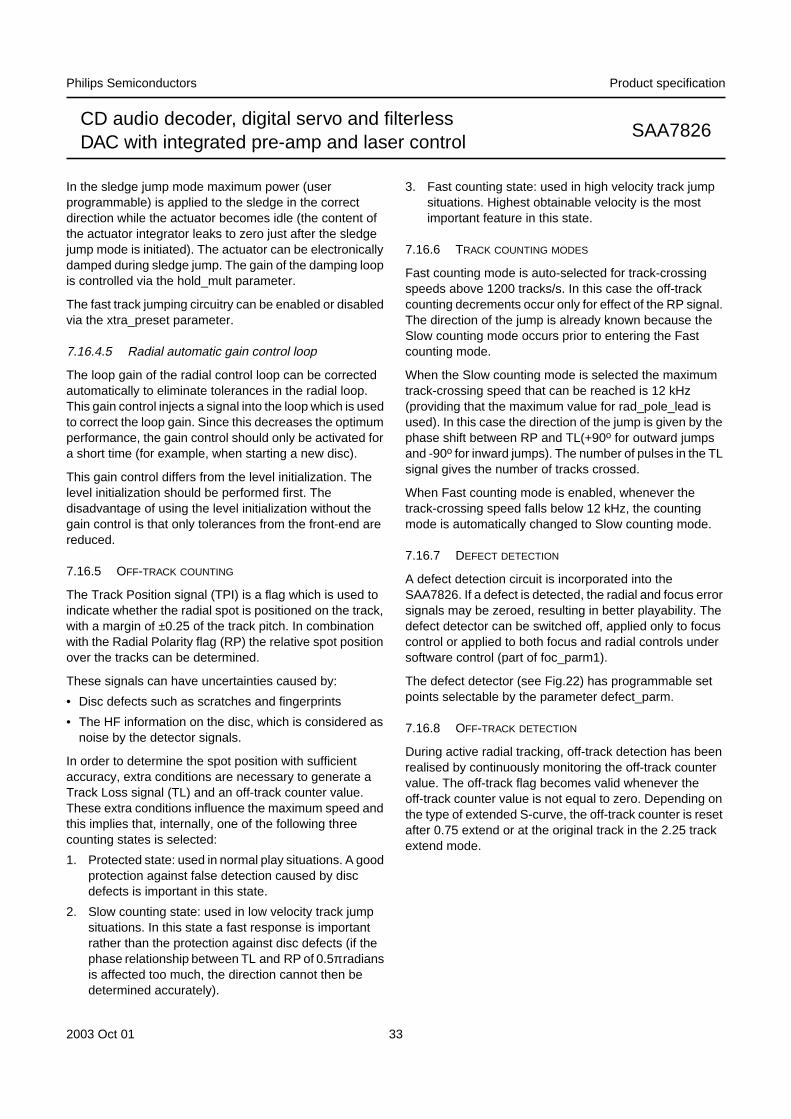
A defect detection circuit is incorporated into theSAA7826. If a defect is detected, the radial and focus errorsignals may be zeroed, resulting in better playability. Thedefect detector can be switched off, applied only to focuscontrol or applied to both focus and radial controls undersoftware control (part of foc_parm1).
The defect detector (see Fig.22) has programmable setpoints selectable by the parameter defect_parm.
7.16.8 OFF-TRACK DETECTION
During active radial tracking, off-track detection has beenrealised by continuously monitoring the off-track countervalue. The off-track flag becomes valid whenever theoff-track counter value is not equal to zero. Depending onthe type of extended S-curve, the off-track counter is resetafter 0.75 extend or at the original track in the 2.25 trackextend mode.
2003 Oct 01 34
Philips Semiconductors Product specification
CD audio decoder, digital servo and filterlessDAC with integrated pre-amp and laser control
SAA7826
handbook, full pagewidth
DECIMATIONFILTER
FASTFILTER
DEFECTGENERATION
PROGRAMMABLEHOLD-OFF
SLOWFILTER
defectoutputsat1
sat2
+
−
MBG421
Fig.22 Block diagram of the defect detector.
7.16.9 HIGH-LEVEL FEATURES
7.16.9.1 Interrupt mechanism and STATUS pin
The STATUS pin is an output which can be configured bydecoder register 7 and new shadow register C (bank 3) forone of three different modes of operation. These are:
• Output the interrupt signal generated by the servo part(it should be noted that the selection of this mode willoverride all other modes)
• Output the decoder status bit (active LOW) selected bydecoder register 2 (only available in 4-wire bus mode)
• Output DC offset information (it should be noted that thismode is used in conjunction with the decoder statusmode; see Section 7.5).
Eight signals from the interrupt status register areselectable from the servo part via the interrupt_maskparameter. The interrupt is reset by sending the readhigh-level status command. The 8 signals are as follows:
• Focus lost: dropout of longer than 3 ms
• Subcode ready
• Subcode absolute seconds changed
• Subcode discontinuity detected: new subcode timebefore previous subcode time, or more than 10 frameslater than previous subcode time
• Radial error: during radial on-track, no new subcodeframe occurs within the time defined by the‘playwatchtime’ parameter; during radial jump, less than4 tracks have been crossed during the time defined bythe ‘jumpwatchtime’ parameter
• Autosequencer state change
• Autosequencer error
• Subcode interface blocked: the internal decoderinterface is being used.
It should be noted that if the STATUS pin is configured tooutput decoder status information [decoder register7 = XX10 and new shadow register C (bank 3) = X00X]and either the microcontroller writes a different value todecoder register 2 or the decoder interface is enabled thenthe STATUS output will change.
7.16.9.2 Decoder interface
The decoder interface allows decoder and shadowregisters to be programmed and subcode Q-channel datato be read via servo commands. The interface is enabledor disabled by the preset latch command (and thextra_preset parameter).
7.16.9.3 Automatic error handling
Three Watchdogs are present:
• Focus: detects focus dropout of longer than 3 ms, setsfocus lost interrupt, switches off radial and sledgeservos and disables the drive-to-disc motor
• Radial play: started when radial servo is in on-trackmode and a first subcode frame is found; detects whenthe maximum time between two subcode framesexceeds the time set by the playwatchtime parameter; itthen sets the radial error interrupt, switches radial andsledge servos off and puts the disc motor into jumpmode
• Radial jump: active when radial servo is in long jump orshort jump modes; detects when the off-track countervalue decreases by less than 4 tracks between tworeadings (the time interval is set by the jumpwatchtimeparameter); it then sets the radial jump error, switchesradial and sledge servos off to cancel jump.
The focus Watchdog is always active, the radialWatchdogs are selectable via the radcontrol parameter.
2003 Oct 01 35
Philips Semiconductors Product specification
CD audio decoder, digital servo and filterlessDAC with integrated pre-amp and laser control
SAA7826
7.16.9.4 Automatic sequencers and timer interrupts
Two automatic sequencers are implemented (and must beinitialized after power-on):
• Auto-start sequencer: controls the start-up of focus,radial and motor
• Auto-stop sequencer: brakes the disc and shuts downthe servos.
When the automatic sequencers are not used it is possibleto generate timer interrupts, defined by thetime_parameter coefficient.
7.16.9.5 High-level status
The read high-level status command can be used to obtainthe interrupt, decoder, autosequencer status registers andthe motor start time. Use of the read high-level statuscommand clears the interrupt status register, andre-enables the subcode read via a servo command.
7.16.10 DRIVER INTERFACE
The control signals (pins RA, FO and SL) for themechanism actuators are pulse density modulated. Themodulating frequency can be set to either 1.0584 or2.1168 MHz; controlled via the xtra_preset parameter.An analog representation of the output signals can beachieved by connecting a 1st-order low-pass filter to theoutputs.
During reset (i.e. RESET pin is held LOW) the RA, FO andSL pins are high-impedance. At all other times, when thelaser is switched off, the RA and FO pins output a 2 MHz50% duty factor signal.
7.16.11 LASER INTERFACE
The laser diode pre-amplifier function is built into theSAA7826; see Fig.23. The current can be regulated, up to120 mA [programmed via new shadow register A (bank 2)and register 3 (bank 3)], in four steps ranging from 58% upto full power. New shadow register A (bank 2) andregister 3 (bank 3)] are used to select the step values.
The voltage derived from the monitor diode is maintainedat a steady state by the laser drive circuitry, by regulatingthe current through the laser diode. The type of monitordiode being used (150 mV or 180 mV) must be selected bynew shadow register 7 (bank 2) (reset state = 150 mV).
The laser can be switched on or off by the xtra_presetparameter; it is automatically driven if the focus controlloop is active.
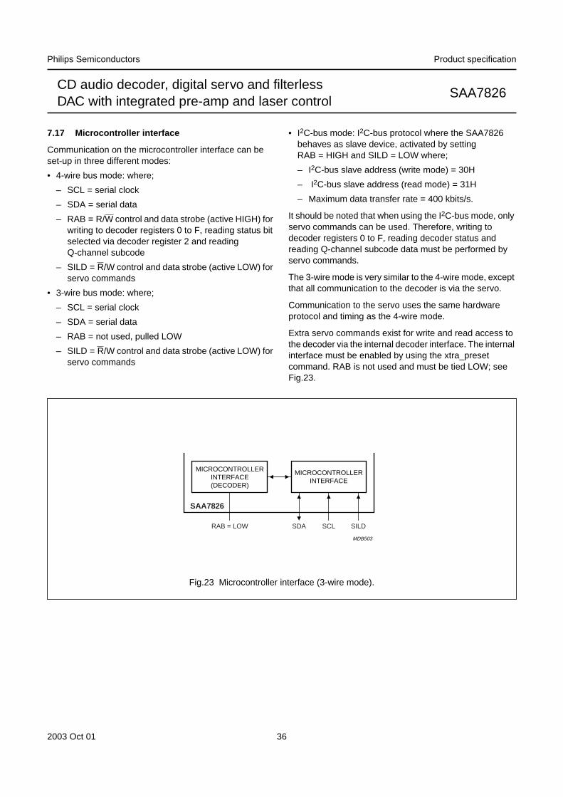
2003 Oct 01 36
Philips Semiconductors Product specification
CD audio decoder, digital servo and filterlessDAC with integrated pre-amp and laser control
SAA7826
7.17 Microcontroller interface
Communication on the microcontroller interface can beset-up in three different modes:
• 4-wire bus mode: where;
– SCL = serial clock
– SDA = serial data
– RAB = R/W control and data strobe (active HIGH) forwriting to decoder registers 0 to F, reading status bitselected via decoder register 2 and readingQ-channel subcode
– SILD = R/W control and data strobe (active LOW) forservo commands
• 3-wire bus mode: where;
– SCL = serial clock
– SDA = serial data
– RAB = not used, pulled LOW
– SILD = R/W control and data strobe (active LOW) forservo commands
• I2C-bus mode: I2C-bus protocol where the SAA7826behaves as slave device, activated by settingRAB = HIGH and SILD = LOW where;
– I2C-bus slave address (write mode) = 30H
– I2C-bus slave address (read mode) = 31H
– Maximum data transfer rate = 400 kbits/s.
It should be noted that when using the I2C-bus mode, onlyservo commands can be used. Therefore, writing todecoder registers 0 to F, reading decoder status andreading Q-channel subcode data must be performed byservo commands.
The 3-wire mode is very similar to the 4-wire mode, exceptthat all communication to the decoder is via the servo.
Communication to the servo uses the same hardwareprotocol and timing as the 4-wire mode.
Extra servo commands exist for write and read access tothe decoder via the internal decoder interface. The internalinterface must be enabled by using the xtra_presetcommand. RAB is not used and must be tied LOW; seeFig.23.
handbook, halfpage
MDB503
MICROCONTROLLERINTERFACE(DECODER)
MICROCONTROLLERINTERFACE
SAA7826
RAB = LOW SDA SCL SILD
Fig.23 Microcontroller interface (3-wire mode).
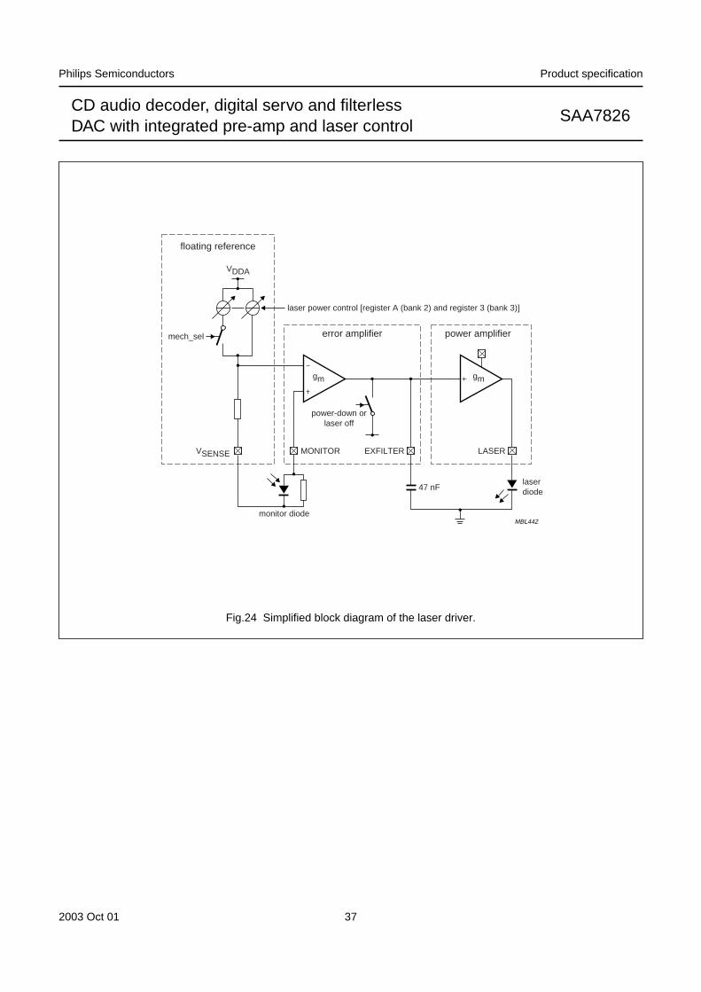
2003 Oct 01 37
Philips Semiconductors Product specification
CD audio decoder, digital servo and filterlessDAC with integrated pre-amp and laser control
SAA7826
handbook, full pagewidth
MBL442
MONITOR
laser power control [register A (bank 2) and register 3 (bank 3)]
mech_sel
laserdiode47 nF
monitor diode
EXFILTER LASER
error amplifier
floating reference
power amplifier
power-down orlaser off
gm
VDDA
gm
VSENSE
Fig.24 Simplified block diagram of the laser driver.
2003 Oct 01 38
Philips Semiconductors Product specification
CD audio decoder, digital servo and filterlessDAC with integrated pre-amp and laser control
SAA7826
7.17.1 MICROCONTROLLER INTERFACE (4-WIRE BUS MODE)
7.17.1.1 Writing data to registers 0 to F
The sixteen 4-bit programmable configuration registers,0 to F (see Table 15), can be written to via themicrocontroller interface using the protocol shown inFig.25. It should be noted that SILD must be held HIGH;A3 to A0 identifies the register number and D3 to D0 is thedata. The data is latched into the register on theLOW-to-HIGH transition of RAB.
7.17.1.2 Writing repeated data to registers 0 to F
The same data can be repeated several times (e.g. for afade function) by applying extra RAB pulses as shown inFig.26. It should be noted that SCL must stay HIGHbetween RAB pulses.
7.17.1.3 Multiple writes to the new shadow registers
Some of the new shadow registers are a multiple of fourbits in length and require a number of write operations tofill them up; see Section 7.17.5. They must be completelyfilled before writing to another register, otherwiseunpredictable behaviour may result.
The protocol for writing to these registers is exactly thesame as the decoder registers; see Fig.25. The writecommand must be executed multiple times with the sameaddress content. The first four bits of data in a sequenceof write commands represent the most significant nibble ofthe register, while the last four represent the leastsignificant nibble. The data content can change from onewrite to the next without consequence.
7.17.1.4 Reading decoder status information on SDA
There are several internal status signals, selected viaregister 2, which can be made available on the SDA line:
• SUBQREADY-I: LOW if new subcode word is ready inQ-channel register
• MOTSTART1: HIGH if motor is turning at 75% or moreof nominal speed
• MOTSTART2: HIGH if motor is turning at 50% or moreof nominal speed
• MOTSTOP: HIGH if motor is turning at 12% or less ofnominal speed; can be set to indicate 6% or less(instead of 12% or less) via register E
• PLL lock: HIGH if sync coincidence signals are found
• V1: follows input on pin V1
• V2: follows input on pin V2
• MOTOR-OV: HIGH if the motor servo output stagesaturates.
The status read protocol is illustrated in Fig.27. It should benoted that SILD must be held HIGH.
7.17.1.5 Reading Q-channel subcode
To read the Q-channel subcode direct in the 4-wire busmode, the SUBQREADY-I signal should be selected asthe status signal. The subcode read protocol is illustratedin Fig.28.
It should be noted that SILD must be held HIGH; aftersubcode read starts, the microcontroller may take as longas it wants to terminate the read operation. When enoughsubcode has been read (1 to 96 bits), the reading can beterminated by pulling RAB LOW.
Alternatively, the Q-channel subcode can be read using aservo command as follows:
• Use the read high-level status command to monitor thesubcode ready signal
• Send the read subcode command and read the requirednumber of bytes (up to 12)
• Send the read HIGH-level status command; to re-enablethe decoder interface.
7.17.1.6 Behaviour of the SUBQREADY-I signal
When the CRC of the Q-channel word is good, and nosubcode is being read, the SUBQREADY-I status signalwill react as illustrated in Fig.29. When the CRC is goodand the subcode is being read, the timing in Fig.30 applies.
If t1 (SUBQREADY-I status LOW to end of subcode read)is below 2.6/n ms, then t2 = 13.1/n ms (i.e. themicrocontroller can read all subcode frames if it completesthe read operation within 2.6/n ms after the subcode isready). If these criteria are not met, it is only possible toguarantee that t3 will be below 26.2/n ms (approximately).
If subcode frames with failed CRCs are present, thet2 and t3 times will be increased by 13.1/n ms for eachdefective subcode frame.
It should be noted that in the lock-to-disc mode ‘n’ isreplaced by ‘d’, which is the disc speed factor.
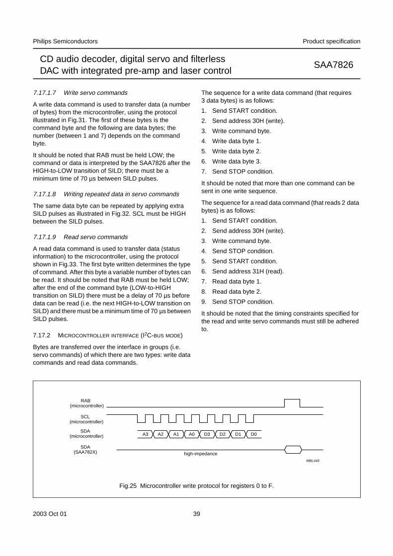
2003 Oct 01 39
Philips Semiconductors Product specification
CD audio decoder, digital servo and filterlessDAC with integrated pre-amp and laser control
SAA7826
7.17.1.7 Write servo commands
A write data command is used to transfer data (a numberof bytes) from the microcontroller, using the protocolillustrated in Fig.31. The first of these bytes is thecommand byte and the following are data bytes; thenumber (between 1 and 7) depends on the commandbyte.
It should be noted that RAB must be held LOW; thecommand or data is interpreted by the SAA7826 after theHIGH-to-LOW transition of SILD; there must be aminimum time of 70 µs between SILD pulses.
7.17.1.8 Writing repeated data in servo commands
The same data byte can be repeated by applying extraSILD pulses as illustrated in Fig.32. SCL must be HIGHbetween the SILD pulses.
7.17.1.9 Read servo commands
A read data command is used to transfer data (statusinformation) to the microcontroller, using the protocolshown in Fig.33. The first byte written determines the typeof command. After this byte a variable number of bytes canbe read. It should be noted that RAB must be held LOW;after the end of the command byte (LOW-to-HIGHtransition on SILD) there must be a delay of 70 µs beforedata can be read (i.e. the next HIGH-to-LOW transition onSILD) and there must be a minimum time of 70 µs betweenSILD pulses.
7.17.2 MICROCONTROLLER INTERFACE (I2C-BUS MODE)
Bytes are transferred over the interface in groups (i.e.servo commands) of which there are two types: write datacommands and read data commands.
The sequence for a write data command (that requires3 data bytes) is as follows:
1. Send START condition.
2. Send address 30H (write).
3. Write command byte.
4. Write data byte 1.
5. Write data byte 2.
6. Write data byte 3.
7. Send STOP condition.
It should be noted that more than one command can besent in one write sequence.
The sequence for a read data command (that reads 2 databytes) is as follows:
1. Send START condition.
2. Send address 30H (write).
3. Write command byte.
4. Send STOP condition.
5. Send START condition.
6. Send address 31H (read).
7. Read data byte 1.
8. Read data byte 2.
9. Send STOP condition.
It should be noted that the timing constraints specified forthe read and write servo commands must still be adheredto.
handbook, full pagewidth
A3 A2 A1 A0 D3 D2 D1 D0
SDA(SAA782X)
SCL (microcontroller)
RAB (microcontroller)
SDA (microcontroller)
MBL445
high-impedance
Fig.25 Microcontroller write protocol for registers 0 to F.
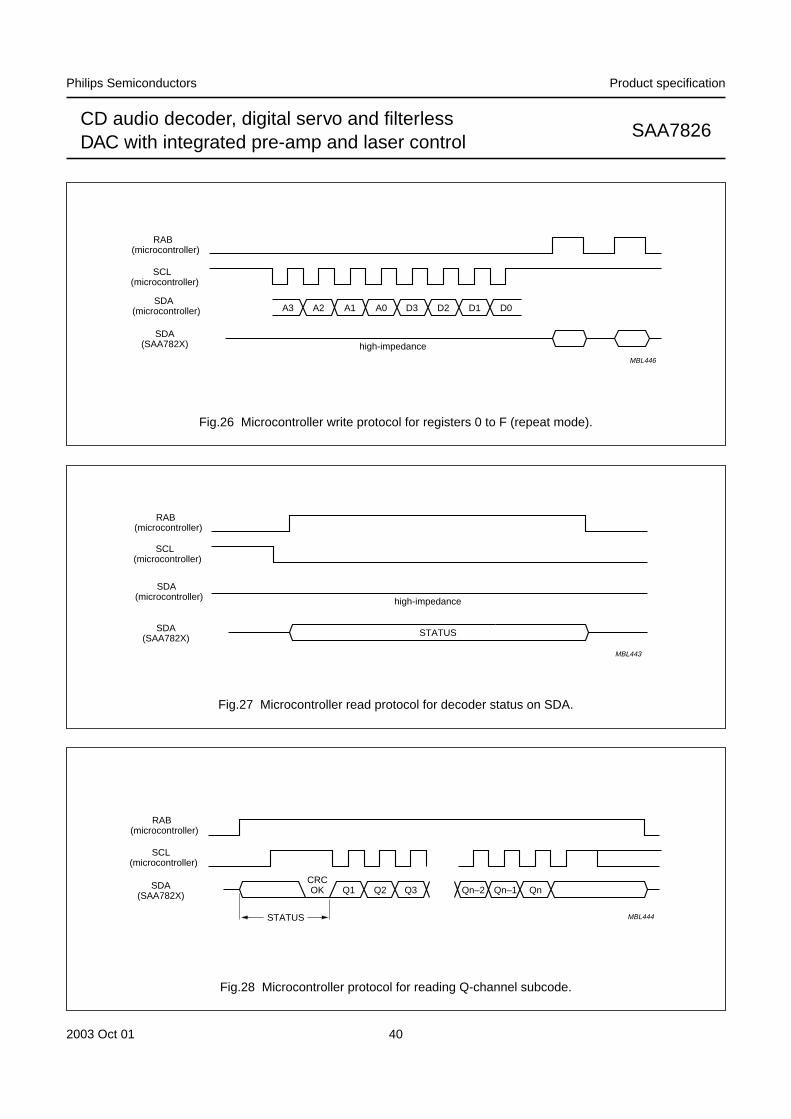
2003 Oct 01 40
Philips Semiconductors Product specification
CD audio decoder, digital servo and filterlessDAC with integrated pre-amp and laser control
SAA7826
handbook, full pagewidth
A3 A2 A1 A0 D3 D2 D1 D0
SDA(SAA782X)
MBL446
SCL (microcontroller)
RAB (microcontroller)
SDA (microcontroller)
high-impedance
Fig.26 Microcontroller write protocol for registers 0 to F (repeat mode).
handbook, full pagewidth
SDA(SAA782X)
MBL443
STATUS
SCL (microcontroller)
RAB (microcontroller)
SDA (microcontroller) high-impedance
Fig.27 Microcontroller read protocol for decoder status on SDA.
handbook, full pagewidth
Q1 Q2 Q3 Qn–1SDA(SAA782X)
MBL444
Qn–2 Qn
STATUS
CRCOK
SCL (microcontroller)
RAB (microcontroller)
Fig.28 Microcontroller protocol for reading Q-channel subcode.
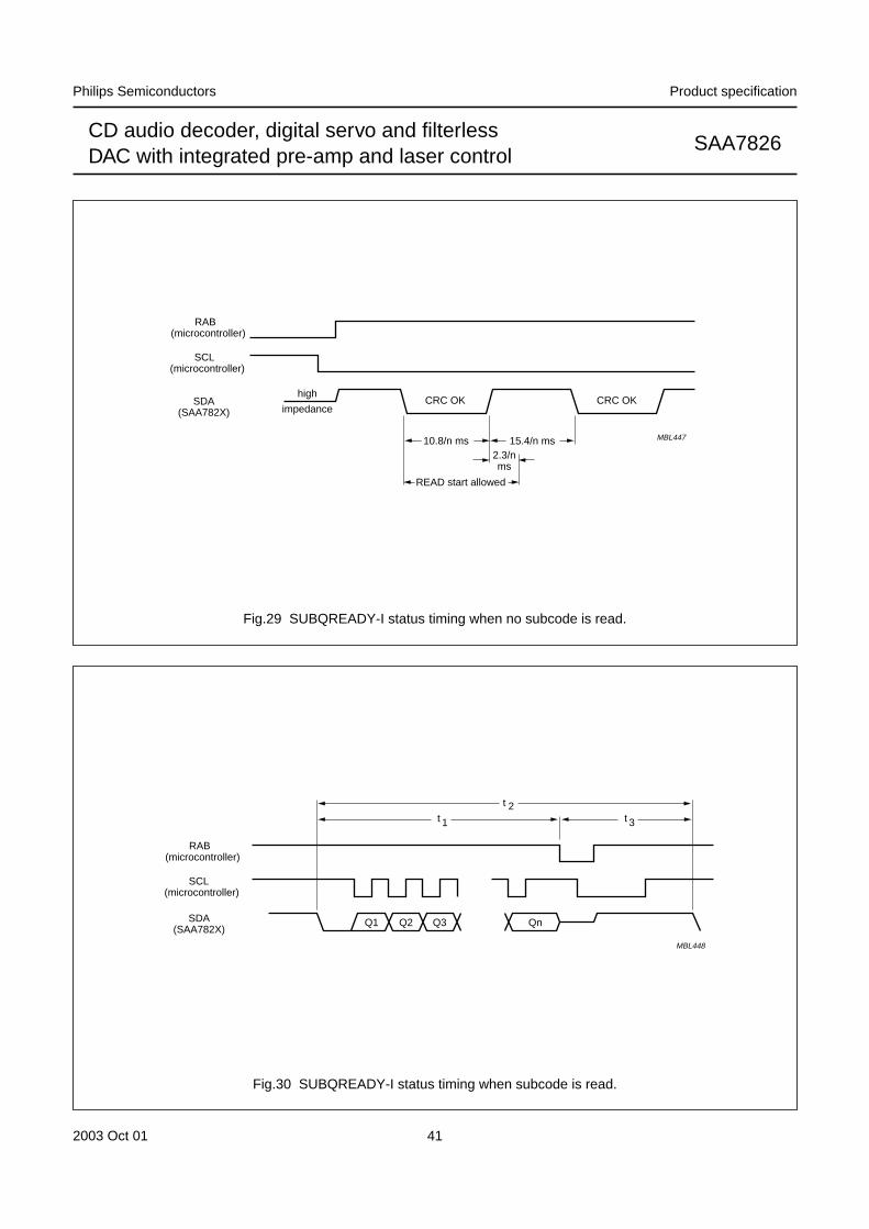
2003 Oct 01 41
Philips Semiconductors Product specification
CD audio decoder, digital servo and filterlessDAC with integrated pre-amp and laser control
SAA7826
handbook, full pagewidth
SDA(SAA782X)
10.8/n ms 15.4/n ms2.3/nms
READ start allowed
high
impedanceCRC OK CRC OK
MBL447
SCL (microcontroller)
RAB (microcontroller)
Fig.29 SUBQREADY-I status timing when no subcode is read.
handbook, full pagewidth
Q1 Q2 Q3 QnSDA(SAA782X)
t 1
t 2t 3
MBL448
SCL (microcontroller)
RAB (microcontroller)
Fig.30 SUBQREADY-I status timing when subcode is read.
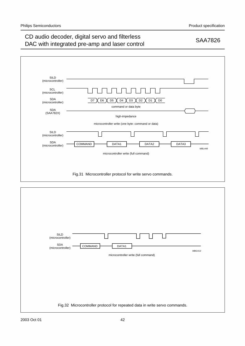
2003 Oct 01 42
Philips Semiconductors Product specification
CD audio decoder, digital servo and filterlessDAC with integrated pre-amp and laser control
SAA7826
handbook, full pagewidth
D7 D6 D5 D4 D3 D2 D1 D0
SDA(SAA782X)
SILD(microcontroller)
SCL (microcontroller)
SDA(microcontroller)
SILD(microcontroller)
SDA(microcontroller) COMMAND DATA1 DATA2 DATA3
command or data byte
high-impedance
microcontroller write (one byte: command or data)
microcontroller write (full command)
MBL449
Fig.31 Microcontroller protocol for write servo commands.
handbook, full pagewidth
SILD(microcontroller)
SDA(microcontroller)
microcontroller write (full command)
COMMAND DATA1
MBG413
Fig.32 Microcontroller protocol for repeated data in write servo commands.
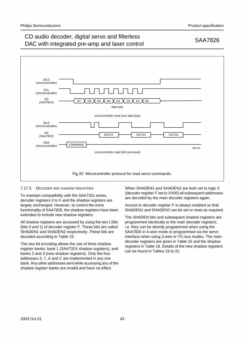
2003 Oct 01 43
Philips Semiconductors Product specification
CD audio decoder, digital servo and filterlessDAC with integrated pre-amp and laser control
SAA7826
handbook, full pagewidth
DATA1 DATA2 DATA3
COMMAND
SILD(microcontroller)
SILD(microcontroller)
SCL(microcontroller)
SDA(microcontroller)
SD(SAA782X)
SD(SAA782X) D7 D6 D5 D4 D3 D2 D1 D0
data byte
microcontroller read (one data byte)
microcontroller read (full command)
MBL450
Fig.33 Microcontroller protocol for read servo commands.
7.17.3 DECODER AND SHADOW REGISTERS
To maintain compatibility with the SAA732x series,decoder registers 0 to F and the shadow registers arelargely unchanged. However, to control the extrafunctionality of SAA7826, the shadow registers have beenextended to include new shadow registers.
All shadow registers are accessed by using the two LSBs(bits 0 and 1) of decoder register F. These bits are calledSHADEN1 and SHADEN2 respectively. These bits aredecoded according to Table 15.
This two bit encoding allows the use of three shadowregister banks; bank 1 (SAA732X shadow registers), andbanks 2 and 3 (new shadow registers). Only the fouraddresses 3, 7, A and C are implemented in any onebank. Any other addresses sent while accessing any of theshadow register banks are invalid and have no effect.
When SHADEN1 and SHADEN2 are both set to logic 0(decoder register F set to XX00) all subsequent addressesare decoded by the main decoder registers again.
Access to decoder register F is always enabled so thatSHADEN1 and SHADEN2 can be set or reset as required.
The SHADEN bits and subsequent shadow registers areprogrammed identically to the main decoder registers,i.e. they can be directly programmed when using theSAA7826 in 4-wire mode or programmed via the servointerface when using 3-wire or I2C-bus modes. The maindecoder registers are given in Table 16 and the shadowregisters in Table 18. Details of the new shadow registerscan be found in Tables 19 to 22.
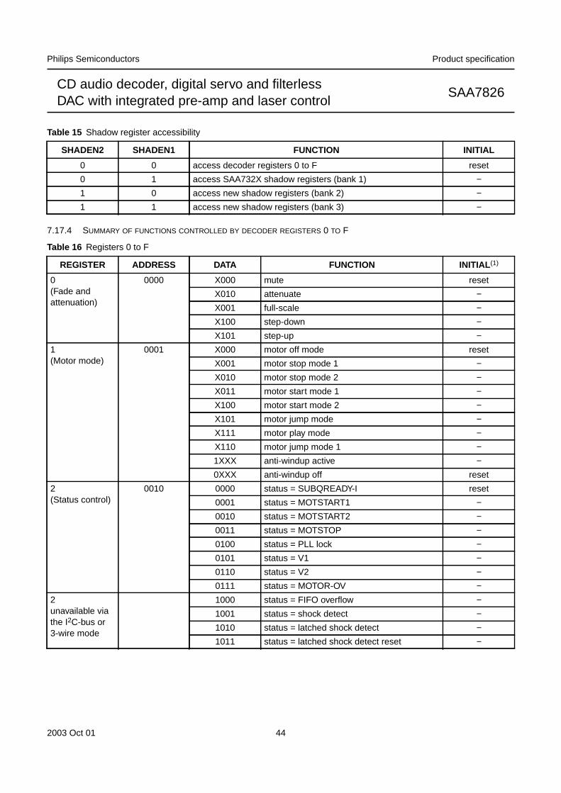
2003 Oct 01 44
Philips Semiconductors Product specification
CD audio decoder, digital servo and filterlessDAC with integrated pre-amp and laser control
SAA7826
Table 15 Shadow register accessibility
7.17.4 SUMMARY OF FUNCTIONS CONTROLLED BY DECODER REGISTERS 0 TO F
Table 16 Registers 0 to F
SHADEN2 SHADEN1 FUNCTION INITIAL
0 0 access decoder registers 0 to F reset
0 1 access SAA732X shadow registers (bank 1) −1 0 access new shadow registers (bank 2) −1 1 access new shadow registers (bank 3) −
REGISTER ADDRESS DATA FUNCTION INITIAL (1)
0(Fade andattenuation)
0000 X000 mute reset
X010 attenuate −X001 full-scale −X100 step-down −X101 step-up −
1(Motor mode)
0001 X000 motor off mode reset
X001 motor stop mode 1 −X010 motor stop mode 2 −X011 motor start mode 1 −X100 motor start mode 2 −X101 motor jump mode −X111 motor play mode −X110 motor jump mode 1 −1XXX anti-windup active −0XXX anti-windup off reset
2(Status control)
0010 0000 status = SUBQREADY-I reset
0001 status = MOTSTART1 −0010 status = MOTSTART2 −0011 status = MOTSTOP −0100 status = PLL lock −0101 status = V1 −0110 status = V2 −0111 status = MOTOR-OV −
2unavailable viathe I2C-bus or3-wire mode
1000 status = FIFO overflow −1001 status = shock detect −1010 status = latched shock detect −1011 status = latched shock detect reset −
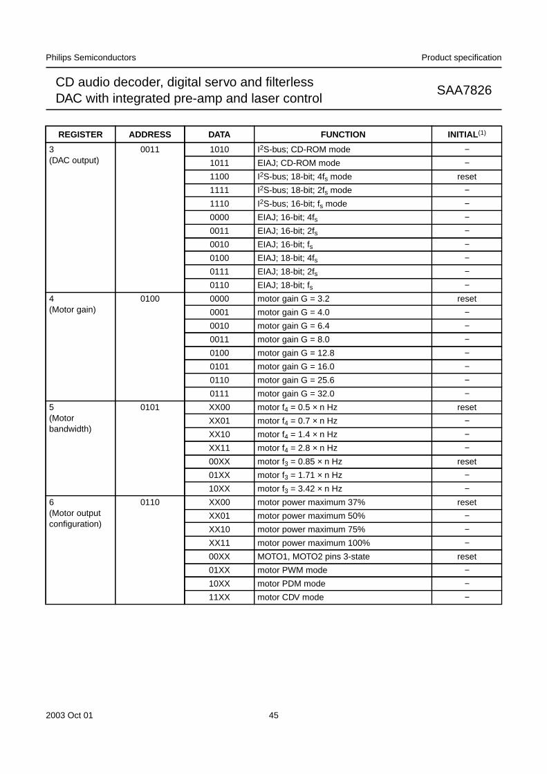
2003 Oct 01 45
Philips Semiconductors Product specification
CD audio decoder, digital servo and filterlessDAC with integrated pre-amp and laser control
SAA7826
3(DAC output)
0011 1010 I2S-bus; CD-ROM mode −1011 EIAJ; CD-ROM mode −1100 I2S-bus; 18-bit; 4fs mode reset
1111 I2S-bus; 18-bit; 2fs mode −1110 I2S-bus; 16-bit; fs mode −0000 EIAJ; 16-bit; 4fs −0011 EIAJ; 16-bit; 2fs −0010 EIAJ; 16-bit; fs −0100 EIAJ; 18-bit; 4fs −0111 EIAJ; 18-bit; 2fs −0110 EIAJ; 18-bit; fs −
4(Motor gain)
0100 0000 motor gain G = 3.2 reset
0001 motor gain G = 4.0 −0010 motor gain G = 6.4 −0011 motor gain G = 8.0 −0100 motor gain G = 12.8 −0101 motor gain G = 16.0 −0110 motor gain G = 25.6 −0111 motor gain G = 32.0 −
5(Motorbandwidth)
0101 XX00 motor f4 = 0.5 × n Hz reset
XX01 motor f4 = 0.7 × n Hz −XX10 motor f4 = 1.4 × n Hz −XX11 motor f4 = 2.8 × n Hz −00XX motor f3 = 0.85 × n Hz reset
01XX motor f3 = 1.71 × n Hz −10XX motor f3 = 3.42 × n Hz −
6(Motor outputconfiguration)
0110 XX00 motor power maximum 37% reset
XX01 motor power maximum 50% −XX10 motor power maximum 75% −XX11 motor power maximum 100% −00XX MOTO1, MOTO2 pins 3-state reset
01XX motor PWM mode −10XX motor PDM mode −11XX motor CDV mode −
REGISTER ADDRESS DATA FUNCTION INITIAL (1)
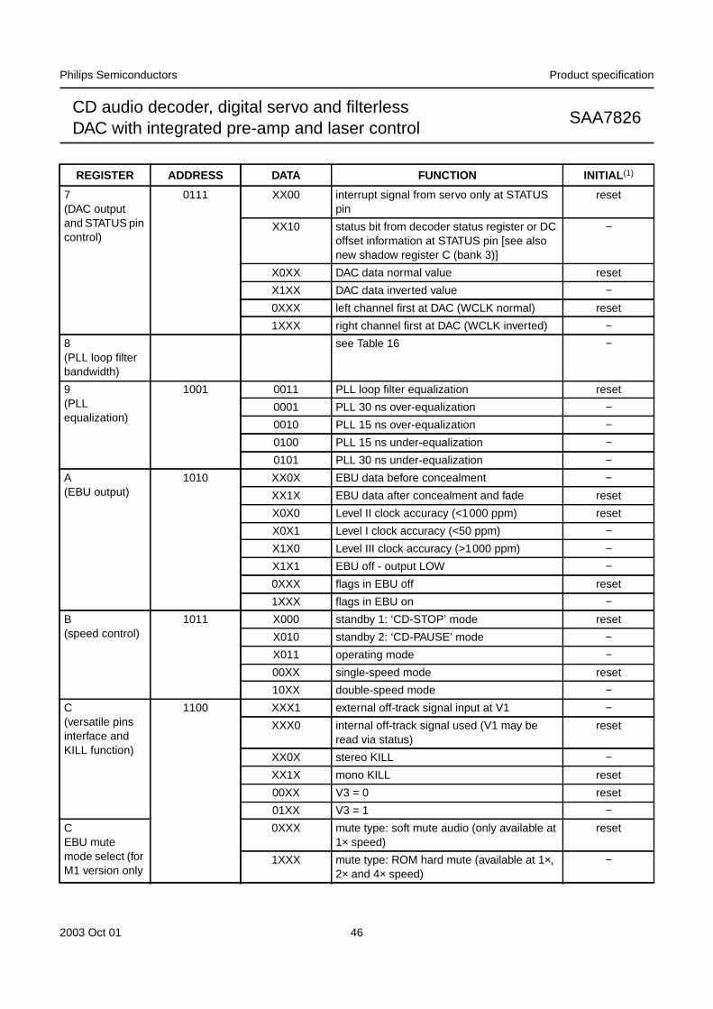
2003 Oct 01 46
Philips Semiconductors Product specification
CD audio decoder, digital servo and filterlessDAC with integrated pre-amp and laser control
SAA7826
7(DAC outputand STATUS pincontrol)
0111 XX00 interrupt signal from servo only at STATUSpin
reset
XX10 status bit from decoder status register or DCoffset information at STATUS pin [see alsonew shadow register C (bank 3)]
−
X0XX DAC data normal value reset
X1XX DAC data inverted value −0XXX left channel first at DAC (WCLK normal) reset
1XXX right channel first at DAC (WCLK inverted) −8(PLL loop filterbandwidth)
see Table 16 −
9(PLLequalization)
1001 0011 PLL loop filter equalization reset
0001 PLL 30 ns over-equalization −0010 PLL 15 ns over-equalization −0100 PLL 15 ns under-equalization −0101 PLL 30 ns under-equalization −
A(EBU output)
1010 XX0X EBU data before concealment −XX1X EBU data after concealment and fade reset
X0X0 Level II clock accuracy (<1000 ppm) reset
X0X1 Level I clock accuracy (<50 ppm) −X1X0 Level III clock accuracy (>1000 ppm) −X1X1 EBU off - output LOW −0XXX flags in EBU off reset
1XXX flags in EBU on −B(speed control)
1011 X000 standby 1: ‘CD-STOP’ mode reset
X010 standby 2: ‘CD-PAUSE’ mode −X011 operating mode −00XX single-speed mode reset
10XX double-speed mode −C(versatile pinsinterface andKILL function)
1100 XXX1 external off-track signal input at V1 −XXX0 internal off-track signal used (V1 may be
read via status)reset
XX0X stereo KILL −XX1X mono KILL reset
00XX V3 = 0 reset
01XX V3 = 1 −CEBU mutemode select (forM1 version only
0XXX mute type: soft mute audio (only available at1× speed)
reset
1XXX mute type: ROM hard mute (available at 1×,2× and 4× speed)
−
REGISTER ADDRESS DATA FUNCTION INITIAL (1)
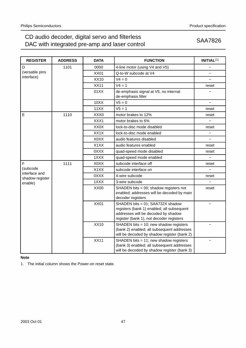
2003 Oct 01 47
Philips Semiconductors Product specification
CD audio decoder, digital servo and filterlessDAC with integrated pre-amp and laser control
SAA7826
Note
1. The initial column shows the Power-on reset state.
D(versatile pinsinterface)
1101 0000 4-line motor (using V4 and V5) −XX01 Q-to-W subcode at V4 −XX10 V4 = 0 −XX11 V4 = 1 reset
01XX de-emphasis signal at V5, no internalde-emphasis filter
−
10XX V5 = 0 −11XX V5 = 1 reset
E 1110 XXX0 motor brakes to 12% reset
XXX1 motor brakes to 6% −XX0X lock-to-disc mode disabled reset
XX1X lock-to-disc mode enabled −X0XX audio features disabled −X1XX audio features enabled reset
0XXX quad-speed mode disabled reset
1XXX quad-speed mode enabled −F(subcodeinterface andshadow registerenable)
1111 X0XX subcode interface off reset
X1XX subcode interface on −0XXX 4-wire subcode reset
1XXX 3-wire subcode −XX00 SHADEN bits = 00; shadow registers not
enabled; addresses will be decoded by maindecoder registers
reset
XX01 SHADEN bits = 01; SAA732X shadowregisters (bank 1) enabled; all subsequentaddresses will be decoded by shadowregister (bank 1), not decoder registers
−
XX10 SHADEN bits = 10; new shadow registers(bank 2) enabled; all subsequent addresseswill be decoded by shadow register (bank 2)
−
XX11 SHADEN bits = 11; new shadow registers(bank 3) enabled; all subsequent addresseswill be decoded by shadow register (bank 3)
−
REGISTER ADDRESS DATA FUNCTION INITIAL (1)
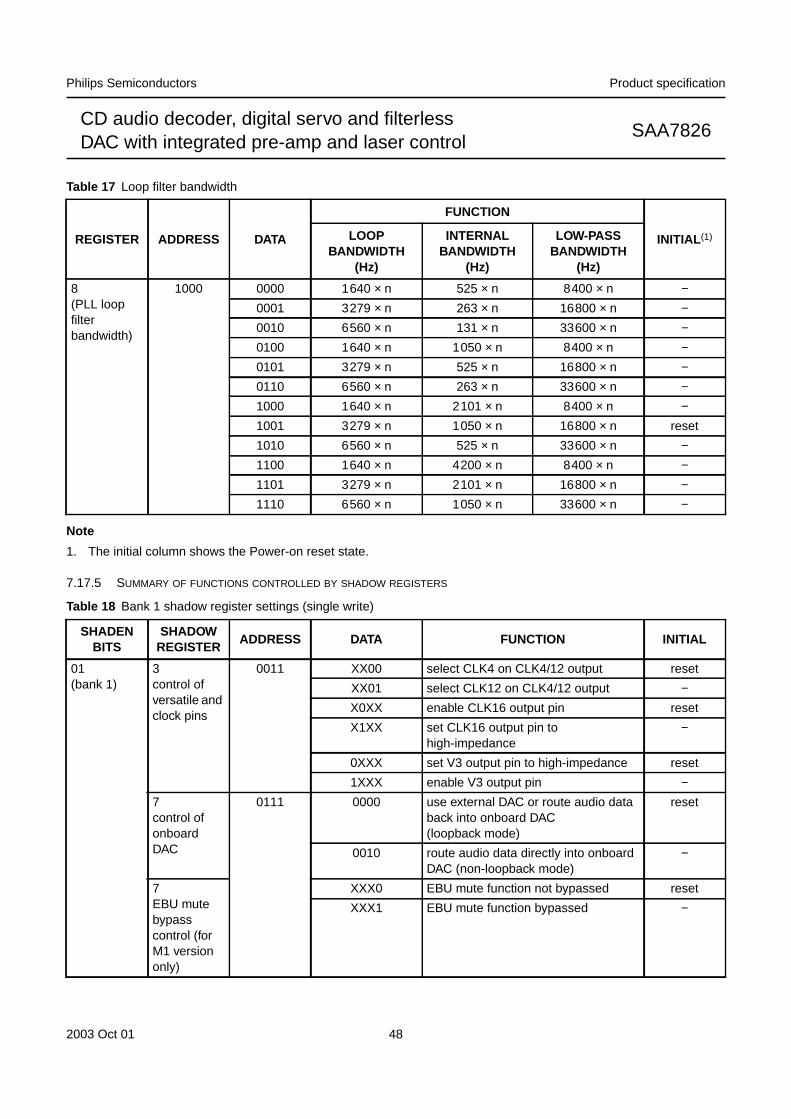
2003 Oct 01 48
Philips Semiconductors Product specification
CD audio decoder, digital servo and filterlessDAC with integrated pre-amp and laser control
SAA7826
Table 17 Loop filter bandwidth
Note
1. The initial column shows the Power-on reset state.
7.17.5 SUMMARY OF FUNCTIONS CONTROLLED BY SHADOW REGISTERS
Table 18 Bank 1 shadow register settings (single write)
REGISTER ADDRESS DATA
FUNCTION
INITIAL (1)LOOPBANDWIDTH
(Hz)
INTERNALBANDWIDTH
(Hz)
LOW-PASSBANDWIDTH
(Hz)
8(PLL loopfilterbandwidth)
1000 0000 1640 × n 525 × n 8400 × n −0001 3279 × n 263 × n 16800 × n −0010 6560 × n 131 × n 33600 × n −0100 1640 × n 1050 × n 8400 × n −0101 3279 × n 525 × n 16800 × n −0110 6560 × n 263 × n 33600 × n −1000 1640 × n 2101 × n 8400 × n −1001 3279 × n 1050 × n 16800 × n reset
1010 6560 × n 525 × n 33600 × n −1100 1640 × n 4200 × n 8400 × n −1101 3279 × n 2101 × n 16800 × n −1110 6560 × n 1050 × n 33600 × n −
SHADENBITS
SHADOWREGISTER
ADDRESS DATA FUNCTION INITIAL
01(bank 1)
3control ofversatile andclock pins
0011 XX00 select CLK4 on CLK4/12 output reset
XX01 select CLK12 on CLK4/12 output −X0XX enable CLK16 output pin reset
X1XX set CLK16 output pin tohigh-impedance
−
0XXX set V3 output pin to high-impedance reset
1XXX enable V3 output pin −7control ofonboardDAC
0111 0000 use external DAC or route audio databack into onboard DAC(loopback mode)
reset
0010 route audio data directly into onboardDAC (non-loopback mode)
−
7EBU mutebypasscontrol (forM1 versiononly)
XXX0 EBU mute function not bypassed reset
XXX1 EBU mute function bypassed −
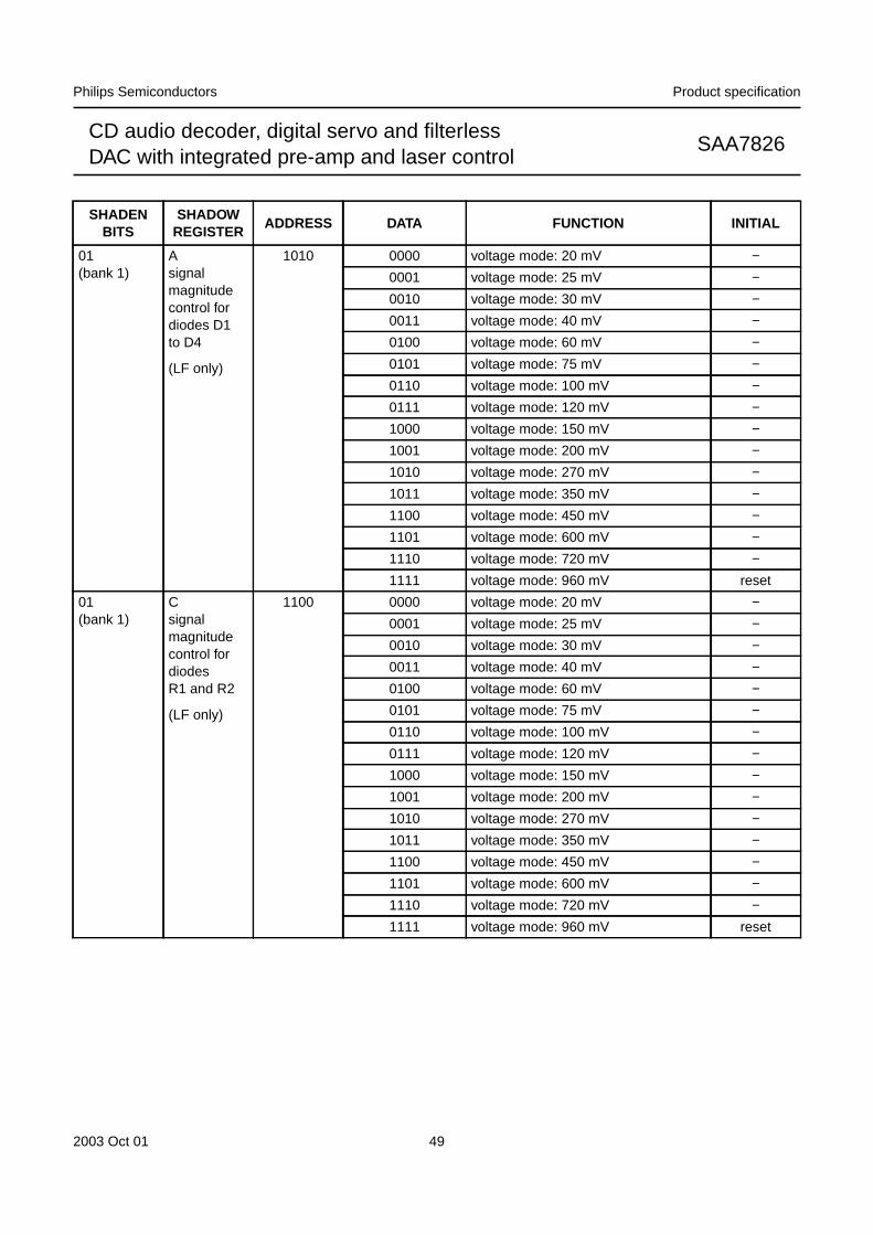
2003 Oct 01 49
Philips Semiconductors Product specification
CD audio decoder, digital servo and filterlessDAC with integrated pre-amp and laser control
SAA7826
01(bank 1)
Asignalmagnitudecontrol fordiodes D1to D4
(LF only)
1010 0000 voltage mode: 20 mV −0001 voltage mode: 25 mV −0010 voltage mode: 30 mV −0011 voltage mode: 40 mV −0100 voltage mode: 60 mV −0101 voltage mode: 75 mV −0110 voltage mode: 100 mV −0111 voltage mode: 120 mV −1000 voltage mode: 150 mV −1001 voltage mode: 200 mV −1010 voltage mode: 270 mV −1011 voltage mode: 350 mV −1100 voltage mode: 450 mV −1101 voltage mode: 600 mV −1110 voltage mode: 720 mV −1111 voltage mode: 960 mV reset
01(bank 1)
Csignalmagnitudecontrol fordiodesR1 and R2
(LF only)
1100 0000 voltage mode: 20 mV −0001 voltage mode: 25 mV −0010 voltage mode: 30 mV −0011 voltage mode: 40 mV −0100 voltage mode: 60 mV −0101 voltage mode: 75 mV −0110 voltage mode: 100 mV −0111 voltage mode: 120 mV −1000 voltage mode: 150 mV −1001 voltage mode: 200 mV −1010 voltage mode: 270 mV −1011 voltage mode: 350 mV −1100 voltage mode: 450 mV −1101 voltage mode: 600 mV −1110 voltage mode: 720 mV −1111 voltage mode: 960 mV reset
SHADENBITS
SHADOWREGISTER
ADDRESS DATA FUNCTION INITIAL
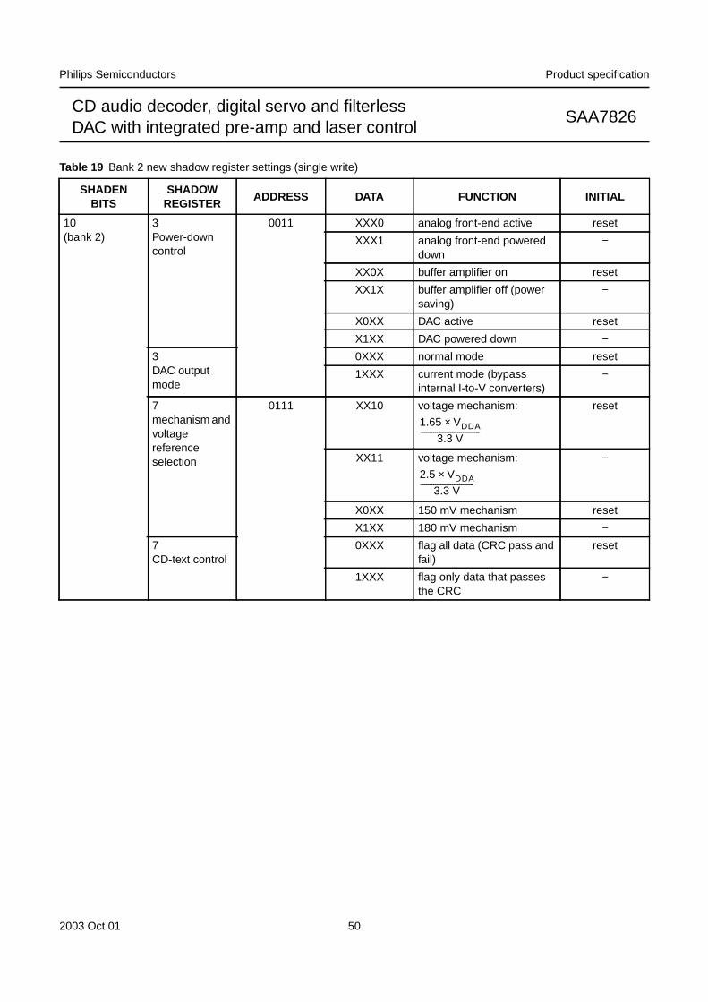
2003 Oct 01 50
Philips Semiconductors Product specification
CD audio decoder, digital servo and filterlessDAC with integrated pre-amp and laser control
SAA7826
Table 19 Bank 2 new shadow register settings (single write)
SHADENBITS
SHADOWREGISTER
ADDRESS DATA FUNCTION INITIAL
10(bank 2)
3Power-downcontrol
0011 XXX0 analog front-end active reset
XXX1 analog front-end powereddown
−
XX0X buffer amplifier on reset
XX1X buffer amplifier off (powersaving)
−
X0XX DAC active reset
X1XX DAC powered down −3DAC outputmode
0XXX normal mode reset
1XXX current mode (bypassinternal I-to-V converters)
−
7mechanism andvoltagereferenceselection
0111 XX10 voltage mechanism: reset
XX11 voltage mechanism: −
X0XX 150 mV mechanism reset
X1XX 180 mV mechanism −7CD-text control
0XXX flag all data (CRC pass andfail)
reset
1XXX flag only data that passesthe CRC
−
1.65 VDDA×3.3 V
--------------------------------
2.5 VDDA×3.3 V
-----------------------------
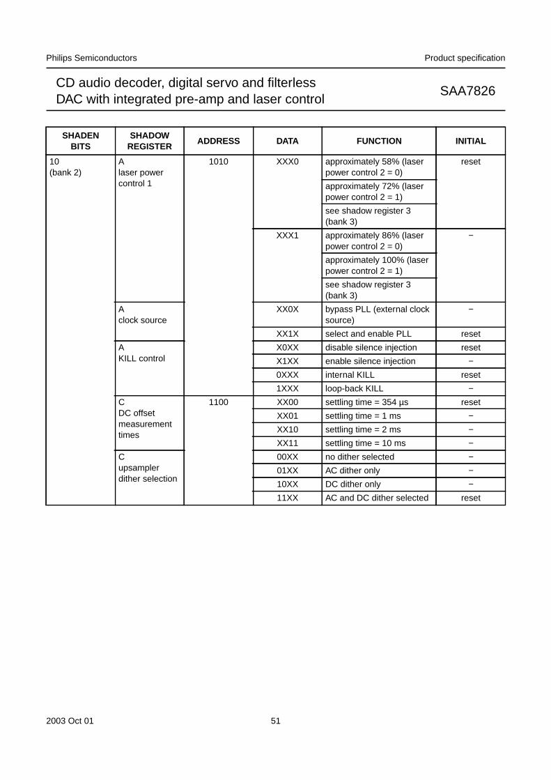
2003 Oct 01 51
Philips Semiconductors Product specification
CD audio decoder, digital servo and filterlessDAC with integrated pre-amp and laser control
SAA7826
10(bank 2)
Alaser powercontrol 1
1010 XXX0 approximately 58% (laserpower control 2 = 0)
reset
approximately 72% (laserpower control 2 = 1)
see shadow register 3(bank 3)
XXX1 approximately 86% (laserpower control 2 = 0)
−
approximately 100% (laserpower control 2 = 1)
see shadow register 3(bank 3)
Aclock source
XX0X bypass PLL (external clocksource)
−
XX1X select and enable PLL reset
AKILL control
X0XX disable silence injection reset
X1XX enable silence injection −0XXX internal KILL reset
1XXX loop-back KILL −CDC offsetmeasurementtimes
1100 XX00 settling time = 354 µs reset
XX01 settling time = 1 ms −XX10 settling time = 2 ms −XX11 settling time = 10 ms −
Cupsamplerdither selection
00XX no dither selected −01XX AC dither only −10XX DC dither only −11XX AC and DC dither selected reset
SHADENBITS
SHADOWREGISTER
ADDRESS DATA FUNCTION INITIAL
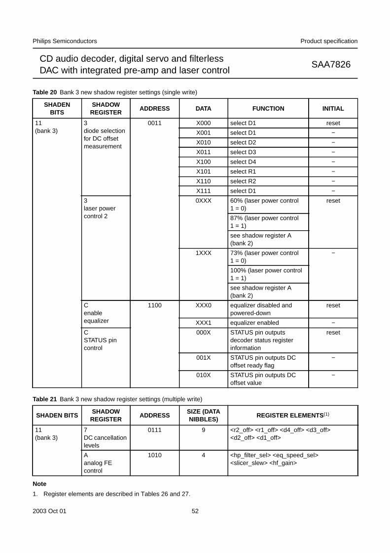
2003 Oct 01 52
Philips Semiconductors Product specification
CD audio decoder, digital servo and filterlessDAC with integrated pre-amp and laser control
SAA7826
Table 20 Bank 3 new shadow register settings (single write)
Table 21 Bank 3 new shadow register settings (multiple write)
Note
1. Register elements are described in Tables 26 and 27.
SHADENBITS
SHADOWREGISTER
ADDRESS DATA FUNCTION INITIAL
11(bank 3)
3diode selectionfor DC offsetmeasurement
0011 X000 select D1 reset
X001 select D1 −X010 select D2 −X011 select D3 −X100 select D4 −X101 select R1 −X110 select R2 −X111 select D1 −
3laser powercontrol 2
0XXX 60% (laser power control1 = 0)
reset
87% (laser power control1 = 1)
see shadow register A(bank 2)
1XXX 73% (laser power control1 = 0)
−
100% (laser power control1 = 1)
see shadow register A(bank 2)
Cenableequalizer
1100 XXX0 equalizer disabled andpowered-down
reset
XXX1 equalizer enabled −CSTATUS pincontrol
000X STATUS pin outputsdecoder status registerinformation
reset
001X STATUS pin outputs DCoffset ready flag
−
010X STATUS pin outputs DCoffset value
−
SHADEN BITSSHADOW
REGISTERADDRESS
SIZE (DATANIBBLES)
REGISTER ELEMENTS(1)
11(bank 3)
7DC cancellationlevels
0111 9 <r2_off> <r1_off> <d4_off> <d3_off><d2_off> <d1_off>
Aanalog FEcontrol
1010 4 <hp_filter_sel> <eq_speed_sel><slicer_slew> <hf_gain>
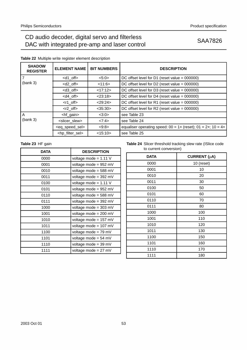
2003 Oct 01 53
Philips Semiconductors Product specification
CD audio decoder, digital servo and filterlessDAC with integrated pre-amp and laser control
SAA7826
Table 22 Multiple write register element description
SHADOWREGISTER
ELEMENT NAME BIT NUMBERS DESCRIPTION
7(bank 3)
<d1_off> <5:0> DC offset level for D1 (reset value = 000000)
<d2_off> <11:6> DC offset level for D2 (reset value = 000000)
<d3_off> <17:12> DC offset level for D3 (reset value = 000000)
<d4_off> <23:18> DC offset level for D4 (reset value = 000000)
<r1_off> <29:24> DC offset level for R1 (reset value = 000000)
<r2_off> <35:30> DC offset level for R2 (reset value = 000000)
A(bank 3)
<hf_gain> <3:0> see Table 23
<slicer_slew> <7:4> see Table 24
<eq_speed_sel> <9:8> equaliser operating speed: 00 = 1× (reset); 01 = 2×; 10 = 4×<hp_filter_sel> <15:10> see Table 25
Table 23 HF gain Table 24 Slicer threshold tracking slew rate (ISlice codeto current conversion)
DATA DESCRIPTION
0000 voltage mode = 1.11 V
0001 voltage mode = 952 mV
0010 voltage mode = 588 mV
0011 voltage mode = 392 mV
0100 voltage mode = 1.11 V
0101 voltage mode = 952 mV
0110 voltage mode = 588 mV
0111 voltage mode = 392 mV
1000 voltage mode = 303 mV
1001 voltage mode = 200 mV
1010 voltage mode = 157 mV
1011 voltage mode = 107 mV
1100 voltage mode = 79 mV
1101 voltage mode = 54 mV
1110 voltage mode = 39 mV
1111 voltage mode = 27 mV
DATA CURRENT (µA)
0000 10 (reset)
0001 10
0010 20
0011 30
0100 50
0101 60
0110 70
0111 80
1000 100
1001 110
1010 120
1011 130
1100 150
1101 160
1110 170
1111 180
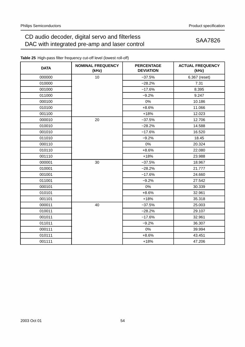
2003 Oct 01 54
Philips Semiconductors Product specification
CD audio decoder, digital servo and filterlessDAC with integrated pre-amp and laser control
SAA7826
Table 25 High-pass filter frequency cut-off level (lowest roll-off)
DATANOMINAL FREQUENCY
(kHz)PERCENTAGE
DEVIATIONACTUAL FREQUENCY
(kHz)
000000 10 −37.5% 6.367 (reset)
010000 −28.2% 7.31
001000 −17.6% 8.395
011000 −9.2% 9.247
000100 0% 10.186
010100 +8.6% 11.066
001100 +18% 12.023
000010 20 −37.5% 12.706
010010 −28.2% 14.588
001010 −17.6% 16.520
011010 −9.2% 18.45
000110 0% 20.324
010110 +8.6% 22.080
001110 +18% 23.988
000001 30 −37.5% 18.967
010001 −28.2% 21.777
001001 −17.6% 24.660
011001 −9.2% 27.542
000101 0% 30.339
010101 +8.6% 32.961
001101 +18% 35.318
000011 40 −37.5% 25.003
010011 −28.2% 29.107
001011 −17.6% 32.961
011011 −9.2% 36.307
000111 0% 39.994
010111 +8.6% 43.451
001111 +18% 47.206
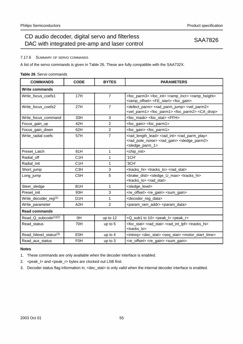
2003 Oct 01 55
Philips Semiconductors Product specification
CD audio decoder, digital servo and filterlessDAC with integrated pre-amp and laser control
SAA7826
7.17.6 SUMMARY OF SERVO COMMANDS
A list of the servo commands is given in Table 26. These are fully compatible with the SAA732X.
Table 26 Servo commands
Notes
1. These commands are only available when the decoder interface is enabled.
2. <peak_I> and <peak_r> bytes are clocked out LSB first.
3. Decoder status flag information in, <dec_stat> is only valid when the internal decoder interface is enabled.
COMMANDS CODE BYTES PARAMETERS
Write commands
Write_focus_coefs1 17H 7 <foc_parm3> <foc_int> <ramp_incr> <ramp_height><ramp_offset> <FE_start> <foc_gain>
Write_focus_coefs2 27H 7 <defect_parm> <rad_parm_jump> <vel_parm2><vel_parm1> <foc_parm1> <foc_parm2> <CA_drop>
Write_focus_command 33H 3 <foc_mask> <foc_stat> <FFH>
Focus_gain_up 42H 2 <foc_gain> <foc_parm1>
Focus_gain_down 62H 2 <foc_gain> <foc_parm1>
Write_radial coefs 57H 7 <rad_length_lead> <rad_int> <rad_parm_play><rad_pole_noise> <rad_gain> <sledge_parm2><sledge_parm_1>
Preset_Latch 81H 1 <chip_init>
Radial_off C1H 1 ‘1CH’
Radial_init C1H 1 ‘3CH’
Short_jump C3H 3 <tracks_hi> <tracks_lo> <rad_stat>
Long_jump C5H 5 <brake_dist> <sledge_U_max> <tracks_hi><tracks_lo> <rad_stat>
Steer_sledge B1H 1 <sledge_level>
Preset_init 93H 3 <re_offset> <re_gain> <sum_gain>
Write_decoder_reg(1) D1H 1 <decoder_reg_data>
Write_parameter A2H 2 <param_ram_addr> <param_data>
Read commands
Read_Q_subcode(1)(2) 0H up to 12 <Q_sub1 to 10> <peak_l> <peak_r>
Read_status 70H up to 5 <foc_stat> <rad_stat> <rad_int_lpf> <tracks_hi><tracks_lo>
Read_hilevel_status(3) E0H up to 4 <intreq> <dec_stat> <seq_stat> <motor_start_time>
Read_aux_status F0H up to 3 <re_offset> <re_gain> <sum_gain>
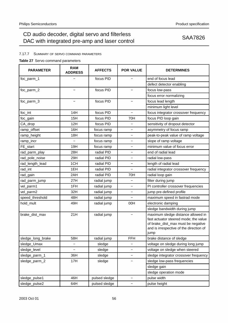
2003 Oct 01 56
Philips Semiconductors Product specification
CD audio decoder, digital servo and filterlessDAC with integrated pre-amp and laser control
SAA7826
7.17.7 SUMMARY OF SERVO COMMAND PARAMETERS
Table 27 Servo command parameters
PARAMETERRAM
ADDRESSAFFECTS POR VALUE DETERMINES
foc_parm_1 − focus PID − end of focus lead
defect detector enabling
foc_parm_2 − focus PID − focus low-pass
focus error normalizing
foc_parm_3 − focus PID − focus lead length
minimum light level
foc_int 14H focus PID − focus integrator crossover frequency
foc_gain 15H focus PID 70H focus PID loop gain
CA_drop 12H focus PID − sensitivity of dropout detector
ramp_offset 16H focus ramp − asymmetry of focus ramp
ramp_height 18H focus ramp − peak-to-peak value of ramp voltage
ramp_incr − focus ramp − slope of ramp voltage
FE_start 19H focus ramp − minimum value of focus error
rad_parm_play 28H radial PID − end of radial lead
rad_pole_noise 29H radial PID − radial low-pass
rad_length_lead 1CH radial PID − length of radial lead
rad_int 1EH radial PID − radial integrator crossover frequency
rad_gain 2AH radial PID 70H radial loop gain
rad_parm_jump 27H radial jump − filter during jump
vel_parm1 1FH radial jump − PI controller crossover frequencies
vel_parm2 32H radial jump − jump pre-defined profile
speed_threshold 48H radial jump − maximum speed in fastrad mode
hold_mult 49H radial jump 00H electronic damping
sledge bandwidth during jump
brake_dist_max 21H radial jump − maximum sledge distance allowed infast actuator steered mode; the valueof brake_dist_max must be negativeand is irrespective of the direction ofjump
sledge_long_brake 58H radial jump FFH brake distance of sledge
sledge_Umax − sledge − voltage on sledge during long jump
sledge_level − sledge − voltage on sledge when steered
sledge_parm_1 36H sledge − sledge integrator crossover frequency
sledge_parm_2 17H sledge − sledge low-pass frequencies
sledge gain
sledge operation mode
sledge_pulse1 46H pulsed sledge − pulse width
sledge_pulse2 64H pulsed sledge − pulse height
2003 Oct 01 57
Philips Semiconductors Product specification
CD audio decoder, digital servo and filterlessDAC with integrated pre-amp and laser control
SAA7826
defect_parm − defect detector − defect detector setting
playwatchtime 54H Watchdog − radial on-track Watchdog time
jumpwatchtime 57H Watchdog − radial jump Watchdog time-out
radcontrol 59H Watchdog − enable/disable automatic radial offfeature
chip_init − set-up − enable/disable decoder interface
xtra_preset 4AH set-up 38H laser on/off
RA, FO and SL PDM modulatingfrequency
fast jumping circuit on/off
cd6cmd 4DH decoderinterface
− decoder part commands
interrupt_mask 53H STATUS pin − enabled interrupts
seq_control 42H autosequencer − autosequencer control
focus_start_time 5EH autosequencer − focus start time
motor_start_time1 5FH autosequencer − motor start 1 time
motor_start_time2 60H autosequencer − motor start 2 time
radial_init_time 61H autosequencer − radial initialization time
brake_time 62H autosequencer − brake time
RadCmdByte 63H autosequencer − radial command byte
osc_inc 68H focus/radialAGC
− AGC control
− frequency of injected signal
phase_shift 67H focus/radialAGC
− phase shift of injected signal
level1 69H focus/radialAGC
− amplitude of signal injected
level2 6AH focus/radialAGC
− amplitude of signal injected
agc_gain 6CH focus/radialAGC
− focus/radial gain
PARAMETERRAM
ADDRESSAFFECTS POR VALUE DETERMINES
2003 Oct 01 58
Philips Semiconductors Product specification
CD audio decoder, digital servo and filterlessDAC with integrated pre-amp and laser control
SAA7826
8 SUMMARY OF SERVO COMMAND PARAMETERSVALUES
Table 28 foc_parm1 parameter: focus end leadfrequency, defect detector, offtrack detector
Table 29 foc_parm2 parameter: focus low-pass startfrequency, focusing system
foc_parm1Focus end lead
frequency f 3 kHzfoc_pole_lead value(binary)
xxx1 1100 1.97
xxx1 1000 2.29
xxx0 0000 2.61
xxx0 1000 2.94
xxx0 1100 3.26
xxx1 1101 3.90
xxx1 1001 4.55
xxx0 0001 5.19
xxx0 1001 5.82
xxx0 1101 6.46
xxx1 1110 7.72
xxx1 1010 8.98
xxx0 0010 10.22
xxx0 1010 11.46
xxx0 1110 12.69
xxx1 1111 15.13
xxx1 1011 17.54
xxx0 0011 19.93
xxx0 1011 22.28
defect_det_sw Defect detector
x11x xxxx defect detector does notinfluence focus and radial
x10x xxxx focus hold on defectdetector
x00x xxxx focus and radial hold ondefect detector
x01x xxxx undefined, reserved
otd_select Offtrack detector
0xxx xxxx ON track active 1
1xxx xxxx ON track active 0
foc_parm2Focus low-pass start
frequency f 4 kHzfoc_pole_noise value(binary)
xxx1 1100 3.90
xxx1 1000 4.55
xxx0 0000 5.19
xxx0 1000 5.82
xxx0 1100 6.46
xxx1 1101 7.72
xxx1 1001 8.98
xxx0 0001 10.22
xxx0 1001 11.46
xxx0 1101 12.69
xxx1 1110 15.13
xxx1 1010 17.54
xxx0 0010 19.93
xxx0 1010 22.28
xxx0 1110 25.40
xxx1 1111 30.26
xxx1 1011 35.08
xxx0 0011 39.86
xxx0 1011 44.56
detector_arr Focusing system
xx1x xxxx single foucault
xx0x xxxx double foucault
2003 Oct 01 59
Philips Semiconductors Product specification
CD audio decoder, digital servo and filterlessDAC with integrated pre-amp and laser control
SAA7826
Table 30 foc_parm3 parameter: focus lead length, CAstart level for focus acquisition
Table 31 CA_drop parameter: CA level for dropoutdetection
Table 32 FE_start parameter: minimum threshold forfocus start
Table 33 foc_int_strength parameter: focus integratorstrength
Table 34 foc_gain parameter: focus gain
foc_parm3
Focus lead length f 3/f2foc_lead_length value(binary)
0000 xxx1 64
1000 xxx1 32
0100 xxx1 21.3
1100 xxx1 16
0010 xxx1 12.8
1010 xxx1 10.7
0110 xxx1 9.1
1110 xxx1 8
0001 xxx1 7.1
1001 xxx1 6.4
0101 xxx1 5.8
1101 xxx1 5.3
0011 xxx1 4.9
1011 xxx1 4.6
0111 xxx1 4.3
1111 xxx1 4
CA_start value (binary) CA min
xxxx 000x 0.0225
xxxx 001x 0.03
xxxx 010x 0.045
xxxx 011x 0.06
xxxx 100x 0.09
xxxx 101x 0.125
xxxx 110x 0.18
xxxx 111x 1.0
CA_drop value (binary) CA min
xxx0 0000 0.0225
xxx0 0100 0.03
xxx0 1000 0.045
xxx0 1100 0.06
xxx1 0000 0.09
xxx1 0100 0.125
xxx1 1000 0.18
xxx1 1100 1.0
FE_start value (decimal)Minimum threshold for
(d1 − d2)/(d1 + d2)
0 always
1 1/127
2 2/127
i i/127
64 64/127
65...127 65 to 127/127
127 continuous ramping
128...255 not allowed
foc_int_strength value(decimal)
Focus integratorstrength f 5 Hz
0 integrator hold
1 1.2
2 2.4
i 1.2 × i
21 25
22...255 undefined
foc_gain value (decimal) G
1 2048
2 1024
3 2048/3
i 2048/i
255 2048/255
0 undefined
2003 Oct 01 60
Philips Semiconductors Product specification
CD audio decoder, digital servo and filterlessDAC with integrated pre-amp and laser control
SAA7826
Table 35 rad_pole_noise parameter: radial low-pass startfrequency
Table 36 rad_lead_length parameter: radial lead length
rad_pole_noise value(binary)
Radial low-pass startfrequency f 4 kHz
1101 1100 3.90
1011 1000 4.55
1010 0000 5.19
1010 1000 5.82
1000 1100 6.46
1001 1101 7.72
1001 1001 8.98
0100 0001 10.22
0100 1001 11.46
0100 1101 12.69
0101 1110 15.13
0101 1010 17.54
0100 0010 19.93
0100 1010 22.28
xxx0 1110 25.40
xxx1 1111 30.26
xxx1 1011 35.08
xxx0 0011 39.86
xxx0 1011 44.56
rad_lead_lengthvalue (binary)
rad_lead_lengthvalue (hex)
Radial leadlength f 3/f2
0000 xxxx 0x 128
1000 xxxx 8x 64
0100 xxxx 4x 42.7
1100 xxxx Cx 32
0010 xxxx 2x 25.6
1010 xxxx Ax 21.3
0110 xxxx 6x 18.3
1110 xxxx Ex 16
0001 xxxx 1x 14.2
1001 xxxx 9x 12.8
0101 xxxx 5x 11.6
1101 xxxx Dx 10.7
0011 xxxx 3x 9.8
1011 xxxx Bx 9.1
0111 xxxx 7x 8.5
1111 xxxx Fx 8
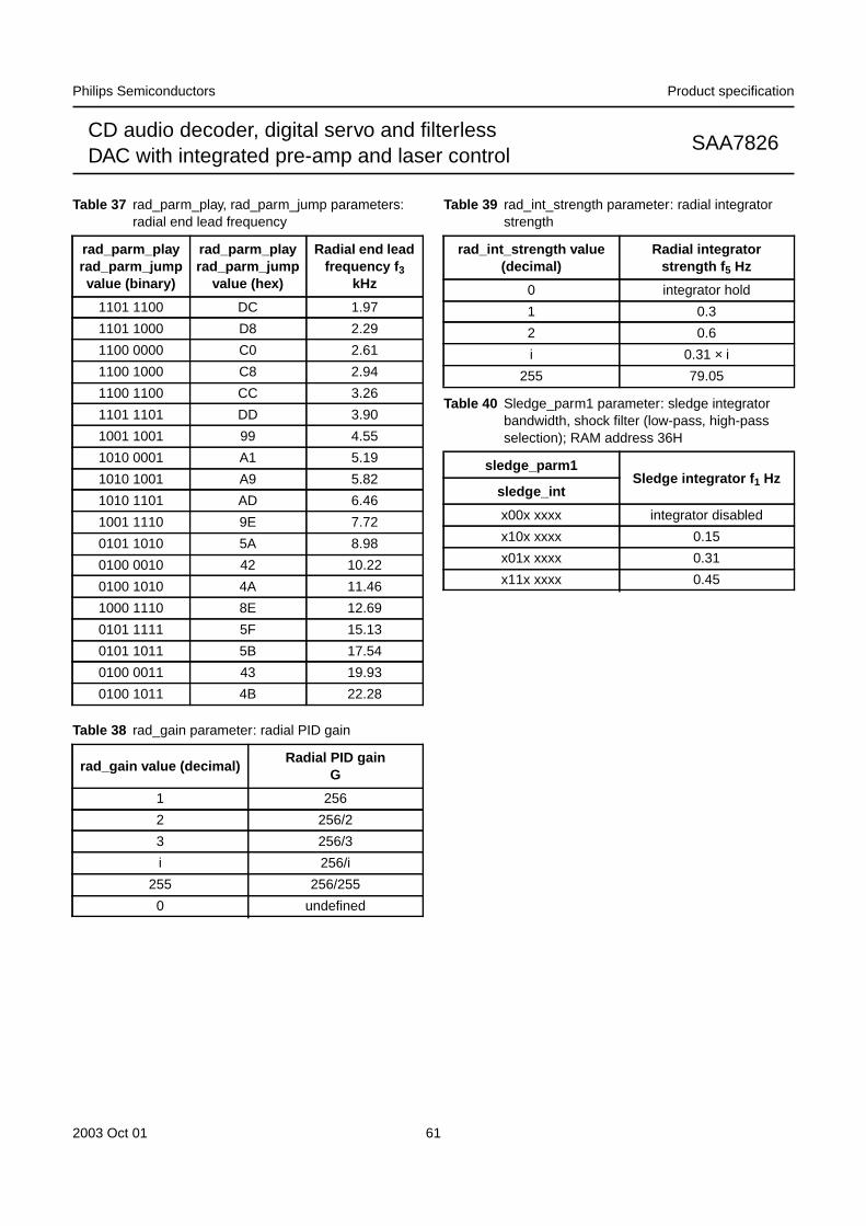
2003 Oct 01 61
Philips Semiconductors Product specification
CD audio decoder, digital servo and filterlessDAC with integrated pre-amp and laser control
SAA7826
Table 37 rad_parm_play, rad_parm_jump parameters:radial end lead frequency
Table 38 rad_gain parameter: radial PID gain
Table 39 rad_int_strength parameter: radial integratorstrength
Table 40 Sledge_parm1 parameter: sledge integratorbandwidth, shock filter (low-pass, high-passselection); RAM address 36H
rad_parm_playrad_parm_jumpvalue (binary)
rad_parm_playrad_parm_jump
value (hex)
Radial end leadfrequency f 3
kHz
1101 1100 DC 1.97
1101 1000 D8 2.29
1100 0000 C0 2.61
1100 1000 C8 2.94
1100 1100 CC 3.26
1101 1101 DD 3.90
1001 1001 99 4.55
1010 0001 A1 5.19
1010 1001 A9 5.82
1010 1101 AD 6.46
1001 1110 9E 7.72
0101 1010 5A 8.98
0100 0010 42 10.22
0100 1010 4A 11.46
1000 1110 8E 12.69
0101 1111 5F 15.13
0101 1011 5B 17.54
0100 0011 43 19.93
0100 1011 4B 22.28
rad_gain value (decimal)Radial PID gain
G
1 256
2 256/2
3 256/3
i 256/i
255 256/255
0 undefined
rad_int_strength value(decimal)
Radial integratorstrength f 5 Hz
0 integrator hold
1 0.3
2 0.6
i 0.31 × i
255 79.05
sledge_parm1Sledge integrator f 1 Hz
sledge_int
x00x xxxx integrator disabled
x10x xxxx 0.15
x01x xxxx 0.31
x11x xxxx 0.45
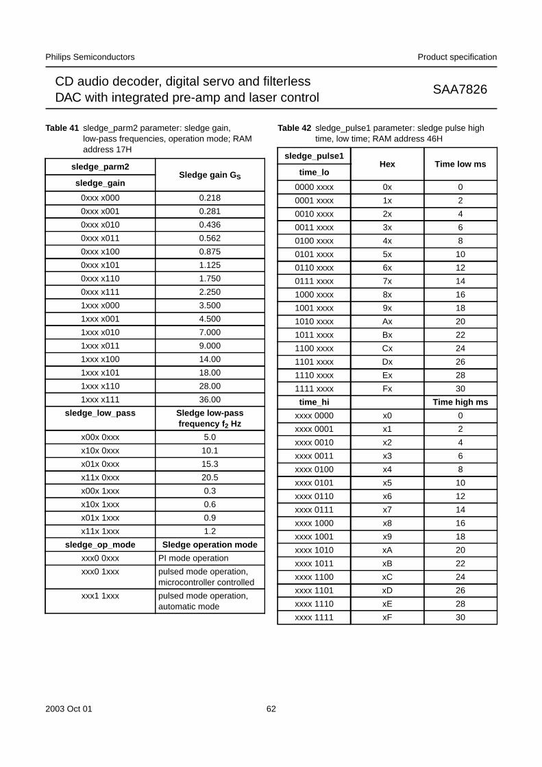
2003 Oct 01 62
Philips Semiconductors Product specification
CD audio decoder, digital servo and filterlessDAC with integrated pre-amp and laser control
SAA7826
Table 41 sledge_parm2 parameter: sledge gain,low-pass frequencies, operation mode; RAMaddress 17H
Table 42 sledge_pulse1 parameter: sledge pulse hightime, low time; RAM address 46H
sledge_parm2Sledge gain G S
sledge_gain
0xxx x000 0.218
0xxx x001 0.281
0xxx x010 0.436
0xxx x011 0.562
0xxx x100 0.875
0xxx x101 1.125
0xxx x110 1.750
0xxx x111 2.250
1xxx x000 3.500
1xxx x001 4.500
1xxx x010 7.000
1xxx x011 9.000
1xxx x100 14.00
1xxx x101 18.00
1xxx x110 28.00
1xxx x111 36.00
sledge_low_pass Sledge low-passfrequency f 2 Hz
x00x 0xxx 5.0
x10x 0xxx 10.1
x01x 0xxx 15.3
x11x 0xxx 20.5
x00x 1xxx 0.3
x10x 1xxx 0.6
x01x 1xxx 0.9
x11x 1xxx 1.2
sledge_op_mode Sledge operation mode
xxx0 0xxx PI mode operation
xxx0 1xxx pulsed mode operation,microcontroller controlled
xxx1 1xxx pulsed mode operation,automatic mode
sledge_pulse1Hex Time low ms
time_lo
0000 xxxx 0x 0
0001 xxxx 1x 2
0010 xxxx 2x 4
0011 xxxx 3x 6
0100 xxxx 4x 8
0101 xxxx 5x 10
0110 xxxx 6x 12
0111 xxxx 7x 14
1000 xxxx 8x 16
1001 xxxx 9x 18
1010 xxxx Ax 20
1011 xxxx Bx 22
1100 xxxx Cx 24
1101 xxxx Dx 26
1110 xxxx Ex 28
1111 xxxx Fx 30
time_hi Time high ms
xxxx 0000 x0 0
xxxx 0001 x1 2
xxxx 0010 x2 4
xxxx 0011 x3 6
xxxx 0100 x4 8
xxxx 0101 x5 10
xxxx 0110 x6 12
xxxx 0111 x7 14
xxxx 1000 x8 16
xxxx 1001 x9 18
xxxx 1010 xA 20
xxxx 1011 xB 22
xxxx 1100 xC 24
xxxx 1101 xD 26
xxxx 1110 xE 28
xxxx 1111 xF 30
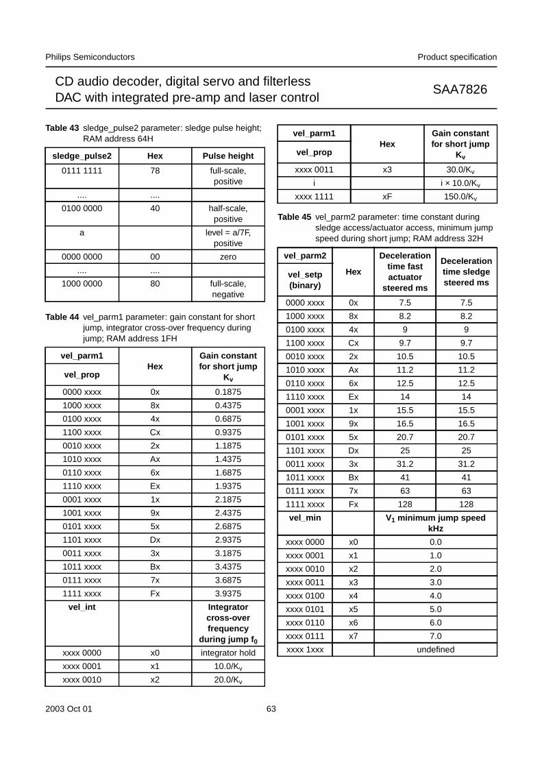
2003 Oct 01 63
Philips Semiconductors Product specification
CD audio decoder, digital servo and filterlessDAC with integrated pre-amp and laser control
SAA7826
Table 43 sledge_pulse2 parameter: sledge pulse height;RAM address 64H
Table 44 vel_parm1 parameter: gain constant for shortjump, integrator cross-over frequency duringjump; RAM address 1FH
Table 45 vel_parm2 parameter: time constant duringsledge access/actuator access, minimum jumpspeed during short jump; RAM address 32H
sledge_pulse2 Hex Pulse height
0111 1111 78 full-scale,positive
.... ....
0100 0000 40 half-scale,positive
a level = a/7F,positive
0000 0000 00 zero
.... ....
1000 0000 80 full-scale,negative
vel_parm1Hex
Gain constantfor short jump
Kvvel_prop
0000 xxxx 0x 0.1875
1000 xxxx 8x 0.4375
0100 xxxx 4x 0.6875
1100 xxxx Cx 0.9375
0010 xxxx 2x 1.1875
1010 xxxx Ax 1.4375
0110 xxxx 6x 1.6875
1110 xxxx Ex 1.9375
0001 xxxx 1x 2.1875
1001 xxxx 9x 2.4375
0101 xxxx 5x 2.6875
1101 xxxx Dx 2.9375
0011 xxxx 3x 3.1875
1011 xxxx Bx 3.4375
0111 xxxx 7x 3.6875
1111 xxxx Fx 3.9375
vel_int Integratorcross-overfrequency
during jump f 0
xxxx 0000 x0 integrator hold
xxxx 0001 x1 10.0/Kv
xxxx 0010 x2 20.0/Kv
xxxx 0011 x3 30.0/Kv
i i × 10.0/Kv
xxxx 1111 xF 150.0/Kv
vel_parm2
Hex
Decelerationtime fastactuator
steered ms
Decelerationtime sledgesteered ms
vel_setp(binary)
0000 xxxx 0x 7.5 7.5
1000 xxxx 8x 8.2 8.2
0100 xxxx 4x 9 9
1100 xxxx Cx 9.7 9.7
0010 xxxx 2x 10.5 10.5
1010 xxxx Ax 11.2 11.2
0110 xxxx 6x 12.5 12.5
1110 xxxx Ex 14 14
0001 xxxx 1x 15.5 15.5
1001 xxxx 9x 16.5 16.5
0101 xxxx 5x 20.7 20.7
1101 xxxx Dx 25 25
0011 xxxx 3x 31.2 31.2
1011 xxxx Bx 41 41
0111 xxxx 7x 63 63
1111 xxxx Fx 128 128
vel_min V 1 minimum jump speedkHz
xxxx 0000 x0 0.0
xxxx 0001 x1 1.0
xxxx 0010 x2 2.0
xxxx 0011 x3 3.0
xxxx 0100 x4 4.0
xxxx 0101 x5 5.0
xxxx 0110 x6 6.0
xxxx 0111 x7 7.0
xxxx 1xxx undefined
vel_parm1Hex
Gain constantfor short jump
Kvvel_prop
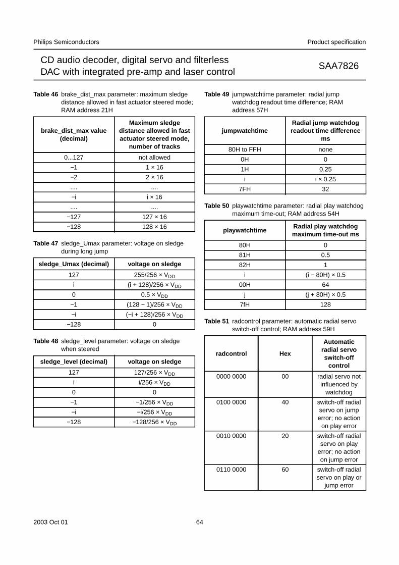
2003 Oct 01 64
Philips Semiconductors Product specification
CD audio decoder, digital servo and filterlessDAC with integrated pre-amp and laser control
SAA7826
Table 46 brake_dist_max parameter: maximum sledgedistance allowed in fast actuator steered mode;RAM address 21H
Table 47 sledge_Umax parameter: voltage on sledgeduring long jump
Table 48 sledge_level parameter: voltage on sledgewhen steered
Table 49 jumpwatchtime parameter: radial jumpwatchdog readout time difference; RAMaddress 57H
Table 50 playwatchtime parameter: radial play watchdogmaximum time-out; RAM address 54H
Table 51 radcontrol parameter: automatic radial servoswitch-off control; RAM address 59H
brake_dist_max value(decimal)
Maximum sledgedistance allowed in fastactuator steered mode,
number of tracks
0...127 not allowed
−1 1 × 16
−2 2 × 16
.... ....
−i i × 16
.... ....
−127 127 × 16
−128 128 × 16
sledge_Umax (decimal) voltage on sledge
127 255/256 × VDD
i (i + 128)/256 × VDD
0 0.5 × VDD
−1 (128 − 1)/256 × VDD
−i (−i + 128)/256 × VDD
−128 0
sledge_level (decimal) voltage on sledge
127 127/256 × VDD
i i/256 × VDD
0 0
−1 −1/256 × VDD
−i −i/256 × VDD
−128 −128/256 × VDD
jumpwatchtimeRadial jump watchdogreadout time difference
ms
80H to FFH none
0H 0
1H 0.25
i i × 0.25
7FH 32
playwatchtimeRadial play watchdogmaximum time-out ms
80H 0
81H 0.5
82H 1
i (i − 80H) × 0.5
00H 64
j (j + 80H) × 0.5
7fH 128
radcontrol Hex
Automaticradial servoswitch-off
control
0000 0000 00 radial servo notinfluenced by
watchdog
0100 0000 40 switch-off radialservo on jumperror; no action
on play error
0010 0000 20 switch-off radialservo on play
error; no actionon jump error
0110 0000 60 switch-off radialservo on play or
jump error
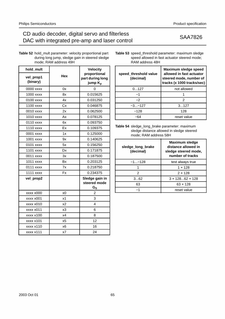
2003 Oct 01 65
Philips Semiconductors Product specification
CD audio decoder, digital servo and filterlessDAC with integrated pre-amp and laser control
SAA7826
Table 52 hold_mult parameter: velocity proportional partduring long jump, sledge gain in steered sledgemode; RAM address 49H
Table 53 speed_threshold parameter: maximum sledgespeed allowed in fast actuator steered mode;RAM address 48H
Table 54 sledge_long_brake parameter: maximumsledge distance allowed in sledge steeredmode; RAM address 58H
hold_mult
Hex
Velocityproportional
part during longjump K p
vel_prop1(binary)
0000 xxxx 0x 0
1000 xxxx 8x 0.015625
0100 xxxx 4x 0.031250
1100 xxxx Cx 0.046875
0010 xxxx 2x 0.062500
1010 xxxx Ax 0.078125
0110 xxxx 6x 0.093750
1110 xxxx Ex 0.109375
0001 xxxx 1x 0.125000
1001 xxxx 9x 0.140625
0101 xxxx 5x 0.156250
1101 xxxx Dx 0.171875
0011 xxxx 3x 0.187500
1011 xxxx Bx 0.203125
0111 xxxx 7x 0.218750
1111 xxxx Fx 0.234375
vel_prop2 Sledge gain insteered mode
GS
xxxx x000 x0 2
xxxx x001 x1 3
xxxx x010 x2 4
xxxx x011 x3 6
xxxx x100 x4 8
xxxx x101 x5 12
xxxx x110 x6 16
xxxx x111 x7 24
speed_threshold value(decimal)
Maximum sledge speedallowed in fast actuator
steered mode, number oftracks (x 1000 tracks/sec)
0...127 not allowed
−1 1
−2 2
−3...−127 3...127
−128 128
−64 reset value
sledge_long_brake(decimal)
Maximum sledgedistance allowed in
sledge steered mode,number of tracks
−1...−128 test always true
1 1 × 128
2 2 × 128
3...62 3 × 128...62 × 128
63 63 × 128
−1 reset value
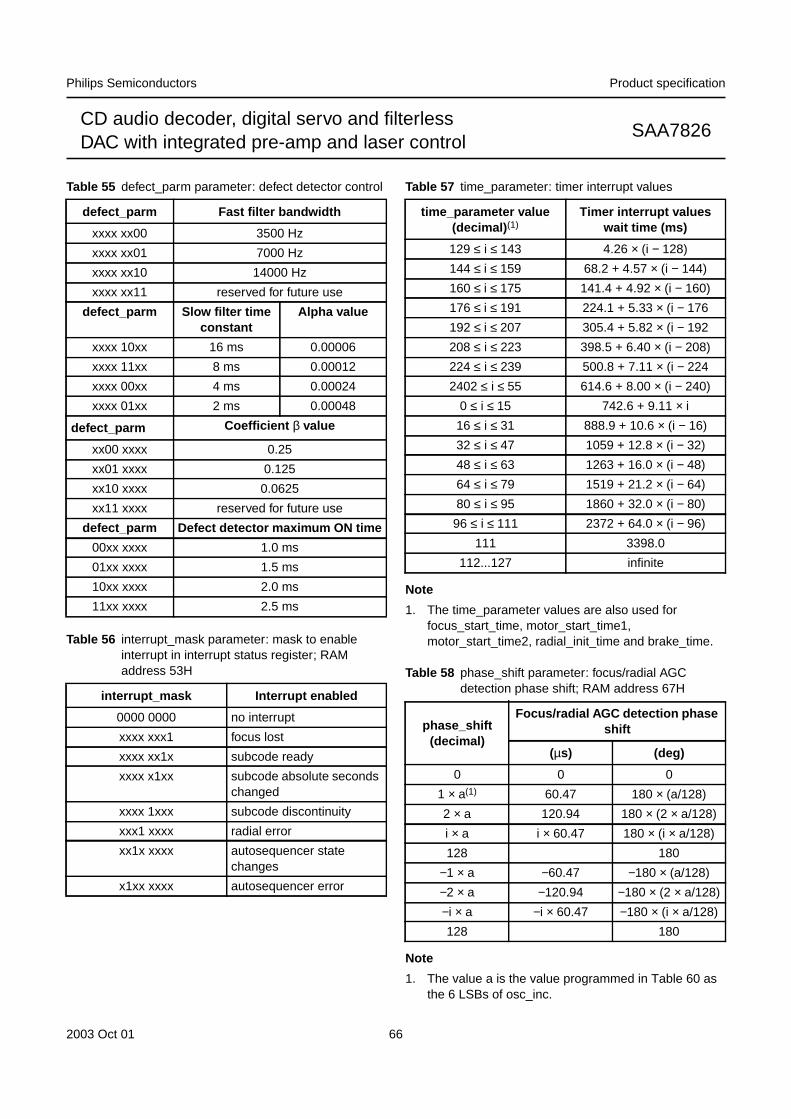
2003 Oct 01 66
Philips Semiconductors Product specification
CD audio decoder, digital servo and filterlessDAC with integrated pre-amp and laser control
SAA7826
Table 55 defect_parm parameter: defect detector control
Table 56 interrupt_mask parameter: mask to enableinterrupt in interrupt status register; RAMaddress 53H
Table 57 time_parameter: timer interrupt values
Note
1. The time_parameter values are also used forfocus_start_time, motor_start_time1,motor_start_time2, radial_init_time and brake_time.
Table 58 phase_shift parameter: focus/radial AGCdetection phase shift; RAM address 67H
Note
1. The value a is the value programmed in Table 60 asthe 6 LSBs of osc_inc.
defect_parm Fast filter bandwidth
xxxx xx00 3500 Hz
xxxx xx01 7000 Hz
xxxx xx10 14000 Hz
xxxx xx11 reserved for future use
defect_parm Slow filter timeconstant
Alpha value
xxxx 10xx 16 ms 0.00006
xxxx 11xx 8 ms 0.00012
xxxx 00xx 4 ms 0.00024
xxxx 01xx 2 ms 0.00048
defect_parm Coefficient β value
xx00 xxxx 0.25
xx01 xxxx 0.125
xx10 xxxx 0.0625
xx11 xxxx reserved for future use
defect_parm Defect detector maximum ON time
00xx xxxx 1.0 ms
01xx xxxx 1.5 ms
10xx xxxx 2.0 ms
11xx xxxx 2.5 ms
interrupt_mask Interrupt enabled
0000 0000 no interrupt
xxxx xxx1 focus lost
xxxx xx1x subcode ready
xxxx x1xx subcode absolute secondschanged
xxxx 1xxx subcode discontinuity
xxx1 xxxx radial error
xx1x xxxx autosequencer statechanges
x1xx xxxx autosequencer error
time_parameter value(decimal) (1)
Timer interrupt valueswait time (ms)
129 ≤ i ≤ 143 4.26 × (i − 128)
144 ≤ i ≤ 159 68.2 + 4.57 × (i − 144)
160 ≤ i ≤ 175 141.4 + 4.92 × (i − 160)
176 ≤ i ≤ 191 224.1 + 5.33 × (i − 176
192 ≤ i ≤ 207 305.4 + 5.82 × (i − 192
208 ≤ i ≤ 223 398.5 + 6.40 × (i − 208)
224 ≤ i ≤ 239 500.8 + 7.11 × (i − 224
2402 ≤ i ≤ 55 614.6 + 8.00 × (i − 240)
0 ≤ i ≤ 15 742.6 + 9.11 × i
16 ≤ i ≤ 31 888.9 + 10.6 × (i − 16)
32 ≤ i ≤ 47 1059 + 12.8 × (i − 32)
48 ≤ i ≤ 63 1263 + 16.0 × (i − 48)
64 ≤ i ≤ 79 1519 + 21.2 × (i − 64)
80 ≤ i ≤ 95 1860 + 32.0 × (i − 80)
96 ≤ i ≤ 111 2372 + 64.0 × (i − 96)
111 3398.0
112...127 infinite
phase_shift(decimal)
Focus/radial AGC detection phaseshift
(µs) (deg)
0 0 0
1 × a(1) 60.47 180 × (a/128)
2 × a 120.94 180 × (2 × a/128)
i × a i × 60.47 180 × (i × a/128)
128 180
−1 × a −60.47 −180 × (a/128)
−2 × a −120.94 −180 × (2 × a/128)
−i × a −i × 60.47 −180 × (i × a/128)
128 180
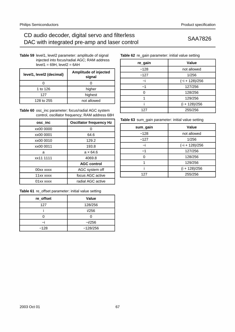
2003 Oct 01 67
Philips Semiconductors Product specification
CD audio decoder, digital servo and filterlessDAC with integrated pre-amp and laser control
SAA7826
Table 59 level1, level2 parameter: amplitude of signalinjected into focus/radial AGC; RAM addresslevel1 = 69H, level2 = 6AH
Table 60 osc_inc parameter: focus/radial AGC systemcontrol, oscillator frequency; RAM address 68H
Table 61 re_offset parameter: initial value setting
Table 62 re_gain parameter: initial value setting
Table 63 sum_gain parameter: initial value setting
level1, level2 (decimal)Amplitude of injected
signal
0 0
1 to 126 higher
127 highest
128 to 255 not allowed
osc_inc Oscillator frequency Hz
xx00 0000 0
xx00 0001 64.6
xx00 0010 129.2
xx00 0011 193.8
a a × 64.6
xx11 1111 4069.8
AGC control
00xx xxxx AGC system off
11xx xxxx focus AGC active
01xx xxxx radial AGC active
re_offset Value
127 128/256
i i/256
0 0
−i −i/256
−128 −128/256
re_gain Value
−128 not allowed
−127 1/256
−i (−i + 128)/256
−1 127/256
0 128/256
1 129/256
i (i + 128)/256
127 255/256
sum_gain Value
−128 not allowed
−127 1/256
−i (−i + 128)/256
−1 127/256
0 128/256
1 129/256
i (i + 128)/256
127 255/256
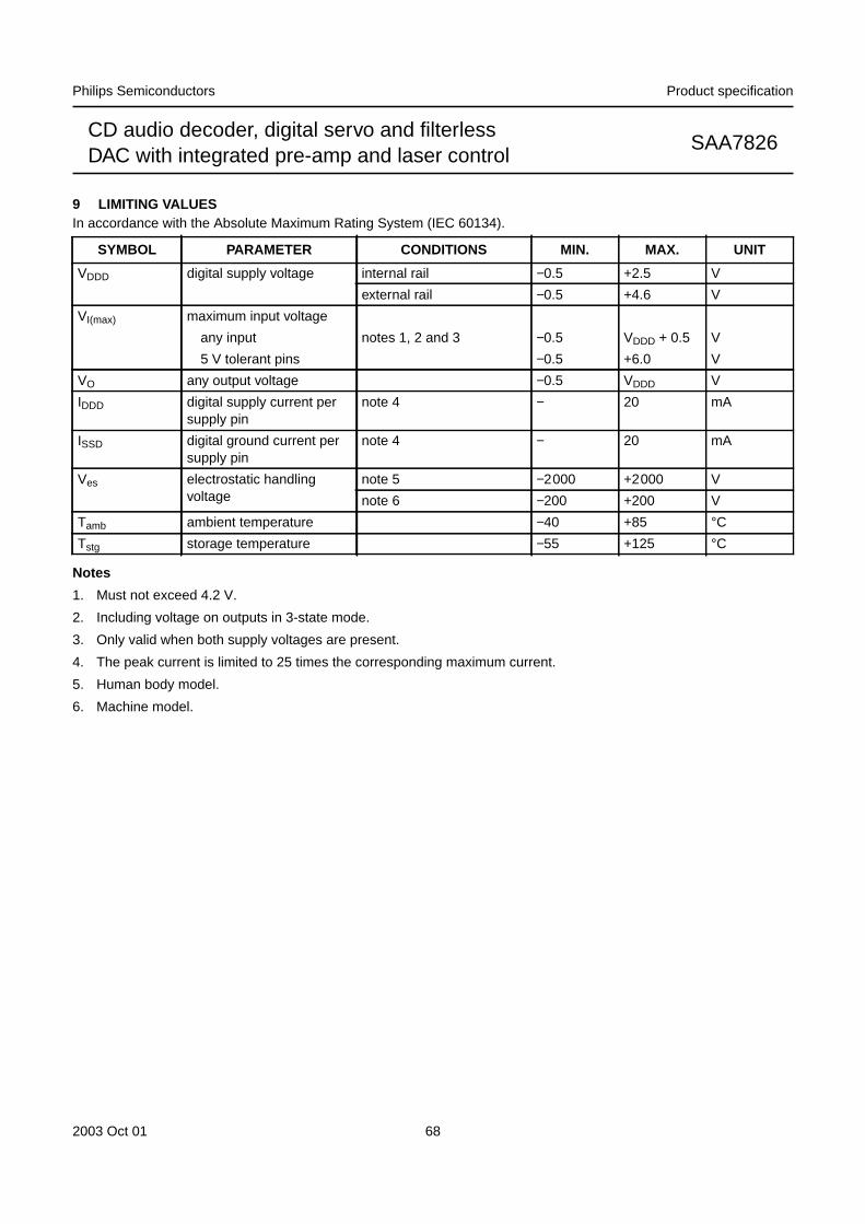
2003 Oct 01 68
Philips Semiconductors Product specification
CD audio decoder, digital servo and filterlessDAC with integrated pre-amp and laser control
SAA7826
9 LIMITING VALUESIn accordance with the Absolute Maximum Rating System (IEC 60134).
Notes
1. Must not exceed 4.2 V.
2. Including voltage on outputs in 3-state mode.
3. Only valid when both supply voltages are present.
4. The peak current is limited to 25 times the corresponding maximum current.
5. Human body model.
6. Machine model.
SYMBOL PARAMETER CONDITIONS MIN. MAX. UNIT
VDDD digital supply voltage internal rail −0.5 +2.5 V
external rail −0.5 +4.6 V
VI(max) maximum input voltage
any input notes 1, 2 and 3 −0.5 VDDD + 0.5 V
5 V tolerant pins −0.5 +6.0 V
VO any output voltage −0.5 VDDD V
IDDD digital supply current persupply pin
note 4 − 20 mA
ISSD digital ground current persupply pin
note 4 − 20 mA
Ves electrostatic handlingvoltage
note 5 −2000 +2000 V
note 6 −200 +200 V
Tamb ambient temperature −40 +85 °CTstg storage temperature −55 +125 °C
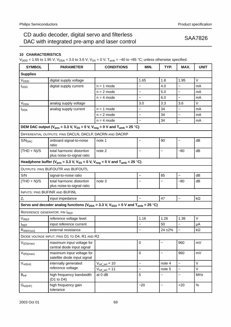
2003 Oct 01 69
Philips Semiconductors Product specification
CD audio decoder, digital servo and filterlessDAC with integrated pre-amp and laser control
SAA7826
10 CHARACTERISTICSVDDD = 1.65 to 1.95 V; VDDA = 3.0 to 3.6 V; VSS = 0 V; Tamb = −40 to +85 °C; unless otherwise specified.
SYMBOL PARAMETER CONDITIONS MIN. TYP. MAX. UNIT
Supplies
VDDD digital supply voltage 1.65 1.8 1.95 V
IDDD digital supply current n = 1 mode − 4.0 − mA
n = 2 mode − 5.0 − mA
n = 4 mode − 6.0 − mA
VDDA analog supply voltage 3.0 3.3 3.6 V
IDDA analog supply current n = 1 mode − 34 − mA
n = 2 mode − 34 − mA
n = 4 mode − 34 − mA
DEM DAC output (V pos = 3.3 V, VSS = 0 V, Vneg = 0 V and Tamb = 25 °C)
DIFFERENTIAL OUTPUTS: PINS DACLN, DACLP, DACRN AND DACRP
S/NDAC onboard signal-to-noiseratio
note 1 − 90 − dB
(THD + N)/S total harmonic distortionplus noise-to-signal ratio
note 2 − − −80 dB
Headphone buffer (V pos = 3.3 V, VSS = 0 V, Vneg = 0 V and Tamb = 25 °C)
OUTPUTS: PINS BUFOUTR AND BUFOUTL
S/N signal-to-noise ratio − 85 − dB
(THD + N)/S total harmonic distortionplus noise-to-signal ratio
note 3 − − −80 dB
INPUTS: PINS BUFINR AND BUFINL
Zi input impedance − 47 − kΩ
Servo and decoder analog functions (V DDA = 3.3 V, VSSA = 0 V and Tamb = 25 °C)
REFERENCE GENERATOR: PIN IREF
VIREF reference voltage level 1.16 1.26 1.36 V
IREF input reference current − 50 − µA
RIREF(ext) external resistance − 24 ±2% − kΩ
DIODE VOLTAGE INPUT: PINS D1 TO D4, R1 AND R2
Vi(D)(max) maximum input voltage forcentral diode input signal
0 − 960 mV
Vi(R)(max) maximum input voltage forsatellite diode input signal
0 − 960 mV
Vref(int) internally generatedreference voltage
Vref_sel = 10 − note 4 − V
Vref_sel = 11 − note 5 − V
BHF high frequency bandwidth(D1 to D4)
at 0 dB 5 − − MHz
Gtol(HF) high frequency gaintolerance
−20 − +20 %
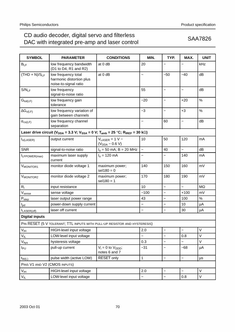
2003 Oct 01 70
Philips Semiconductors Product specification
CD audio decoder, digital servo and filterlessDAC with integrated pre-amp and laser control
SAA7826
BLF low frequency bandwidth(D1 to D4, R1 and R2)
at 0 dB 20 − − kHz
(THD + N)/SLF low frequency totalharmonic distortion plusnoise-to-signal ratio
at 0 dB − −50 −40 dB
S/NLF low frequencysignal-to-noise ratio
55 − − dB
Gtol(LF) low frequency gaintolerance
−20 − +20 %
∆Gv(LF) low frequency variation ofgain between channels
−3 − +3 %
αcs(LF) low frequency channelseparation
− 60 − dB
Laser drive circuit (V DDA = 3.3 V; VSSA = 0 V; Tamb = 25 °C; RIREF = 30 kΩ)
Io(LASER) output current VLASER = 1 V −(VDDA − 0.6 V)
10 50 120 mA
SNR signal-to-noise ratio Io = 50 mA; B = 20 MHz − 40 − dB
ILFPOWER(max) maximum laser supplycurrent
Io = 120 mA − − 140 mA
VMONITOR1 monitor diode voltage 1 maximum power;sel180 = 0
140 150 160 mV
VMONITOR2 monitor diode voltage 2 maximum power;sel180 = 1
170 180 190 mV
Ri input resistance 10 − − MΩVsense sense voltage −100 − +100 mV
Pstep laser output power range 43 − 100 %
Ipd power-down supply current − − 10 µA
ILASER(off) laser off current − − 30 µA
Digital inputs
PIN RESET (5 V TOLERANT; TTL INPUTS WITH PULL-UP RESISTOR AND HYSTERESIS)
VIH HIGH-level input voltage 2.0 − − V
VIL LOW-level input voltage − − 0.8 V
Vhys hysteresis voltage 0.3 − − V
IPU pull-up current Vi = 0 to VDDD;notes 6 and 7
−31 − −68 µA
tW(L) pulse width (active LOW) RESET only 1 − − µs
PINS V1 AND V2 (CMOS INPUTS)
VIH HIGH-level input voltage 2.0 − − V
VIL LOW-level input voltage − − 0.8 V
SYMBOL PARAMETER CONDITIONS MIN. TYP. MAX. UNIT
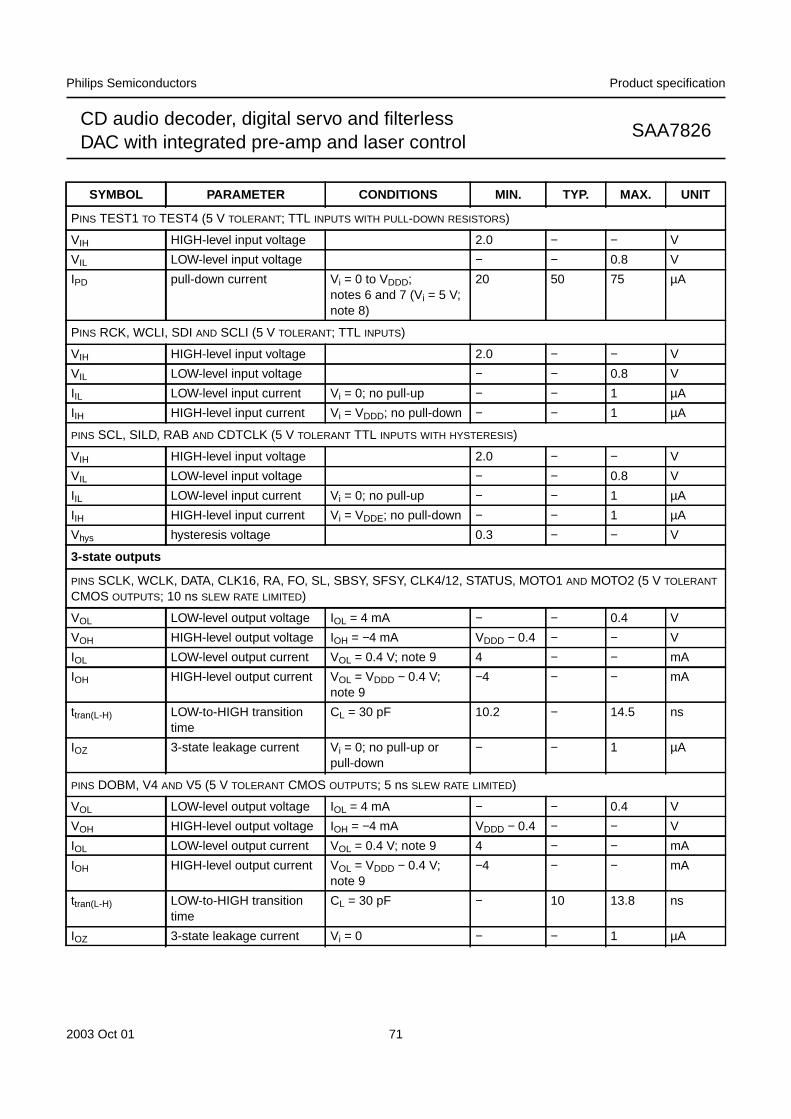
2003 Oct 01 71
Philips Semiconductors Product specification
CD audio decoder, digital servo and filterlessDAC with integrated pre-amp and laser control
SAA7826
PINS TEST1 TO TEST4 (5 V TOLERANT; TTL INPUTS WITH PULL-DOWN RESISTORS)
VIH HIGH-level input voltage 2.0 − − V
VIL LOW-level input voltage − − 0.8 V
IPD pull-down current Vi = 0 to VDDD;notes 6 and 7 (Vi = 5 V;note 8)
20 50 75 µA
PINS RCK, WCLI, SDI AND SCLI (5 V TOLERANT; TTL INPUTS)
VIH HIGH-level input voltage 2.0 − − V
VIL LOW-level input voltage − − 0.8 V
IIL LOW-level input current Vi = 0; no pull-up − − 1 µA
IIH HIGH-level input current Vi = VDDD; no pull-down − − 1 µA
PINS SCL, SILD, RAB AND CDTCLK (5 V TOLERANT TTL INPUTS WITH HYSTERESIS)
VIH HIGH-level input voltage 2.0 − − V
VIL LOW-level input voltage − − 0.8 V
IIL LOW-level input current Vi = 0; no pull-up − − 1 µA
IIH HIGH-level input current Vi = VDDE; no pull-down − − 1 µA
Vhys hysteresis voltage 0.3 − − V
3-state outputs
PINS SCLK, WCLK, DATA, CLK16, RA, FO, SL, SBSY, SFSY, CLK4/12, STATUS, MOTO1 AND MOTO2 (5 V TOLERANT
CMOS OUTPUTS; 10 ns SLEW RATE LIMITED)
VOL LOW-level output voltage IOL = 4 mA − − 0.4 V
VOH HIGH-level output voltage IOH = −4 mA VDDD − 0.4 − − V
IOL LOW-level output current VOL = 0.4 V; note 9 4 − − mA
IOH HIGH-level output current VOL = VDDD − 0.4 V;note 9
−4 − − mA
ttran(L-H) LOW-to-HIGH transitiontime
CL = 30 pF 10.2 − 14.5 ns
IOZ 3-state leakage current Vi = 0; no pull-up orpull-down
− − 1 µA
PINS DOBM, V4 AND V5 (5 V TOLERANT CMOS OUTPUTS; 5 ns SLEW RATE LIMITED)
VOL LOW-level output voltage IOL = 4 mA − − 0.4 V
VOH HIGH-level output voltage IOH = −4 mA VDDD − 0.4 − − V
IOL LOW-level output current VOL = 0.4 V; note 9 4 − − mA
IOH HIGH-level output current VOL = VDDD − 0.4 V;note 9
−4 − − mA
ttran(L-H) LOW-to-HIGH transitiontime
CL = 30 pF − 10 13.8 ns
IOZ 3-state leakage current Vi = 0 − − 1 µA
SYMBOL PARAMETER CONDITIONS MIN. TYP. MAX. UNIT
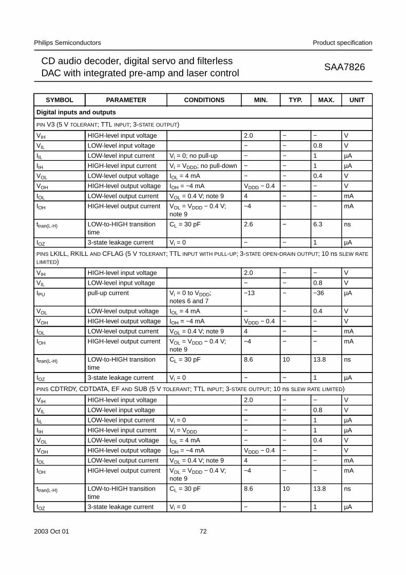
2003 Oct 01 72
Philips Semiconductors Product specification
CD audio decoder, digital servo and filterlessDAC with integrated pre-amp and laser control
SAA7826
Digital inputs and outputs
PIN V3 (5 V TOLERANT; TTL INPUT; 3-STATE OUTPUT)
VIH HIGH-level input voltage 2.0 − − V
VIL LOW-level input voltage − − 0.8 V
IIL LOW-level input current Vi = 0; no pull-up − − 1 µA
IIH HIGH-level input current Vi = VDDD; no pull-down − − 1 µA
VOL LOW-level output voltage IOL = 4 mA − − 0.4 V
VOH HIGH-level output voltage IOH = −4 mA VDDD − 0.4 − − V
IOL LOW-level output current VOL = 0.4 V; note 9 4 − − mA
IOH HIGH-level output current VOL = VDDD − 0.4 V;note 9
−4 − − mA
ttran(L-H) LOW-to-HIGH transitiontime
CL = 30 pF 2.6 − 6.3 ns
IOZ 3-state leakage current Vi = 0 − − 1 µA
PINS LKILL, RKILL AND CFLAG (5 V TOLERANT; TTL INPUT WITH PULL-UP; 3-STATE OPEN-DRAIN OUTPUT; 10 ns SLEW RATE
LIMITED)
VIH HIGH-level input voltage 2.0 − − V
VIL LOW-level input voltage − − 0.8 V
IPU pull-up current Vi = 0 to VDDD;notes 6 and 7
−13 − −36 µA
VOL LOW-level output voltage IOL = 4 mA − − 0.4 V
VOH HIGH-level output voltage IOH = −4 mA VDDD − 0.4 − − V
IOL LOW-level output current VOL = 0.4 V; note 9 4 − − mA
IOH HIGH-level output current VOL = VDDD − 0.4 V;note 9
−4 − − mA
ttran(L-H) LOW-to-HIGH transitiontime
CL = 30 pF 8.6 10 13.8 ns
IOZ 3-state leakage current Vi = 0 − − 1 µA
PINS CDTRDY, CDTDATA, EF AND SUB (5 V TOLERANT; TTL INPUT; 3-STATE OUTPUT; 10 ns SLEW RATE LIMITED)
VIH HIGH-level input voltage 2.0 − − V
VIL LOW-level input voltage − − 0.8 V
IIL LOW-level input current Vi = 0 − − 1 µA
IIH HIGH-level input current Vi = VDDD − − 1 µA
VOL LOW-level output voltage IOL = 4 mA − − 0.4 V
VOH HIGH-level output voltage IOH = −4 mA VDDD − 0.4 − − V
IOL LOW-level output current VOL = 0.4 V; note 9 4 − − mA
IOH HIGH-level output current VOL = VDDD − 0.4 V;note 9
−4 − − mA
ttran(L-H) LOW-to-HIGH transitiontime
CL = 30 pF 8.6 10 13.8 ns
IOZ 3-state leakage current Vi = 0 − − 1 µA
SYMBOL PARAMETER CONDITIONS MIN. TYP. MAX. UNIT
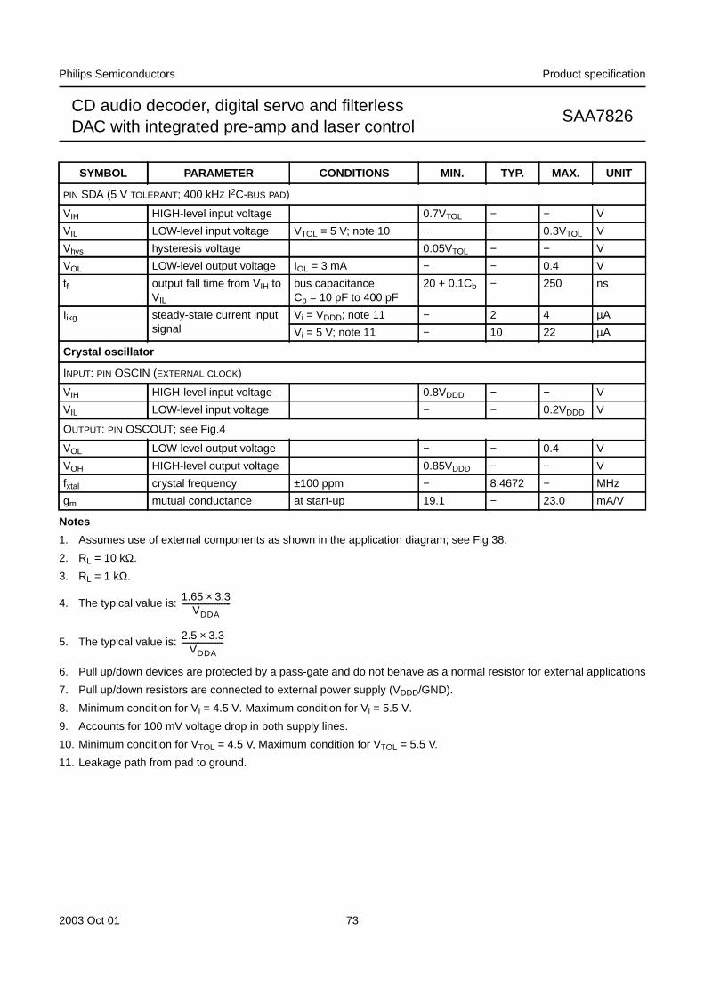
2003 Oct 01 73
Philips Semiconductors Product specification
CD audio decoder, digital servo and filterlessDAC with integrated pre-amp and laser control
SAA7826
Notes
1. Assumes use of external components as shown in the application diagram; see Fig 38.
2. RL = 10 kΩ.
3. RL = 1 kΩ.
4. The typical value is:
5. The typical value is:
6. Pull up/down devices are protected by a pass-gate and do not behave as a normal resistor for external applications
7. Pull up/down resistors are connected to external power supply (VDDD/GND).
8. Minimum condition for Vi = 4.5 V. Maximum condition for Vi = 5.5 V.
9. Accounts for 100 mV voltage drop in both supply lines.
10. Minimum condition for VTOL = 4.5 V, Maximum condition for VTOL = 5.5 V.
11. Leakage path from pad to ground.
PIN SDA (5 V TOLERANT; 400 kHZ I2C-BUS PAD)
VIH HIGH-level input voltage 0.7VTOL − − V
VIL LOW-level input voltage VTOL = 5 V; note 10 − − 0.3VTOL V
Vhys hysteresis voltage 0.05VTOL − − V
VOL LOW-level output voltage IOL = 3 mA − − 0.4 V
tf output fall time from VIH toVIL
bus capacitanceCb = 10 pF to 400 pF
20 + 0.1Cb − 250 ns
Iikg steady-state current inputsignal
Vi = VDDD; note 11 − 2 4 µA
Vi = 5 V; note 11 − 10 22 µA
Crystal oscillator
INPUT: PIN OSCIN (EXTERNAL CLOCK)
VIH HIGH-level input voltage 0.8VDDD − − V
VIL LOW-level input voltage − − 0.2VDDD V
OUTPUT: PIN OSCOUT; see Fig.4
VOL LOW-level output voltage − − 0.4 V
VOH HIGH-level output voltage 0.85VDDD − − V
fxtal crystal frequency ±100 ppm − 8.4672 − MHz
gm mutual conductance at start-up 19.1 − 23.0 mA/V
SYMBOL PARAMETER CONDITIONS MIN. TYP. MAX. UNIT
1.65 3.3×VDDA
--------------------------
2.5 3.3×VDDA
----------------------
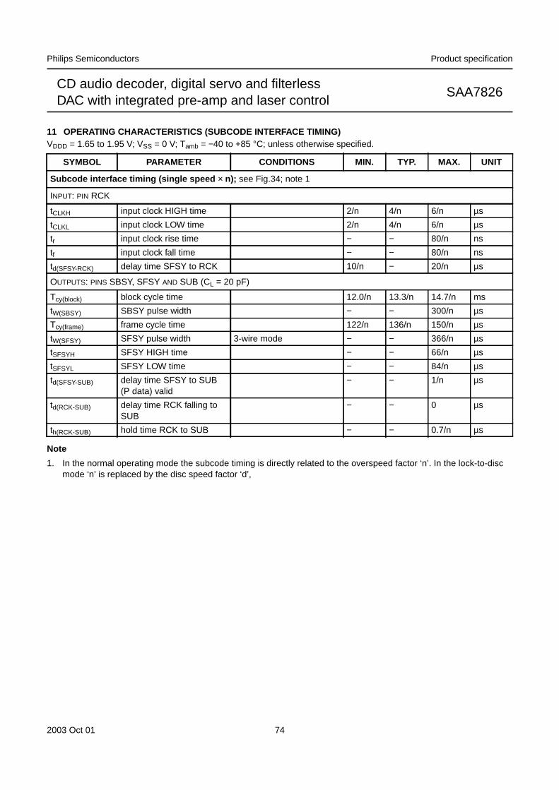
2003 Oct 01 74
Philips Semiconductors Product specification
CD audio decoder, digital servo and filterlessDAC with integrated pre-amp and laser control
SAA7826
11 OPERATING CHARACTERISTICS (SUBCODE INTERFACE TIMING)VDDD = 1.65 to 1.95 V; VSS = 0 V; Tamb = −40 to +85 °C; unless otherwise specified.
Note
1. In the normal operating mode the subcode timing is directly related to the overspeed factor ‘n’. In the lock-to-discmode ‘n’ is replaced by the disc speed factor ‘d’,
SYMBOL PARAMETER CONDITIONS MIN. TYP. MAX. UNIT
Subcode interface timing (single speed × n); see Fig.34; note 1
INPUT: PIN RCK
tCLKH input clock HIGH time 2/n 4/n 6/n µs
tCLKL input clock LOW time 2/n 4/n 6/n µs
tr input clock rise time − − 80/n ns
tf input clock fall time − − 80/n ns
td(SFSY-RCK) delay time SFSY to RCK 10/n − 20/n µs
OUTPUTS: PINS SBSY, SFSY AND SUB (CL = 20 pF)
Tcy(block) block cycle time 12.0/n 13.3/n 14.7/n ms
tW(SBSY) SBSY pulse width − − 300/n µs
Tcy(frame) frame cycle time 122/n 136/n 150/n µs
tW(SFSY) SFSY pulse width 3-wire mode − − 366/n µs
tSFSYH SFSY HIGH time − − 66/n µs
tSFSYL SFSY LOW time − − 84/n µs
td(SFSY-SUB) delay time SFSY to SUB(P data) valid
− − 1/n µs
td(RCK-SUB) delay time RCK falling toSUB
− − 0 µs
th(RCK-SUB) hold time RCK to SUB − − 0.7/n µs
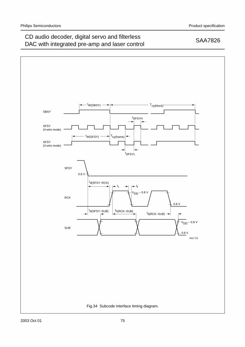
2003 Oct 01 75
Philips Semiconductors Product specification
CD audio decoder, digital servo and filterlessDAC with integrated pre-amp and laser control
SAA7826
handbook, full pagewidth tW(SBSY)
tW(SFSY)
tr
VDD – 0.8 V
VDD – 0.8 V
tSFSYL
tSFSYH
Tcy(block)
Tcy(frame)
tf
td(SFSY−RCK)
td(SFSY−SUB) th(RCK−SUB) td(RCK−SUB)
SBSY
SFSY
RCK
SUB
SFSY(4-wire mode)
SFSY(3-wire mode)
0.8 V
0.8 V
0.8 V
MGL718
Fig.34 Subcode interface timing diagram.
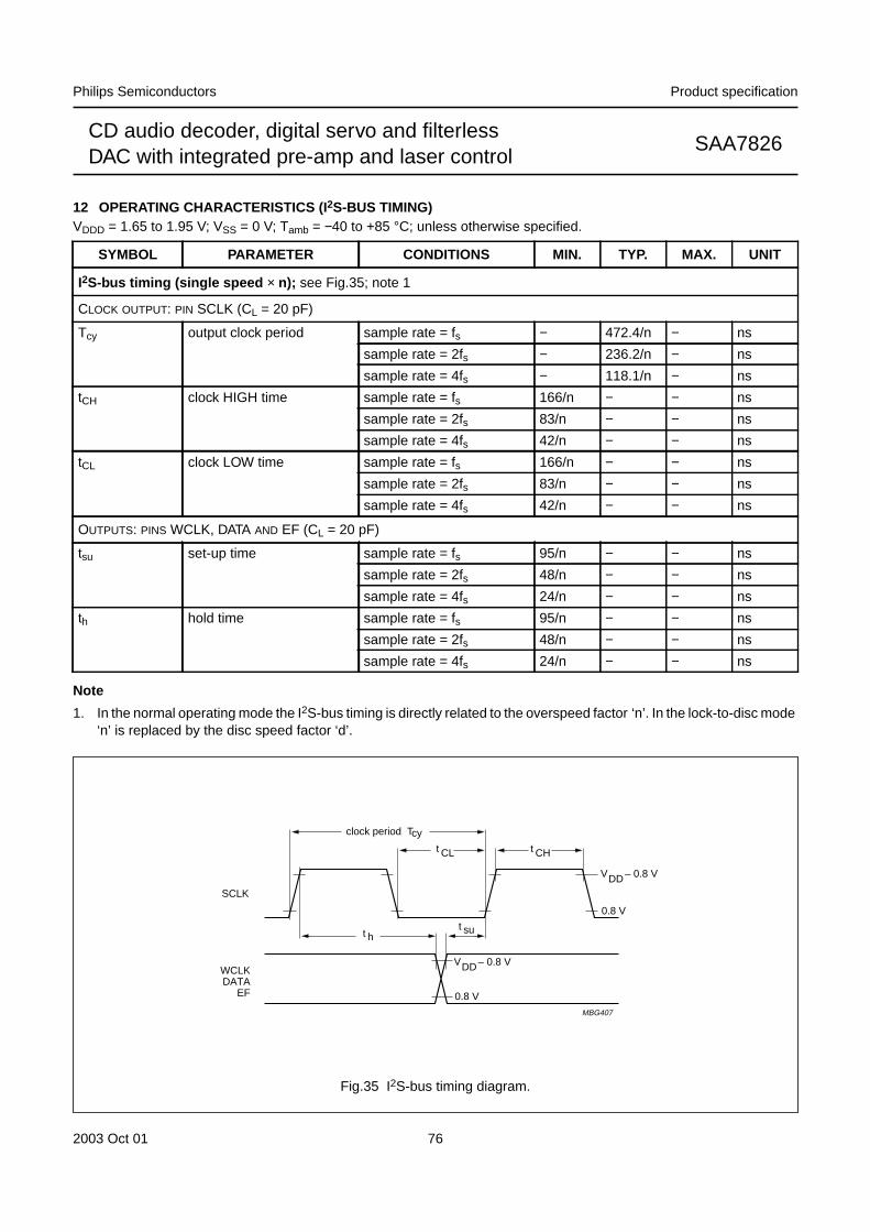
2003 Oct 01 76
Philips Semiconductors Product specification
CD audio decoder, digital servo and filterlessDAC with integrated pre-amp and laser control
SAA7826
12 OPERATING CHARACTERISTICS (I 2S-BUS TIMING)VDDD = 1.65 to 1.95 V; VSS = 0 V; Tamb = −40 to +85 °C; unless otherwise specified.
Note
1. In the normal operating mode the I2S-bus timing is directly related to the overspeed factor ‘n’. In the lock-to-disc mode‘n’ is replaced by the disc speed factor ‘d’.
SYMBOL PARAMETER CONDITIONS MIN. TYP. MAX. UNIT
I2S-bus timing (single speed × n); see Fig.35; note 1
CLOCK OUTPUT: PIN SCLK (CL = 20 pF)
Tcy output clock period sample rate = fs − 472.4/n − ns
sample rate = 2fs − 236.2/n − ns
sample rate = 4fs − 118.1/n − ns
tCH clock HIGH time sample rate = fs 166/n − − ns
sample rate = 2fs 83/n − − ns
sample rate = 4fs 42/n − − ns
tCL clock LOW time sample rate = fs 166/n − − ns
sample rate = 2fs 83/n − − ns
sample rate = 4fs 42/n − − ns
OUTPUTS: PINS WCLK, DATA AND EF (CL = 20 pF)
tsu set-up time sample rate = fs 95/n − − ns
sample rate = 2fs 48/n − − ns
sample rate = 4fs 24/n − − ns
th hold time sample rate = fs 95/n − − ns
sample rate = 2fs 48/n − − ns
sample rate = 4fs 24/n − − ns
DDV – 0.8 V
0.8 V
DDV – 0.8 V
0.8 V
t CH
MBG407
t CL
clock period Tcy
SCLK
WCLKDATA
EF
t ht su
Fig.35 I2S-bus timing diagram.
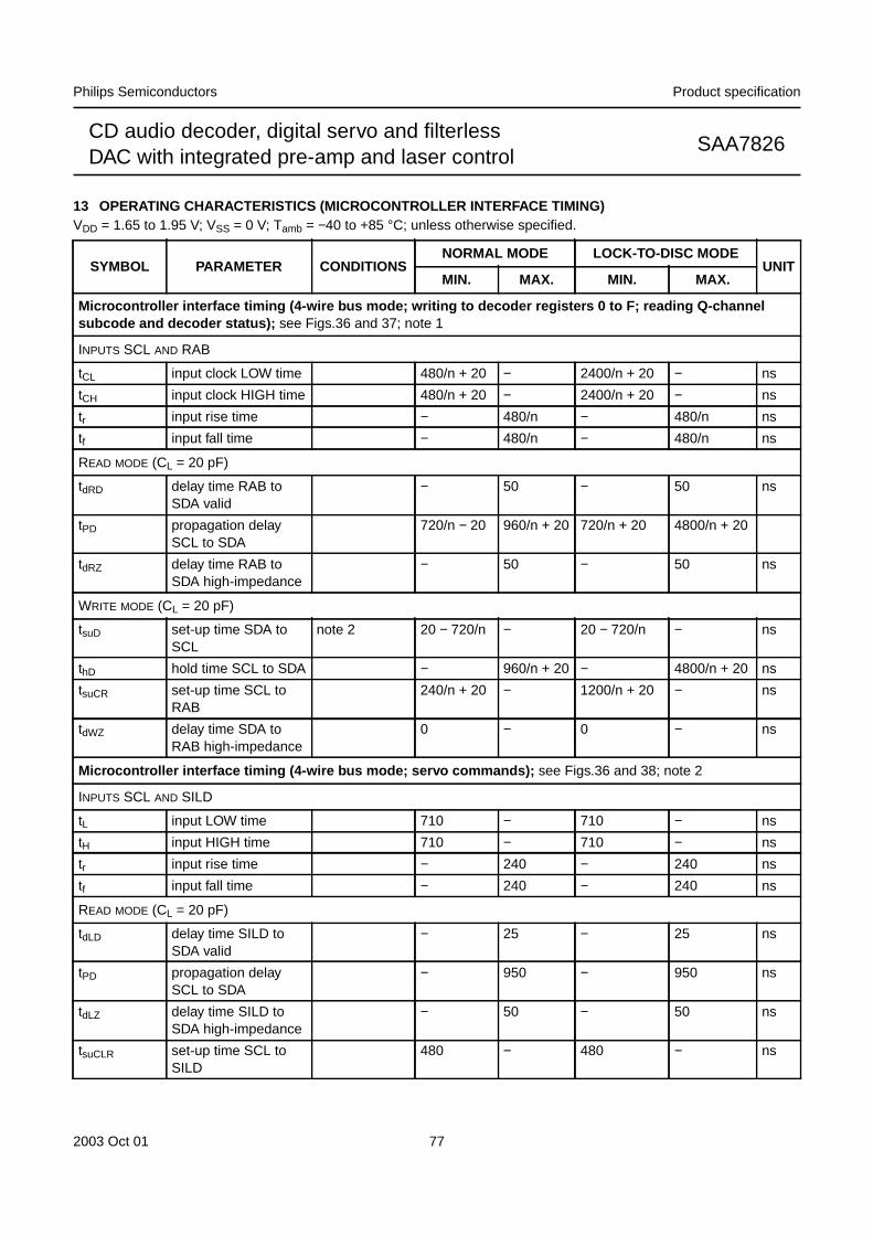
2003 Oct 01 77
Philips Semiconductors Product specification
CD audio decoder, digital servo and filterlessDAC with integrated pre-amp and laser control
SAA7826
13 OPERATING CHARACTERISTICS (MICROCONTROLLER INTERFACE TIMING)VDD = 1.65 to 1.95 V; VSS = 0 V; Tamb = −40 to +85 °C; unless otherwise specified.
SYMBOL PARAMETER CONDITIONSNORMAL MODE LOCK-TO-DISC MODE
UNITMIN. MAX. MIN. MAX.
Microcontroller interface timing (4-wire bus mode; writing to decoder registers 0 to F; reading Q-channelsubcode and decoder status); see Figs.36 and 37; note 1
INPUTS SCL AND RAB
tCL input clock LOW time 480/n + 20 − 2400/n + 20 − ns
tCH input clock HIGH time 480/n + 20 − 2400/n + 20 − ns
tr input rise time − 480/n − 480/n ns
tf input fall time − 480/n − 480/n ns
READ MODE (CL = 20 pF)
tdRD delay time RAB toSDA valid
− 50 − 50 ns
tPD propagation delaySCL to SDA
720/n − 20 960/n + 20 720/n + 20 4800/n + 20
tdRZ delay time RAB toSDA high-impedance
− 50 − 50 ns
WRITE MODE (CL = 20 pF)
tsuD set-up time SDA toSCL
note 2 20 − 720/n − 20 − 720/n − ns
thD hold time SCL to SDA − 960/n + 20 − 4800/n + 20 ns
tsuCR set-up time SCL toRAB
240/n + 20 − 1200/n + 20 − ns
tdWZ delay time SDA toRAB high-impedance
0 − 0 − ns
Microcontroller interface timing (4-wire bus mode; servo commands); see Figs.36 and 38; note 2
INPUTS SCL AND SILD
tL input LOW time 710 − 710 − ns
tH input HIGH time 710 − 710 − ns
tr input rise time − 240 − 240 ns
tf input fall time − 240 − 240 ns
READ MODE (CL = 20 pF)
tdLD delay time SILD toSDA valid
− 25 − 25 ns
tPD propagation delaySCL to SDA
− 950 − 950 ns
tdLZ delay time SILD toSDA high-impedance
− 50 − 50 ns
tsuCLR set-up time SCL toSILD
480 − 480 − ns
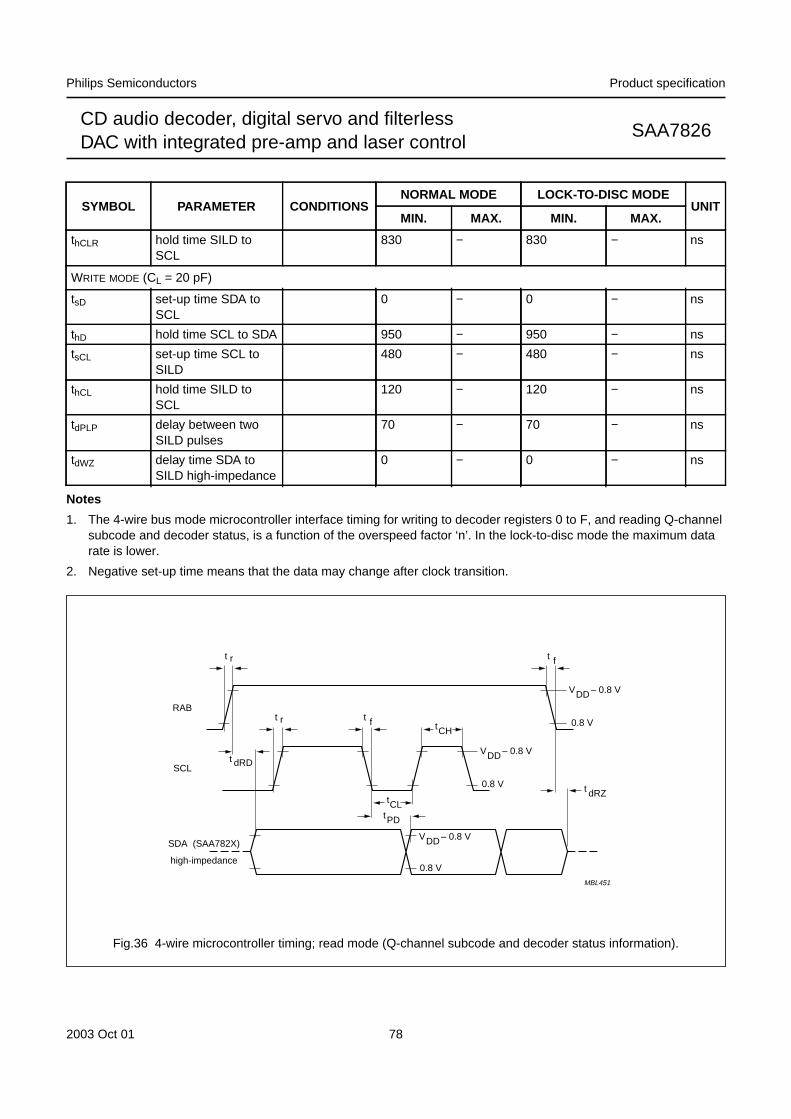
2003 Oct 01 78
Philips Semiconductors Product specification
CD audio decoder, digital servo and filterlessDAC with integrated pre-amp and laser control
SAA7826
Notes
1. The 4-wire bus mode microcontroller interface timing for writing to decoder registers 0 to F, and reading Q-channelsubcode and decoder status, is a function of the overspeed factor ‘n’. In the lock-to-disc mode the maximum datarate is lower.
2. Negative set-up time means that the data may change after clock transition.
thCLR hold time SILD toSCL
830 − 830 − ns
WRITE MODE (CL = 20 pF)
tsD set-up time SDA toSCL
0 − 0 − ns
thD hold time SCL to SDA 950 − 950 − ns
tsCL set-up time SCL toSILD
480 − 480 − ns
thCL hold time SILD toSCL
120 − 120 − ns
tdPLP delay between twoSILD pulses
70 − 70 − ns
tdWZ delay time SDA toSILD high-impedance
0 − 0 − ns
SYMBOL PARAMETER CONDITIONSNORMAL MODE LOCK-TO-DISC MODE
UNITMIN. MAX. MIN. MAX.
SDA (SAA782X)
SCL
RAB
t r
DDV – 0.8 V
0.8 Vt r t f
t f
DDV – 0.8 V
0.8 V
DDV – 0.8 V
0.8 V
tPD
tCL
tCH
t dRD
t dRZ
high-impedance
MBL451
Fig.36 4-wire microcontroller timing; read mode (Q-channel subcode and decoder status information).
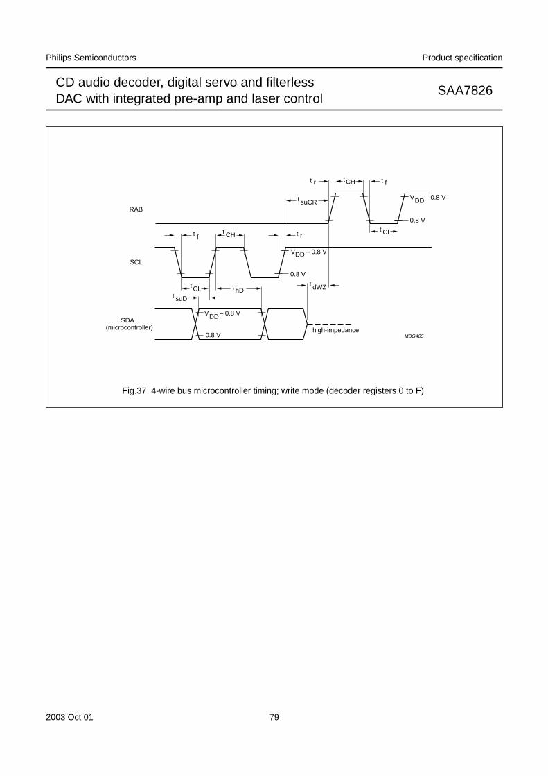
2003 Oct 01 79
Philips Semiconductors Product specification
CD audio decoder, digital servo and filterlessDAC with integrated pre-amp and laser control
SAA7826
handbook, full pagewidth
SCL
RAB
t rt f
DDV – 0.8 V
0.8 V
DDV – 0.8 V
0.8 V
t hDtCL
t CH
t dWZ
MBG405
t r t f
DDV – 0.8 V
0.8 Vt CL
tCH
t suCR
t suD
SDA (microcontroller) high-impedance
Fig.37 4-wire bus microcontroller timing; write mode (decoder registers 0 to F).
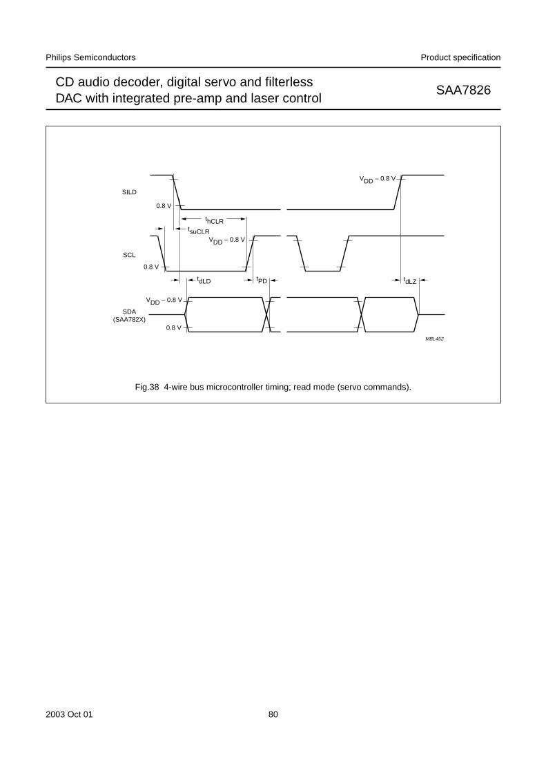
2003 Oct 01 80
Philips Semiconductors Product specification
CD audio decoder, digital servo and filterlessDAC with integrated pre-amp and laser control
SAA7826
handbook, full pagewidth
tdLD
thCLRtsuCLR
tPD tdLZ
0.8 V
0.8 V
0.8 V
VDD – 0.8 V
VDD – 0.8 V
VDD – 0.8 V
SILD
SCL
SDA(SAA782X)
MBL452
Fig.38 4-wire bus microcontroller timing; read mode (servo commands).
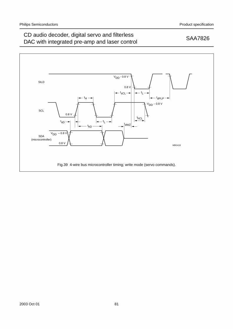
2003 Oct 01 81
Philips Semiconductors Product specification
CD audio decoder, digital servo and filterlessDAC with integrated pre-amp and laser control
SAA7826
handbook, full pagewidth
tdPLP
tLtsCL
tdWZ
thCL
tH
thD
tsD tL
0.8 V
0.8 V
0.8 V
VDD - 0.8 V
VDD – 0.8 V
VDD – 0.8 V
SILD
SCL
SDA(microcontroller)
MBG416
Fig.39 4-wire bus microcontroller timing; write mode (servo commands).
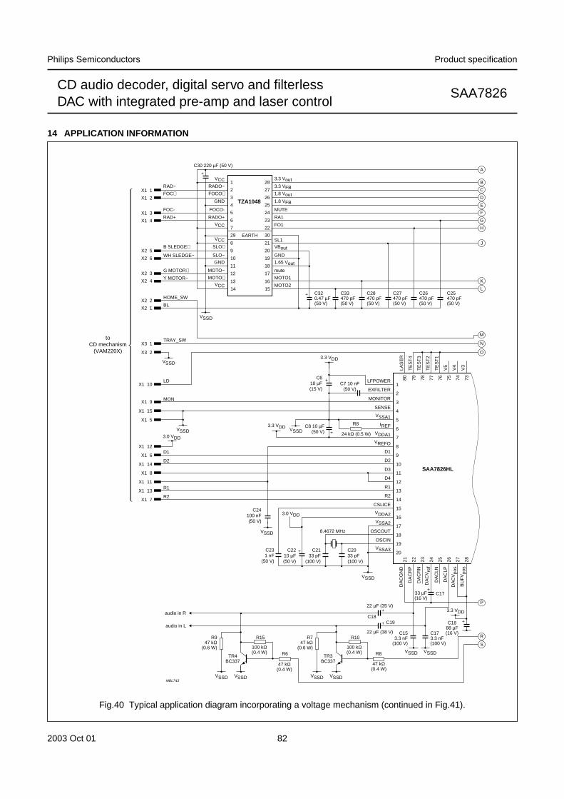
2003 Oct 01 82
Philips Semiconductors Product specification
CD audio decoder, digital servo and filterlessDAC with integrated pre-amp and laser control
SAA7826
14 APPLICATION INFORMATION
handbook, full pagewidth
SAA7826HL
MBL743
LAS
ER
TE
ST
4
TE
ST
3
TE
ST
2
TE
ST
1
V5
V4
V3
DA
CG
ND
21 22 23 24 25 26 27 28
79 78 77 76 75 74 7380D
AC
RP
DA
CR
N
DA
CV
ref
DA
CLN
DA
CLP
DA
CV
pos
BU
FV
pos
LFPOWER
EXFILTER
MONITOR
SENSE
VSSA1
IREF
VDDA1
VREFO
D1
D2
D3
D4
R1
R2
CSLICE
VDDA2
VSSA2
OSCOUT8.4672 MHz
24 kΩ (0.5 W)
R8
VSSD
VSSD
OSCIN
VSSA3
3
1
2
6
4
5
9
7
8
12
10
11
15
13
14
18
16
17
19
20
MOTO1
mute
MOTO216
17
15
33 µF(16 V)
C1888 µF(16 V)C15
3.3 nF(100 V)
C173.3 nF(100 V)
C18C19
R8
R10
22 µF (35 V)
22 µF (38 V)
47 kΩ(0.4 W)
100 kΩ(0.4 W)
R747 kΩ
(0.6 W)
R947 kΩ
(0.6 W)
audio in R
audio in L
R6
47 kΩ(0.4 W)
C17
VSSDVSSD
VSSDVSSD
C25470 pF(50 V)
C26470 pF(50 V)
C27470 pF(50 V)
C28470 pF(50 V)
C33470 pF(50 V)
C320.47 µF(50 V)
C30 220 µF (50 V)
3.0 VDD
3.3 VDD
3.0 VDD
3.3 VDD
EARTH
TZA1048
VSSD
VSSD
VSSD
VSSD
C2033 pF(100 V)
C2133 pF
(100 V)
C231 nF
(50 V)
C24100 nF(50 V)
C2210 µF(50 V)
C8 10 µF(50 V)
C610 µF(15 V)
C7 10 nF(50 V)
18
GND19
VBout20
SL121
FO122
30
RA123
MUTE24
25
26
3.3 VFB27
3.3 Vout
1.8 Vout
1.65 Vout
1.8 VFB
MOTO+MOTO−
VCC
SLO−
SLO+B SLEDGE+
WH SLEDGE−
G MOTOR+Y MOTOR−
HOME_SW
TRAY_SW
LD
MON
toCD mechanism
(VAM220X)
D1
D2
R1
R2
BL
VCC
VCC
RADO+
FOCO-
RADO−VCC
FOCO+
RAD+
FOC-
RAD−FOC+
GND
GND
X1 1
X1 2
X1 3
X1 4
X2 5
X2 6
X2 3
X2 4
X2 2
X2 1
X3 1
X3 2
TR3BC337
3.3 VDD
X1 10
X1 9
X1 15
X1 5
X1 12
X1 6
X1 14
X1 8
X1 11
X1 13
X1 7
28
13
12
14
11
10
9
8
7
29
6
5
4
3
2
1
VSSDVSSD
TR4BC337
R15
100 kΩ(0.4 W)
B
A
C
D
E
F
G
H
J
K
L
M
O
N
P
R
S
Fig.40 Typical application diagram incorporating a voltage mechanism (continued in Fig.41).
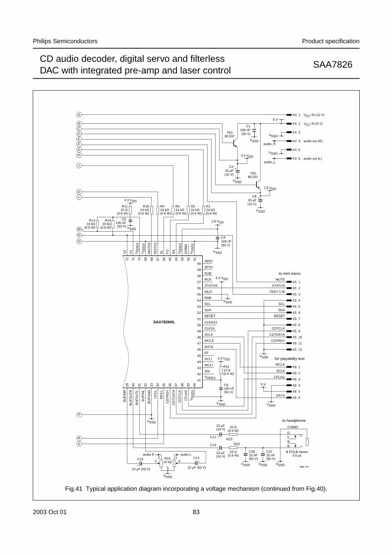
2003 Oct 01 83
Philips Semiconductors Product specification
CD audio decoder, digital servo and filterlessDAC with integrated pre-amp and laser control
SAA7826
handbook, full pagewidth
SAA7826HL
MBL744
V2
V1
VD
DD
3
VS
SD
3
MO
TO
2
MO
TO
1
SL
FO
RA
VD
DD
2
DO
BM
VS
SD
2
29 30 31 32 33 34 35 36 37 38 39 40
72 71 70 69 68 67 66 65 64 63 62 61
BU
FIN
R
BU
FO
UT
R
BU
FO
UT
L
BU
FIN
L
BU
FG
ND
LKIL
L
RK
ILL
CD
TR
DY
CD
TD
AT
A
CD
TC
LK
CF
LAG
VS
SD
1
SBSY
C4100 nF(50 V)
C1100 nF(50 V)
C233 µF(16 V)
SFSY
VSSD
to mini micro
for playability test
to headphone
VSSD
3.3 VDD
1.8 VDD
SUB58
60
59
55
57
56
52
54
53
49
51
50
46
48
47
43
45
44
42
41
RCK
STATUS
SILD
MUTE
STATUS
TRAY 5 W
RAB
SCL
SDA
RESET
CLK4/12
CLK16
SCLK
WCLK
DATA
EF
SCLI
WCLI
SDI
VDDD1
R1210 Ω(0.6 W)
C9100 nF(50 V)
SCL
SDA
RESET
CDTCLK
CDTDATA
CDTRDY
WCLK
SCLK
CFLAG
DATA
C833 µF(16 V)
VSSD
5 V
VSSD
C11
33 µF(16 V)
10 Ω(0.6 W)
33 µF(16 V)
R1010 kΩ
10 µF (50 V)10 µF (50 V)
10 Ω(0.6 W)
C10
C14C16 123 4
audio Laudio R
5
R23
R22
VSSD
VSSD
VSSD
3.3 VDD
VSSD
3.3 VDD
C5100 nF(50 V)
R1410 kΩ
(0.6 W)
R1624 kΩ
(0.6 W)
R1110 Ω
(0.6 W)
R424 kΩ(0.6 W)
R1310 kΩ
(0.6 W)
R324 kΩ(0.6 W)
R224 kΩ(0.6 W)
R124 kΩ(0.6 W)
VCC IN (12 V)
VSSDVSSD
VSSD
VSSD
3.3 VDD
TR1BC337
TR2BC337
1.8 VDD
X4 1
VCC IN (5 V)X4 2
X4 3
audio out (R)X4 4
X4 5
audio out (L)X4 6
X5 1
X5 2
X5 3
X5 4
X5 5
X5 6
X5 7
X5 8
X5 9
X5 10
X5 11
X5 12
X6 1
X6 2
X6 3
X6 4
X6 5
X6 6
C3610 nF(50 V)
VSSD
VSSD
VSSD
C3710 nF(50 V)
O BMD
DFBB
B POLB stereo3.5 µs
5 V
audio_R
audio_L
VSSD
B
A
C
D
E
F
G
H
J
K
L
M
O
N
P
R
S
Fig.41 Typical application diagram incorporating a voltage mechanism (continued from Fig.40).
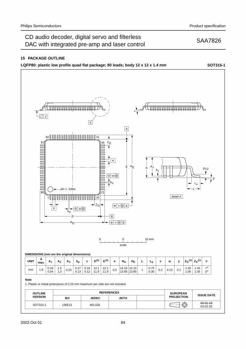
2003 Oct 01 84
Philips Semiconductors Product specification
CD audio decoder, digital servo and filterlessDAC with integrated pre-amp and laser control
SAA7826
15 PACKAGE OUTLINE
UNITA
max. A1 A2 A3 bp c E(1) e HE L L p Zywv θ
REFERENCESOUTLINEVERSION
EUROPEANPROJECTION ISSUE DATE
IEC JEDEC JEITA
mm 1.6 0.160.04
1.51.3 0.25
0.270.13
0.180.12
12.111.9 0.5
14.1513.85
1.451.05
70
o
o0.15 0.10.21
DIMENSIONS (mm are the original dimensions)
Note
1. Plastic or metal protrusions of 0.25 mm maximum per side are not included.
0.750.30
SOT315-1 136E15 MS-02600-01-1903-02-25
D(1) (1)(1)
12.111.9
HD
14.1513.85
EZ
1.451.05
D
bp
e
θ
EA1
A
Lp
detail X
L
(A )3
B
20
c
DH
bp
EH A2
v M B
D
ZD
A
ZE
e
v M A
X
1
80
61
60 41
40
21
y
pin 1 index
w M
w M
0 5 10 mm
scale
LQFP80: plastic low profile quad flat package; 80 leads; body 12 x 12 x 1.4 mm SOT315-1
2003 Oct 01 85
Philips Semiconductors Product specification
CD audio decoder, digital servo and filterlessDAC with integrated pre-amp and laser control
SAA7826
16 SOLDERING
16.1 Introduction to soldering surface mountpackages
This text gives a very brief insight to a complex technology.A more in-depth account of soldering ICs can be found inour “Data Handbook IC26; Integrated Circuit Packages”(document order number 9398 652 90011).
There is no soldering method that is ideal for all surfacemount IC packages. Wave soldering can still be used forcertain surface mount ICs, but it is not suitable for fine pitchSMDs. In these situations reflow soldering isrecommended.
16.2 Reflow soldering
Reflow soldering requires solder paste (a suspension offine solder particles, flux and binding agent) to be appliedto the printed-circuit board by screen printing, stencilling orpressure-syringe dispensing before package placement.Driven by legislation and environmental forces theworldwide use of lead-free solder pastes is increasing.
Several methods exist for reflowing; for example,convection or convection/infrared heating in a conveyortype oven. Throughput times (preheating, soldering andcooling) vary between 100 and 200 seconds dependingon heating method.
Typical reflow peak temperatures range from215 to 270 °C depending on solder paste material. Thetop-surface temperature of the packages shouldpreferably be kept:
• below 220 °C (SnPb process) or below 245 °C (Pb-freeprocess)
– for all BGA and SSOP-T packages
– for packages with a thickness ≥ 2.5 mm
– for packages with a thickness < 2.5 mm and avolume ≥ 350 mm3 so called thick/large packages.
• below 235 °C (SnPb process) or below 260 °C (Pb-freeprocess) for packages with a thickness < 2.5 mm and avolume < 350 mm3 so called small/thin packages.
Moisture sensitivity precautions, as indicated on packing,must be respected at all times.
16.3 Wave soldering
Conventional single wave soldering is not recommendedfor surface mount devices (SMDs) or printed-circuit boardswith a high component density, as solder bridging andnon-wetting can present major problems.
To overcome these problems the double-wave solderingmethod was specifically developed.
If wave soldering is used the following conditions must beobserved for optimal results:
• Use a double-wave soldering method comprising aturbulent wave with high upward pressure followed by asmooth laminar wave.
• For packages with leads on two sides and a pitch (e):
– larger than or equal to 1.27 mm, the footprintlongitudinal axis is preferred to be parallel to thetransport direction of the printed-circuit board;
– smaller than 1.27 mm, the footprint longitudinal axismust be parallel to the transport direction of theprinted-circuit board.
The footprint must incorporate solder thieves at thedownstream end.
• For packages with leads on four sides, the footprint mustbe placed at a 45° angle to the transport direction of theprinted-circuit board. The footprint must incorporatesolder thieves downstream and at the side corners.
During placement and before soldering, the package mustbe fixed with a droplet of adhesive. The adhesive can beapplied by screen printing, pin transfer or syringedispensing. The package can be soldered after theadhesive is cured.
Typical dwell time of the leads in the wave ranges from3 to 4 seconds at 250 °C or 265 °C, depending on soldermaterial applied, SnPb or Pb-free respectively.
A mildly-activated flux will eliminate the need for removalof corrosive residues in most applications.
16.4 Manual soldering
Fix the component by first soldering twodiagonally-opposite end leads. Use a low voltage (24 V orless) soldering iron applied to the flat part of the lead.Contact time must be limited to 10 seconds at up to300 °C.
When using a dedicated tool, all other leads can besoldered in one operation within 2 to 5 seconds between270 and 320 °C.
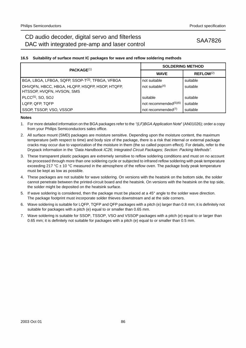
2003 Oct 01 86
Philips Semiconductors Product specification
CD audio decoder, digital servo and filterlessDAC with integrated pre-amp and laser control
SAA7826
16.5 Suitability of surface mount IC packages for wave and reflow soldering methods
Notes
1. For more detailed information on the BGA packages refer to the “(LF)BGA Application Note” (AN01026); order a copyfrom your Philips Semiconductors sales office.
2. All surface mount (SMD) packages are moisture sensitive. Depending upon the moisture content, the maximumtemperature (with respect to time) and body size of the package, there is a risk that internal or external packagecracks may occur due to vaporization of the moisture in them (the so called popcorn effect). For details, refer to theDrypack information in the “Data Handbook IC26; Integrated Circuit Packages; Section: Packing Methods”.
3. These transparent plastic packages are extremely sensitive to reflow soldering conditions and must on no accountbe processed through more than one soldering cycle or subjected to infrared reflow soldering with peak temperatureexceeding 217 °C ± 10 °C measured in the atmosphere of the reflow oven. The package body peak temperaturemust be kept as low as possible.
4. These packages are not suitable for wave soldering. On versions with the heatsink on the bottom side, the soldercannot penetrate between the printed-circuit board and the heatsink. On versions with the heatsink on the top side,the solder might be deposited on the heatsink surface.
5. If wave soldering is considered, then the package must be placed at a 45° angle to the solder wave direction.The package footprint must incorporate solder thieves downstream and at the side corners.
6. Wave soldering is suitable for LQFP, TQFP and QFP packages with a pitch (e) larger than 0.8 mm; it is definitely notsuitable for packages with a pitch (e) equal to or smaller than 0.65 mm.
7. Wave soldering is suitable for SSOP, TSSOP, VSO and VSSOP packages with a pitch (e) equal to or larger than0.65 mm; it is definitely not suitable for packages with a pitch (e) equal to or smaller than 0.5 mm.
PACKAGE (1)SOLDERING METHOD
WAVE REFLOW (2)
BGA, LBGA, LFBGA, SQFP, SSOP-T(3), TFBGA, VFBGA not suitable suitable
DHVQFN, HBCC, HBGA, HLQFP, HSQFP, HSOP, HTQFP,HTSSOP, HVQFN, HVSON, SMS
not suitable(4) suitable
PLCC(5), SO, SOJ suitable suitable
LQFP, QFP, TQFP not recommended(5)(6) suitable
SSOP, TSSOP, VSO, VSSOP not recommended(7) suitable
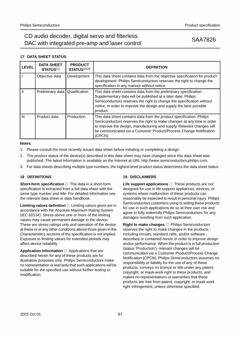
2003 Oct 01 87
Philips Semiconductors Product specification
CD audio decoder, digital servo and filterlessDAC with integrated pre-amp and laser control
SAA7826
17 DATA SHEET STATUS
Notes
1. Please consult the most recently issued data sheet before initiating or completing a design.
2. The product status of the device(s) described in this data sheet may have changed since this data sheet waspublished. The latest information is available on the Internet at URL http://www.semiconductors.philips.com.
3. For data sheets describing multiple type numbers, the highest-level product status determines the data sheet status.
LEVELDATA SHEET
STATUS(1)PRODUCT
STATUS(2)(3) DEFINITION
I Objective data Development This data sheet contains data from the objective specification for productdevelopment. Philips Semiconductors reserves the right to change thespecification in any manner without notice.
II Preliminary data Qualification This data sheet contains data from the preliminary specification.Supplementary data will be published at a later date. PhilipsSemiconductors reserves the right to change the specification withoutnotice, in order to improve the design and supply the best possibleproduct.
III Product data Production This data sheet contains data from the product specification. PhilipsSemiconductors reserves the right to make changes at any time in orderto improve the design, manufacturing and supply. Relevant changes willbe communicated via a Customer Product/Process Change Notification(CPCN).
18 DEFINITIONS
Short-form specification The data in a short-formspecification is extracted from a full data sheet with thesame type number and title. For detailed information seethe relevant data sheet or data handbook.
Limiting values definition Limiting values given are inaccordance with the Absolute Maximum Rating System(IEC 60134). Stress above one or more of the limitingvalues may cause permanent damage to the device.These are stress ratings only and operation of the deviceat these or at any other conditions above those given in theCharacteristics sections of the specification is not implied.Exposure to limiting values for extended periods mayaffect device reliability.
Application information Applications that aredescribed herein for any of these products are forillustrative purposes only. Philips Semiconductors makeno representation or warranty that such applications will besuitable for the specified use without further testing ormodification.
19 DISCLAIMERS
Life support applications These products are notdesigned for use in life support appliances, devices, orsystems where malfunction of these products canreasonably be expected to result in personal injury. PhilipsSemiconductors customers using or selling these productsfor use in such applications do so at their own risk andagree to fully indemnify Philips Semiconductors for anydamages resulting from such application.
Right to make changes Philips Semiconductorsreserves the right to make changes in the products -including circuits, standard cells, and/or software -described or contained herein in order to improve designand/or performance. When the product is in full production(status ‘Production’), relevant changes will becommunicated via a Customer Product/Process ChangeNotification (CPCN). Philips Semiconductors assumes noresponsibility or liability for the use of any of theseproducts, conveys no licence or title under any patent,copyright, or mask work right to these products, andmakes no representations or warranties that theseproducts are free from patent, copyright, or mask workright infringement, unless otherwise specified.
2003 Oct 01 88
Philips Semiconductors Product specification
CD audio decoder, digital servo and filterlessDAC with integrated pre-amp and laser control
SAA7826
20 PURCHASE OF PHILIPS I2C COMPONENTS
Purchase of Philips I2C components conveys a license under the Philips’ I2C patent to use thecomponents in the I2C system provided the system conforms to the I2C specification defined byPhilips. This specification can be ordered using the code 9398 393 40011.
© Koninklijke Philips Electronics N.V. 2003 SCA75All rights are reserved. Reproduction in whole or in part is prohibited without the prior written consent of the copyright owner.
The information presented in this document does not form part of any quotation or contract, is believed to be accurate and reliable and may be changedwithout notice. No liability will be accepted by the publisher for any consequence of its use. Publication thereof does not convey nor imply any licenseunder patent- or other industrial or intellectual property rights.
Philips Semiconductors – a worldwide company
Contact information
For additional information please visit http://www.semiconductors.philips.com . Fax: +31 40 27 24825For sales offices addresses send e-mail to: [email protected] .
Printed in The Netherlands R04/02/pp89 Date of release: 2003 Oct 01 Document order number: 9397 750 12011