SA614A Low power FM IF system - NXP Semiconductors. General description The SA614A is an improved...
28
1. General description The SA614A is an improved monolithic low-power FM IF system. It incorporates two limiting intermediate frequency amplifiers, quadrature detector, muting, logarithmic received signal strength indicator, and voltage regulator. The SA614A features higher IF bandwidth (25 MHz) and temperature compensated RSSI and limiters permitting higher performance application compared with the SA604. The SA614A is available in a SO (surface-mounted miniature) package. 2. Features and benefits Low power consumption: 3.3 mA typical Temperature compensated logarithmic RSSI with a 90 dB dynamic range Two audio outputs - muted and unmuted Low external component count; suitable for crystal/ceramic filters Excellent sensitivity: 1.5 V across inputs pins (0.22 V into 50 matching network) for 12 dB SINAD (SIgnal-to-Noise-And-Distortion ratio) for 1 kHz tone with RF at 45 MHz and IF at 455 kHz SA614A meets cellular radio specifications 3. Applications Cellular radio FM IF High performance communication receiver Intermediate frequency amplification and detection up to 25 MHz RF level meter Spectrum analyzer Instrumentation FSK and ASK data receivers 4. Ordering information SA614A Low power FM IF system Rev. 4 — 14 February 2014 Product data sheet Table 1. Ordering information T amb = 40 C to +85 C Type number Package Name Description Version SA614AD SO16 plastic small outline package; 16 leads; body width 3.9 mm SOT109-1 SA614AHR HXQFN16 plastic thermal enhanced extremely thin quad flat package; no leads; 16 terminals; body 3 3 0.5 mm SOT1039-2
Transcript of SA614A Low power FM IF system - NXP Semiconductors. General description The SA614A is an improved...

1. General description
The SA614A is an improved monolithic low-power FM IF system. It incorporates two limiting intermediate frequency amplifiers, quadrature detector, muting, logarithmic received signal strength indicator, and voltage regulator. The SA614A features higher IF bandwidth (25 MHz) and temperature compensated RSSI and limiters permitting higher performance application compared with the SA604. The SA614A is available in a SO (surface-mounted miniature) package.
2. Features and benefits
Low power consumption: 3.3 mA typical
Temperature compensated logarithmic RSSI with a 90 dB dynamic range
Two audio outputs - muted and unmuted
Low external component count; suitable for crystal/ceramic filters
Excellent sensitivity: 1.5 V across inputs pins (0.22 V into 50 matching network) for 12 dB SINAD (SIgnal-to-Noise-And-Distortion ratio) for 1 kHz tone with RF at 45 MHz and IF at 455 kHz
SA614A meets cellular radio specifications
3. Applications
Cellular radio FM IF
High performance communication receiver
Intermediate frequency amplification and detection up to 25 MHz
RF level meter
Spectrum analyzer
Instrumentation
FSK and ASK data receivers
4. Ordering information
SA614ALow power FM IF systemRev. 4 — 14 February 2014 Product data sheet
Table 1. Ordering informationTamb = 40 C to +85 C
Type number Package
Name Description Version
SA614AD SO16 plastic small outline package; 16 leads; body width 3.9 mm SOT109-1
SA614AHR HXQFN16 plastic thermal enhanced extremely thin quad flat package; no leads; 16 terminals; body 3 3 0.5 mm
SOT1039-2

NXP Semiconductors SA614ALow power FM IF system
5. Block diagram
Pin numbers for SO16; HXQFN16 pins shown in parentheses.
Fig 1. Block diagram of SA614A
aaa-009746
VOLTAGEREGULATOR
SIGNALSTRENGTH
IFAMP
1 (14) 2 (15) 3 (16) 4 (1) 5 (2) 6 (3) 7 (4) 8 (5)
16 (13) 15 (12) 14 (11) 13 (10) 12 (9) 11 (8) 10 (7) 9 (6)
LIMITER
GND
VCCGND
MUTE
QUADDET
SA614A All information provided in this document is subject to legal disclaimers. © NXP B.V. 2014. All rights reserved.
Product data sheet Rev. 4 — 14 February 2014 2 of 28

NXP Semiconductors SA614ALow power FM IF system
6. Pinning information
6.1 Pinning
Fig 2. Pin configuration for SO16
(1) Die Attach Paddle (DAP).
Fig 3. Pin configuration for HXQFN16
SA614A
IF_AMP_DECOUPL IF_AMP_INPUT
GND IF_AMP_DECOUPL
MUTE_INPUT IF_AMP_OUTPUT
VCC GND
RSSI_OUTPUT LIMITER_INPUT
MUTE_AUD_OUTP LIMITER_DECOUPL
UNMUTE_AUD_OUTP LIMITER_DECOUPL
QUADRATURE_INPUT LIMITER_OUTPUT
aaa-009743
1
2
3
4
5
6
7
8
10
9
12
11
14
13
16
15
aaa-009745
SA614A
(1)
Transparent top view
UNMUTE_AUD_OUTP LIMITER_INPUT
MUTE_AUD_OUTP GND
RRSI_OUTP IF_AMP_OUTPUT
VCC IF_AMP_DECOUPL
QU
AD
RA
TUR
E_I
NP
UT
LIM
ITE
R_O
UTP
UT
LIM
ITE
R_D
EC
OU
PL
LIM
ITE
R_D
EC
OU
PL
MU
TE_I
NP
UT
GN
D
IF_A
MP
_DE
CO
UP
L
IF_A
MP
_IN
PU
T
4 9
3 10
2 11
1 12
5 6 7 8
16 15 14 13
terminal 1index area
SA614A All information provided in this document is subject to legal disclaimers. © NXP B.V. 2014. All rights reserved.
Product data sheet Rev. 4 — 14 February 2014 3 of 28

NXP Semiconductors SA614ALow power FM IF system
6.2 Pin description
[1] HXQFN16 package supply ground is connected to both GND pin and exposed center pad. GND pin must be connected to supply ground for proper device operation. For enhanced thermal, electrical, and board level performance, the exposed pad must be soldered to the board using a corresponding thermal pad on the board. For proper heat conduction through the board, thermal vias must be incorporated in the PCB in the thermal pad region.
Table 2. Pin description
Symbol Pin Description
SO16 HXQFN16
IF_AMP_DECOUPL 1 14 IF amplifier decoupling
GND 2 15 ground
MUTE_INPUT 3 16 mute input
VCC 4 1 supply voltage
RSSI_OUTPUT 5 2 RSSI output
MUTE_AUD_OUTP 6 3 mute audio output
UNMUTE_AUD_OUTP 7 4 unmute audio output
QUADRATURE_INPUT 8 5 quadrature input
LIMITER_OUTPUT 9 6 limiter output
LIMITER_DECOUPL 10 7 limiter decoupling
LIMITER_DECOUPL 11 8 limiter decoupling
LIMITER_INPUT 12 9 limiter input
GND 13 10[1] ground
IF_AMP_OUTPUT 14 11 IF amplifier output
IF_AMP_DECOUPL 15 12 IF amplifier decoupling
IF_AMP_INPUT 16 13 IF amplifier input
- - DAP exposed Die Attach Paddle
SA614A All information provided in this document is subject to legal disclaimers. © NXP B.V. 2014. All rights reserved.
Product data sheet Rev. 4 — 14 February 2014 4 of 28
xxxx xxxxxxxxxxxxxxxxxxxxxxxxxxxxxx x xxxxxxxxxxxxxx xxxxxxxxxx xxx xxxxxx xxxxxxxxxxxxxxxxxxxxxxx xxxxxxxxxxxxxxxxxxxxxx xxxxx xxxxxx xx xxxxxxxxxxxxxxxxxxxxxxxxxxxxx xxxxxxxxxxxxxxxxxxxxxx xxxxxxxxxxx xxxxxxx xxxxxxxxxxxxxxxxxxx xxxxxxxxxxxxxxxx xxxxxxxxxxxxxx xxxxxx xx xxxxxxxxxxxxxxxxxxxxxxxxxxxxxxxx xxxxxxxxxxxxxxxxxxxxxxxx xxxxxxx xxxxxxxxxxxxxxxxxxxxxxxxxxxxxxxxxxxxxxxxxxxxxx xxxxxxxxxxx xxxxx x x
SA
614A
Pro
du
ct data sh
NX
P S
emico
nd
ucto
7. F
un
ction
al d
GND9
eet42 kΩ
16 15 14 13 12 11 10
42 kΩ
rsS
A614A
Lo
w p
ow
er F
M IF
sys
tem
escriptio
n
aaa-009760
8
kΩ 2 kΩ
40 kΩ
80 kΩ
4.5 kΩ8 kΩ
QUADDET
All inform
ation provided
in this docum
ent is subject to leg
al disclaim
ers.©
NX
P B
.V. 2014. A
ll rights reserved.
Rev. 4 —
14 Feb
ruary 2014
5 o
f 28
Fig 4. Equivalent circuit
40 kΩ
80 kΩ
1.6kΩ
FULL WAVERECT.
VOLTREG
VOLTREG
1 2
GND
3 4 5 6 7
VCC
VEE
VCC
BANDGAP VOLT
VOLTAGE/CURRENT CONVERTER
40 kΩ
2
55 kΩ 55 kΩ
40 kΩ
80 kΩ
1.6kΩ
35 kΩ
700 Ω
700 Ω
7 kΩ
FULL WAVERECT.
MUTE
VCC

NXP Semiconductors SA614ALow power FM IF system
8. Limiting values
9. Thermal characteristics
10. Static characteristics
Table 3. Limiting valuesIn accordance with the Absolute Maximum Rating System (IEC 60134).
Symbol Parameter Conditions Min Max Unit
VCC supply voltage - 9 V
Tstg storage temperature 65 +150 C
Tamb ambient temperature operating 40 +85 C
Table 4. Thermal characteristics
Symbol Parameter Conditions Max Unit
Zth(j-a) transient thermal impedance from junction to ambient
SA614AD (SO16) 90 K/W
SA614AHR (HXQFN16) 75 K/W
Table 5. Static characteristicsVCC = 3 V; Tamb = 25 C; unless specified otherwise.
Symbol Parameter Conditions Min Typ Max Unit
ICC supply current 2.5 3.3 4.0 mA
VCC supply voltage 4.5 - 8.0 V
Vth threshold voltage mute switch-on 1.7 - - V
mute switch-off - - 1.0 V
SA614A All information provided in this document is subject to legal disclaimers. © NXP B.V. 2014. All rights reserved.
Product data sheet Rev. 4 — 14 February 2014 6 of 28

NXP Semiconductors SA614ALow power FM IF system
11. Dynamic characteristics
[1] SA614A data sheets refer to power at 50 input termination; about 21 dB less power actually enters the internal 1.5 k input.
SA614A (50 ) - SA614A (1.5 k)/SA615 (1.5 k)
97 dBm - 118 dBm
47 dBm - 68 dBm
+3 dBm - 18 dBm
The SA615 and SA614A are both derived from the same basic die. The SA615 performance plots are directly applicable to the SA614A.
Table 6. Dynamic characteristicsTamb = 25 C; VCC = 6 V; unless specified otherwise. IF frequency = 455 kHz; IF level = 47 dBm; FM modulation = 1 kHz with 8 kHz peak deviation. Audio output with de-emphasis filter and C-message weighted filter. Test circuit Figure 14. The parameters listed below are tested using automatic test equipment to assure consistent electrical characteristics. The limits do not represent the ultimate performance limits of the device. Use of an optimized RF layout will improves many of the listed parameters.
Symbol Parameter Conditions Min Typ Max Unit
input limiting 3 dB test at pin IF_AMP_INPUT: per 50 - 92 - dBm
AM rejection 80 % AM 1 kHz 25 33 - dB
recovered audio level 15 nF de-emphasis 60 175 260 mVRMS
150 pF de-emphasis - 530 - mVRMS
THD total harmonic distortion 30 42 - dB
S/N signal-to-noise ratio no modulation for noise - 68 - dB
RSSI output RF level = 118 dBm [1] 0 160 800 mV
RF level = 68 dBm [1] 1.7 2.50 3.3 V
RF level = 18 dBm [1] 3.6 4.80 5.8 V
RSSI range R4 = 100 k (pin RSSI_OUTPUT) - 80 - dB
RSSI accuracy R4 = 100 k (pin RSSI_OUTPUT) - 2.0 - dB
Zi input impedance IF 1.4 1.6 - k
Zo output impedance IF 0.85 1.0 - k
Z limiter input impedance 1.4 1.6 - k
Ro output resistance unmuted audio - 58 - k
muted audio 58 - k
SA614A All information provided in this document is subject to legal disclaimers. © NXP B.V. 2014. All rights reserved.
Product data sheet Rev. 4 — 14 February 2014 7 of 28
NXP Semiconductors SA614ALow power FM IF system
12. Performance curves
Normalized IF frequency: = 1 +
(1) Q =10
(2) Q =20
(3) Q =40
(4) Q =60
(5) Q =80
(6) Q =100
Fig 5. Phase as a function of normalized IF frequency
0.950.95 1.051.051.0251.0251.01.00.9750.975
aaa-009768
100
50
150
200
Φ
0
(1)(1)(2)(2)(3)(3)(4)(4)(5)(5)(6)(6)
1------
1--------
SA614A All information provided in this document is subject to legal disclaimers. © NXP B.V. 2014. All rights reserved.
Product data sheet Rev. 4 — 14 February 2014 8 of 28

NXP Semiconductors SA614ALow power FM IF system
13. Application information
Fig 6. Typical application cellular radio (45 MHz RF input and 455 kHz IF)
aaa-009761
16 15 14 13 12 11 10 9
1 2 3 4 5 6 7 8
SA614A
1 pF180pF
0.1 μF
680μH
150 pF
DATAAUDIO
15 nF
91kΩ
1nF
RSSI+6 VMUTE
0.1 μF
0.1μF
0.1 μF
455 kHzceramic filter
0.1 μF 0.1 μF455 kHzceramic
filter
8 7 6 5
1 2 3 4
SA602A
0.1 μF
51 Ω
LO input44.545 MHz
45 MHz
+6 V
0.1 μF
5.5 μH
10 nF10 μF
RF input 0.28μH
0.1 μF
47 pF
220 pF
SA614A All information provided in this document is subject to legal disclaimers. © NXP B.V. 2014. All rights reserved.
Product data sheet Rev. 4 — 14 February 2014 9 of 28

NXP Semiconductors SA614ALow power FM IF system
Audio out:
• C message weighted
• 0 dB reference = recovered audio for 8 kHz peak deviation (dB)
13.1 Circuit description
The SA614A is a very high gain, high frequency device. Correct operation is not possible if good RF layout and gain stage practices are not used. The SA614A cannot be evaluated independent of circuit, components, and board layout. A physical layout which correlates to the electrical limits is shown in Figure 17. This configuration can be used as the basis for production layout.
The SA614A is an IF signal processing system suitable for IF frequencies as high as 21.4 MHz. The device consists of two limiting amplifiers, quadrature detector, direct audio output, muted audio output, and signal strength indicator (with log output characteristic). The equivalent circuit is shown in Figure 4.
Figure 7 is the performance of the typical cellular radio application shown in Figure 6 with 45 MHz RF input and 455 kHz IF.
Fig 7. Performance of the typical cellular radio application
AUDIO
RSSI (VOLTS)
THD + NOISE
NOISE
AM (80 % MOD)
aaa-009988
10
-120
-80
1
2
3
4
-60
-40
-20(dB)
NOISE
AM (80 % MOD)
THD + NOISE RSSI(V)
-100 -80 -60 -40 -20
100 1 k
SA614A IF INPUT (μV) (1500 Ω)
SA602A RF INPUT (dBm) (50 Ω)
100 k10 k
0
SA614A All information provided in this document is subject to legal disclaimers. © NXP B.V. 2014. All rights reserved.
Product data sheet Rev. 4 — 14 February 2014 10 of 28

NXP Semiconductors SA614ALow power FM IF system
13.2 IF amplifiers
The IF amplifier section consists of two log-limiting stages. The first consists of two differential amplifiers with 39 dB of gain and a small signal bandwidth of 41 MHz (when driven from a 50 source). The output of the first limiter is a low impedance emitter follower with 1 k of equivalent series resistance. The second limiting stage consists of three differential amplifiers with a gain of 62 dB and a small signal AC bandwidth of 28 MHz. The outputs of the final differential stage are buffered to the internal quadrature detector. One of the outputs is available at pin LIMITER_OUTPUT to drive an external quadrature capacitor and L/C quadrature tank.
Both of the limiting amplifier stages are DC biased using feedback. The buffered output of the final differential amplifier is fed back to the input through 42 kresistors. As shown in Figure 4, the input impedance is established for each stage by tapping one of the feedback resistors 1.6 k from the input. It requires one additional decoupling capacitor from the tap point to ground.
Fig 8. First limiter bias Fig 9. Second limiter and quadrature detector
aaa-009978
700 Ω
7 kΩ
42 kΩ
40 kΩ
1.6 kΩ
V+
14
1516
1
aaa-009762
9 V+
8
1112
10
42 kΩ
40 kΩ
80 kΩ
40 kΩ
Fig 10. Feedback paths
aaa-009763
BPFBPF
SA614A All information provided in this document is subject to legal disclaimers. © NXP B.V. 2014. All rights reserved.
Product data sheet Rev. 4 — 14 February 2014 11 of 28

NXP Semiconductors SA614ALow power FM IF system
Because of the very high gain, bandwidth and input impedance of the limiters, there is a very real potential for instability at IF frequencies above 455 kHz. The basic phenomenon is shown in Figure 10. Distributed feedback (capacitance, inductance and radiated fields) forms a divider from the output of the limiters back to the inputs (including RF input). If this feedback divider does not cause attenuation greater than the gain of the forward path, then oscillation or low-level regeneration is likely. If regeneration occurs, two symptoms may be present:
1. The RSSI output is high with no signal input (should nominally be 250 mV or lower)
a. Terminating HIGH impedance filters with transformation to LOW impedance
b. LOW impedance termination and gain reduction
Fig 11. Practical termination
Fig 12. Crystal input filter with ceramic interstage filter
aaa-009764
BPFhigh impedance
high impedance
low impedance
BPF
aaa-009765
BPF
resistive loss into BPF
A
BPF
aaa-009766
1 2 3
SA614A430 Ω
430 Ω
4 5 6 7 8
16 15 14 13 12 11 10 9
SA614A All information provided in this document is subject to legal disclaimers. © NXP B.V. 2014. All rights reserved.
Product data sheet Rev. 4 — 14 February 2014 12 of 28

NXP Semiconductors SA614ALow power FM IF system
2. The demodulated output demonstrates a threshold. Above a certain input level, the limited signal begins to dominate the regeneration, and the demodulator begins to operate in a normal manner.
There are three primary ways to deal with regeneration:
1. Minimize the feedback by gain stage isolation.
2. Lower the stage input impedances, thus increasing the feedback attenuation factor.
3. Reduce the gain. Gain reduction can effectively be accomplished by adding attenuation between stages which can also lower the input impedance. Examples of impedance/gain adjustment are shown in Figure 11. Reduced gain results in reduced limiting sensitivity.
A feature of the SA614A IF amplifiers, which is not specified, is low phase shift. The SA614A is fabricated with a 10 GHz process with very small collector capacitance. It is advantageous in some applications that the phase shift changes only a few degrees over a wide range of signal input amplitudes.
13.3 Stability considerations
The high gain and bandwidth of the SA614A in combination with its very low currents permit circuit implementation with superior performance. However, stability must be maintained and, to do that, every possible feedback mechanism must be addressed. These mechanisms are:
1. supply lines and ground
2. stray layout inductances and capacitances,
3. radiated fields, and
4. phase shift
As the system IF increases, so must the attention to fields and strays. However, ground and supply loops cannot be overlooked, especially at lower frequencies. Even at 455 kHz, if the supply line is not decoupled, using the test layout in Figure 17, instability occurs. To decouple, use two high-quality RF capacitors, a 0.1 F monolithic on the VCC pin, and a 6.8 F tantalum on the supply line. An electrolytic is not an adequate substitute. At 10.7 MHz, a 1 F tantalum has proven acceptable with this layout. Every layout must be evaluated on its own merit, but do not underestimate the importance of good supply bypass.
At 455 kHz, if the layout of Figure 17 or one substantially similar is used, ceramic filters can be connected directly to the input and between limiter stages with no special consideration. At frequencies above 2 MHz, some input impedance reduction is usually necessary. Figure 11 demonstrates a practical means.
As illustrated in Figure 12, 430 external resistors are applied in parallel to the internal 1.6 k load resistors, thus presenting approximately 330 to the filters. The input filter is a crystal type for narrowband selectivity. The filter is terminated with a tank which transforms to 330 W. The interstage filter is a ceramic type which does not contribute to system selectivity, but does suppress wideband noise and stray signal pickup. In wideband 10.7 MHz IFs the input filter can also be ceramic, directly connected to pin IF_AMP_INPUT.
SA614A All information provided in this document is subject to legal disclaimers. © NXP B.V. 2014. All rights reserved.
Product data sheet Rev. 4 — 14 February 2014 13 of 28

NXP Semiconductors SA614ALow power FM IF system
In some products, it may be impractical to utilize shielding, but this mechanism may be appropriate to 10.7 MHz and 21.4 MHz IF. One of the benefits of low current is lower radiated field strength, but lower does not mean non-existent. A spectrum analyzer with an active probe clearly shows IF energy with the probe held in the proximity of the second limiter output or quadrature coil. No specific recommendations are provided, but mechanical shielding should be considered if layout, bypass, and input impedance reduction do not solve a stubborn instability.
The final stability consideration is phase shift. The phase shift of the limiters is very low, but there is phase shift contribution from the quadrature tank and the filters. Most filters demonstrate a large phase shift across their passband (especially at the edges). If the quadrature detector is tuned to the edge of the filter passband, the combined filter and quadrature phase shift can aggravate stability. It is not usually a problem, but should be kept in mind.
13.4 Quadrature detector
Figure 9 shows an equivalent circuit of the SA614A quadrature detector. It is a multiplier cell similar to a mixer stage. Instead of mixing two different frequencies, it mixes two signals of common frequency but different phase. Internal to the device, a constant amplitude (limited) signal is differentially applied to the lower port of the multiplier. The same signal is applied single-ended to an external capacitor at pin LIMITER_OUTPUT. There is a 90° phase shift across the plates of this capacitor. The phase shifted signal applied to the upper port of the multiplier is at pin QUADRATURE_INPUT. A quadrature tank (parallel L/C network) permits frequency selective phase shifting at the IF frequency. This quadrature tank must be returned to ground through a DC blocking capacitor.
The loaded Q of the quadrature tank impacts three fundamental aspects of the detector: Distortion, maximum modulated peak deviation, and audio output amplitude. Typical quadrature curves are illustrated in Figure 5. The phase angle translates to a shift in the multiplier output voltage.
Thus a small deviation gives a large output with a high Q tank. However, as the deviation from resonance increases, the non-linearity of the curve increases (distortion). With too much deviation, the signal is outside the quadrature region (limiting the peak deviation which can be demodulated). If the same peak deviation is applied to a lower Q tank, the deviation remains in a region of the curve which is more linear (less distortion). However, it creates a smaller phase angle (smaller output amplitude). Thus the Q of the quadrature tank must be tailored to the design. Basic equations and an example for determining Q are shown below. This explanation includes first-order effects only.
SA614A All information provided in this document is subject to legal disclaimers. © NXP B.V. 2014. All rights reserved.
Product data sheet Rev. 4 — 14 February 2014 14 of 28

NXP Semiconductors SA614ALow power FM IF system
13.5 Frequency discriminator design equations
(1)
where: and
From Equation 1, the phase shift between nodes 1 and 2, or the phase across CS will be:
(2)
Figure 5 is the plot of as a function of . It is notable that at , the phase shift
is and the response is close to a straight line with a slope of .
The signal VO would have a phase shift of with respect to the VIN.
If VIN = A sin(t) =>
(3)
Multiplying the two signals in the mixer, and low pass filtering yields:
(4)
After low pass filtering =>
(5)
Fig 13. Frequency discriminator
aaa-009767
Vout
VO
CS
CP CS+------------------- 1
11
Q1S----------
1
S------
2
+ +
---------------------------------------- VIN=
11
L CP CS+ --------------------------------= Q1 R CP CS+ 1=
<VO <VIN– tg 1–
1
Q1-----------
11
------
2
–
-----------------------= =
1
------ 1=
2---
--------
2Q1
1----------=
2---
2Q1
1----------–
VO A t 2---
2Q1
1---------- –+sin=
VIN VO A2 sin t t
2---
2Q1
1---------- –+sin=
VO12---A
2 2---
2Q1
1---------- –cos
12---A
2 2Q1
1---------- sin= =
SA614A All information provided in this document is subject to legal disclaimers. © NXP B.V. 2014. All rights reserved.
Product data sheet Rev. 4 — 14 February 2014 15 of 28

NXP Semiconductors SA614ALow power FM IF system
(6)
For << which is discriminated FM output. Note that is the deviation
frequency from the carrier 1. Example: at 455 kHz IF, with 5 kHz FM deviation. The
maximum normalized frequency is (455 5)/455 kHz = 1.010 or 0.990.
Go to the frequency as a function of normalized frequency curves (Figure 12) and draw a
vertical straight line at = 1.01.
The curves with Q = 100, Q = 40 are not linear, but Q = 20 and less shows better linearity for this application. Too small Q decreases the amplitude of the discriminated FM signal. Equation 6 => Choose a Q = 20.
The internal resistance of the SA614A is 40 k From , and then
, it results that CP + CS = 174 pF and L = 0.7 mH.
A more exact analysis including the source resistance of the previous stage shows a series and a parallel resonance in the phase detector tank. To make the parallel and series resonances close, and to get maximum attenuation of higher harmonics at 455 kHz IF, a CS = 10 pF and CP = 164 pF provided the best results. For commercial purposes, values of 150 pF or 180 pF may be practical. A variable inductor which can be adjusted around 0.7 mH should be chosen and optimized for minimum distortion. (For 10.7 MHz, a value of CS = 1 pF is recommended.)
13.6 Audio outputs
Two audio outputs are provided. Both are PNP current-to-voltage converters with 55 k nominal internal loads. The unmuted output is always active to permit the use of signaling tones in systems such as cellular radio. The other output can be muted with 70 dB typical attenuation. The two outputs have an internal 180° phase difference.
The nominal frequency response of the audio outputs is 300 kHz. This response can be increased with the addition of external resistors between the output pins and ground. The resistors are placed in parallel with the internal 55 k resistors and they lower the output time constant. The output structure is a current-to-voltage converter where current is driven into the resistance, creating a voltage drop. By adding external parallel resistance, it also lowers the output audio amplitude and DC level.
This technique of audio bandwidth expansion can be effective in many applications such as SCA receivers and data transceivers. Because the two outputs have a 180° phase relationship, FSK demodulation can be accomplished by applying the two output differentially across the inputs of an op amp or comparator. Once the threshold of the reference frequency (or no-signal condition) has been established, the two outputs shift in opposite directions (higher or lower output voltage) as the input frequency shifts. The
1. Ref. Krauss, Raab, Bastian: Solid-State radio Eng.; Wiley, 1980, p.311.
VO 2Q11------ 2Q1
1 +
1--------------------- =
2Q11------
2---
1
1------
Q1 R CP CS+ 1=
11
L CP CS+ --------------------------------=
SA614A All information provided in this document is subject to legal disclaimers. © NXP B.V. 2014. All rights reserved.
Product data sheet Rev. 4 — 14 February 2014 16 of 28

NXP Semiconductors SA614ALow power FM IF system
output of the comparator is logic output. The choice of op amp or comparator depends on the data rate. With high IF frequency (10 MHz and above), and wide IF bandwidth (L/C filters) data rates in excess of 4 Mbaud are possible.
13.7 RSSI
The Received Signal Strength Indicator (RSSI), of the SA614A demonstrates monotonic logarithmic output over a range of 90 dB. The signal strength output is derived from the summed stage currents in the limiting amplifiers. It is independent of the IF frequency. Thus, unfiltered signals at the limiter inputs, spurious products, or regenerated signals manifest themselves as RSSI outputs. An RSSI output of greater than 250 mV with no signal (or a very small signal) applied, is an indication of possible regeneration or oscillation.
In order to achieve optimum RSSI linearity, there must be a 12 dB insertion loss between the first and second limiting amplifiers. With a typical 455 kHz ceramic filter, there is a nominal 4 dB insertion loss in the filter. An additional 6 dB is lost in the interface between the filter and the input of the second limiter. A small amount of additional loss must be introduced with a typical ceramic filter. In the test circuit used for cellular radio applications (Figure 5), the optimum linearity was achieved with a 5.1 k resistor. The resistor was placed between the output of the first limiter (pin IF_AMP_OUTPUT) and the input of the interstage filter. With this resistor from pin IF_AMP_OUTPUT to the filter, sensitivity of 0.25 V for 12 dB SINAD was achieved. With the 3.6 k resistor, sensitivity was optimized at 0.22 V for 12 dB SINAD with minor change in the RSSI linearity.
Any application requiring optimized RSSI linearity, such as spectrum analyzers, cellular radio, and certain types of telemetry, requires careful attention to limiter interstage component selection. This is especially true with high IF frequencies which require insertion loss or impedance reduction for stability.
At low frequencies, the RSSI makes an excellent logarithmic AC voltmeter.
For data applications, the RSSI is effective as an Amplitude Shift Keyed (ASK) data slicer. If a comparator is applied to the RSSI and the threshold set slightly above the no signal level, when an in-band signal is received the comparator is sliced. Unlike FSK demodulation, the maximum data rate is limited. An internal capacitor limits the RSSI frequency response to approximately 100 kHz. At high data rates, the rise and fall times are not symmetrical.
The RSSI output is a current-to-voltage converter similar to the audio outputs. However, an external resistor is required. With a 91 k resistor, the output characteristic is 0.5 V for a 10 dB change in the input amplitude.
13.8 Additional circuitry
Internal to the SA614A are voltage and current regulators which have been temperature compensated to maintain the performance of the device over a wide temperature range. These regulators are not accessible to the user.
SA614A All information provided in this document is subject to legal disclaimers. © NXP B.V. 2014. All rights reserved.
Product data sheet Rev. 4 — 14 February 2014 17 of 28

NXP Semiconductors SA614ALow power FM IF system
14. Test information
Fig 14. SA614A test circuit
aaa-009812
16 15 14 13 12 11 10 9
1 2 3 4 5 6 7 8
SA614A
MUTEinput
RSSIoutput
AUDIOoutput
DATAoutput
inputC2
C4
F1
R2C1
R1
R3 C6
C7
C8
R4
C11
C9 C10
C12
S1
F2
C5
C3
Q = 20 loaded
Table 7. SA616DK demo board component list
Component Value Description
C1 100 nF, +80 %, 20 %,63 V K10000-25V ceramic
C2 100 nF, +10 %, 50 V -
C3 100 nF, 10 %, 50 V -
C4 100 nF, +10 %, 50 V -
C5 100 nF, 10 %, 50 V -
C6 10 pF, 2 %, 100 V NPO ceramic
C7 100 nF, 10 %, 50 V -
C8 100 nF, 10 %, 50 V -
C9 15 nF, 10 %, 50 V -
C10 150 pF 2 %, 100 V N1500 ceramic
C11 1 nF, 10 %, 100 V K2000-Y5P ceramic
C12 6.8 F 20 %, 25 V tantalum
F1 455 kHz ceramic filter Murata SFG455A3
F2 455 kHz, Ce = 180 pF Toko RMC 2A6597H
R1 51 , 1 %, 1/4 W metal film
R2 1500 , 1 %, 1/4 W metal film
R3 1500 , 5 %, 1/8 W carbon composition
R4 100 k, 1 %, 1/4 W metal film
SA614A All information provided in this document is subject to legal disclaimers. © NXP B.V. 2014. All rights reserved.
Product data sheet Rev. 4 — 14 February 2014 18 of 28

NXP Semiconductors SA614ALow power FM IF system
Fig 15. Components layout (viewed from the top) Fig 16. Bottom layout (viewed from the top)
Fig 17. Print layout (viewed from the top)
aaa-009813
IFIN
PU
T
SIGNETICSNE614 TEST CKT
MUTE GN
D
GN
DG
ND
RS
SIV
CC
AU
DIO
DAT
AO
FFON
aaa-009814
IFIN
PU
T
SIGNETICSNE614 TEST CKT
MUTE GN
D
GN
DG
ND
RS
SIV
CC
AU
DIO
DAT
AO
FFON
aaa-009813
IFIN
PU
TSIGNETICS
NE614 TEST CKT
MUTE GN
D
GN
DG
ND
RS
SIV
CC
AU
DIO
DAT
AO
FFON
SA614A All information provided in this document is subject to legal disclaimers. © NXP B.V. 2014. All rights reserved.
Product data sheet Rev. 4 — 14 February 2014 19 of 28

NXP Semiconductors SA614ALow power FM IF system
15. Package outline
Fig 18. Package outline SOT109-1 (SO16)
X
w M
θ
AA1
A2
bp
D
HE
Lp
Q
detail X
E
Z
e
c
L
v M A
(A )3
A
8
9
1
16
y
pin 1 index
UNITA
max. A1 A2 A3 bp c D(1) E(1) (1)e HE L Lp Q Zywv θ
REFERENCESOUTLINEVERSION
EUROPEANPROJECTION ISSUE DATE
IEC JEDEC JEITA
mm
inches
1.750.250.10
1.451.25
0.250.490.36
0.250.19
10.09.8
4.03.8
1.276.25.8
0.70.6
0.70.3 8
0
o
o
0.25 0.1
DIMENSIONS (inch dimensions are derived from the original mm dimensions)
Note
1. Plastic or metal protrusions of 0.15 mm (0.006 inch) maximum per side are not included.
1.00.4
SOT109-199-12-2703-02-19
076E07 MS-012
0.0690.0100.004
0.0570.049
0.010.0190.014
0.01000.0075
0.390.38
0.160.15
0.05
1.05
0.0410.2440.228
0.0280.020
0.0280.012
0.01
0.25
0.01 0.0040.0390.016
0 2.5 5 mm
scale
SO16: plastic small outline package; 16 leads; body width 3.9 mm SOT109-1
SA614A All information provided in this document is subject to legal disclaimers. © NXP B.V. 2014. All rights reserved.
Product data sheet Rev. 4 — 14 February 2014 20 of 28

NXP Semiconductors SA614ALow power FM IF system
Fig 19. Package outline SOT1039-2 (HXQFN16)
ReferencesOutlineversion
Europeanprojection Issue date
IEC JEDEC JEITA
SOT1039-2 - - -- - -
sot1039-2_po
10-07-2911-03-30
Unit
mmmaxnommin
0.5 0.05
0.000.127
3.13.02.9
1.951.851.75
3.13.02.9
0.5 1.50.400.350.30
0.1
A
Dimensions
HXQFN16: plastic thermal enhanced extremely thin quad flat package; no leads;16 terminals; body 3 x 3 x 0.5 mm SOT1039-2
A1 b
0.350.300.25
c D Dh E Eh
1.951.851.75
e e1 e2
1.5
L v
0.1
w
0.05
y
0.05
y1
0 1 2 mm
scale
terminal 1index area
B AD
E
C
yCy1
X
detail X
A
cA1
b
e2
e1
e
e
1/2 e
1/2 eAC Bv
Cw
terminal 1index area Dh
Eh
L
5 8
16 13
4
1
9
12
SA614A All information provided in this document is subject to legal disclaimers. © NXP B.V. 2014. All rights reserved.
Product data sheet Rev. 4 — 14 February 2014 21 of 28

NXP Semiconductors SA614ALow power FM IF system
16. Soldering of SMD packages
This text provides a very brief insight into a complex technology. A more in-depth account of soldering ICs can be found in Application Note AN10365 “Surface mount reflow soldering description”.
16.1 Introduction to soldering
Soldering is one of the most common methods through which packages are attached to Printed Circuit Boards (PCBs), to form electrical circuits. The soldered joint provides both the mechanical and the electrical connection. There is no single soldering method that is ideal for all IC packages. Wave soldering is often preferred when through-hole and Surface Mount Devices (SMDs) are mixed on one printed wiring board; however, it is not suitable for fine pitch SMDs. Reflow soldering is ideal for the small pitches and high densities that come with increased miniaturization.
16.2 Wave and reflow soldering
Wave soldering is a joining technology in which the joints are made by solder coming from a standing wave of liquid solder. The wave soldering process is suitable for the following:
• Through-hole components
• Leaded or leadless SMDs, which are glued to the surface of the printed circuit board
Not all SMDs can be wave soldered. Packages with solder balls, and some leadless packages which have solder lands underneath the body, cannot be wave soldered. Also, leaded SMDs with leads having a pitch smaller than ~0.6 mm cannot be wave soldered, due to an increased probability of bridging.
The reflow soldering process involves applying solder paste to a board, followed by component placement and exposure to a temperature profile. Leaded packages, packages with solder balls, and leadless packages are all reflow solderable.
Key characteristics in both wave and reflow soldering are:
• Board specifications, including the board finish, solder masks and vias
• Package footprints, including solder thieves and orientation
• The moisture sensitivity level of the packages
• Package placement
• Inspection and repair
• Lead-free soldering versus SnPb soldering
16.3 Wave soldering
Key characteristics in wave soldering are:
• Process issues, such as application of adhesive and flux, clinching of leads, board transport, the solder wave parameters, and the time during which components are exposed to the wave
• Solder bath specifications, including temperature and impurities
SA614A All information provided in this document is subject to legal disclaimers. © NXP B.V. 2014. All rights reserved.
Product data sheet Rev. 4 — 14 February 2014 22 of 28
NXP Semiconductors SA614ALow power FM IF system
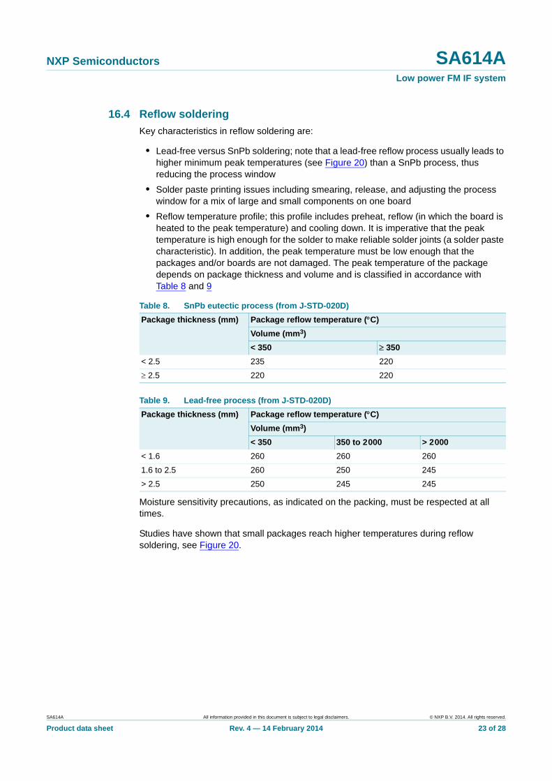
16.4 Reflow soldering
Key characteristics in reflow soldering are:
• Lead-free versus SnPb soldering; note that a lead-free reflow process usually leads to higher minimum peak temperatures (see Figure 20) than a SnPb process, thus reducing the process window
• Solder paste printing issues including smearing, release, and adjusting the process window for a mix of large and small components on one board
• Reflow temperature profile; this profile includes preheat, reflow (in which the board is heated to the peak temperature) and cooling down. It is imperative that the peak temperature is high enough for the solder to make reliable solder joints (a solder paste characteristic). In addition, the peak temperature must be low enough that the packages and/or boards are not damaged. The peak temperature of the package depends on package thickness and volume and is classified in accordance with Table 8 and 9
Moisture sensitivity precautions, as indicated on the packing, must be respected at all times.
Studies have shown that small packages reach higher temperatures during reflow soldering, see Figure 20.
Table 8. SnPb eutectic process (from J-STD-020D)
Package thickness (mm) Package reflow temperature (C)
Volume (mm3)
< 350 350
< 2.5 235 220
2.5 220 220
Table 9. Lead-free process (from J-STD-020D)
Package thickness (mm) Package reflow temperature (C)
Volume (mm3)
< 350 350 to 2000 > 2000
< 1.6 260 260 260
1.6 to 2.5 260 250 245
> 2.5 250 245 245
SA614A All information provided in this document is subject to legal disclaimers. © NXP B.V. 2014. All rights reserved.
Product data sheet Rev. 4 — 14 February 2014 23 of 28

NXP Semiconductors SA614ALow power FM IF system
For further information on temperature profiles, refer to Application Note AN10365 “Surface mount reflow soldering description”.
17. Abbreviations
MSL: Moisture Sensitivity Level
Fig 20. Temperature profiles for large and small components
001aac844
temperature
time
minimum peak temperature= minimum soldering temperature
maximum peak temperature= MSL limit, damage level
peak temperature
Table 10. Abbreviations
Acronym Description
AM Amplitude Modulation
ASK Amplitude Shift Keying
FM Frequency Modulation
FSK Frequency Shift Keying
IF Intermediate Frequency
PCB Printed-Circuit Board
RF Radio Frequency
RSSI Received Signal Strength Indicator
SINAD Signal-to-Noise And Distortion ratio
SA614A All information provided in this document is subject to legal disclaimers. © NXP B.V. 2014. All rights reserved.
Product data sheet Rev. 4 — 14 February 2014 24 of 28

NXP Semiconductors SA614ALow power FM IF system
18. Revision history
Table 11. Revision history
Document ID Release date Data sheet status Change notice Supersedes
SA614A v.4 20140214 Product data sheet - SA614A v.3
Modifications: • The format of this document has been redesigned to comply with the new identity guidelines of NXP Semiconductors.
• Legal texts have been adapted to the new company name where appropriate.
• Added type number SA614AHR.
SA614A v.3 19971107 Product specification - SA614A v.2
SA614A v.2 19971107 Product specification - SA614A v.1
SA614A v.1 19941215 Product specification - -
SA614A All information provided in this document is subject to legal disclaimers. © NXP B.V. 2014. All rights reserved.
Product data sheet Rev. 4 — 14 February 2014 25 of 28

NXP Semiconductors SA614ALow power FM IF system
19. Legal information
19.1 Data sheet status
[1] Please consult the most recently issued document before initiating or completing a design.
[2] The term ‘short data sheet’ is explained in section “Definitions”.
[3] The product status of device(s) described in this document may have changed since this document was published and may differ in case of multiple devices. The latest product status information is available on the Internet at URL http://www.nxp.com.
19.2 Definitions
Draft — The document is a draft version only. The content is still under internal review and subject to formal approval, which may result in modifications or additions. NXP Semiconductors does not give any representations or warranties as to the accuracy or completeness of information included herein and shall have no liability for the consequences of use of such information.
Short data sheet — A short data sheet is an extract from a full data sheet with the same product type number(s) and title. A short data sheet is intended for quick reference only and should not be relied upon to contain detailed and full information. For detailed and full information see the relevant full data sheet, which is available on request via the local NXP Semiconductors sales office. In case of any inconsistency or conflict with the short data sheet, the full data sheet shall prevail.
Product specification — The information and data provided in a Product data sheet shall define the specification of the product as agreed between NXP Semiconductors and its customer, unless NXP Semiconductors and customer have explicitly agreed otherwise in writing. In no event however, shall an agreement be valid in which the NXP Semiconductors product is deemed to offer functions and qualities beyond those described in the Product data sheet.
19.3 Disclaimers
Limited warranty and liability — Information in this document is believed to be accurate and reliable. However, NXP Semiconductors does not give any representations or warranties, expressed or implied, as to the accuracy or completeness of such information and shall have no liability for the consequences of use of such information. NXP Semiconductors takes no responsibility for the content in this document if provided by an information source outside of NXP Semiconductors.
In no event shall NXP Semiconductors be liable for any indirect, incidental, punitive, special or consequential damages (including - without limitation - lost profits, lost savings, business interruption, costs related to the removal or replacement of any products or rework charges) whether or not such damages are based on tort (including negligence), warranty, breach of contract or any other legal theory.
Notwithstanding any damages that customer might incur for any reason whatsoever, NXP Semiconductors’ aggregate and cumulative liability towards customer for the products described herein shall be limited in accordance with the Terms and conditions of commercial sale of NXP Semiconductors.
Right to make changes — NXP Semiconductors reserves the right to make changes to information published in this document, including without limitation specifications and product descriptions, at any time and without notice. This document supersedes and replaces all information supplied prior to the publication hereof.
Suitability for use — NXP Semiconductors products are not designed, authorized or warranted to be suitable for use in life support, life-critical or safety-critical systems or equipment, nor in applications where failure or malfunction of an NXP Semiconductors product can reasonably be expected to result in personal injury, death or severe property or environmental damage. NXP Semiconductors and its suppliers accept no liability for inclusion and/or use of NXP Semiconductors products in such equipment or applications and therefore such inclusion and/or use is at the customer’s own risk.
Applications — Applications that are described herein for any of these products are for illustrative purposes only. NXP Semiconductors makes no representation or warranty that such applications will be suitable for the specified use without further testing or modification.
Customers are responsible for the design and operation of their applications and products using NXP Semiconductors products, and NXP Semiconductors accepts no liability for any assistance with applications or customer product design. It is customer’s sole responsibility to determine whether the NXP Semiconductors product is suitable and fit for the customer’s applications and products planned, as well as for the planned application and use of customer’s third party customer(s). Customers should provide appropriate design and operating safeguards to minimize the risks associated with their applications and products.
NXP Semiconductors does not accept any liability related to any default, damage, costs or problem which is based on any weakness or default in the customer’s applications or products, or the application or use by customer’s third party customer(s). Customer is responsible for doing all necessary testing for the customer’s applications and products using NXP Semiconductors products in order to avoid a default of the applications and the products or of the application or use by customer’s third party customer(s). NXP does not accept any liability in this respect.
Limiting values — Stress above one or more limiting values (as defined in the Absolute Maximum Ratings System of IEC 60134) will cause permanent damage to the device. Limiting values are stress ratings only and (proper) operation of the device at these or any other conditions above those given in the Recommended operating conditions section (if present) or the Characteristics sections of this document is not warranted. Constant or repeated exposure to limiting values will permanently and irreversibly affect the quality and reliability of the device.
Terms and conditions of commercial sale — NXP Semiconductors products are sold subject to the general terms and conditions of commercial sale, as published at http://www.nxp.com/profile/terms, unless otherwise agreed in a valid written individual agreement. In case an individual agreement is concluded only the terms and conditions of the respective agreement shall apply. NXP Semiconductors hereby expressly objects to applying the customer’s general terms and conditions with regard to the purchase of NXP Semiconductors products by customer.
No offer to sell or license — Nothing in this document may be interpreted or construed as an offer to sell products that is open for acceptance or the grant, conveyance or implication of any license under any copyrights, patents or other industrial or intellectual property rights.
Document status[1][2] Product status[3] Definition
Objective [short] data sheet Development This document contains data from the objective specification for product development.
Preliminary [short] data sheet Qualification This document contains data from the preliminary specification.
Product [short] data sheet Production This document contains the product specification.
SA614A All information provided in this document is subject to legal disclaimers. © NXP B.V. 2014. All rights reserved.
Product data sheet Rev. 4 — 14 February 2014 26 of 28

NXP Semiconductors SA614ALow power FM IF system
Export control — This document as well as the item(s) described herein may be subject to export control regulations. Export might require a prior authorization from competent authorities.
Non-automotive qualified products — Unless this data sheet expressly states that this specific NXP Semiconductors product is automotive qualified, the product is not suitable for automotive use. It is neither qualified nor tested in accordance with automotive testing or application requirements. NXP Semiconductors accepts no liability for inclusion and/or use of non-automotive qualified products in automotive equipment or applications.
In the event that customer uses the product for design-in and use in automotive applications to automotive specifications and standards, customer (a) shall use the product without NXP Semiconductors’ warranty of the product for such automotive applications, use and specifications, and (b) whenever customer uses the product for automotive applications beyond
NXP Semiconductors’ specifications such use shall be solely at customer’s own risk, and (c) customer fully indemnifies NXP Semiconductors for any liability, damages or failed product claims resulting from customer design and use of the product for automotive applications beyond NXP Semiconductors’ standard warranty and NXP Semiconductors’ product specifications.
Translations — A non-English (translated) version of a document is for reference only. The English version shall prevail in case of any discrepancy between the translated and English versions.
19.4 TrademarksNotice: All referenced brands, product names, service names and trademarks are the property of their respective owners.
20. Contact information
For more information, please visit: http://www.nxp.com
For sales office addresses, please send an email to: [email protected]
SA614A All information provided in this document is subject to legal disclaimers. © NXP B.V. 2014. All rights reserved.
Product data sheet Rev. 4 — 14 February 2014 27 of 28

NXP Semiconductors SA614ALow power FM IF system
21. Contents
1 General description . . . . . . . . . . . . . . . . . . . . . . 1
2 Features and benefits . . . . . . . . . . . . . . . . . . . . 1
3 Applications . . . . . . . . . . . . . . . . . . . . . . . . . . . . 1
4 Ordering information. . . . . . . . . . . . . . . . . . . . . 1
5 Block diagram . . . . . . . . . . . . . . . . . . . . . . . . . . 2
6 Pinning information. . . . . . . . . . . . . . . . . . . . . . 36.1 Pinning . . . . . . . . . . . . . . . . . . . . . . . . . . . . . . . 36.2 Pin description . . . . . . . . . . . . . . . . . . . . . . . . . 4
7 Functional description . . . . . . . . . . . . . . . . . . . 5
8 Limiting values. . . . . . . . . . . . . . . . . . . . . . . . . . 6
9 Thermal characteristics . . . . . . . . . . . . . . . . . . 6
10 Static characteristics. . . . . . . . . . . . . . . . . . . . . 6
11 Dynamic characteristics . . . . . . . . . . . . . . . . . . 7
12 Performance curves . . . . . . . . . . . . . . . . . . . . . 8
13 Application information. . . . . . . . . . . . . . . . . . . 913.1 Circuit description . . . . . . . . . . . . . . . . . . . . . . 1013.2 IF amplifiers . . . . . . . . . . . . . . . . . . . . . . . . . . 1113.3 Stability considerations . . . . . . . . . . . . . . . . . 1313.4 Quadrature detector . . . . . . . . . . . . . . . . . . . . 1413.5 Frequency discriminator design equations . . . 1513.6 Audio outputs . . . . . . . . . . . . . . . . . . . . . . . . . 1613.7 RSSI . . . . . . . . . . . . . . . . . . . . . . . . . . . . . . . . 1713.8 Additional circuitry . . . . . . . . . . . . . . . . . . . . . 17
14 Test information. . . . . . . . . . . . . . . . . . . . . . . . 18
15 Package outline . . . . . . . . . . . . . . . . . . . . . . . . 20
16 Soldering of SMD packages . . . . . . . . . . . . . . 2216.1 Introduction to soldering . . . . . . . . . . . . . . . . . 2216.2 Wave and reflow soldering . . . . . . . . . . . . . . . 2216.3 Wave soldering . . . . . . . . . . . . . . . . . . . . . . . . 2216.4 Reflow soldering . . . . . . . . . . . . . . . . . . . . . . . 23
17 Abbreviations. . . . . . . . . . . . . . . . . . . . . . . . . . 24
18 Revision history. . . . . . . . . . . . . . . . . . . . . . . . 25
19 Legal information. . . . . . . . . . . . . . . . . . . . . . . 2619.1 Data sheet status . . . . . . . . . . . . . . . . . . . . . . 2619.2 Definitions. . . . . . . . . . . . . . . . . . . . . . . . . . . . 2619.3 Disclaimers . . . . . . . . . . . . . . . . . . . . . . . . . . . 2619.4 Trademarks. . . . . . . . . . . . . . . . . . . . . . . . . . . 27
20 Contact information. . . . . . . . . . . . . . . . . . . . . 27
21 Contents . . . . . . . . . . . . . . . . . . . . . . . . . . . . . . 28
© NXP B.V. 2014. All rights reserved.
For more information, please visit: http://www.nxp.comFor sales office addresses, please send an email to: [email protected]
Date of release: 14 February 2014
Document identifier: SA614A
Please be aware that important notices concerning this document and the product(s)described herein, have been included in section ‘Legal information’.