S32K14x Series Cookbook - NXP Semiconductors · S32K14x Series Cookbook, Rev. 1, August 2017...
68
NXP Semiconductors Application Note Document Number: AN5413 Rev. 1, 08/2017 Contents 1 Introduction This application note provides software examples and describes necessary startup steps needed to help users get started with S32K14x series MCUs. Complete source code and projects are available in a separate zip file at nxp.com. Projects are implemented using NXP’s S32 Design Studio v 1.3 and tested on the S32K144 evaluation board version S32K144EVB-Q100. To access the projects in the zip file, either: • Windows: unzip archive file to a folder • S32 Design Studio: use File - Import and select the zip file. These examples and others are also ported to ARM(R) Keil TM MDK tools. See ARMKeil Application Note 304 at http://www.keil.com/appnotes/docs/apnt_304.asp for further information. 1 Introduction . . . . . . . . . . . . . . . . . . . . . . . . . . . . . . . . . . . 1 2 Software examples . . . . . . . . . . . . . . . . . . . . . . . . . . . . . 2 2.1 Hello World . . . . . . . . . . . . . . . . . . . . . . . . . . . . . . . 4 2.2 Hello World + Clocks . . . . . . . . . . . . . . . . . . . . . . . . 6 2.3 Hello World + Interrupts. . . . . . . . . . . . . . . . . . . . . 11 2.4 DMA . . . . . . . . . . . . . . . . . . . . . . . . . . . . . . . . . . . 16 2.5 Timed I/O (FTM) . . . . . . . . . . . . . . . . . . . . . . . . . . 22 2.6 ADC - SW Trigger . . . . . . . . . . . . . . . . . . . . . . . . . 28 2.7 UART. . . . . . . . . . . . . . . . . . . . . . . . . . . . . . . . . . . 33 2.8 SPI . . . . . . . . . . . . . . . . . . . . . . . . . . . . . . . . . . . . . 38 2.9 CAN 2.0 . . . . . . . . . . . . . . . . . . . . . . . . . . . . . . . . . 43 2.10 CAN FD . . . . . . . . . . . . . . . . . . . . . . . . . . . . . . . . . 53 3 Startup code . . . . . . . . . . . . . . . . . . . . . . . . . . . . . . . . . 65 3.1 S32 Design Studio, S32K14x flash target . . . . . . . 65 4 Header files cheat sheet . . . . . . . . . . . . . . . . . . . . . . . . 66 5 Adding projects . . . . . . . . . . . . . . . . . . . . . . . . . . . . . . . 67 6 Revision history . . . . . . . . . . . . . . . . . . . . . . . . . . . . . . . 68 S32K14x Series Cookbook Software examples and startup code to exercise microcontroller features
Transcript of S32K14x Series Cookbook - NXP Semiconductors · S32K14x Series Cookbook, Rev. 1, August 2017...

NXP SemiconductorsApplication Note
Document Number: AN5413Rev. 1, 08/2017
ContentsIntroduction . . . . . . . . . . . . . . . . . . . . . . . . . . . . . . . . . . . 1Software examples . . . . . . . . . . . . . . . . . . . . . . . . . . . . . 2
2.1 Hello World . . . . . . . . . . . . . . . . . . . . . . . . . . . . . . . 42.2 Hello World + Clocks . . . . . . . . . . . . . . . . . . . . . . . . 62.3 Hello World + Interrupts. . . . . . . . . . . . . . . . . . . . . 112.4 DMA . . . . . . . . . . . . . . . . . . . . . . . . . . . . . . . . . . . 162.5 Timed I/O (FTM) . . . . . . . . . . . . . . . . . . . . . . . . . . 222.6 ADC - SW Trigger . . . . . . . . . . . . . . . . . . . . . . . . . 282.7 UART. . . . . . . . . . . . . . . . . . . . . . . . . . . . . . . . . . . 332.8 SPI. . . . . . . . . . . . . . . . . . . . . . . . . . . . . . . . . . . . . 382.9 CAN 2.0. . . . . . . . . . . . . . . . . . . . . . . . . . . . . . . . . 432.10 CAN FD . . . . . . . . . . . . . . . . . . . . . . . . . . . . . . . . . 53Startup code . . . . . . . . . . . . . . . . . . . . . . . . . . . . . . . . . 65
3.1 S32 Design Studio, S32K14x flash target . . . . . . . 65Header files cheat sheet . . . . . . . . . . . . . . . . . . . . . . . . 66Adding projects . . . . . . . . . . . . . . . . . . . . . . . . . . . . . . . 67Revision history . . . . . . . . . . . . . . . . . . . . . . . . . . . . . . . 68
S32K14x Series Cookbook Software examples and startup code to exercise microcontroller features
1 IntroductionThis application note provides software examples and describes necessary startup steps needed to help users get started with S32K14x series MCUs.
Complete source code and projects are available in a separate zip file at nxp.com. Projects are implemented using NXP’s S32 Design Studio v 1.3 and tested on the S32K144 evaluation board version S32K144EVB-Q100. To access the projects in the zip file, either:
• Windows: unzip archive file to a folder
• S32 Design Studio: use File - Import and select the zip file.
These examples and others are also ported to ARM(R) KeilTM MDK tools. See ARMKeil Application Note 304 at http://www.keil.com/appnotes/docs/apnt_304.asp for further information.
12
3
456

Software examples
2 Software examplesThe table below lists the examples in this application note. The three Hello World examples are intended to be base projects that can be copied and code added to create a new project.
Table 1. List of examples
Example Programs Summary
Hello World hello Simplest project: • Configure GPIO • Output to LED follows switch input
Hello World + Clocks hello_clocks Perform common initialization for clocks and LPIT: • Initialize System Oscillator (SOSC) for 8 MHz crystal • Initialize SPLL with 8 MHz SOSC input to provide 80 MHz clock • Change Normal RUN mode clock from default FIRC to 160 MHz SPLL
(before dividers) • Initialize LPIT channel to count 40M clocks (1 second timeout) • Toggle output to LED every LPIT timeout
Hello World + Clocks + Interrupts
hello_clocks_interrupts The Hello World + Clock example is modified to service the PIT channel timeout with an interrupt service route: • Initialize system clock to 80 MHz • Initialize an LPIT channel for 1 second timeout and enable its interrupt • Wait forever • At LPIT timeout interrupt, toggle output to LED
DMA eDMA Transfer a string of bytes to a single byte location: • Initialize a Transfer Control Descriptor (TCD) • Use software (instead of peripheral DMA requests) to initiate transfers
Timed I/O (FTM) FTM Perform common timed I/O functions with FTM: • Module counter initialization • Pulse Width MOdulation • Output Compare • Input Capture
ADC - SW Trigger ADC Perform simple analog to digital conversions using software trigger: • Initialize ADC for SW trigger, continuous mode • Loop:
- Convert channel connected to pot on evaluation board- Scale result to 0 to 5000 mV- Light evaluation board LEDs to reflect voltage level- Convert channel connected to the ADC high reference voltage
UART UART Transmit and receive characters: • Initialize UART for 9600 baud, 1 stop, no parity • Loop:
- Transmit string, then a prompt character on new line- When character is received, echo it back
SPI LPSPI Transmit and receive a SPI frame: • Initialize LPSPI for 1M Baud, PCS3 which is connected to SPC on EVB • Wait for Tx FIFO to have at least one available slot then issue transmit • Wait for Rx FIFO to have at least one received frame then read data
S32K14x Series Cookbook, Rev. 1, August 2017
NXP Semiconductors2
Software examples
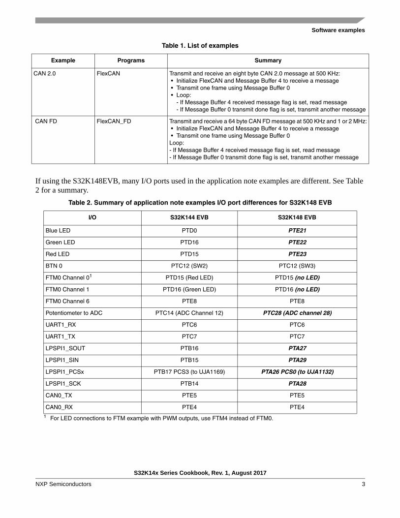
If using the S32K148EVB, many I/O ports used in the application note examples are different. See Table 2 for a summary.
CAN 2.0 FlexCAN Transmit and receive an eight byte CAN 2.0 message at 500 KHz: • Initialize FlexCAN and Message Buffer 4 to receive a message • Transmit one frame using Message Buffer 0 • Loop:
- If Message Buffer 4 received message flag is set, read message- If Message Buffer 0 transmit done flag is set, transmit another message
CAN FD FlexCAN_FD Transmit and receive a 64 byte CAN FD message at 500 KHz and 1 or 2 MHz: • Initialize FlexCAN and Message Buffer 4 to receive a message • Transmit one frame using Message Buffer 0Loop:- If Message Buffer 4 received message flag is set, read message- If Message Buffer 0 transmit done flag is set, transmit another message
Table 2. Summary of application note examples I/O port differences for S32K148 EVB
I/O S32K144 EVB S32K148 EVB
Blue LED PTD0 PTE21
Green LED PTD16 PTE22
Red LED PTD15 PTE23
BTN 0 PTC12 (SW2) PTC12 (SW3)
FTM0 Channel 01
1 For LED connections to FTM example with PWM outputs, use FTM4 instead of FTM0.
PTD15 (Red LED) PTD15 (no LED)
FTM0 Channel 1 PTD16 (Green LED) PTD16 (no LED)
FTM0 Channel 6 PTE8 PTE8
Potentiometer to ADC PTC14 (ADC Channel 12) PTC28 (ADC channel 28)
UART1_RX PTC6 PTC6
UART1_TX PTC7 PTC7
LPSPI1_SOUT PTB16 PTA27
LPSPI1_SIN PTB15 PTA29
LPSPI1_PCSx PTB17 PCS3 (to UJA1169) PTA26 PCS0 (to UJA1132)
LPSPI1_SCK PTB14 PTA28
CAN0_TX PTE5 PTE5
CAN0_RX PTE4 PTE4
Table 1. List of examples
Example Programs Summary
S32K14x Series Cookbook, Rev. 1, August 2017
NXP Semiconductors 3
Software examples
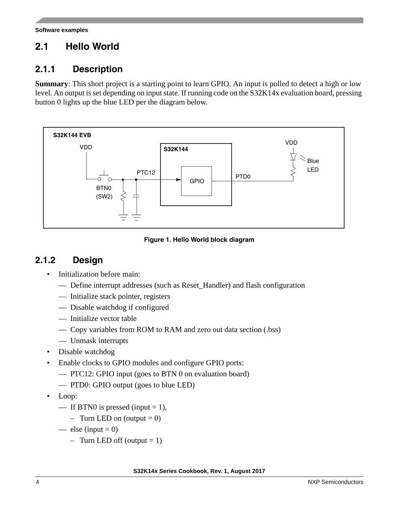
2.1 Hello World
2.1.1 Description
Summary: This short project is a starting point to learn GPIO. An input is polled to detect a high or low level. An output is set depending on input state. If running code on the S32K14x evaluation board, pressing button 0 lights up the blue LED per the diagram below.
Figure 1. Hello World block diagram
2.1.2 Design • Initialization before main:
— Define interrupt addresses (such as Reset_Handler) and flash configuration
— Initialize stack pointer, registers
— Disable watchdog if configured
— Initialize vector table
— Copy variables from ROM to RAM and zero out data section (.bss)
— Unmask interrupts
• Disable watchdog
• Enable clocks to GPIO modules and configure GPIO ports:
— PTC12: GPIO input (goes to BTN 0 on evaluation board)
— PTD0: GPIO output (goes to blue LED)
• Loop:
— If BTN0 is pressed (input = 1),
– Turn LED on (output = 0)
— else (input = 0)
– Turn LED off (output = 1)
PTD0
S32K144
GPIO
PTC12
BTN0
VDDVDD
Blue
(SW2)
LED
S32K144 EVB
S32K14x Series Cookbook, Rev. 1, August 2017
NXP Semiconductors4
Software examples
2.1.3 Code
2.1.3.1 hello.c
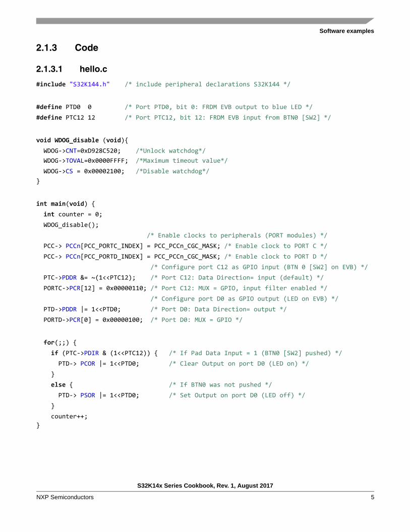
#include "S32K144.h" /* include peripheral declarations S32K144 */
#define PTD0 0 /* Port PTD0, bit 0: FRDM EVB output to blue LED */#define PTC12 12 /* Port PTC12, bit 12: FRDM EVB input from BTN0 [SW2] */
void WDOG_disable (void){ WDOG->CNT=0xD928C520; /*Unlock watchdog*/ WDOG->TOVAL=0x0000FFFF; /*Maximum timeout value*/ WDOG->CS = 0x00002100; /*Disable watchdog*/}
int main(void) { int counter = 0; WDOG_disable(); /* Enable clocks to peripherals (PORT modules) */ PCC-> PCCn[PCC_PORTC_INDEX] = PCC_PCCn_CGC_MASK; /* Enable clock to PORT C */ PCC-> PCCn[PCC_PORTD_INDEX] = PCC_PCCn_CGC_MASK; /* Enable clock to PORT D */ /* Configure port C12 as GPIO input (BTN 0 [SW2] on EVB) */ PTC->PDDR &= ~(1<<PTC12); /* Port C12: Data Direction= input (default) */ PORTC->PCR[12] = 0x00000110; /* Port C12: MUX = GPIO, input filter enabled */ /* Configure port D0 as GPIO output (LED on EVB) */ PTD->PDDR |= 1<<PTD0; /* Port D0: Data Direction= output */ PORTD->PCR[0] = 0x00000100; /* Port D0: MUX = GPIO */
for(;;) { if (PTC->PDIR & (1<<PTC12)) { /* If Pad Data Input = 1 (BTN0 [SW2] pushed) */ PTD-> PCOR |= 1<<PTD0; /* Clear Output on port D0 (LED on) */ } else { /* If BTN0 was not pushed */ PTD-> PSOR |= 1<<PTD0; /* Set Output on port D0 (LED off) */ } counter++;}
S32K14x Series Cookbook, Rev. 1, August 2017
NXP Semiconductors 5

Software examples
2.2 Hello World + Clocks
2.2.1 Description
Summary: This project provides common initialization for clocks and an LPIT channel counter function. Core clock is set to 80 MHz. LPIT0 channel 0 is configured to count one second of SPLL clocks. Software polls the channel’s timeout flag and toggles the GPIO output to the LED when the flag sets.
Figure 2. Hello World + Clocks block diagram
PTD0
S32K144
OSCXTAL
8 MHz
SOSC_CLKPLL
FIRC
SIRC
48 MHz
FIRC_CLK
SIRC_CLK
8 MHz
CORE_CLK, SYSCLK (80 MHz)
BUS_CLK (40 MHz)
FLASH_CLK,
SCG_SLOW_CLK
SPLL_CLK (160 MHz)
SPLL_DIV2_CLK LPIT0Chan 0
.
.
GPIO(to
SOSC_DIV1_CLK (8 MHz)SOSC_DIV2_CLK (8 MHz)
Software polling
controls GPIO
S32K144 EVB
SCG_
SPLL_DIV1_CLK (80 MHz)SPLL_DIV2_CLK (40 MHz)
(40 MHz)
LED)FIRC_DIV2_CLK SIRC_DIV2_CLK SOSC_DIV2_CLK
Functionalclock(40 MHz)
Moduleclock(BUS_CLK,40 MHz)
SOSCDIV
SCG_SPLLDIV
SCG_RCCR
SCG_RCCR
SCG_RCCR
(26 2/3 MHz)
SCG_RCCR[SCS]
(1 sec)
S32K14x Series Cookbook, Rev. 1, August 2017
NXP Semiconductors6
Software examples
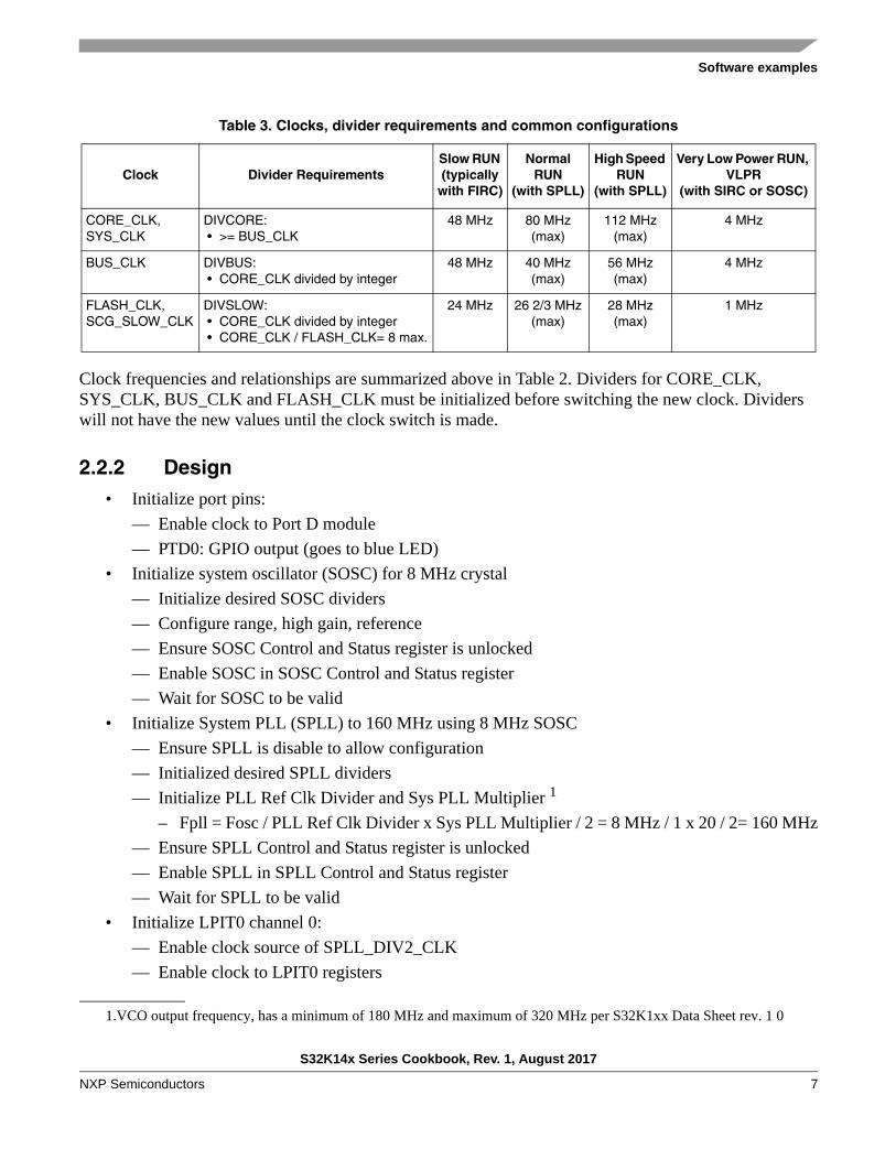
Clock frequencies and relationships are summarized above in Table 2. Dividers for CORE_CLK, SYS_CLK, BUS_CLK and FLASH_CLK must be initialized before switching the new clock. Dividers will not have the new values until the clock switch is made.
2.2.2 Design • Initialize port pins:
— Enable clock to Port D module
— PTD0: GPIO output (goes to blue LED)
• Initialize system oscillator (SOSC) for 8 MHz crystal
— Initialize desired SOSC dividers
— Configure range, high gain, reference
— Ensure SOSC Control and Status register is unlocked
— Enable SOSC in SOSC Control and Status register
— Wait for SOSC to be valid
• Initialize System PLL (SPLL) to 160 MHz using 8 MHz SOSC
— Ensure SPLL is disable to allow configuration
— Initialized desired SPLL dividers
— Initialize PLL Ref Clk Divider and Sys PLL Multiplier 1
– Fpll = Fosc / PLL Ref Clk Divider x Sys PLL Multiplier / 2 = 8 MHz / 1 x 20 / 2= 160 MHz
— Ensure SPLL Control and Status register is unlocked
— Enable SPLL in SPLL Control and Status register
— Wait for SPLL to be valid
• Initialize LPIT0 channel 0:
— Enable clock source of SPLL_DIV2_CLK
— Enable clock to LPIT0 registers
Table 3. Clocks, divider requirements and common configurations
Clock Divider RequirementsSlow RUN (typically
with FIRC)
Normal RUN
(with SPLL)
High Speed RUN
(with SPLL)
Very Low Power RUN, VLPR
(with SIRC or SOSC)
CORE_CLK,SYS_CLK
DIVCORE: • >= BUS_CLK
48 MHz 80 MHz(max)
112 MHz(max)
4 MHz
BUS_CLK DIVBUS: • CORE_CLK divided by integer
48 MHz 40 MHz(max)
56 MHz(max)
4 MHz
FLASH_CLK, SCG_SLOW_CLK
DIVSLOW: • CORE_CLK divided by integer • CORE_CLK / FLASH_CLK= 8 max.
24 MHz 26 2/3 MHz(max)
28 MHz(max)
1 MHz
1.VCO output frequency, has a minimum of 180 MHz and maximum of 320 MHz per S32K1xx Data Sheet rev. 1 0
S32K14x Series Cookbook, Rev. 1, August 2017
NXP Semiconductors 7
Software examples
— Enable LPIT0 module
— Initialize channel 0:
– Timeout = 1 second of clocks
– Set Mode to 32 bit counter and enable channel 0
• Change Normal RUN mode clock to SPLL
— Initialize clock dividers for CORE, BUS and FLASH for new target clock frequency
— Switch system clock input to SPLL (160 MHz before dividers)
• Loop:
— Wait for LPIT0 channel 0 flag
— Increment counter, toggle PTD0 GPIO output and clear channel flag
2.2.3 Code
2.2.3.1 hello_clocks.c
#include "S32K144.h" /* include peripheral declarations S32K144 */#include "clocks_and_modes.h" int lpit0_ch0_flag_counter = 0; /* LPIT0 timeout counter */
void PORT_init (void) { PCC-> PCCn[PCC_PORTD_INDEX] = PCC_PCCn_CGC_MASK; /* Enable clock for PORT D */ PTD->PDDR |= 1<<0; /* Port D0: Data Direction= output */ PORTD->PCR[0] = 0x00000100; /* Port D0: MUX = ALT1, GPIO (to blue LED on EVB) */}void LPIT0_init (void) { PCC->PCCn[PCC_LPIT_INDEX] = PCC_PCCn_PCS(6); /* Clock Src = 6 (SPLL2_DIV2_CLK)*/ PCC->PCCn[PCC_LPIT_INDEX] |= PCC_PCCn_CGC_MASK; /* Enable clk to LPIT0 regs */ LPIT0->MCR = 0x00000001; /* DBG_EN-0: Timer chans stop in Debug mode */ /* DOZE_EN=0: Timer chans are stopped in DOZE mode */ /* SW_RST=0: SW reset does not reset timer chans, regs */ /* M_CEN=1: enable module clk (allows writing other LPIT0 regs)*/ LPIT0->TMR[0].TVAL = 40000000; /* Chan 0 Timeout period: 40M clocks */ LPIT0->TMR[0].TCTRL = 0x00000001; /* T_EN=1: Timer channel is enabled */ /* CHAIN=0: channel chaining is disabled */ /* MODE=0: 32 periodic counter mode */ /* TSOT=0: Timer decrements immediately based on restart */ /* TSOI=0: Timer does not stop after timeout */ /* TROT=0 Timer will not reload on trigger */ /* TRG_SRC=0: External trigger source */ /* TRG_SEL=0: Timer chan 0 trigger source is selected*/}
S32K14x Series Cookbook, Rev. 1, August 2017
NXP Semiconductors8
Software examples
void WDOG_disable (void){ WDOG->CNT=0xD928C520; /*Unlock watchdog*/ WDOG->TOVAL=0x0000FFFF; /*Maximum timeout value*/ WDOG->CS = 0x00002100; /*Disable watchdog*/}
int main(void) { WDOG_disable(); PORT_init(); /* Configure ports */ SOSC_init_8MHz(); /* Initialize system oscillator for 8 MHz xtal */ SPLL_init_160MHz(); /* Initialize sysclk to 160 MHz with 8 MHz SOSC */ NormalRUNmode_80MHz(); /* Init clocks: 80 MHz sysclk & core, 40 MHz bus, 20 MHz flash */ LPIT0_init(); /* Initialize PIT0 for 1 second timeout */
for (;;) { /* Toggle output to LED every LPIT0 timeout */ while (0 == (LPIT0->MSR & LPIT_MSR_TIF0_MASK)) {} /* Wait for LPIT0 CH0 Flag */ lpit0_ch0_flag_counter++; /* Increment LPIT0 timeout counter */ PTD->PTOR |= 1<<0; /* Toggle output on port D0 (blue LED) */ LPIT0->MSR |= LPIT_MSR_TIF0_MASK; /* Clear LPIT0 timer flag 0 */}
S32K14x Series Cookbook, Rev. 1, August 2017
NXP Semiconductors 9

Software examples
2.2.3.2 clocks_and_modes.c
#include "S32K144.h" /* include peripheral declarations S32K144 */#include "clocks_and_modes.h"
void SOSC_init_8MHz(void) { SCG->SOSCDIV=0x00000101; /* SOSCDIV1 & SOSCDIV2 =1: divide by 1 */ SCG->SOSCCFG=0x00000024; /* Range=2: Medium freq (SOSC between 1MHz-8MHz)*/ /* HGO=0: Config xtal osc for low power */ /* EREFS=1: Input is external XTAL */ while(SCG->SOSCCSR & SCG_SOSCCSR_LK_MASK); /* Ensure SOSCCSR unlocked */ SCG->SOSCCSR=0x00000001; /* LK=0: SOSCCSR can be written */ /* SOSCCMRE=0: OSC CLK monitor IRQ if enabled */ /* SOSCCM=0: OSC CLK monitor disabled */ /* SOSCERCLKEN=0: Sys OSC 3V ERCLK output clk disabled */ /* SOSCLPEN=0: Sys OSC disabled in VLP modes */ /* SOSCSTEN=0: Sys OSC disabled in Stop modes */ /* SOSCEN=1: Enable oscillator */ while(!(SCG->SOSCCSR & SCG_SOSCCSR_SOSCVLD_MASK)); /* Wait for sys OSC clk valid */}void SPLL_init_160MHz(void) { while(SCG->SPLLCSR & SCG_SPLLCSR_LK_MASK); /* Ensure SPLLCSR unlocked */ SCG->SPLLCSR = 0x00000000; /* SPLLEN=0: SPLL is disabled (default) */ SCG->SPLLDIV = 0x00000302; /* SPLLDIV1 divide by 2; SPLLDIV2 divide by 4 */ SCG->SPLLCFG = 0x00180000; /* PREDIV=0: Divide SOSC_CLK by 0+1=1 */ /* MULT=24: Multiply sys pll by 4+24=40 */ /* SPLL_CLK = 8MHz / 1 * 40 / 2 = 160 MHz */ while(SCG->SPLLCSR & SCG_SPLLCSR_LK_MASK); /* Ensure SPLLCSR unlocked */ SCG->SPLLCSR = 0x00000001; /* LK=0: SPLLCSR can be written */ /* SPLLCMRE=0: SPLL CLK monitor IRQ if enabled */ /* SPLLCM=0: SPLL CLK monitor disabled */ /* SPLLSTEN=0: SPLL disabled in Stop modes */ /* SPLLEN=1: Enable SPLL */ while(!(SCG->SPLLCSR & SCG_SPLLCSR_SPLLVLD_MASK)); /* Wait for SPLL valid */}void NormalRUNmode_80MHz (void) { /* Change to normal RUN mode with 8MHz SOSC, 80 MHz PLL*/ SCG->RCCR=SCG_RCCR_SCS(6) /* PLL as clock source*/ |SCG_RCCR_DIVCORE(0b01) /* DIVCORE=1, div. by 2: Core clock = 160/2 MHz = 80 MHz*/ |SCG_RCCR_DIVBUS(0b01) /* DIVBUS=1, div. by 2: bus clock = 40 MHz*/ |SCG_RCCR_DIVSLOW(0b10); /* DIVSLOW=2, div. by 3: SCG slow, flash clock= 26 2/3 MHz*/ while (((SCG->CSR & SCG_CSR_SCS_MASK) >> SCG_CSR_SCS_SHIFT ) != 6) {} /* Wait for sys clk src = SPLL */}
S32K14x Series Cookbook, Rev. 1, August 2017
NXP Semiconductors10
Software examples
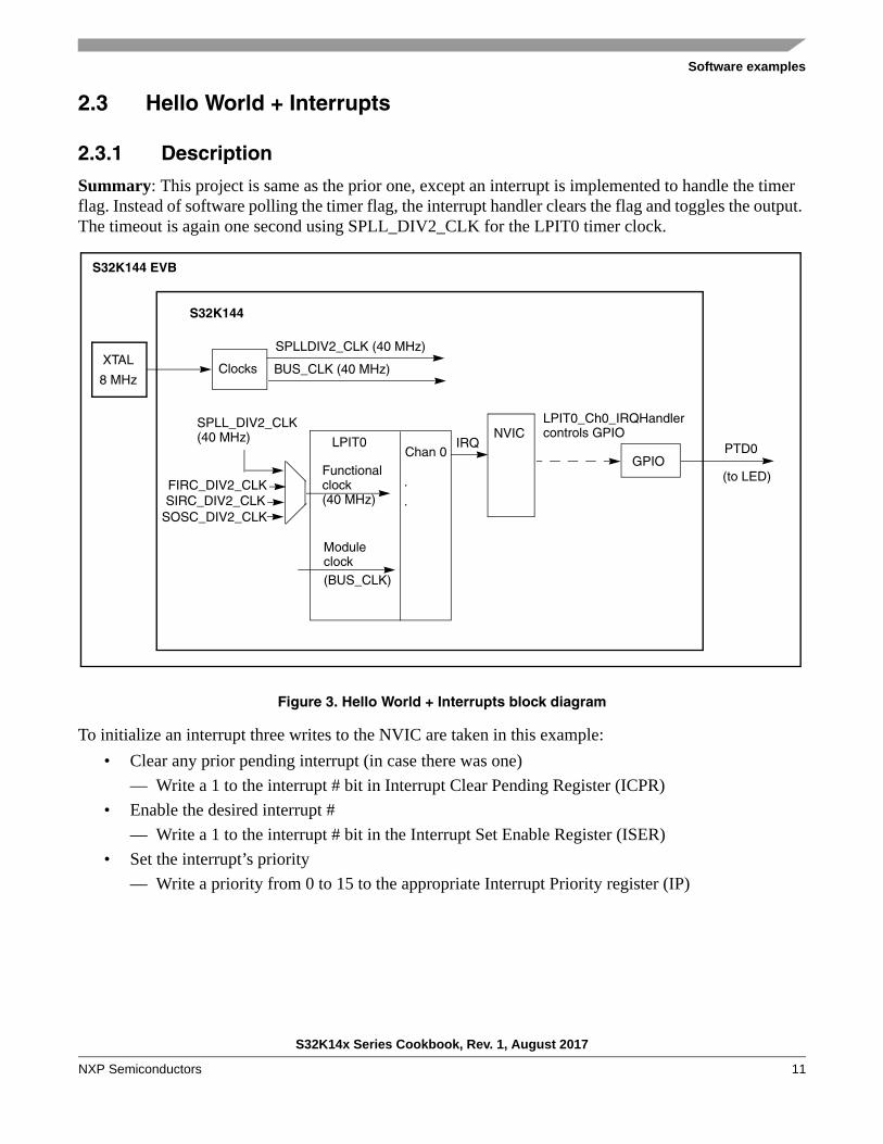
2.3 Hello World + Interrupts
2.3.1 Description
Summary: This project is same as the prior one, except an interrupt is implemented to handle the timer flag. Instead of software polling the timer flag, the interrupt handler clears the flag and toggles the output. The timeout is again one second using SPLL_DIV2_CLK for the LPIT0 timer clock.
Figure 3. Hello World + Interrupts block diagram
To initialize an interrupt three writes to the NVIC are taken in this example:
• Clear any prior pending interrupt (in case there was one)
— Write a 1 to the interrupt # bit in Interrupt Clear Pending Register (ICPR)
• Enable the desired interrupt #
— Write a 1 to the interrupt # bit in the Interrupt Set Enable Register (ISER)
• Set the interrupt’s priority
— Write a priority from 0 to 15 to the appropriate Interrupt Priority register (IP)
S32K144
ClocksXTAL
8 MHz
SPLLDIV2_CLK (40 MHz)
SPLL_DIV2_CLK
S32K144 EVB
PTD0LPIT0Chan 0
.
.
GPIO(to LED)
LPIT0_Ch0_IRQHandler
IRQNVIC controls GPIO(40 MHz)
Functionalclock(40 MHz)
Moduleclock(BUS_CLK)
BUS_CLK (40 MHz)
FIRC_DIV2_CLK SIRC_DIV2_CLK
SOSC_DIV2_CLK
S32K14x Series Cookbook, Rev. 1, August 2017
NXP Semiconductors 11
Software examples
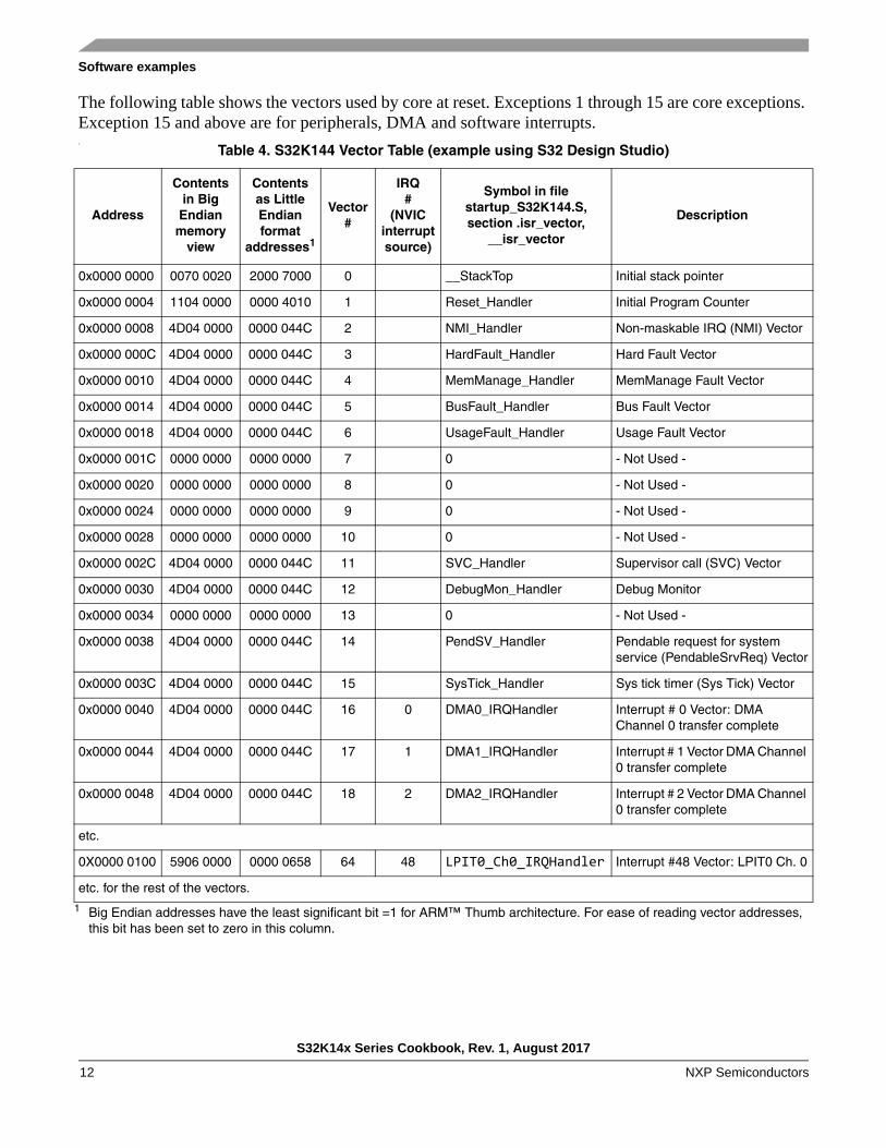
The following table shows the vectors used by core at reset. Exceptions 1 through 15 are core exceptions. Exception 15 and above are for peripherals, DMA and software interrupts.c
Table 4. S32K144 Vector Table (example using S32 Design Studio)
Address
Contents in Big
Endian memory
view
Contents as Little Endian format
addresses1
1 Big Endian addresses have the least significant bit =1 for ARM™ Thumb architecture. For ease of reading vector addresses, this bit has been set to zero in this column.
Vector#
IRQ #
(NVIC interrupt source)
Symbol in file startup_S32K144.S, section .isr_vector,
__isr_vector
Description
0x0000 0000 0070 0020 2000 7000 0 __StackTop Initial stack pointer
0x0000 0004 1104 0000 0000 4010 1 Reset_Handler Initial Program Counter
0x0000 0008 4D04 0000 0000 044C 2 NMI_Handler Non-maskable IRQ (NMI) Vector
0x0000 000C 4D04 0000 0000 044C 3 HardFault_Handler Hard Fault Vector
0x0000 0010 4D04 0000 0000 044C 4 MemManage_Handler MemManage Fault Vector
0x0000 0014 4D04 0000 0000 044C 5 BusFault_Handler Bus Fault Vector
0x0000 0018 4D04 0000 0000 044C 6 UsageFault_Handler Usage Fault Vector
0x0000 001C 0000 0000 0000 0000 7 0 - Not Used -
0x0000 0020 0000 0000 0000 0000 8 0 - Not Used -
0x0000 0024 0000 0000 0000 0000 9 0 - Not Used -
0x0000 0028 0000 0000 0000 0000 10 0 - Not Used -
0x0000 002C 4D04 0000 0000 044C 11 SVC_Handler Supervisor call (SVC) Vector
0x0000 0030 4D04 0000 0000 044C 12 DebugMon_Handler Debug Monitor
0x0000 0034 0000 0000 0000 0000 13 0 - Not Used -
0x0000 0038 4D04 0000 0000 044C 14 PendSV_Handler Pendable request for system service (PendableSrvReq) Vector
0x0000 003C 4D04 0000 0000 044C 15 SysTick_Handler Sys tick timer (Sys Tick) Vector
0x0000 0040 4D04 0000 0000 044C 16 0 DMA0_IRQHandler Interrupt # 0 Vector: DMA Channel 0 transfer complete
0x0000 0044 4D04 0000 0000 044C 17 1 DMA1_IRQHandler Interrupt # 1 Vector DMA Channel 0 transfer complete
0x0000 0048 4D04 0000 0000 044C 18 2 DMA2_IRQHandler Interrupt # 2 Vector DMA Channel 0 transfer complete
etc.
0X0000 0100 5906 0000 0000 0658 64 48 LPIT0_Ch0_IRQHandler Interrupt #48 Vector: LPIT0 Ch. 0
etc. for the rest of the vectors.
S32K14x Series Cookbook, Rev. 1, August 2017
NXP Semiconductors12
Software examples
2.3.2 Design • Initialize port pins:
— Enable clock to Port D module
— PTD0: GPIO output (goes to blue LED)
• Initialize system oscillator (SOSC) for 8 MHz crystal:
— Initialize desired SOSC dividers
— Configure range, high gain, reference
— Ensure SOSC Control and Status register is unlocked
— Enable SOSC in SOSC Control and Status register
— Wait for SOSC to be valid
• Initialize System PLL (SPLL) to 160 MHz using 8 MHz SOSC:
— Ensure SPLL is disable to allow configuration
— Initialized desired SPLL dividers
— Initialize PLL Ref Clk Divider and Sys PLL Multiplier 1
– Fpll = Fosc / PLL Ref Clk Divider x Sys PLL Multiplier / 2 = 8 MHz / 1 x 40 / 2= 160 MHz
— Ensure SPLL Control and Status register is unlocked
— Enable SPLL in SPLL Control and Status register
— Wait for SPLL to be valid
• Initialize LPIT0 channel 0:
— Enable clock source of SPLL_DIV2_CLK
— Enable clock to LPIT0 registers
— Enable LPIT0 module
— Initialize channel 0:
– Enable channel’s interrupt
– Timeout = 1 second of clocks
– Set Mode to 32 bit counter and enable channel 0
• Change Normal RUN mode clock to SPLL:
— Initialize clock dividers for CORE, BUS and FLASH for new target clock frequency
— Switch system clock input to SPLL (160 MHz before dividers)
• Loop: wait forever
• LPIT_0 Channel 0 Interrupt Handler:
— Clear channel flag2
— Increment counter
— Toggle PTD0 GPIO output
1.VCO output frequency, has a minimum of 180 MHz and maximum of 320 MHz per S32K1xx Data Sheet rev. 1 02.To ensure interrupt flag clears before routine exit, perform a memory read-after-write such as ctr++. Refererence:S32K14x Series Reference Manual, Rev. 1, 08/2016, section 3.4.1 and http://www.keil.com/support/docs/3928.htm
S32K14x Series Cookbook, Rev. 1, August 2017
NXP Semiconductors 13
Software examples
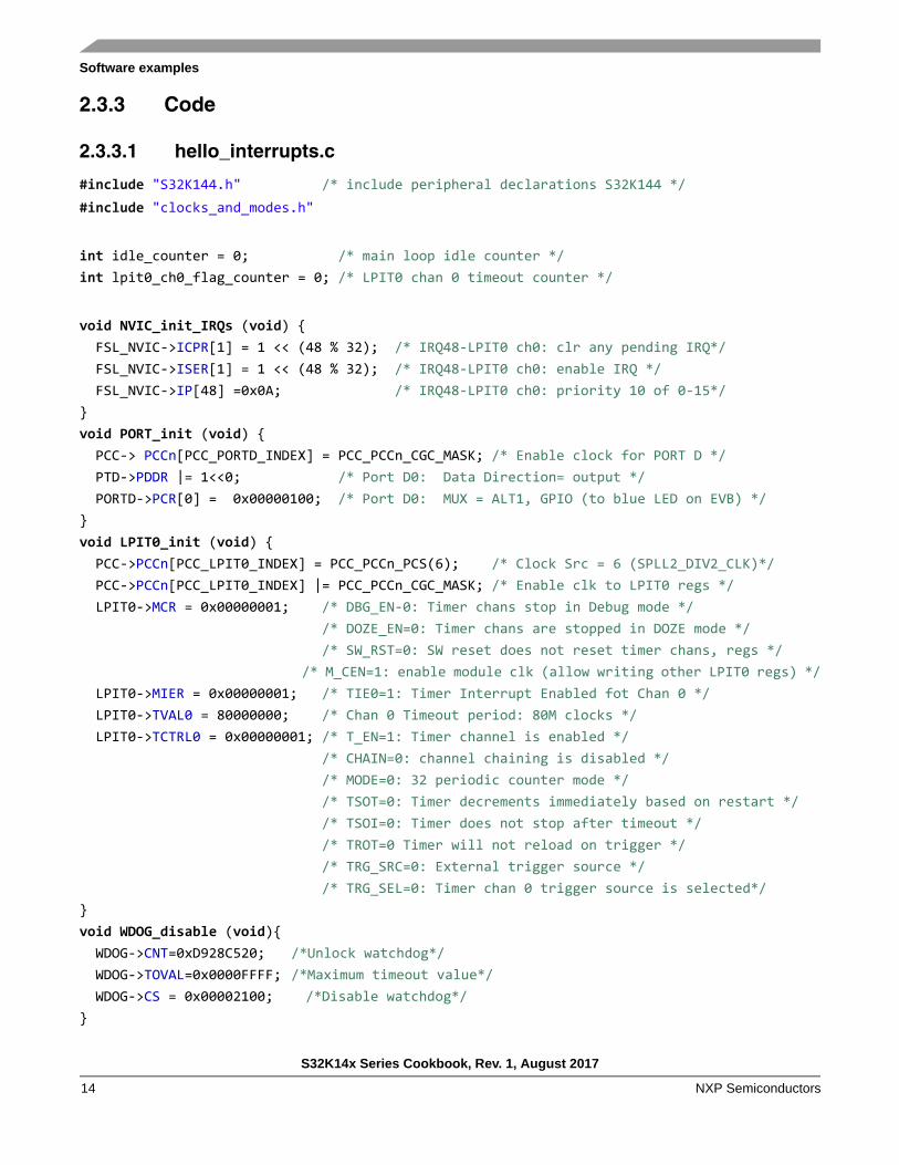
2.3.3 Code
2.3.3.1 hello_interrupts.c
#include "S32K144.h" /* include peripheral declarations S32K144 */#include "clocks_and_modes.h"
int idle_counter = 0; /* main loop idle counter */int lpit0_ch0_flag_counter = 0; /* LPIT0 chan 0 timeout counter */
void NVIC_init_IRQs (void) { FSL_NVIC->ICPR[1] = 1 << (48 % 32); /* IRQ48-LPIT0 ch0: clr any pending IRQ*/ FSL_NVIC->ISER[1] = 1 << (48 % 32); /* IRQ48-LPIT0 ch0: enable IRQ */ FSL_NVIC->IP[48] =0x0A; /* IRQ48-LPIT0 ch0: priority 10 of 0-15*/}void PORT_init (void) { PCC-> PCCn[PCC_PORTD_INDEX] = PCC_PCCn_CGC_MASK; /* Enable clock for PORT D */ PTD->PDDR |= 1<<0; /* Port D0: Data Direction= output */ PORTD->PCR[0] = 0x00000100; /* Port D0: MUX = ALT1, GPIO (to blue LED on EVB) */}void LPIT0_init (void) { PCC->PCCn[PCC_LPIT0_INDEX] = PCC_PCCn_PCS(6); /* Clock Src = 6 (SPLL2_DIV2_CLK)*/ PCC->PCCn[PCC_LPIT0_INDEX] |= PCC_PCCn_CGC_MASK; /* Enable clk to LPIT0 regs */ LPIT0->MCR = 0x00000001; /* DBG_EN-0: Timer chans stop in Debug mode */ /* DOZE_EN=0: Timer chans are stopped in DOZE mode */ /* SW_RST=0: SW reset does not reset timer chans, regs */ /* M_CEN=1: enable module clk (allow writing other LPIT0 regs) */ LPIT0->MIER = 0x00000001; /* TIE0=1: Timer Interrupt Enabled fot Chan 0 */ LPIT0->TVAL0 = 80000000; /* Chan 0 Timeout period: 80M clocks */ LPIT0->TCTRL0 = 0x00000001; /* T_EN=1: Timer channel is enabled */ /* CHAIN=0: channel chaining is disabled */ /* MODE=0: 32 periodic counter mode */ /* TSOT=0: Timer decrements immediately based on restart */ /* TSOI=0: Timer does not stop after timeout */ /* TROT=0 Timer will not reload on trigger */ /* TRG_SRC=0: External trigger source */ /* TRG_SEL=0: Timer chan 0 trigger source is selected*/}void WDOG_disable (void){ WDOG->CNT=0xD928C520; /*Unlock watchdog*/ WDOG->TOVAL=0x0000FFFF; /*Maximum timeout value*/ WDOG->CS = 0x00002100; /*Disable watchdog*/}
S32K14x Series Cookbook, Rev. 1, August 2017
NXP Semiconductors14
Software examples
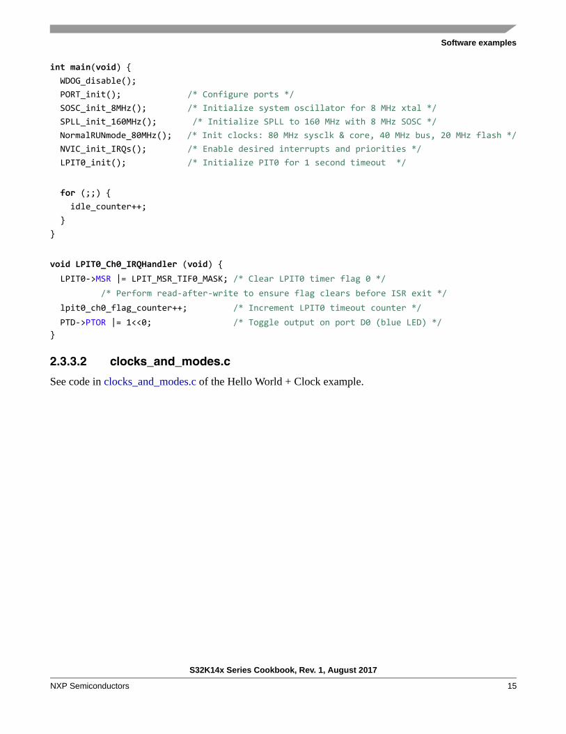
int main(void) { WDOG_disable(); PORT_init(); /* Configure ports */ SOSC_init_8MHz(); /* Initialize system oscillator for 8 MHz xtal */ SPLL_init_160MHz(); /* Initialize SPLL to 160 MHz with 8 MHz SOSC */ NormalRUNmode_80MHz(); /* Init clocks: 80 MHz sysclk & core, 40 MHz bus, 20 MHz flash */ NVIC_init_IRQs(); /* Enable desired interrupts and priorities */ LPIT0_init(); /* Initialize PIT0 for 1 second timeout */
for (;;) { idle_counter++; }}
void LPIT0_Ch0_IRQHandler (void) { LPIT0->MSR |= LPIT_MSR_TIF0_MASK; /* Clear LPIT0 timer flag 0 */ /* Perform read-after-write to ensure flag clears before ISR exit */ lpit0_ch0_flag_counter++; /* Increment LPIT0 timeout counter */ PTD->PTOR |= 1<<0; /* Toggle output on port D0 (blue LED) */}
2.3.3.2 clocks_and_modes.c
See code in clocks_and_modes.c of the Hello World + Clock example.
S32K14x Series Cookbook, Rev. 1, August 2017
NXP Semiconductors 15

Software examples
2.4 DMA
2.4.1 Description
Summary: Initialize an eDMA channel’s Transfer Control Descriptor (TCD) to transfer a string of bytes (“Hello world”) from an array in SRAM to a single SRAM byte location. This emulates a common use of DMA, where a string of data or commands is transferred automatically under DMA control to an input register of a peripheral. The intent of this example is to illustrate how to set up a DMA transfer.
Figure 4. DMA example block diagram
The DMA MUX is required when using DMA with peripherals. Peripheral assignment numbers for mapping to a DMA channel are listed in the reference manual’s attached spreadsheet S32K1xx_DMA_Interrupt_mapping, DMA_CH_MUX tab. For a software triggered transfer as in this example, DMA MUX is not required.
Interrupts, not used in this tutorial level example, are useful when all the desired transfers or half of them are complete. One use case is to have a peripheral like ADC generate a DMA request after a conversion completes. The DMA controller can automatically transfer the conversion result to SRAM. After a desired number of conversions, the DMA controller can generate an interrupt request for that channel.
Channel linking and scatter-gather (SGA) are advanced features that enable a DMA request to allow multiple different transfers on each DMA request, and/or to use a different TCD for each DMA request. These powerful features can be used with peripheral(s) to implement a state machine type sub-system. Example: An input signal generates a DMA request which transfers data to initialize multiple peripherals.Minor loop mapping is normally not used in MCU level applications, but can be powerful for graphics to rotate images in increments of 45 degrees.
Because a peripheral is not involved in this example, automatic DMA handshaking will not occur. Instead, the software handshaking given here must be implemented for each DMA request (minor loop transfer):
• Start DMA service request (set a START bit for desired channel).
DMA
S32K144 EVB
S32K144
ClocksXTAL
8 MHz
SYS_CLK
(80 MHz)
DMA Engine
Memory
Source Data
Destination
TransferControl
Descriptions(TCDs)
S32K14x Series Cookbook, Rev. 1, August 2017
NXP Semiconductors16
Software examples
• Wait for the minor loop transfer to complete by polling for START and ACTIVE status.
• Repeat above two steps until major loop is complete as indicated by DONE bit
These steps appear “messy” for every transfer, which is only a byte in this example. However, when using actual peripherals, software never has to do these steps; they are done automatically by hardware.
The START bit is normally set with hardware by the peripheral requesting service. Once the DMA processing engine activates the channel, the ACTIVE bit is set. If the DMA engine was busy servicing other channels, one could cancel the transfer by clearing the START bit. The ACTIVE bit would then need to be checked to ensure service did not start on that channel.
As an exercise, the TCD can be modified so the destination is an array instead of a single byte location. (Hint: declare the destination as a string and change DOFF=1.)
2.4.2 Design
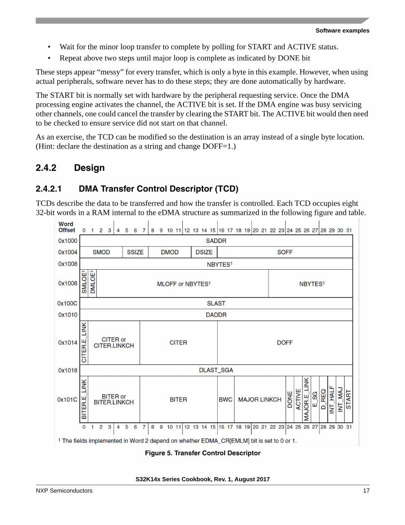
2.4.2.1 DMA Transfer Control Descriptor (TCD)
TCDs describe the data to be transferred and how the transfer is controlled. Each TCD occupies eight 32-bit words in a RAM internal to the eDMA structure as summarized in the following figure and table.
Figure 5. Transfer Control Descriptor
S32K14x Series Cookbook, Rev. 1, August 2017
NXP Semiconductors 17

Software examples
Table 5. TCD initialization with NXP S32K144 header file
TCD Field Option Initialization for TCDn with field value x
SADDR — DMA->TCD[n].SADDR = DMA_TCD_SADDR_SADDR(x)
SOFF — DMA->TCD[n].SOFF = DMA_TCD_SOFF_SOFF(x)
SMODSSIZEDMODDSIZE
—DMA->TCD[n].ATTR.SMODDMA->TCD[n].ATTR.SSIZEDMA->TCD[n].ATTR.DMODDMA->TCD[n].ATTR.DSIZE
====
DMA_TCD_ATTR_SMOD(x)DMA_TCD_ATTR_SSIZE(x)DMA_TCD_ATTR_DMOD(x)DMA_TCD_ATTR_DSIZE(x)
SMLOEDMLOEMLOFFNBYTES
Minor Loop mapping disabled
DMA->TCD[n].NBYTES.MLNO = DMA_TCD_NBYTES_MLNO_NBYTES(x)
Minor Loop mapping enabled and Offset disabled
DMA->TCD[n].NBYTES.MLOFFNODMA->TCD[n].NBYTES.MLOFFNODMA->TCD[n].NBYTES.MLOFFNO
===
DMA_TCD_NBYTES_MLOFFNO_SMLOE(x)DMA_TCD_NBYTES_MLOFFNO_DMLOE(x)DMA_TCD_NBYTES_MLOFFNO_NBYTES(x)
Minor Loop mapping enabled and Offset enabled
DMA->TCD[n].NBYTES.MLOFFYESDMA->TCD[n].NBYTES.MLOFFYESDMA->TCD[n].NBYTES.MLOFFYESDMA->TCD[n].NBYTES.MLOFFYES
====
DMA_TCD_NBYTES_MLOFFYES_SMLOE(x)DMA_TCD_NBYTES_MLOFFYES_DMLOE(x)DMA_TCD_NBYTES_MLOFFYES_MLOFF(x)DMA_TCD_NBYTES_MLOFFYES_NBYTES(x)
SLAST — DMA->TCD[n].SLAST = DMA_TCD_SLAST_SLAST(x)
DADDR — DMA->TCD[n].DADDR = DMA_TCD_DADDR_DADDR(x)
DOFF — DMA->TCD[n].DOFF = DMA_TCD_DOFF_DOFF(x)
CITERCITER.LINKCHCITER.E.LINK
Channel Linking disabled
DMA->TCD[n].CITER.ELINKNODMA->TCD[n].CITER.ELINKNO
==
DMA_TCD_CITER_ELINKNO_CITER(x)DMA_TCD_CITER_ELINKNO_ELINK(x)
Channel Linking enabled
DMA->TCD[n].CITER.ELINKYESDMA->TCD[n].CITER.ELINKYESDMA->TCD[n].CITER.ELINKYES
===
DMA_TCD_CITER_ELINKYES_CITER(x)DMA_TCD_CITER_ELINKYES_LINKCH(x)DMA_TCD_CITER_ELINKYES_ELINK(x)
DLAST_SGA — DMA->TCD[n].DLASTSGA = DMA_TCD_DLASTSGA_DLASTSGA(x)
STARTINT_MAJINT_HALFD_REQE_SGMAJOR.E.LINKACTIVEDONEMAJOR.LINKCHBWC
—
DMA->TCD[n].CSRDMA->TCD[n].CSRDMA->TCD[n].CSRDMA->TCD[n].CSRDMA->TCD[n].CSRDMA->TCD[n].CSRDMA->TCD[n].CSRDMA->TCD[n].CSRDMA->TCD[n].CSRDMA->TCD[n].CSR
==========
DMA_TCD_CSR_START(x)DMA_TCD_CSR_INTMAJOR(x)DMA_TCD_CSR_INTHALF(x)DMA_TCD_CSR_DREQ(x)DMA_TCD_CSR_ESG(x)DMA_TCD_CSR_MAJORELINK(x)DMA_TCD_CSR_ACTIVE(x)DMA_TCD_CSR_DONE(x)DMA_TCD_CSR_MAJORLINKCH(x)DMA_TCD_CSR_BWC(x)
BITERBITER.LINKCHBITER.E_LINK
Channel Linking disabled
DMA->TCD[n].BITER.ELINKNODMA->TCD[n].BITER.ELINKNO
==
DMA_TCD_BITER_ELINKNO_BITER(x)DMA_TCD_BITER_ELINKNO_ELINK(x)
Channel Linking enabled
DMA->TCD[n].BITER.ELINKYESDMA->TCD[n].BITER.ELINKYESDMA->TCD[n].BITER.ELINKYES
===
DMA_TCD_BITER_ELINKYES_BITER(x)DMA_TCD_BITER_ELINKYES_LINKCH(x)DMA_TCD_BITER_ELINKYES_ELINK(x)
S32K14x Series Cookbook, Rev. 1, August 2017
NXP Semiconductors18
Software examples
2.4.2.2 Design Steps
• Disable watchdog
• System clocks: Initialize SOSC for 8 MHz, sysclk 80 MHz, RUN mode for 80 MHz
• Initialize DMA controller:
— Enable clock to DMA MUX module (Not required if software initiates DMA with START bit.)
— Enable desired channels. (Not required if software initiates DMA with START bit.)
• Initialize DMA Transfer Control Descriptors (Only TCD0 is used here):
— Source
– Source address (SADDR): Use address of a string “Hello World”
– Source offset (SOFF): Increment source address by 1 byte for each transfer
– Source modulo (SMOD): Feature not used here
– Source size (SSIZE): Read 1 byte at a time
– Source last address adjustment (SLAST): Decrement source address by 11 after major loop
— Destination
– Destination address (DADDR): Use address of a single byte
– Destination offset (DOFF): Do not add offset to destination address after minor loop
– Destination modulo (DMOD): Feature not used here
– Destination size (DSIZE): Write 1 byte at a time
– Destination last address adjustment (DLAST): Do not adjust address after major loop
— Number of bytes per DMA request and number of iterations (minor loops)
– Number of bytes to be transferred per DMA request (NBYTES): One byte
– Number of iterations/minor loops in major loop (CITER and BITER): 11
– Channel to channel linking for additional iterations after minor loop (BITER ELINK and CITER ELINK): Disabled
— Controls and Status
– Disable channel after major loop completes (DREQ): Disable channel
– Generate interrupt request half way through major loop (INTHALF): Disabled
– Generate interrupt request after completing major loop (INTMAJOR): Disabled
– Enable Scatter-Gather (ESG): Disabled. No other TCDs loaded to channel
– Enable channel link after major loop (MAJORLINK): Disabled
– Channel link number after major loop (MAJORLINKCH): Null - feature disabled
– Band Width Control (BWC): Set to 0 so there are no stalls after R/W
– Clear initial values of status flags (START, ACTIVE, DONE): Set to zero
• Start first transfer (set START = 1) and wait for transfer to complete (START=0, ACTIVE=0)
• Loop: While the channel’s DONE status is not set:
— Start next transfer (set START = 1) and wait for transfer to complete (START=0, ACTIVE=0)
• Clear channel’s DONE status bit
S32K14x Series Cookbook, Rev. 1, August 2017
NXP Semiconductors 19
Software examples
2.4.3 Code
2.4.3.1 main.c
#include "S32K144.h" /* Include peripheral declarations S32K144 */#include "dma.h"#include "clocks_and_modes.h"
void WDOG_disable (void){ WDOG->CNT=0xD928C520; /* Unlock watchdog */ WDOG->TOVAL=0x0000FFFF; /* Maximum timeout value */ WDOG->CS = 0x00002100; /* Disable watchdog */}
int main(void) {
WDOG_disable(); SOSC_init_8MHz(); /* Initialize system oscillator for 8 MHz xtal */ SPLL_init_160MHz(); /* Initialize SPLL to 160 MHz with 8 MHz SOSC */ NormalRUNmode_80MHz(); /* Init clocks: 80 MHz SPLL & core, 40 MHz bus, 20 MHz flash */
DMA_init(); /* Init DMA controller */ DMA_TCD_init(); /* Init DMA Transfer Control Descriptor(s) */
DMA->SSRT = 0; /* Set chan 0 START bit to initiate first minor loop */ while (((DMA->TCD[0].CSR >> DMA_TCD_CSR_START_SHIFT) & 1) | /* Wait for START = 0 */ ((DMA->TCD[0].CSR >> DMA_TCD_CSR_ACTIVE_SHIFT) & 1)) {} /* and ACTIVE = 0 */ /* Now minor loop has completed */
while (!((DMA->TCD[0].CSR >> DMA_TCD_CSR_DONE_SHIFT) & 1) ) { /* Loop till DONE = 1 */ /* Place breakpoint at next instruction & observe expressions TCD0_Source, TCD0_Dest */ DMA->SSRT = 0; /* Set chan 0 START bit to initiate next minor loop */ while (((DMA->TCD[0].CSR >> DMA_TCD_CSR_START_SHIFT) & 1) | /* Wait for START = 0 */ ((DMA->TCD[0].CSR >> DMA_TCD_CSR_ACTIVE_SHIFT) & 1)) {} /* and ACTIVE = 0 */ /* Now minor loop has completed */ }
DMA->TCD[0].CSR &= ~(DMA_TCD_CSR_DONE_MASK); /* Clear DONE bit */
while (1) {} /* Wait forever */}
S32K14x Series Cookbook, Rev. 1, August 2017
NXP Semiconductors20

Software examples
2.4.3.2 DMA.c
#include "S32K144.h" /* include peripheral declarations S32K144 */#include "dma.h"uint8_t TCD0_Source[] = {"Hello World"}; /* TCD 0 source (11 byte string) */uint8_t volatile TCD0_Dest = 0; /* TCD 0 destination (1 byte) */void DMA_init(void) { /* This is an initialization place holder for: */ /* 1. Enabling DMA MUX clock PCC_PCCn[PCC_DMAMUX_INDEX] (not needed when START bit used) */ /* 2. Enabling desired channels by setting ERQ bit (not needed when START bit used) */}void DMA_TCD_init(void) {
/* TCD0: Transfers string to a single memory location */ DMA->TCD[0].SADDR = DMA_TCD_SADDR_SADDR((uint32_t volatile) &TCD0_Source); /* Src */ DMA->TCD[0].SOFF = DMA_TCD_SOFF_SOFF(1); /* Src addr add 1 byte after transfer*/ DMA->TCD[0].ATTR = DMA_TCD_ATTR_SMOD(0) | /* Src modulo feature not used */ DMA_TCD_ATTR_SSIZE(0) | /* Src read 2**0 =1 byte per transfer*/ DMA_TCD_ATTR_DMOD(0) | /* Dest modulo feature not used */ DMA_TCD_ATTR_DSIZE(0); /* Dest write 2**0 =1 byte per trans.*/ DMA->TCD[0].NBYTES.MLNO = DMA_TCD_NBYTES_MLNO_NBYTES(1); /* Transfer 1 byte /minor loop*/ DMA->TCD[0].SLAST = DMA_TCD_SLAST_SLAST(-11); /* Src addr change after major loop*/ DMA->TCD[0].DADDR = DMA_TCD_DADDR_DADDR((uint32_t volatile) &TCD0_Dest);/* Dest. */ DMA->TCD[0].DOFF = DMA_TCD_DOFF_DOFF(0); /* No dest adr offset after transfer*/ DMA->TCD[0].CITER.ELINKNO= DMA_TCD_CITER_ELINKNO_CITER(11) | /* 11 minor loop iterations*/ DMA_TCD_CITER_ELINKNO_ELINK(0); /* No minor loop chan link */ DMA->TCD[0].DLASTSGA = DMA_TCD_DLASTSGA_DLASTSGA(0); /* No dest chg after major loop*/ DMA->TCD[0].CSR = DMA_TCD_CSR_START(0) | /* Clear START status flag */ DMA_TCD_CSR_INTMAJOR(0) | /* No IRQ after major loop */ DMA_TCD_CSR_INTHALF(0) | /* No IRQ after 1/2 major loop */ DMA_TCD_CSR_DREQ(1) | /* Disable chan after major loop*/ DMA_TCD_CSR_ESG(0) | /* Disable Scatter Gather */ DMA_TCD_CSR_MAJORELINK(0) | /* No major loop chan link */ DMA_TCD_CSR_ACTIVE(0) | /* Clear ACTIVE status flag */ DMA_TCD_CSR_DONE(0) | /* Clear DONE status flag */ DMA_TCD_CSR_MAJORLINKCH(0) | /* Chan # if major loop ch link */ DMA_TCD_CSR_BWC(0); /* No eDMA stalls after R/W */ DMA->TCD[0].BITER.ELINKNO= DMA_TCD_BITER_ELINKNO_BITER(11) | /* Initial iteration count*/ DMA_TCD_BITER_ELINKNO_ELINK(0); /* No minor loop chan link */}
2.4.3.3 clocks_and_modes.cSee code in clocks_and_modes.c of the Hello World + Clock example.
S32K14x Series Cookbook, Rev. 1, August 2017
NXP Semiconductors 21

Software examples
2.5 Timed I/O (FTM)
2.5.1 Description
Summary: This example uses the Flex Timer Module (FTM) to perform common digital I/O functions of:
• Edge-Aligned Pulse Width Modulation (EPWM): 1 Hz, low 25%, high 75%
• Output Compare (OC): Toggle output every 100 msec (10 MHz toggle produces 5 MHz frequency)
• Input Capture (IC): Capture input’s rising or falling edge times
All channels in the FTM share a common 16-bit counter for the I/O functions.
Figure 6. Timed I/O example block diagram.
To measure the Input Capture time, connect a wire from J2 pin 8 to pin 4 or pin 2.
FTM0
PTD15
S32K144 EVB
S32K144
ClocksXTAL
8 MHz SOSCDIV1_CLK (8 MHz)
Prescale by
PCC_FLEXTMR0clock select
2PR (128)No clock
FTM Counter:counts to 62500
Channel 0: 10 HzOutput Compare
Channel 1: 1 Hz
Channel 6:Input Capture
Pulse Width Mod.
(1 second)
MUX
CLKS =
Module
(SYS_CLK,clock
Fixed freq clkSYS_CLKExt. clock
Ext. clock (8 MHz)
PTD16
PTE8
RedLED
GreenLED
J22
8
4Edge-Aligned
SYS_CLK (80 MHz)
80 MHz)
S32K14x Series Cookbook, Rev. 1, August 2017
NXP Semiconductors22
Software examples
2.5.2 Design
2.5.2.1 Channel Mode Selection
Channel modes are configured by settings in registers for the entire FTM module and individual channel. The following table shows the settings used for channel modes implemented in this example.
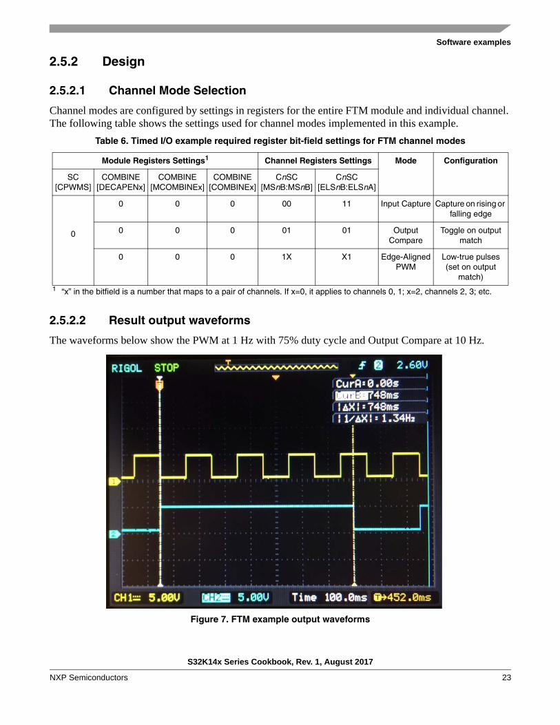
2.5.2.2 Result output waveforms
The waveforms below show the PWM at 1 Hz with 75% duty cycle and Output Compare at 10 Hz.
Figure 7. FTM example output waveforms
Table 6. Timed I/O example required register bit-field settings for FTM channel modes
Module Registers Settings1
1 “x” in the bitfield is a number that maps to a pair of channels. If x=0, it applies to channels 0, 1; x=2, channels 2, 3; etc.
Channel Registers Settings Mode Configuration
SC[CPWMS]
COMBINE[DECAPENx]
COMBINE[MCOMBINEx]
COMBINE[COMBINEx]
CnSC[MSnB:MSnB]
CnSC[ELSnB:ELSnA]
0
0 0 0 00 11 Input Capture Capture on rising or falling edge
0 0 0 01 01 Output Compare
Toggle on output match
0 0 0 1X X1 Edge-Aligned PWM
Low-true pulses (set on output
match)
S32K14x Series Cookbook, Rev. 1, August 2017
NXP Semiconductors 23
Software examples
2.5.2.3 Design Steps
• Disable watchdog
• System clocks: Initialize SOSC for 8 MHz, sysclk for 80 MHz, RUN mode for 80 MHz
• Initialize FTM0. Input clock source will be 8 MHz SOSCDIV1_CLK:
— Disable write protection to FTM0 registers to allow configuration
— Controls:
– Prescale clock source by 128 (8 MHz / 128 = 62500 Hz)
– Enable channels 0, 1 as outputs
– No filtering or interrupts are used
– PWM is configured as up count (CPWMS=0)
– Clock source = none (clock/counter will be started after initializations)
— Initialize mode, polarity settings: CPWMS, DECAPEN, MCOMBINE, COMBINE, polarity=0
— Counter count up value = 62500 (1 second period)
• Initialize FTM0 Channel 0 as Output Compare, toggle on match every 100 msec:
— Configure MSB:MSA, ELSB:ELSA for Output Compare mode
— Set initial compare value to 6250 (for 100 msec)
— Set polarity to active high
• Initialize FTM0 Channel 1 as EPWM, 1 Hz, 75% duty Cycle:
— Configure MSB:MSA, ELSB:ELSA for PWM mode
— Set initial compare value for 75% duty cycle
• Initialize FTM0 Channel 6 as Input Capture, either edge:
— Configure MSB:MSA, ELSB:ELSA for Input Capture mode
• Initialize port pins for FTM0:
— Enable clocks to Port D and Port E modules
— PTD15: FTM0 CH 0 - output compare - connects to red LED
— PTD16: FRM0 CH 1- PWM - connects to green LED
— PTE8: FTM0 CH 6 - input capture
• Start FTM0 counter
• Loop:
— If output compare match flag is set:
– output pin toggles (automatically by hardware)
– update compare value for next 100 msec (6250 added to current count)
— If input capture flag is set, clear flag and read timer:
– clear flag
– store prior capture value
– read current capture value
– calculate delta of prior and current capture values
S32K14x Series Cookbook, Rev. 1, August 2017
NXP Semiconductors24
Software examples
2.5.3 Code
2.5.3.1 main.c
#include "S32K144.h" /* include peripheral declarations S32K144 */#include "clocks_and_modes.h"#include "FTM.h"
void PORT_init (void) { PCC->PCCn[PCC_PORTD_INDEX ]|=PCC_PCCn_CGC_MASK; /* Enable clock for PORTD */ PCC->PCCn[PCC_PORTE_INDEX ]|=PCC_PCCn_CGC_MASK; /* Enable clock for PORTE */ PORTE->PCR[8]|=PORT_PCR_MUX(2); /* Port E8: MUX = ALT2, FTM0CH6 */ PORTD->PCR[15]|=PORT_PCR_MUX(2); /* Port D15: MUX = ALT2, FTM0CH0 */ PORTD->PCR[16]|=PORT_PCR_MUX(2); /* Port D16: MUX = ALT2, FTM0CH1 */}
void WDOG_disable (void) { WDOG->CNT=0xD928C520; /* Unlock watchdog */ WDOG->TOVAL=0x0000FFFF; /* Maximum timeout value */ WDOG->CS = 0x00002100; /* Disable watchdog */}
int main(void) { WDOG_disable(); /* Disable WDOG*/ SOSC_init_8MHz(); /* Initialize system oscillator for 8 MHz xtal */ SPLL_init_160MHz(); /* Initialize SPLL to 160 MHz with 8 MHz SOSC */ NormalRUNmode_80MHz(); /* Init clocks: 80 MHz SPLL & core, 40 MHz bus, 20 MHz flash */ FTM0_init(); /* Init FTM0 */ FTM0_CH0_OC_init(); /* Init FTM0 CH0, red LED */ FTM0_CH1_PWM_init(); /* Init FTM0 CH1, green LED */ FTM0_CH6_IC_init(); /* Init FTM0 CH6, j2-8 */ PORT_init(); /* Configure ports */ start_FTM0_counter(); /* Start FTM0 counter */ for(;;) { FTM0_CH0_output_compare();/* If output compare match: */ /* Pin toggles (automatically by hardware) */ /* Clear flag 8 */ /* Reload timer */ FTM0_CH6_input_capture(); /* If input captured: clear flag, read timer */}
S32K14x Series Cookbook, Rev. 1, August 2017
NXP Semiconductors 25

Software examples
2.5.3.2 FTM.c
#include "S32K144.h" /* include peripheral declarations S32K144 */#include "FTM.h"uint16_t CurrentCaptureVal = 0;uint16_t PriorCaptureVal = 0;uint16_t DeltaCapture = 0;
void FTM0_init(void) { PCC->PCCn[PCC_FLEXTMR0_INDEX] &= ~PCC_PCCn_CGC_MASK; /* Ensure clk disabled for config */ PCC->PCCn[PCC_FLEXTMR0_INDEX] |= PCC_PCCn_PCS(0b001)/* Clock Src=1, 8 MHz SOSCDIV1_CLK */ | PCC_PCCn_CGC_MASK; /* Enable clock for FTM regs */ FTM0->MODE |= FTM_MODE_WPDIS_MASK; /* Write protect to registers disabled (default) */ FTM0->SC = 0x00030007; /* Enable PWM channel 0 output*/ /* Enable PWM channel 1 output*/ /* TOIE (Timer Overflow Interrupt Ena) = 0 (default) */ /* CPWMS (Center aligned PWM Select) = 0 (default, up count) */ /* CLKS (Clock source) = 0 (default, no clock; FTM disabled) */ /* PS (Prescaler factor) = 7. Prescaler = 128 */ FTM0->COMBINE = 0x00000000;/* FTM mode settings used: DECAPENx, MCOMBINEx, COMBINEx=0 */ FTM0->POL = 0x00000000; /* Polarity for all channels is active high (default) */ FTM0->MOD = 62500 -1 ; /* FTM1 counter final value (used for PWM mode) */ /* FTM1 Period = MOD-CNTIN+0x0001 ~= 62500 ctr clks */ /* 8MHz /128 = 62.5kHz -> ticks -> 1Hz */}
void FTM0_CH0_OC_init(void) { FTM0->CONTROLS[0].CnSC = 0x00000014; /* FTM0 ch0: Output Compare, toggle output on match */ /* CHIE (Chan Interrupt Ena)= 0 (default) */ /* MSB:MSA (chan Mode Select)= 0b01, Output Compare */ /* ELSB:ELSA (chan Edge or Level Select)= 0b01, toggle*/ FTM0->CONTROLS[0].CnV= 6250; /* FTM0 ch 0 Compare Value= 6250 clks, 100ms toggle*/ FTM0->POL &= ~FTM_POL_POL0_MASK; /* FTM0 ch 0 polarity = 0 (Default, active high) */}
void FTM0_CH1_PWM_init(void) { FTM0->CONTROLS[1].CnSC = 0x00000028; /* FTM0 ch1: edge-aligned PWM, low true pulses */ /* CHIE (Chan Interrupt Ena) = 0 (default) */ /* MSB:MSA (chan Mode Select)=0b10, Edge Align PWM*/ /* ELSB:ELSA (chan Edge/Level Select)=0b10, low true */ FTM0->CONTROLS[1].CnV = 46875; /* FTM0 ch1 compare value (~75% duty cycle) */}
S32K14x Series Cookbook, Rev. 1, August 2017
NXP Semiconductors26
Software examples
void FTM0_CH6_IC_init(void) { FTM0->CONTROLS[6].CnSC = 0x0000000C; /* FTM0 ch6: Input Capture rising or falling edge */ /* CHIE (Chan Interrupt Ena) = 0 (default) */ /* MSB:MSA (chan Mode Select)=0b00, Input Capture */ /* ELSB:ELSA (ch Edge/Level Select)=0b11, rise or fall*/}
void FTM0_CH0_output_compare(void) { if (1==((FTM0->CONTROLS[0].CnSC & FTM_CnSC_CHF_MASK)>>FTM_CnSC_CHF_SHIFT)) {
/* If chan flag is set */ FTM0->CONTROLS[0].CnSC &= ~FTM_CnSC_CHF_MASK; /* Clear flag: read reg then set CHF=0 */ if( FTM0->CONTROLS[0].CnV==56250) { /* If count at last value before end, */ FTM0->CONTROLS[0].CnV= 0 ; /* Update compare value: to 0*/ } else { FTM0->CONTROLS[0].CnV= FTM0->CONTROLS[0].CnV + 6250 ; /* Update compare value: add 6250 to current value*/ } }}
void FTM0_CH6_input_capture(void) { if (1==((FTM0->CONTROLS[6].CnSC & FTM_CnSC_CHF_MASK)>>FTM_CnSC_CHF_SHIFT)) {
/* If chan flag is set */ FTM0->CONTROLS[6].CnSC &= ~FTM_CnSC_CHF_MASK; /* Clear flag: read reg then set CHF=0 */ PriorCaptureVal = CurrentCaptureVal; /* Record value of prior capture */ CurrentCaptureVal = FTM0->CONTROLS[6].CnV; /* Record value of current capture */ DeltaCapture = CurrentCaptureVal - PriorCaptureVal; /* Will be 6250 clocks (100 msec) if connected to FTM0 CH0 */ }}
void start_FTM0_counter (void) { FTM0->SC |= FTM_SC_CLKS(3); /* Start FTM0 counter with clk source = external clock (SOSCDIV1_CLK)*/}
2.5.3.3 clocks_and_modes.cSee code in clocks_and_modes.c of the Hello World + Clock example.
S32K14x Series Cookbook, Rev. 1, August 2017
NXP Semiconductors 27
Software examples
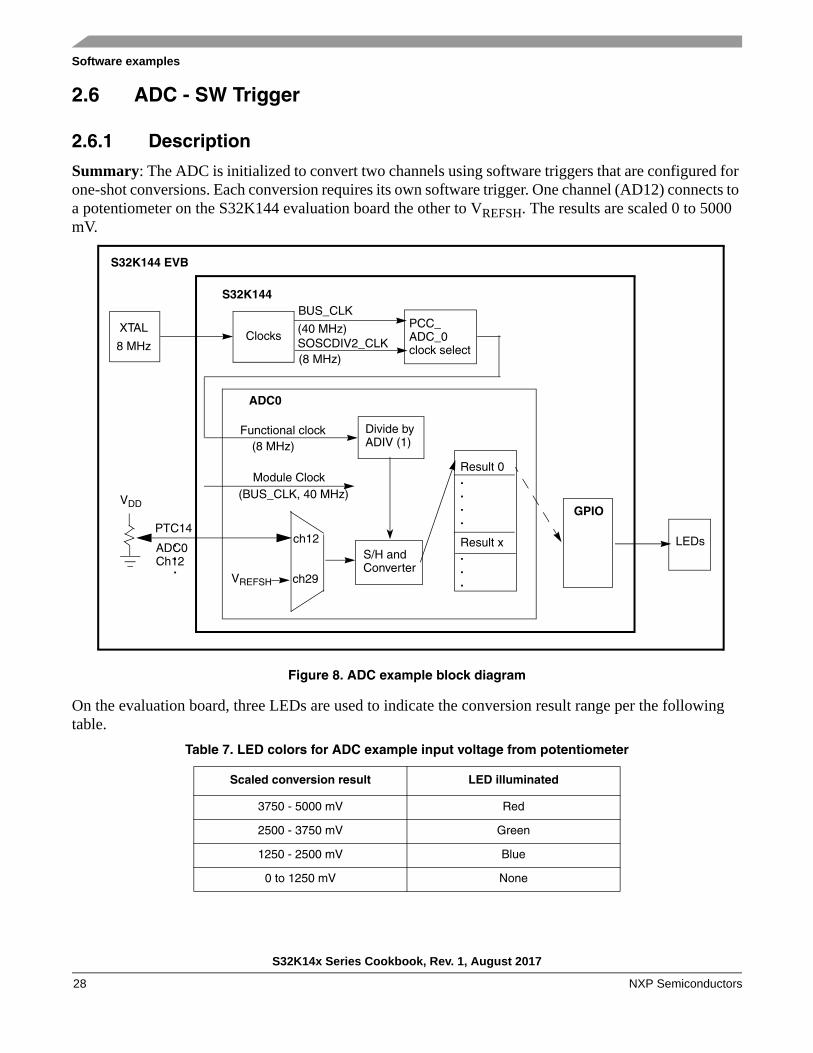
2.6 ADC - SW Trigger
2.6.1 Description
Summary: The ADC is initialized to convert two channels using software triggers that are configured for one-shot conversions. Each conversion requires its own software trigger. One channel (AD12) connects to a potentiometer on the S32K144 evaluation board the other to VREFSH. The results are scaled 0 to 5000 mV.
Figure 8. ADC example block diagram
On the evaluation board, three LEDs are used to indicate the conversion result range per the following table.
Table 7. LED colors for ADC example input voltage from potentiometer
Scaled conversion result LED illuminated
3750 - 5000 mV Red
2500 - 3750 mV Green
1250 - 2500 mV Blue
0 to 1250 mV None
ADC0
S32K144 EVB
S32K144
ClocksXTAL
8 MHz
Divide byFunctional clock (8 MHz)
PCC_ADC_0clock select
Module Clock(BUS_CLK, 40 MHz)
(8 MHz)
BUS_CLK
(40 MHz)SOSCDIV2_CLK
LEDs
ADIV (1)
VDD
S/H andConverter
.
.
.
ch12
Result 0...
Result x...
GPIO.
ch29VREFSH
PTC14
ADC0 Ch12
S32K14x Series Cookbook, Rev. 1, August 2017
NXP Semiconductors28

Software examples
2.6.2 Design
ADC calibration is not included in this simple example. Hence the results can be lower than the specified accuracy. The steps to initialize the calibration mechanism are found in the Calibration function section of the ADC chapter of the reference manual.
• Disable watchdog
• System clocks: Initialize SOSC for 8 MHz, sysclk for 80 MHz, RUN mode for 80 MHz
• Initialize port pins:
— Enable clocks to Port D
— PTD0: GPIO output - connects to blue LED
— PTD15: GPIO output - connects to red LED
— PTD16: GPIO output- connects to green LED
— (Out of reset, no configuration is needed for analog pins.)
• Initialize ADC:
— Select SOSCDIV2_CLK for functional clock and enable it to module
— Disable module and disable interrupt requests from module (reset default state)
— Configure ADC for 12-bit conversions using SOSCDIV2_CLK, divided by 1
— Configure sample time of 13 ADCK clock cycles (reset default value)
— Select software trigger for conversions, no compare functions, no DMA and use default voltage reference pins - external pins VREFH and VREFL. (reset default value)
— Disable continuous conversions (so there is one conversion per software trigger), disable hardware averaging, disable calibration sequence start up
• Loop:
— Issue ADC conversion command for channel 12, which is connected to the potentiometer on the NXP evaluation board. (Use ADC_SC1[0] for software triggers.)
— Wait for conversion complete flag. When conversion is complete:
– Read result and scale to 0 to 5000 mV (Result is in ADC_R[0] for all software triggers.)
– Illuminate LED per voltage range
— Issue ADC conversion command to read channel 29, ADC high reference voltage (Use ADC_SC1[0] for software triggers.)
— Wait for conversion complete flag. When conversion is complete:
– Read result and scale to 0 to 5000 mV (Result is in ADC_R[0] for all software triggers.)
S32K14x Series Cookbook, Rev. 1, August 2017
NXP Semiconductors 29
Software examples
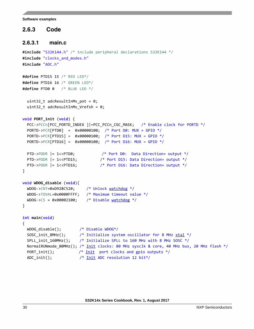
2.6.3 Code
2.6.3.1 main.c
#include "S32K144.h" /* include peripheral declarations S32K144 */#include "clocks_and_modes.h"#include "ADC.h"
#define PTD15 15 /* RED LED*/#define PTD16 16 /* GREEN LED*/#define PTD0 0 /* BLUE LED */
uint32_t adcResultInMv_pot = 0; uint32_t adcResultInMv_Vrefsh = 0;
void PORT_init (void) { PCC->PCCn[PCC_PORTD_INDEX ]|=PCC_PCCn_CGC_MASK; /* Enable clock for PORTD */ PORTD->PCR[PTD0] = 0x00000100; /* Port D0: MUX = GPIO */ PORTD->PCR[PTD15] = 0x00000100; /* Port D15: MUX = GPIO */ PORTD->PCR[PTD16] = 0x00000100; /* Port D16: MUX = GPIO */
PTD->PDDR |= 1<<PTD0; /* Port D0: Data Direction= output */ PTD->PDDR |= 1<<PTD15; /* Port D15: Data Direction= output */ PTD->PDDR |= 1<<PTD16; /* Port D16: Data Direction= output */}
void WDOG_disable (void){ WDOG->CNT=0xD928C520; /* Unlock watchdog */ WDOG->TOVAL=0x0000FFFF; /* Maximum timeout value */ WDOG->CS = 0x00002100; /* Disable watchdog */}
int main(void){ WDOG_disable(); /* Disable WDOG*/ SOSC_init_8MHz(); /* Initialize system oscillator for 8 MHz xtal */ SPLL_init_160MHz(); /* Initialize SPLL to 160 MHz with 8 MHz SOSC */ NormalRUNmode_80MHz(); /* Init clocks: 80 MHz sysclk & core, 40 MHz bus, 20 MHz flash */ PORT_init(); /* Init port clocks and gpio outputs */ ADC_init(); /* Init ADC resolution 12 bit*/
S32K14x Series Cookbook, Rev. 1, August 2017
NXP Semiconductors30
Software examples
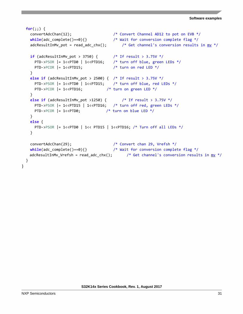
for(;;) { convertAdcChan(12); /* Convert Channel AD12 to pot on EVB */ while(adc_complete()==0){} /* Wait for conversion complete flag */ adcResultInMv_pot = read_adc_chx(); /* Get channel's conversion results in mv */
if (adcResultInMv_pot > 3750) { /* If result > 3.75V */ PTD->PSOR |= 1<<PTD0 | 1<<PTD16; /* turn off blue, green LEDs */ PTD->PCOR |= 1<<PTD15; /* turn on red LED */ } else if (adcResultInMv_pot > 2500) { /* If result > 3.75V */ PTD->PSOR |= 1<<PTD0 | 1<<PTD15; /* turn off blue, red LEDs */ PTD->PCOR |= 1<<PTD16; /* turn on green LED */ } else if (adcResultInMv_pot >1250) { /* If result > 3.75V */ PTD->PSOR |= 1<<PTD15 | 1<<PTD16; /* turn off red, green LEDs */ PTD->PCOR |= 1<<PTD0; /* turn on blue LED */ } else { PTD->PSOR |= 1<<PTD0 | 1<< PTD15 | 1<<PTD16; /* Turn off all LEDs */ }
convertAdcChan(29); /* Convert chan 29, Vrefsh */ while(adc_complete()==0){} /* Wait for conversion complete flag */ adcResultInMv_Vrefsh = read_adc_chx(); /* Get channel's conversion results in mv */ }}
S32K14x Series Cookbook, Rev. 1, August 2017
NXP Semiconductors 31
Software examples
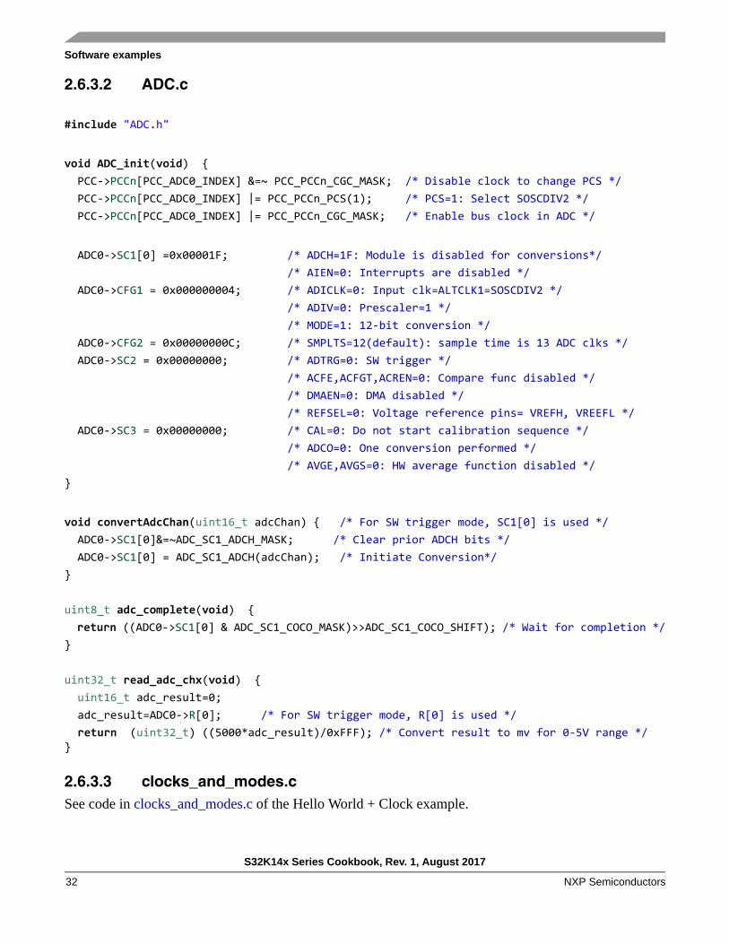
2.6.3.2 ADC.c
#include "ADC.h"
void ADC_init(void) { PCC->PCCn[PCC_ADC0_INDEX] &=~ PCC_PCCn_CGC_MASK; /* Disable clock to change PCS */ PCC->PCCn[PCC_ADC0_INDEX] |= PCC_PCCn_PCS(1); /* PCS=1: Select SOSCDIV2 */ PCC->PCCn[PCC_ADC0_INDEX] |= PCC_PCCn_CGC_MASK; /* Enable bus clock in ADC */
ADC0->SC1[0] =0x00001F; /* ADCH=1F: Module is disabled for conversions*/ /* AIEN=0: Interrupts are disabled */ ADC0->CFG1 = 0x000000004; /* ADICLK=0: Input clk=ALTCLK1=SOSCDIV2 */ /* ADIV=0: Prescaler=1 */ /* MODE=1: 12-bit conversion */ ADC0->CFG2 = 0x00000000C; /* SMPLTS=12(default): sample time is 13 ADC clks */ ADC0->SC2 = 0x00000000; /* ADTRG=0: SW trigger */ /* ACFE,ACFGT,ACREN=0: Compare func disabled */ /* DMAEN=0: DMA disabled */ /* REFSEL=0: Voltage reference pins= VREFH, VREEFL */ ADC0->SC3 = 0x00000000; /* CAL=0: Do not start calibration sequence */ /* ADCO=0: One conversion performed */ /* AVGE,AVGS=0: HW average function disabled */}
void convertAdcChan(uint16_t adcChan) { /* For SW trigger mode, SC1[0] is used */ ADC0->SC1[0]&=~ADC_SC1_ADCH_MASK; /* Clear prior ADCH bits */ ADC0->SC1[0] = ADC_SC1_ADCH(adcChan); /* Initiate Conversion*/}
uint8_t adc_complete(void) { return ((ADC0->SC1[0] & ADC_SC1_COCO_MASK)>>ADC_SC1_COCO_SHIFT); /* Wait for completion */}
uint32_t read_adc_chx(void) { uint16_t adc_result=0; adc_result=ADC0->R[0]; /* For SW trigger mode, R[0] is used */ return (uint32_t) ((5000*adc_result)/0xFFF); /* Convert result to mv for 0-5V range */}
2.6.3.3 clocks_and_modes.cSee code in clocks_and_modes.c of the Hello World + Clock example.
S32K14x Series Cookbook, Rev. 1, August 2017
NXP Semiconductors32

Software examples
2.7 UART
2.7.1 Description
Summary: This example performs a simple UART 9600 baud transfer to a COM port on a PC. FIFOs, interrupts and DMA are not implemented.
The Open SDA interface can be used on the evaluation board, where the UART signals are transferred to a USB interface, which can connect to a PC which has a terminal emulation program such as PUTTY, TeraTerm or other software.
Figure 9. UART example block diagram
LPUART1
TxFIFO
Shift Register
RxFIFO
PTC6 UART1_RX
S32K144 EVB
S32K144
Level shifters and
ClocksXTAL
8 MHz SOSCDIV2_CLK (8 MHz)
PTC7 UART1_TX
DATA
DATA
Divide byFunctional clock (8 MHz)
PCC_LPUART_1clock select
Open SDA Interface
PC with terminalemulator software
USB
16xSBR(16x5=832)
Baud rate clock(9600 Hz)
Moduleclock(BUS_CLK,
BUS_CLK (40 MHz)
40 MHz)
S32K14x Series Cookbook, Rev. 1, August 2017
NXP Semiconductors 33
Software examples
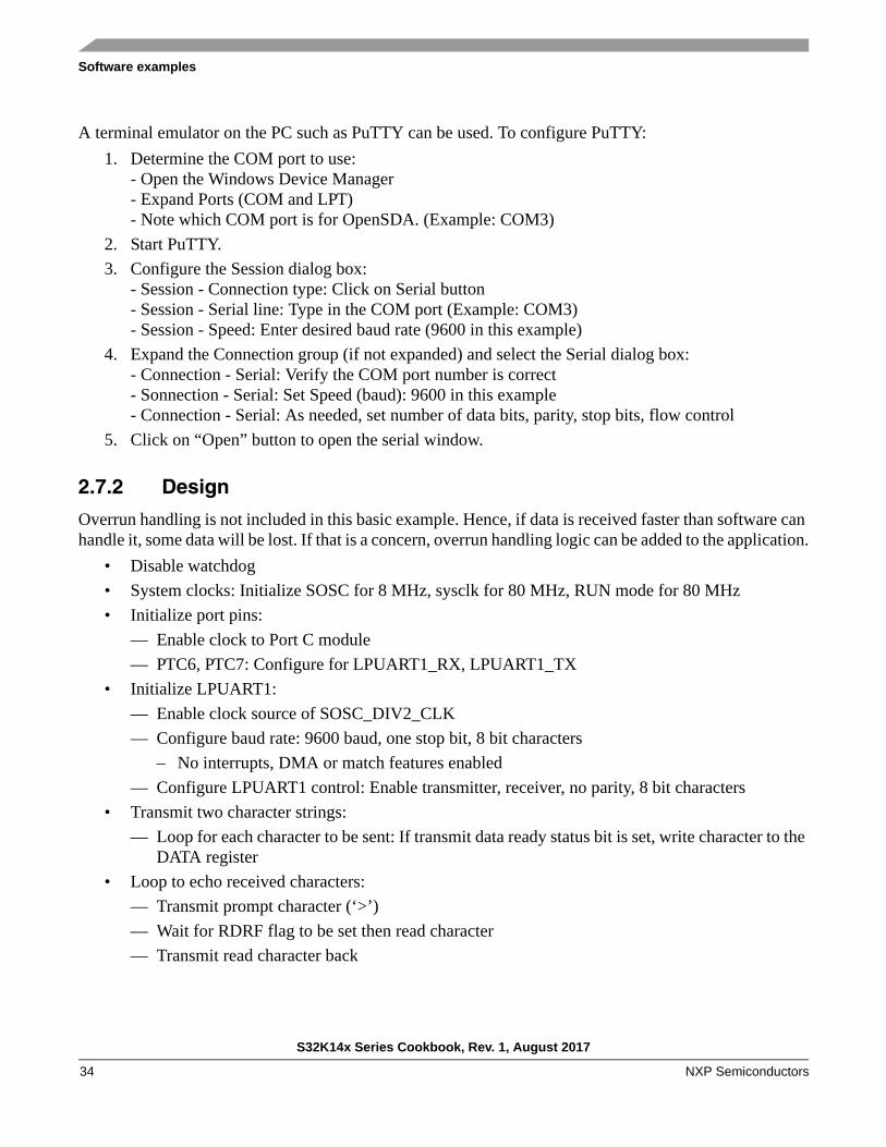
A terminal emulator on the PC such as PuTTY can be used. To configure PuTTY:
1. Determine the COM port to use: - Open the Windows Device Manager - Expand Ports (COM and LPT) - Note which COM port is for OpenSDA. (Example: COM3)
2. Start PuTTY.
3. Configure the Session dialog box:- Session - Connection type: Click on Serial button- Session - Serial line: Type in the COM port (Example: COM3)- Session - Speed: Enter desired baud rate (9600 in this example)
4. Expand the Connection group (if not expanded) and select the Serial dialog box:- Connection - Serial: Verify the COM port number is correct- Sonnection - Serial: Set Speed (baud): 9600 in this example- Connection - Serial: As needed, set number of data bits, parity, stop bits, flow control
5. Click on “Open” button to open the serial window.
2.7.2 Design
Overrun handling is not included in this basic example. Hence, if data is received faster than software can handle it, some data will be lost. If that is a concern, overrun handling logic can be added to the application.
• Disable watchdog
• System clocks: Initialize SOSC for 8 MHz, sysclk for 80 MHz, RUN mode for 80 MHz
• Initialize port pins:
— Enable clock to Port C module
— PTC6, PTC7: Configure for LPUART1_RX, LPUART1_TX
• Initialize LPUART1:
— Enable clock source of SOSC_DIV2_CLK
— Configure baud rate: 9600 baud, one stop bit, 8 bit characters
– No interrupts, DMA or match features enabled
— Configure LPUART1 control: Enable transmitter, receiver, no parity, 8 bit characters
• Transmit two character strings:
— Loop for each character to be sent: If transmit data ready status bit is set, write character to the DATA register
• Loop to echo received characters:
— Transmit prompt character (‘>’)
— Wait for RDRF flag to be set then read character
— Transmit read character back
S32K14x Series Cookbook, Rev. 1, August 2017
NXP Semiconductors34
Software examples
2.7.3 Code
2.7.3.1 main.c
#include "S32K144.h" /* include peripheral declarations S32K144 */#include "clocks_and_modes.h"#include "LPUART.h"
char data=0;void PORT_init (void) { PCC->PCCn[PCC_PORTC_INDEX ]|=PCC_PCCn_CGC_MASK; /* Enable clock for PORTC */ PORTC->PCR[6]|=PORT_PCR_MUX(2); /* Port C6: MUX = ALT2,UART1 TX */ PORTC->PCR[7]|=PORT_PCR_MUX(2); /* Port C7: MUX = ALT2,UART1 RX */}
void WDOG_disable (void){ WDOG->CNT=0xD928C520; /* Unlock watchdog */ WDOG->TOVAL=0x0000FFFF; /* Maximum timeout value */ WDOG->CS = 0x00002100; /* Disable watchdog */}
int main(void){ WDOG_disable(); /* Disable WDGO*/ SOSC_init_8MHz(); /* Initialize system oscillator for 8 MHz xtal */ SPLL_init_160MHz(); /* Initialize SPLL to 160 MHz with 8 MHz SOSC */ RUNmode_80MHz(); /* Init clocks: 80 MHz SPLL & core, 40 MHz bus, 20 MHz flash */ PORT_init(); /* Configure ports */
LPUART1_init(); /* Initialize LPUART @ 9600*/ LPUART1_transmit_string("Running LPUART example\n\r"); /* Transmit char string */ LPUART1_transmit_string("Input character to echo...\n\r"); /* Transmit char string */
for(;;) { LPUART1_transmit_char('>'); /* Transmit prompt character*/ LPUART1_receive_and_echo_char();/* Wait for input char, receive & echo it*/
}}
S32K14x Series Cookbook, Rev. 1, August 2017
NXP Semiconductors 35
Software examples
2.7.3.2 LPUART.c
#include "S32K144.h" /* include peripheral declarations S32K144 */#include "LPUART.h"
void LPUART1_init(void) /* Init. summary: 9600 baud, 1 stop bit, 8 bit format, no parity */{ PCC->PCCn[PCC_LPUART1_INDEX] &= ~PCC_PCCn_CGC_MASK; /* Ensure clk disabled for config */ PCC->PCCn[PCC_LPUART1_INDEX] |= PCC_PCCn_PCS(0b001) /* Clock Src= 1 (SOSCDIV2_CLK) */ | PCC_PCCn_CGC_MASK; /* Enable clock for LPUART1 regs */
LPUART1->BAUD = 0x0F000034; /* Initialize for 9600 baud, 1 stop: */ /* SBR=52 (0x34): baud divisor = 8M/9600/16 = ~52 */ /* OSR=15: Over sampling ratio = 15+1=16 */ /* SBNS=0: One stop bit */ /* BOTHEDGE=0: receiver samples only on rising edge */ /* M10=0: Rx and Tx use 7 to 9 bit data characters */ /* RESYNCDIS=0: Resync during rec'd data word supported */ /* LBKDIE, RXEDGIE=0: interrupts disable */ /* TDMAE, RDMAE, TDMAE=0: DMA requests disabled */ /* MAEN1, MAEN2, MATCFG=0: Match disabled */
LPUART1->CTRL=0x000C0000; /* Enable transmitter & receiver, no parity, 8 bit char: */ /* RE=1: Receiver enabled */ /* TE=1: Transmitter enabled */ /* PE,PT=0: No hw parity generation or checking */ /* M7,M,R8T9,R9T8=0: 8-bit data characters*/ /* DOZEEN=0: LPUART enabled in Doze mode */ /* ORIE,NEIE,FEIE,PEIE,TIE,TCIE,RIE,ILIE,MA1IE,MA2IE=0: no IRQ*/ /* TxDIR=0: TxD pin is input if in single-wire mode */ /* TXINV=0: TRansmit data not inverted */ /* RWU,WAKE=0: normal operation; rcvr not in statndby */ /* IDLCFG=0: one idle character */ /* ILT=0: Idle char bit count starts after start bit */ /* SBK=0: Normal transmitter operation - no break char */ /* LOOPS,RSRC=0: no loop back */}
S32K14x Series Cookbook, Rev. 1, August 2017
NXP Semiconductors36

Software examples
void LPUART1_transmit_char(char send) { /* Function to Transmit single Char */ while((LPUART1->STAT & LPUART_STAT_TDRE_MASK)>>LPUART_STAT_TDRE_SHIFT==0); /* Wait for transmit buffer to be empty */ LPUART1->DATA=send; /* Send data */}
void LPUART1_transmit_string(char data_string[]) { /* Function to Transmit whole string */ uint32_t i=0; while(data_string[i] != '\0') { /* Send chars one at a time */ LPUART1_transmit_char(data_string[i]); i++; }}
char LPUART1_receive_char(void) { /* Function to Receive single Char */ char receive; while((LPUART1->STAT & LPUART_STAT_RDRF_MASK)>>LPUART_STAT_RDRF_SHIFT==0); /* Wait for received buffer to be full */ receive= LPUART1->DATA; /* Read received data*/ return receive;}
void LPUART1_receive_and_echo_char(void) { /* Function to echo received char back */ char send = LPUART1_receive_char(); /* Receive Char */ LPUART1_transmit_char(send); /* Transmit same char back to the sender */ LPUART1_transmit_char('\n'); /* New line */}
2.7.3.3 clocks_and_modes.c
See code in clocks_and_modes.c of the Hello World + Clock example.
S32K14x Series Cookbook, Rev. 1, August 2017
NXP Semiconductors 37
Software examples
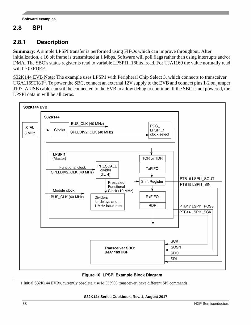
2.8 SPI
2.8.1 Description
Summary: A simple LPSPI transfer is performed using FIFOs which can improve throughput. After initialization, a 16 bit frame is transmitted at 1 Mbps. Software will poll flags rather than using interrupts and/or DMA. The SBC’s status register is read to variable LPSPI1_16bits_read. For UJA1169 the value normally read will be 0xFDEF.
S32K144 EVB Note: The example uses LPSP1 with Peripheral Chip Select 3, which connects to transceiver UGA1169TK/F1. To power the SBC, connect an external 12V supply to the EVB and connect pins 1-2 on jumper J107. A USB cable can still be connected to the EVB to allow debug to continue. If the SBC is not powered, the LPSPI data in will be all zeros.
Figure 10. LPSPI Example Block Diagram
1.Initial S32K144 EVBs, currently obsolete, use MC33903 transceiver, have different SPI commands.
LPSPI1(Master)
TxFIFO
Shift Register
RxFIFO
PTB16 LSPI1_SOUT
S32K144 EVB
S32K144
ClocksXTAL
8 MHz SPLLDIV2_CLK (40 MHz)
PTB15 LSPI1_SIN
TCR or TDR
RDR
PRESCALEdivider
Dividersfor delays and1 MHz baud rate
Functional clock
(div. 4) SPLLDIV2_CLK (40 MHz)
Prescaled
PCC_LPSPI_1clock select
PTB14 LSPI1_SCK
PTB17 LSPI1_PCS3
SCK
SDI
SCSN
SDO
Module clock
BUS_CLK (40 MHz)
Functional Clock (10 MHz)
BUS_CLK (40 MHz)
Transceiver SBC:UJA1169TK/F
S32K14x Series Cookbook, Rev. 1, August 2017
NXP Semiconductors38

Software examples
2.8.2 Design • Disable watchdog
• System clocks: Initialize SOSC for 8 MHz, sysclk for 80 MHz, RUN mode for 80 MHz
• Initialize LPSPI1:
— Module control:
– Disable module to allow configuration
— Configure LPSPI as master
— Initialize clock desired configurations for a 10 MHz prescaled functional clock (100 usec period):
– Prescaled functional clock frequency = Functional clock / PRESCALE = 40 MHz / 4 = 10 MHz
– SCK baud rate = (Functional clock / PRESCALE) / (SCKDIV+2)= (40 MHz / 4) / (8 + 2) = 10 MHz / 10 = 1 MHz
– SCK to PCS delay = 5 prescaled functional clocks = 50 nesc
– PCS to CSK delay = 10 prescaled functional clocks = 1 usec
– Delay between transfers = 10 prescaled functional clocks = 1 usec.
— FIFO Control:
– RxFIFO: Receive Data Flag (RDF) set when # words in FIFO > 0
– TxFIFO: Transmit Data Flag (TDF) set when # words in FIFO < = 3
— Configure Transmit Commands (other configurations could be applied later, for example, for data that uses a different chip select and frame size):
– Prescale functional clock by 8 (80 MHz / 8 = 10 MHz prescaled functional clock)
– Frame size = 16 bits
– PCS3 used for peripheral chip select
– SCK polarity active low
– Phase: Data changed on SCK leading edge, captured on SCK trailing edge
– MSB first, byte swap disabled, continuous transfer disabled
– Single bit width for transfer
– Normal FIFO use: Rx data stored in Rx FIFO, Tx data loaded from Tx FIFO
— Module Control:
– Enable module, including in debug and doze modes
• Initialize port pins for LPSPI1
• Loop:
— Wait for Transmit Data Flag (TDF) to be set (indicates Transmit FIFO availability), then write one SPI frame to Transmit FIFO and clear flag
— Wait for Receive Data Flag (RDF) to set (indicates Receive FIFO has data to read), then read received SPI frame and clear flag. Expected data: 0xFDEF from UJA1169TK/F
— Increase counter
S32K14x Series Cookbook, Rev. 1, August 2017
NXP Semiconductors 39

Software examples
2.8.3 Code
2.8.3.1 main.c
#include "S32K144.h" /* include peripheral declarations S32K144 */#include "LPSPI.h"#include "clocks_and_modes.h"
uint16_t tx_16bits = 0xFD00; /* SBC UJA1169: read Dev ID Reg @ 0x7E (expect non-zero)*/ /* Note: Obsolete EVB with MC33903 example used 0c2580 */ /* to read SAFE reg flags (expect nonzero result).*/ uint16_t LPSPI1_16bits_read; /* Returned data in to SPI */
void WDOG_disable (void){ WDOG->CNT=0xD928C520; /*Unlock watchdog*/ WDOG->TOVAL=0x0000FFFF; /*Maximum timeout value*/ WDOG->CS = 0x00002100; /*Disable watchdog*/}
void PORT_init (void) { PCC->PCCn[PCC_PORTB_INDEX ]|=PCC_PCCn_CGC_MASK; /* Enable clock for PORTB */ PORTB->PCR[14]|=PORT_PCR_MUX(3); /* Port B14: MUX = ALT3, LPSPI1_SCK */ PORTB->PCR[15]|=PORT_PCR_MUX(3); /* Port B15: MUX = ALT3, LPSPI1_SIN */ PORTB->PCR[16]|=PORT_PCR_MUX(3); /* Port B16: MUX = ALT3, LPSPI1_SOUT */ PORTB->PCR[17]|=PORT_PCR_MUX(3); /* Port B17: MUX = ALT3, LPSPI1_PCS3 */}
int main(void) { uint32_t counter = 0; WDOG_disable(); SOSC_init_8MHz(); /* Initialize system oscillator for 8 MHz xtal */ SPLL_init_160MHz(); /* Initialize SPLL to 160 MHz with 8 MHz SOSC */ NormalRUNmode_80MHz(); /* Init clocks: 80 MHz sysclk & core, 40 MHz bus, 20 MHz flash */ LPSPI1_init_master(); /* Initialize LPSPI 1 as master */ PORT_init(); /* Configure ports */ for(;;) { LPSPI1_transmit_16bits(tx_16bits); /* Transmit half word (16 bits) on LPSPI1 */ LPSPI1_16bits_read = LPSPI1_receive_16bits(); /* Receive half word on LSPI1 */ counter++; }
S32K14x Series Cookbook, Rev. 1, August 2017
NXP Semiconductors40

Software examples
2.8.3.2 LPSPI.c
#include "S32K144.h" /* include peripheral declarations S32K144 */#include "LPSPI.h"void LPSPI1_init_master(void) { PCC->PCCn[PCC_LPSPI1_INDEX] = 0; /* Disable clocks to modify PCS ( default) */ PCC->PCCn[PCC_LPSPI1_INDEX] = 0xC6000000; /* Enable PCS=SPLL_DIV2 (40 MHz func'l clock) */ LPSPI1->CR = 0x00000000; /* Disable module for configuration */ LPSPI1->IER = 0x00000000; /* Interrupts not used */ LPSPI1->DER = 0x00000000; /* DMA not used */ LPSPI1->CFGR0 = 0x00000000; /* Defaults: */ /* RDM0=0: rec'd data to FIFO as normal */ /* CIRFIFO=0; Circular FIFO is disabled */ /* HRSEL, HRPOL, HREN=0: Host request disabled */ LPSPI1->CFGR1 = 0x00000001; /* Configurations: master mode*/ /* PCSCFG=0: PCS[3:2] are enabled */ /* OUTCFG=0: Output data retains last value when CS negated */ /* PINCFG=0: SIN is input, SOUT is output */ /* MATCFG=0: Match disabled */ /* PCSPOL=0: PCS is active low */ /* NOSTALL=0: Stall if Tx FIFO empty or Rx FIFO full */ /* AUTOPCS=0: does not apply for master mode */ /* SAMPLE=0: input data sampled on SCK edge */ /* MASTER=1: Master mode */ LPSPI1->TCR = 0x5300000F; /* Transmit cmd: PCS3, 16bits, prescale func'l clk by 4. */ /* CPOL=0: SCK inactive state is low */ /* CPHA=1: Change data on SCK lead'g, capture on trail'g edge*/ /* PRESCALE=2: Functional clock divided by 2**2 = 4 */ /* PCS=3: Transfer using PCS3 */ /* LSBF=0: Data is transferred MSB first */ /* BYSW=0: Byte swap disabled */ /* CONT, CONTC=0: Continuous transfer disabled */ /* RXMSK=0: Normal transfer: rx data stored in rx FIFO */ /* TXMSK=0: Normal transfer: data loaded from tx FIFO */ /* WIDTH=0: Single bit transfer */ /* FRAMESZ=15: # bits in frame = 15+1=16 */ LPSPI1->CCR = 0x04090808; /* Clk dividers based on prescaled func'l clk of 100 nsec */ /* SCKPCS=4: SCK to PCS delay = 4+1 = 5 (500 nsec) */ /* PCSSCK=4: PCS to SCK delay = 9+1 = 10 (1 usec) */ /* DBT=8: Delay between Transfers = 8+2 = 10 (1 usec) */ /* SCKDIV=8: SCK divider =8+2 = 10 (1 usec: 1 MHz baud rate) */ LPSPI1->FCR = 0x00000003; /* RXWATER=0: Rx flags set when Rx FIFO >0 */ /* TXWATER=3: Tx flags set when Tx FIFO <= 3 */
S32K14x Series Cookbook, Rev. 1, August 2017
NXP Semiconductors 41
Software examples
LPSPI1->CR = 0x00000009; /* Enable module for operation */ /* DBGEN=1: module enabled in debug mode */ /* DOZEN=0: module enabled in Doze mode */ /* RST=0: Master logic not reset */ /* MEN=1: Module is enabled */}
void LPSPI1_transmit_16bits (uint16_t send) { while((LPSPI1->SR & LPSPI_SR_TDF_MASK)>>LPSPI_SR_TDF_SHIFT==0); /* Wait for Tx FIFO available */ LPSPI1->TDR = send; /* Transmit data */ LPSPI1->SR |= LPSPI_SR_TDF_MASK; /* Clear TDF flag */}
uint16_t LPSPI1_receive_16bits (void) { uint16_t receive = 0; while((LPSPI1->SR & LPSPI_SR_RDF_MASK)>>LPSPI_SR_RDF_SHIFT==0); /* Wait at least one RxFIFO entry */ receive= LPSPI1->RDR; /* Read received data */ LPSPI1->SR |= LPSPI_SR_RDF_MASK; /* Clear RDF flag */ return receive; /* Return received data */}
2.8.3.3 clocks_and_modes.cSee code in clocks_and_modes.c of the Hello World + Clock example.
S32K14x Series Cookbook, Rev. 1, August 2017
NXP Semiconductors42

Software examples
2.9 CAN 2.0
2.9.1 Description
Summary: A FlexCAN module is initialized for 500 KHz (2 usec period) bit time based on an 8 MHz crystal. Message buffer 0 transmits 8 byte messages and message buffer 4 can receive 8 byte messages.
This example is intended for two EVBs to be connected together, “Node A” and “Node B”. After Node A is initialized it transmits an initial message. Node A then loops: wait to receive a message from Node B then transmit one back. After Node B is intialized it loops waits to receive a message from Node A then transmits one back.
Initial EVBs, now obsolete, used transceiver MC33903. Code and SBC operation fot it is included for reference in the design section.
Figure 11. CAN example block diagram. If using two boards, Node A and B transmit / receive different IDs.
FlexCAN 0
S32K144 EVB
S32K144
ClocksXTAL
8 MHz
SYS_CLK (80 MHz)
SYS_CLK
TXD
RXD
PTE5 CAN0_TX
PTE4 CAN0_RX
CANH
CANL
SOSCDIV2_CLK
(8 MHz)
Divide by 1(PRESDIV+1)MUX
CLK_SRC = 8 MHz SOSCDIV2_CLK
Msg Buffer 0: Node A Tx ID 0x555
8 MHz
J13
1
2
Msg Buffer 4: Node A Rx ID 0x511
Module clock
(SYS_CLK, 80 MHz)
SOSCDIV2_CLK
(8 MHz)
J6-20
J6-18
To CAN Bus
Sclock (Tq)
CANCLK
60 60
Node B Tx ID 0x511
Node B Rx ID 0x555
Transceiver SBC
UJA1169TK/F
GPIOPTD16 (Green LED)Software toggles
output every 1KCAN messages
S32K14x Series Cookbook, Rev. 1, August 2017
NXP Semiconductors 43
Software examples
2.9.2 Design
2.9.2.1 CAN 2.0 timing calculations
These common guidelines are used in CAN 2.0 example for a desired bit rate of 500 KHz:
• CAN bit rate period is typically subdivided into 12–20 time quanta1.
• The sample point is normally chosen around 75%–80% through the bit rate period.
• The remaining 20–25% will be the value for Phase_Seg2.
• The value of Phase_Seg1 will be the same as Phase_Seg2.
• The Sync_Seg is 1 time quantum.
• Resync Jump Width (RJW+1) = Phase_Seg2 (if Phase_Seg2 < 4; otherwise (RJW +1) = 4.
For this example and within the above guidelines, these are the values selected for the CAN module:
• Number of time quanta per bit rate period = 16
• Sample point = 75%, which is 12 time quanta into the 16 time quantum period
Hence,
Phase_Seg2 = (100% – 75%) × 16 time quanta = 25% × 16 time quanta = 4 time quanta; PSEG2 = 3
Phase_Seg1 = Phase_Seg2 = 4 time quanta; PSEG1 = 3
Prop_Seg = 16 – Phase_Seg1 – Phase_Seg2 – SYNCSEG = 16 – 4 – 4 – 1 = 7; PROPSEG = 6
Resync Jump Width (RJW + 1) = 4
Also for this example, the following applies for an 8 MHz crystal.
fCANCLK = 8 MHz (EVB oscillator)
Hence,
fSclock (time quantum freq.) = (16 time quanta/bit rate period) × (500 K bit rate periods/sec)= 8MHz
Prescaler Value (PRESDIV + 1) = fCANCLK / fSclock = 8 MHz / 8 MHz = 1
PRESDIV = 1 – 1 = 0
1.“quantum” is the singular term; “quanta” is the plural term.
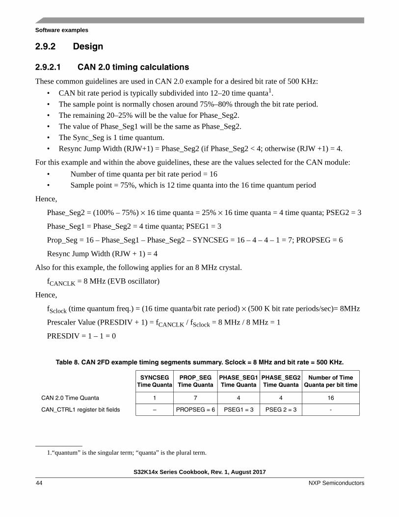
Table 8. CAN 2FD example timing segments summary. Sclock = 8 MHz and bit rate = 500 KHz.
SYNCSEGTime Quanta
PROP_SEG Time Quanta
PHASE_SEG1 Time Quanta
PHASE_SEG2 Time Quanta
Number of Time Quanta per bit time
CAN 2.0 Time Quanta 1 7 4 4 16
CAN_CTRL1 register bit fields – PROPSEG = 6 PSEG1 = 3 PSEG 2 = 3 -
S32K14x Series Cookbook, Rev. 1, August 2017
NXP Semiconductors44
Software examples
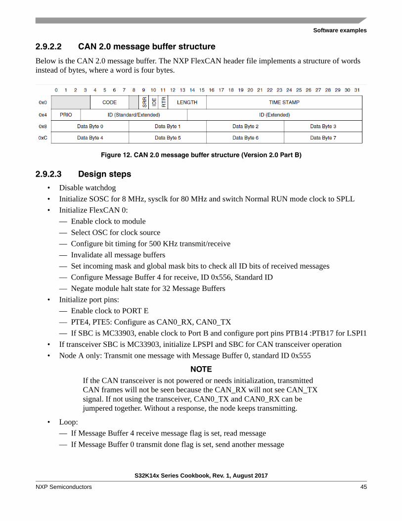
2.9.2.2 CAN 2.0 message buffer structure
Below is the CAN 2.0 message buffer. The NXP FlexCAN header file implements a structure of words instead of bytes, where a word is four bytes.
Figure 12. CAN 2.0 message buffer structure (Version 2.0 Part B)
2.9.2.3 Design steps
• Disable watchdog
• Initialize SOSC for 8 MHz, sysclk for 80 MHz and switch Normal RUN mode clock to SPLL
• Initialize FlexCAN 0:
— Enable clock to module
— Select OSC for clock source
— Configure bit timing for 500 KHz transmit/receive
— Invalidate all message buffers
— Set incoming mask and global mask bits to check all ID bits of received messages
— Configure Message Buffer 4 for receive, ID 0x556, Standard ID
— Negate module halt state for 32 Message Buffers
• Initialize port pins:
— Enable clock to PORT E
— PTE4, PTE5: Configure as CAN0_RX, CAN0_TX
— If SBC is MC33903, enable clock to Port B and configure port pins PTB14 :PTB17 for LSPI1
• If transceiver SBC is MC33903, initialize LPSPI and SBC for CAN transceiver operation
• Node A only: Transmit one message with Message Buffer 0, standard ID 0x555
NOTEIf the CAN transceiver is not powered or needs initialization, transmitted CAN frames will not be seen because the CAN_RX will not see CAN_TX signal. If not using the transceiver, CAN0_TX and CAN0_RX can be jumpered together. Without a response, the node keeps transmitting.
• Loop:
— If Message Buffer 4 receive message flag is set, read message
— If Message Buffer 0 transmit done flag is set, send another message
S32K14x Series Cookbook, Rev. 1, August 2017
NXP Semiconductors 45

Software examples
2.9.2.4 Screenshots
The screen shots below show the start of the CAN transmit frame using ID = 0x555 as follows:
• Before cursors: 1 sync bit (0), 11 standard ID bits (0x555 = 0b101 0101 0101), RTR, IDE, r0 (3 0’s)
• Between cursors (8 usec = 4 bit times of 2 usec each): Data Length Control: (0x8 or 0b1000)
• After second cursor: Data (0xA, .... or 0xb1010.... and so on.)
Figure 13. TxD pin at start of CAN 2.0 transmit frame with standard ID 0x555
Figure 14. CANH, CANL at start of CAN 2.0 transmit frame with standard ID 0x555
The following screenshot displays the result CAN frames between two EVB nodes using the Vehicle Spy CAN tool from Intrepid Control Systems.
Figure 15. CAN frames transmitted and received
S32K14x Series Cookbook, Rev. 1, August 2017
NXP Semiconductors46

Software examples
2.9.2.5 Example operation
To run the example with two boards perform the following steps:
1. Connect CAN High, CAN Low and ground between the two boards with a cable as shown
2. Connect 12 V power supply to both boards
3. Move power supply selection jumper to use external 12 V (away from CAN connector per arrows below.
Figure 16. Connections and jumper setting for CAN examples
4. Configure code for Node B by commenting out the line in FlexCAN.h as shown below: //#define Node A
5. Build the program
6. Flash program to the “Node B” EVB
7. Configure code for Node A by un-commenting out the line in FlexCAN.h as shown below: #define Node A
8. Build the program
9. Flash program to the “Node A” EVB
10. With both boards powered, start the program on Node A which starts the transmission sequence.
The green LEDs on the boards will toggle flashing every 1000 CAN transmited and received messages.
S32K14x Series Cookbook, Rev. 1, August 2017
NXP Semiconductors 47

Software examples
2.9.2.6 Reference: MC33903 SBC
The initial evaluation board (schematic SCH-28810 label on back of board) uses SBC MC33903 which requires configuring CAN and LIN interfaces over SPI. The following minimal simple sequence can be used.
Table 9. SBC MC33903C transmitted commands and expected received status over SPI
StepTransmit
CommandTransmitted Description
Expected Receive Status
Received Description
Verify SPI communication (by reading device ID1)
1 NOTE: If the received status is 0x0000, then likely the device is not powered. Ensure 12 V is connected to the EVB and the power source selection jumper J107 has pins 1-2 connected (default is 2-3).
0x2580 Read SAFE register: • Lower 5 bits of returned dataReference: p. 85 & 90, MC33903_4_5 Data Sheet, Rev 12.0, 8/2016
Non zero. (Example:0x00F4)
Read command returned flags: • Upper byte (Fixed status): • Lower byte (Register status):
- bit 7 (0b1):Vdd is 5 V- bits 6:5 (0b11): part # - bits 4:0 (0b10100):device ID
Read possible reset causes
0xDF80 Read REG H (Regulator High) register to read upper 8 status bits • Assume BATFAIL is high, so device
requires initialization • Reading register clears flagsReference: p. 85, MC33903_4_5 Data Sheet, Rev 12.0, 8/2016
0x0000 Read command returned flags: • Upper byte (Fixed status): • Lower byte (Upper 8 bits of
register status):(If bit BATFAIL is low, then the previous initialization would still be intact.)
Enable configuring CAN and LIN(by transitioning to normal mode)
0x5A00 Write to Watchdog Refresh register: • Transitions from init to normal mode(Note: EVB HW disables SBC watchdog)Reference: p. 75, MC33903_4_5 Data Sheet, Rev 12.0, 8/2016
0x0000 Write command returned flags: • Upper byte (Fixed status):
• Lower byte (Extended status):
Enable CAN voltage regulator
0x5E10 Write to REG (Regulator) register: • Turn on 5 V-CAN regulatorReference: p. 79, MC33903_4_5 Data Sheet, Rev 12.0, 8/2016
0x0000 Write command returned flags: • Upper byte (Fixed status):
• Lower byte (Extended status):
Enable CAN Tx & Rx
0x60C0 Write to CAN register: • Enable Tx & Rx modes, • Fast CAN slew rate • 3 dominant pulses wake up, INT
generation after 5 dominant pulsesReference: p80. , MC33903_4_5 Data Sheet, Rev 12.0, 8/2016
0x0000 Write command returned flags: • Upper byte (Fixed status):
• Lower byte (Extended status):
Enable LIN for Tx & Rx
0x66C4 Write to LIN/1 register • Tx/Rx mode • Slew rate for 20 Kbits/s • Termination on • Recessive when Vsup2 type < 6 VReference: p. 83, MC33903_4_5 Data Sheet, Rev 12.0, 8/2016
0x0000 Write command returned flags: • Upper byte (Fixed status):
• Lower byte (Extended status):
S32K14x Series Cookbook, Rev. 1, August 2017
NXP Semiconductors48

Software examples
2.9.3 Code
2.9.3.1 main.c
#include "S32K144.h" /* include peripheral declarations S32K144 */#include "FlexCAN.h"#include "clocks_and_modes.h"void WDOG_disable (void){ WDOG->CNT=0xD928C520; /* Unlock watchdog */ WDOG->TOVAL=0x0000FFFF; /* Maximum timeout value */ WDOG->CS = 0x00002100; /* Disable watchdog */}void PORT_init (void) { PCC->PCCn[PCC_PORTE_INDEX] |= PCC_PCCn_CGC_MASK; /* Enable clock for PORTE */ PORTE->PCR[4] |= PORT_PCR_MUX(5); /* Port E4: MUX = ALT5, CAN0_RX */ PORTE->PCR[5] |= PORT_PCR_MUX(5); /* Port E5: MUX = ALT5, CAN0_TX */ PCC->PCCn[PCC_PORTD_INDEX ]|=PCC_PCCn_CGC_MASK; /* Enable clock for PORTD */ PORTD->PCR[16] = 0x00000100; /* Port D16: MUX = GPIO (to green LED) */ PTD->PDDR |= 1<<16; /* Port D16: Data direction = output */}int main(void) { uint32_t rx_msg_count = 0; WDOG_disable(); SOSC_init_8MHz(); /* Initialize system oscillator for 8 MHz xtal */ SPLL_init_80MHz(); /* Initialize SPLL to 80 MHz with 8 MHz SOSC */ NormalRUNmode_80MHz(); /* Init clocks: 80 MHz SPLL & core, 40 MHz bus, 20 MHz flash */ FLEXCAN0_init(); /* Init FlexCAN0 */ PORT_init(); /* Configure ports */#ifdef NODE_A /* Node A transmits first; Node B transmits after reception */ FLEXCAN0_transmit_msg(); /* Transmit initial message from Node A to Node B */#endif for (;;) { /* Loop: if a msg is received, transmit a msg */ if ((CAN0->IFLAG1 >> 4) & 1) { /* If CAN 0 MB 4 flag is set (received msg), read MB4 */ FLEXCAN0_receive_msg (); /* Read message */ rx_msg_count++; /* Increment receive msg counter */ if (rx_msg_count == 1000) { /* If 1000 messages have been received, */ PTD->PTOR |= 1<<16; /* toggle output port D16 (Green LED) */ rx_msg_count = 0; /* and reset message counter */ } FLEXCAN0_transmit_msg (); /* Transmit message using MB0 */ }}
S32K14x Series Cookbook, Rev. 1, August 2017
NXP Semiconductors 49

Software examples
2.9.3.2 FlexCAN.c
#include "S32K144.h" /* include peripheral declarations S32K144 */#include "FlexCAN.h"uint32_t RxCODE; /* Received message buffer code */uint32_t RxID; /* Received message ID */uint32_t RxLENGTH; /* Received message number of data bytes */uint32_t RxDATA[2]; /* Received message data (2 words) */uint32_t RxTIMESTAMP; /* Received message time */
void FLEXCAN0_init(void) {#define MSG_BUF_SIZE 4 /* Msg Buffer Size. (CAN 2.0AB: 2 hdr + 2 data= 4 words) */ uint32_t i=0; PCC->PCCn[PCC_FLEXCAN0_INDEX] |= PCC_PCCn_CGC_MASK; /* CGC=1: enable clock to FlexCAN0 */ CAN0->MCR |= CAN_MCR_MDIS_MASK; /* MDIS=1: Disable module before selecting clock */ CAN0->CTRL1 &= ~CAN_CTRL1_CLKSRC_MASK; /* CLKSRC=0: Clock Source = oscillator (8 MHz) */ CAN0->MCR &= ~CAN_MCR_MDIS_MASK; /* MDIS=0; Enable module config. (Sets FRZ, HALT)*/ while (!((CAN0->MCR & CAN_MCR_FRZACK_MASK) >> CAN_MCR_FRZACK_SHIFT)) {} /* Good practice: wait for FRZACK=1 on freeze mode entry/exit */ CAN0->CTRL1 = 0x00DB0006; /* Configure for 500 KHz bit time */ /* Time quanta freq = 16 time quanta x 500 KHz bit time= 8MHz */ /* PRESDIV+1 = Fclksrc/Ftq = 8 MHz/8 MHz = 1 */ /* so PRESDIV = 0 */ /* PSEG2 = Phase_Seg2 - 1 = 4 - 1 = 3 */ /* PSEG1 = PSEG2 = 3 */ /* PROPSEG= Prop_Seg - 1 = 7 - 1 = 6 */ /* RJW: since Phase_Seg2 >=4, RJW+1=4 so RJW=3. */ /* SMP = 1: use 3 bits per CAN sample */ /* CLKSRC=0 (unchanged): Fcanclk= Fosc= 8 MHz */ for(i=0; i<128; i++ ) { /* CAN0: clear 32 msg bufs x 4 words/msg buf = 128 words*/ CAN0->RAMn[i] = 0; /* Clear msg buf word */ } for(i=0; i<16; i++ ) { /* In FRZ mode, init CAN0 16 msg buf filters */ CAN0->RXIMR[i] = 0xFFFFFFFF; /* Check all ID bits for incoming messages */ } CAN0->RXMGMASK = 0x1FFFFFFF; /* Global acceptance mask: check all ID bits */ CAN0->RAMn[ 4*MSG_BUF_SIZE + 0] = 0x04000000; /* Msg Buf 4, word 0: Enable for reception */ /* EDL,BRS,ESI=0: CANFD not used */ /* CODE=4: MB set to RX inactive */ /* IDE=0: Standard ID */ /* SRR, RTR, TIME STAMP = 0: not applicable */#ifdef NODE_A /* Node A receives msg with std ID 0x511 */ CAN0->RAMn[ 4*MSG_BUF_SIZE + 1] = 0x14440000; /* Msg Buf 4, word 1: Standard ID = 0x111 */
S32K14x Series Cookbook, Rev. 1, August 2017
NXP Semiconductors50
Software examples
#else /* Node B to receive msg with std ID 0x555 */ CAN0->RAMn[ 4*MSG_BUF_SIZE + 1] = 0x15540000; /* Msg Buf 4, word 1: Standard ID = 0x555 */#endif /* PRIO = 0: CANFD not used */ CAN0->MCR = 0x0000001F; /* Negate FlexCAN 1 halt state for 32 MBs */ while ((CAN0->MCR && CAN_MCR_FRZACK_MASK) >> CAN_MCR_FRZACK_SHIFT) {} /* Good practice: wait for FRZACK to clear (not in freeze mode) */ while ((CAN0->MCR && CAN_MCR_NOTRDY_MASK) >> CAN_MCR_NOTRDY_SHIFT) {} /* Good practice: wait for NOTRDY to clear (module ready) */}
void FLEXCAN0_transmit_msg(void) { /* Assumption: Message buffer CODE is INACTIVE */ CAN0->IFLAG1 = 0x00000001; /* Clear CAN 0 MB 0 flag without clearing others*/ CAN0->RAMn[ 0*MSG_BUF_SIZE + 2] = 0xA5112233; /* MB0 word 2: data word 0 */ CAN0->RAMn[ 0*MSG_BUF_SIZE + 3] = 0x44556677; /* MB0 word 3: data word 1 */#ifdef NODE_A CAN0->RAMn[ 0*MSG_BUF_SIZE + 1] = 0x15540000; /* MB0 word 1: Tx msg with STD ID 0x555 */#else CAN0->RAMn[ 0*MSG_BUF_SIZE + 1] = 0x14440000; /* MB0 word 1: Tx msg with STD ID 0x511 */#endif CAN0->RAMn[ 0*MSG_BUF_SIZE + 0] = 0x0C400000 | 8 <<CAN_WMBn_CS_DLC_SHIFT; /* MB0 word 0: */ /* EDL,BRS,ESI=0: CANFD not used */ /* CODE=0xC: Activate msg buf to transmit */ /* IDE=0: Standard ID */ /* SRR=1 Tx frame (not req'd for std ID) */ /* RTR = 0: data, not remote tx request frame*/ /* DLC = 8 bytes */}void FLEXCAN0_receive_msg(void) { /* Receive msg from ID 0x556 using msg buffer 4 */ uint8_t j; uint32_t dummy;
RxCODE = (CAN0->RAMn[ 4*MSG_BUF_SIZE + 0] & 0x07000000) >> 24; /* Read CODE field */ RxID = (CAN0->RAMn[ 4*MSG_BUF_SIZE + 1] & CAN_WMBn_ID_ID_MASK) >>CAN_WMBn_ID_ID_SHIFT ; RxLENGTH =(CAN0->RAMn[ 4*MSG_BUF_SIZE + 0] & CAN_WMBn_CS_DLC_MASK)>>CAN_WMBn_CS_DLC_SHIFT; for (j=0; j<2; j++) { /* Read two words of data (8 bytes) */ RxDATA[j] = CAN0->RAMn[ 4*MSG_BUF_SIZE + 2 + j]; } RxTIMESTAMP = (CAN0->RAMn[ 0*MSG_BUF_SIZE + 0] & 0x000FFFF); dummy = CAN0->TIMER; /* Read TIMER to unlock message buffers */ CAN0->IFLAG1 = 0x00000010; /* Clear CAN 0 MB 4 flag without clearing others*/}
S32K14x Series Cookbook, Rev. 1, August 2017
NXP Semiconductors 51
Software examples
2.9.3.3 FlexCAN.h (Partial listing)
#define NODE_A /* If using 2 boards as 2 nodes, NODE A & B use different CAN IDs */
2.9.3.4 clocks_and_modes.c
See code in clocks_and_modes.c of the Hello World + Clock example.
2.9.3.5 Reference: MC33903 code for obsolete EVB (not included in project)
LPSPI1 initialization, transmit and receiver functions: See code for functions in SPI example.
Port pin initialization:
#ifdef SBC_MC33903 /* If board has MC33904, SPI pin config. is required */ PCC->PCCn[PCC_PORTB_INDEX] |= PCC_PCCn_CGC_MASK; /* Enable clock for PORTB */ PORTB->PCR[14] |= PORT_PCR_MUX(3); /* Port B14: MUX = ALT3, LPSPI1_SCK */ PORTB->PCR[15] |= PORT_PCR_MUX(3); /* Port B15: MUX = ALT3, LPSPI1_SIN */ PORTB->PCR[16] |= PORT_PCR_MUX(3); /* Port B16: MUX = ALT3, LPSPI1_SOUT */ PORTB->PCR[17] |= PORT_PCR_MUX(3); /* Port B17: MUX = ALT3, LPSPI1_PCS3 */#endif
MC33903 initialization using LPSPI1:
void LPSPI1_init_MC33903(void) { uint32_t i = 0; /* Loop counter */ uint16_t MC33903_spi_init[] = { /* SPI commands and data to initialize MC33903C */ 0x2580, /* Read SAFE register flags: bits 4:0 contain nonzero ID */ 0xDF80, /* Read Vreg High flags: */ 0x5A00, /* Write Watchdog reg.: Enter NORMAL mode*/ 0x5E10, /* Write Regulator reg.: Enable 5V CAN regulator */ 0x60C0, /* Write CAN reg.: CAN in Tx & Rx modes, fast slew */ 0x66C4}; /* Write LIN/1 reg.: Tx/Rx mode, 20 Kbps slew, term. on */ uint16_t spi_result = 0; /* Result received SPI data from SBC */ /* Note: MC33904 DBG input on EVB is tied to 9V nominal, */ /* which puts device in a debug state */ /* which disables the SBC's watchdog. */ for (i=0; i< sizeof (MC33903_spi_init)/2; i++) { LPSPI1_transmit_16bits (MC33903_spi_init[i]); /* Transmit to MC33904 */ spi_result = LPSPI1_receive_16bits(); /* Read result */ /* Note: It is good practice to verify SPI configuration by */ /* reading appropriate flags/registers, especially */ /* fault flags, after configuration routines. */ }
}
S32K14x Series Cookbook, Rev. 1, August 2017
NXP Semiconductors52

Software examples
2.10 CAN FD
2.10.1 Description
Summary: This example ports the prior Classic CAN example to CAN FD with increased data payload and at a CAN FD data phase bit time of 2 MHz1. Message size is increased to 64 bytes
This example is intended for two EVBs to be connected together, “Node A” and “Node B”. After Node A is initialized it transmits an initial message. Node A then loops: wait to receive a message from Node B then transmit one back. After Node B is intialized it loops waits to receive a message from Node A then transmits one back.
Figure 17. CAN FD example block diagram. Nodes A and B transmit / receive different IDs
1.Initial S32K144 EVBs use MC33903C transceiver, which is not rated for High Speed CAN bit times, not the fasterCAN FD bit times. If using this transceiver, data phase timing is limited to 1 MHz. See code in Design section forreference.
FlexCAN 0
S32K144 EVB
S32K144
Transceiver SBC
ClocksXTAL
8 MHz
SYS_CLK (80 MHz)
SYS_CLK
TXD
RXD
PTE5 CAN0_TX
PTE4 CAN0_RX
CANH
CANL
SOSCDIV2_CLK (8MHz)
Divide by(PRESDIV+1)MUX
CLK_SRC = SYS_CLK (80 MHz)
J13
1
2
Module clock
(SYS_CLK, 80 MHz)
SOSCDIV2_CLK
To CAN Bus
BUS_CLK (40 MHz)
40 MHzSclock (Tq)
CANCLK
60 60
Msg Buffer 0: Node A Tx ID 0x555
Msg Buffer 4: Node A Rx ID 0x511
Node B Tx ID 0x511
Node B Rx ID 0x555
UJA1169TK/F
GPIOPTD16 (Green LED)Software toggles
output every 1KCAN messages
S32K14x Series Cookbook, Rev. 1, August 2017
NXP Semiconductors 53
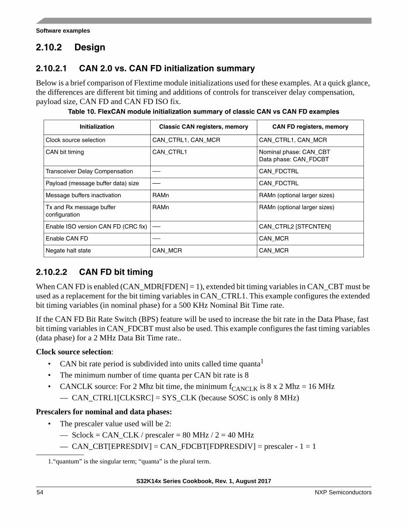
Software examples
2.10.2 Design
2.10.2.1 CAN 2.0 vs. CAN FD initialization summary
Below is a brief comparison of Flextime module initializations used for these examples. At a quick glance, the differences are different bit timing and additions of controls for transceiver delay compensation, payload size, CAN FD and CAN FD ISO fix.
2.10.2.2 CAN FD bit timing
When CAN FD is enabled (CAN_MDR[FDEN] = 1), extended bit timing variables in CAN_CBT must be used as a replacement for the bit timing variables in CAN_CTRL1. This example configures the extended bit timing variables (in nominal phase) for a 500 KHz Nominal Bit Time rate.
If the CAN FD Bit Rate Switch (BPS) feature will be used to increase the bit rate in the Data Phase, fast bit timing variables in CAN_FDCBT must also be used. This example configures the fast timing variables (data phase) for a 2 MHz Data Bit Time rate..
Clock source selection:
• CAN bit rate period is subdivided into units called time quanta1
• The minimum number of time quanta per CAN bit rate is 8
• CANCLK source: For 2 Mhz bit time, the minimum fCANCLK is 8 x 2 Mhz = 16 MHz
— CAN_CTRL1[CLKSRC] = SYS_CLK (because SOSC is only 8 MHz)
Prescalers for nominal and data phases:• The prescaler value used will be 2:
— Sclock = CAN_CLK / prescaler = 80 MHz / 2 = 40 MHz
— CAN_CBT[EPRESDIV] = CAN_FDCBT[FDPRESDIV] = prescaler - 1 = 1
Table 10. FlexCAN module initialization summary of classic CAN vs CAN FD examples
Initialization Classic CAN registers, memory CAN FD registers, memory
Clock source selection CAN_CTRL1, CAN_MCR CAN_CTRL1, CAN_MCR
CAN bit timing CAN_CTRL1 Nominal phase: CAN_CBTData phase: CAN_FDCBT
Transceiver Delay Compensation — CAN_FDCTRL
Payload (message buffer data) size — CAN_FDCTRL
Message buffers inactivation RAMn RAMn (optional larger sizes)
Tx and Rx message buffer configuration
RAMn RAMn (optional larger sizes)
Enable ISO version CAN FD (CRC fix) — CAN_CTRL2 [STFCNTEN]
Enable CAN FD — CAN_MCR
Negate halt state CAN_MCR CAN_MCR
1.“quantum” is the singular term; “quanta” is the plural term.
S32K14x Series Cookbook, Rev. 1, August 2017
NXP Semiconductors54
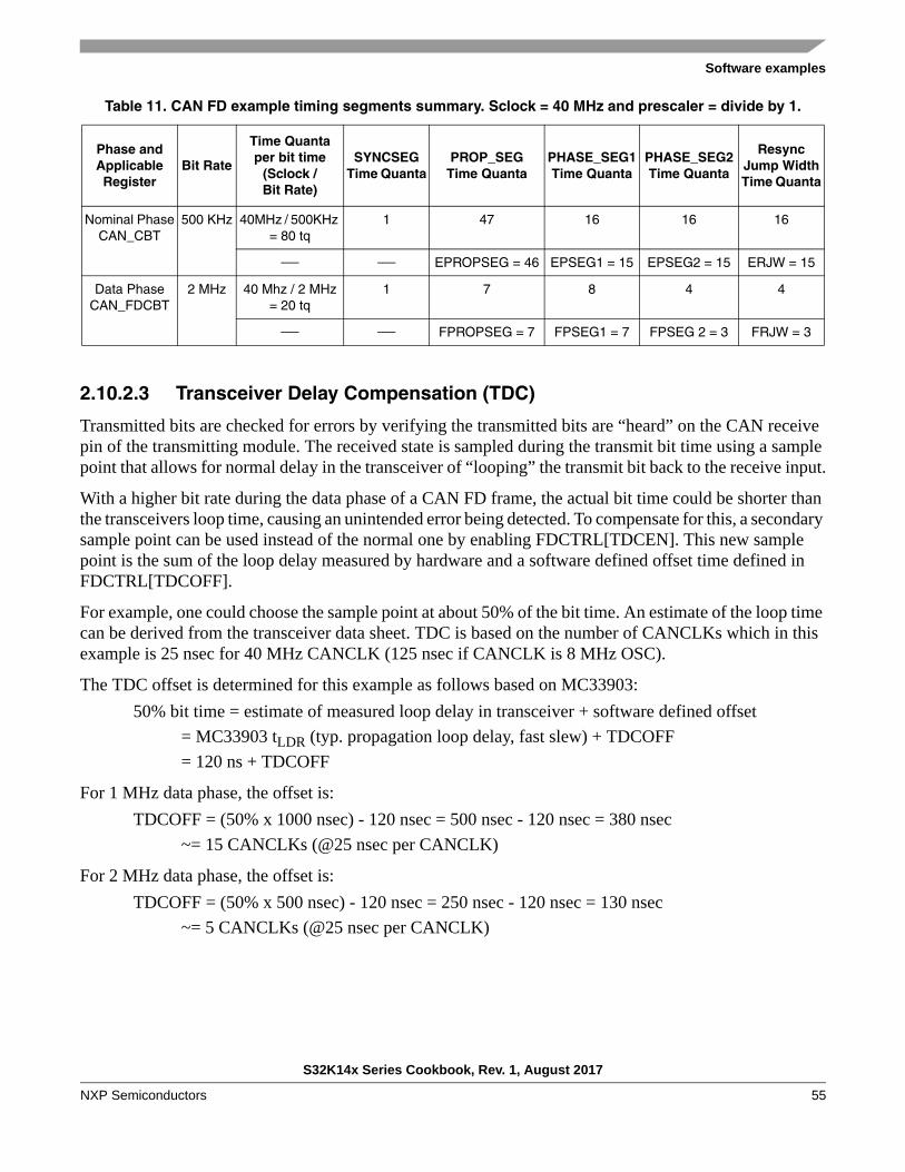
Software examples
2.10.2.3 Transceiver Delay Compensation (TDC)
Transmitted bits are checked for errors by verifying the transmitted bits are “heard” on the CAN receive pin of the transmitting module. The received state is sampled during the transmit bit time using a sample point that allows for normal delay in the transceiver of “looping” the transmit bit back to the receive input.
With a higher bit rate during the data phase of a CAN FD frame, the actual bit time could be shorter than the transceivers loop time, causing an unintended error being detected. To compensate for this, a secondary sample point can be used instead of the normal one by enabling FDCTRL[TDCEN]. This new sample point is the sum of the loop delay measured by hardware and a software defined offset time defined in FDCTRL[TDCOFF].
For example, one could choose the sample point at about 50% of the bit time. An estimate of the loop time can be derived from the transceiver data sheet. TDC is based on the number of CANCLKs which in this example is 25 nsec for 40 MHz CANCLK (125 nsec if CANCLK is 8 MHz OSC).
The TDC offset is determined for this example as follows based on MC33903:
50% bit time = estimate of measured loop delay in transceiver + software defined offset
= MC33903 tLDR (typ. propagation loop delay, fast slew) + TDCOFF
= 120 ns + TDCOFF
For 1 MHz data phase, the offset is:
TDCOFF = (50% x 1000 nsec) - 120 nsec = 500 nsec - 120 nsec = 380 nsec
~= 15 CANCLKs (@25 nsec per CANCLK)
For 2 MHz data phase, the offset is:
TDCOFF = (50% x 500 nsec) - 120 nsec = 250 nsec - 120 nsec = 130 nsec
~= 5 CANCLKs (@25 nsec per CANCLK)
Table 11. CAN FD example timing segments summary. Sclock = 40 MHz and prescaler = divide by 1.
Phase andApplicable Register
Bit Rate
Time Quantaper bit time
(Sclock / Bit Rate)
SYNCSEGTime Quanta
PROP_SEG Time Quanta
PHASE_SEG1 Time Quanta
PHASE_SEG2 Time Quanta
Resync Jump WidthTime Quanta
Nominal PhaseCAN_CBT
500 KHz 40MHz / 500KHz = 80 tq
1 47 16 16 16
— — EPROPSEG = 46 EPSEG1 = 15 EPSEG2 = 15 ERJW = 15
Data PhaseCAN_FDCBT
2 MHz 40 Mhz / 2 MHz = 20 tq
1 7 8 4 4
— — FPROPSEG = 7 FPSEG1 = 7 FPSEG 2 = 3 FRJW = 3
S32K14x Series Cookbook, Rev. 1, August 2017
NXP Semiconductors 55
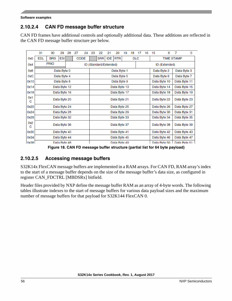
Software examples
2.10.2.4 CAN FD message buffer structure
CAN FD frames have additional controls and optionally additional data. These additions are reflected in the CAN FD message buffer structure per below.
Figure 18. CAN FD message buffer structure (partial list for 64 byte payload)
2.10.2.5 Accessing message buffers
S32K14x FlexCAN message buffers are implemented in a RAM arrays. For CAN FD, RAM array’s index to the start of a message buffer depends on the size of the message buffer’s data size, as configured in register CAN_FDCTRL [MBDSRx] bitfield.
Header files provided by NXP define the message buffer RAM as an array of 4-byte words. The following tables illustrate indexes to the start of message buffers for various data payload sizes and the maximum number of message buffers for that payload for S32K144 FlexCAN 0.
S32K14x Series Cookbook, Rev. 1, August 2017
NXP Semiconductors56

Software examples
asdf
asdf
To access a word in a message buffer, add the index of the start of the message buffer plus an index of the word number in the message buffer:
CANx->RAMn[(index of start of message buffer) + (index of word inside message buffer)]
Example: For 64-byte payload, initialize message buffer 2’s second data word (index value of 3 since header words are indexes 0, 1 and data word is index 2):
CANx->RAMn[(0x24 + 0x3)] = 0x12345678; /* MB2, 2nd data word */
Code can be generalized to access a message buffer’s word using the MBDSRx bitfield. Example#define MBDSR0 3 /* Msg Buffer Data Size for Region 0: 3 (64 bytes or 16 words) */uint32_t msg_buf_size_r0; /* Message Buffer size, region 0, in words */
msg_buf_size_r0 = 2 + exp2(MBDSR0+1); /* Msg Buf Size Reg 0 = 2 hdr + 2**4 data words */
CAN0->RAMn[4*msg_buf_size_r0 + 0] |= 1<<31; /* MB4 word 0: set bit 31, EDL = 1 */
Table 12. S32K144 FlexCAN0: RAMn word index to start of Message Buffer (MB).
RAM Index
(words, 4B each)
8 Bytes Data(MSBDRx = 0)
16 Bytes Data (MSBDRx = 1)
32 Bytes Data (MSBDRx = 2)
64 Bytes Data (MSBDRx = 3)
MB #(32 max.)
FrameMB #
(20 max.)Frame
MB #(11 max.)
FrameMB #
(6 max.)Frame
0x0MB0
8B Hdr.
MB0
8B Hdr.
MB0
8B Hdr.
MB0
8B Hdr.
0x2 8B Data16B Data
32B Data
64B Data
0x4MB1
8B Hdr.
0x8 8B Data
MB1
8B Hdr.
0xAMB2
8B Hdr.16B Data
0xC 8B Data
MB1
8B Hdr.
0xEMB3
8B Hdr.
MB2
8B Hdr.
32B Data
0x10 8B Data16B Data
0x12MB4
8B Hdr.
0x14 8B Data
MB4
8B Hdr.
MB1
8B Hdr.
0x16MB5
8B Hdr.16B Data
MB2
8B Hdr.
64B Data
0x18 8B Data
32B Data
0x1AMB6
8B Hdr.
MB5
8B Hdr.
0x1C 8B Data 16B Data
etc.
Table 13. S32K144 FlexCAN 0: CAN FD maximum number of message buffers
8 Bytes Data(MSBDRx = 0)
16 Bytes Data (MSBDRx = 1)
32 Bytes Data (MSBDRx = 2)
64 Bytes Data (MSBDRx = 3)
32 Message Buffers 21 Message Buffers 12 Message Buffers 7 Message Buffers
S32K14x Series Cookbook, Rev. 1, August 2017
NXP Semiconductors 57
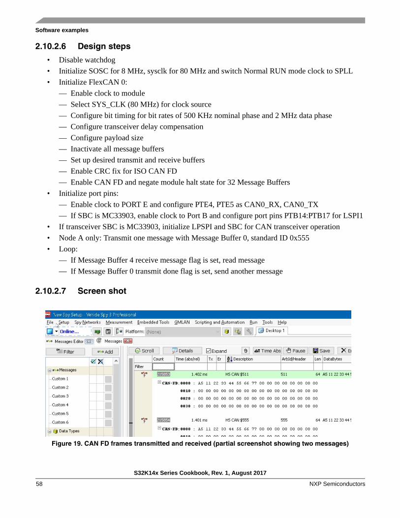
Software examples
2.10.2.6 Design steps
• Disable watchdog
• Initialize SOSC for 8 MHz, sysclk for 80 MHz and switch Normal RUN mode clock to SPLL
• Initialize FlexCAN 0:
— Enable clock to module
— Select SYS_CLK (80 MHz) for clock source
— Configure bit timing for bit rates of 500 KHz nominal phase and 2 MHz data phase
— Configure transceiver delay compensation
— Configure payload size
— Inactivate all message buffers
— Set up desired transmit and receive buffers
— Enable CRC fix for ISO CAN FD
— Enable CAN FD and negate module halt state for 32 Message Buffers
• Initialize port pins:
— Enable clock to PORT E and configure PTE4, PTE5 as CAN0_RX, CAN0_TX
— If SBC is MC33903, enable clock to Port B and configure port pins PTB14:PTB17 for LSPI1
• If transceiver SBC is MC33903, initialize LPSPI and SBC for CAN transceiver operation
• Node A only: Transmit one message with Message Buffer 0, standard ID 0x555
• Loop:
— If Message Buffer 4 receive message flag is set, read message
— If Message Buffer 0 transmit done flag is set, send another message
2.10.2.7 Screen shot
Figure 19. CAN FD frames transmitted and received (partial screenshot showing two messages)
S32K14x Series Cookbook, Rev. 1, August 2017
NXP Semiconductors58
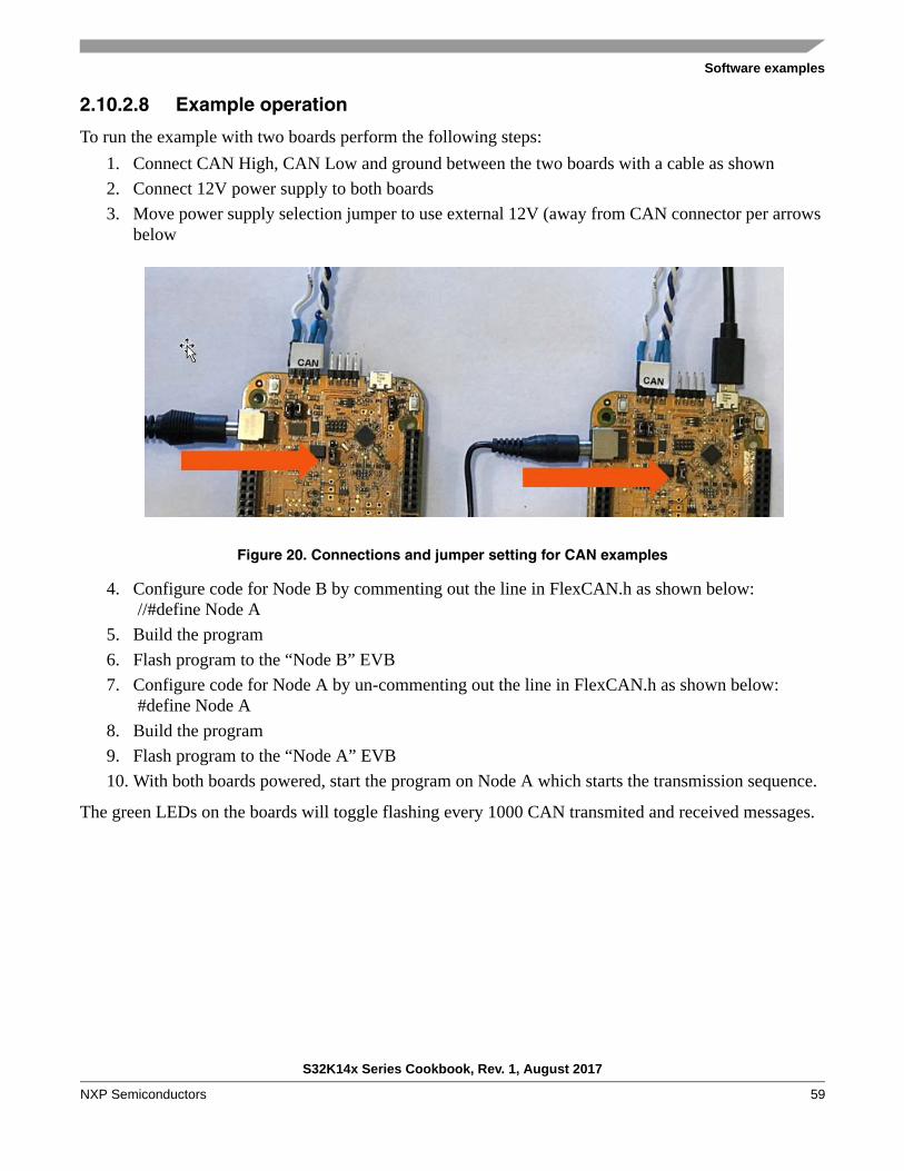
Software examples
2.10.2.8 Example operation
To run the example with two boards perform the following steps:
1. Connect CAN High, CAN Low and ground between the two boards with a cable as shown
2. Connect 12V power supply to both boards
3. Move power supply selection jumper to use external 12V (away from CAN connector per arrows below
Figure 20. Connections and jumper setting for CAN examples
4. Configure code for Node B by commenting out the line in FlexCAN.h as shown below: //#define Node A
5. Build the program
6. Flash program to the “Node B” EVB
7. Configure code for Node A by un-commenting out the line in FlexCAN.h as shown below: #define Node A
8. Build the program
9. Flash program to the “Node A” EVB
10. With both boards powered, start the program on Node A which starts the transmission sequence.
The green LEDs on the boards will toggle flashing every 1000 CAN transmited and received messages.
S32K14x Series Cookbook, Rev. 1, August 2017
NXP Semiconductors 59

Software examples
2.10.3 Code
2.10.3.1 main.c
#include "S32K144.h" /* include peripheral declarations S32K144 */#include "FlexCAN_FD.h"#include "clocks_and_modes.h"void WDOG_disable (void){ WDOG->CNT=0xD928C520; /* Unlock watchdog */ WDOG->TOVAL=0x0000FFFF; /* Maximum timeout value */ WDOG->CS = 0x00002100; /* Disable watchdog */}void PORT_init (void) { PCC->PCCn[PCC_PORTE_INDEX] |= PCC_PCCn_CGC_MASK; /* Enable clock for PORTE */ PORTE->PCR[4] |= PORT_PCR_MUX(5); /* Port E4: MUX = ALT5, CAN0_RX */ PORTE->PCR[5] |= PORT_PCR_MUX(5); /* Port E5: MUX = ALT5, CAN0_TX */ PCC->PCCn[PCC_PORTD_INDEX ]|=PCC_PCCn_CGC_MASK; /* Enable clock for PORTD */ PORTD->PCR[16] = 0x00000100; /* Port D16: MUX = GPIO (to green LED) */ PTD->PDDR |= 1<<16; /* Port D16: Data direction = output */}int main(void) { uint32_t rx_msg_count = 0; uint32_t i = 0; /* dummy delay variable */ WDOG_disable(); SOSC_init_8MHz(); /* Initialize system oscillator for 8 MHz xtal */ SPLL_init_160MHz(); /* Initialize SPLL to 160 MHz with 8 MHz SOSC */ NormalRUNmode_80MHz(); /* Init clocks: 80 MHz sysclk & core, 40 MHz bus, 20 MHz flash */ FLEXCAN0_init(); /* Init FlexCAN0 */ PORT_init(); /* Configure ports */#ifdef NODE_A /* Node A transmits first; Node B transmits after reception */ FLEXCAN0_transmit_msg(); /* Transmit initial message from Node A to Node B */#endif for (;;) { /* Loop: if a msg is received, transmit a msg */ if ((CAN0->IFLAG1 >> 4) & 1) { /* If CAN 0 MB 4 flag is set (received msg), read MB4 */ FLEXCAN0_receive_msg (); /* Read message */ rx_msg_count++; /* Increment receive msg counter */ if (rx_msg_count == 1000) { /* If 1000 messages have been received, */ PTD->PTOR |= 1<<16; /* toggle output port D16 (Green LED) */ rx_msg_count = 0; /* and reset message counter */ } FLEXCAN0_transmit_msg (); /* Transmit message using MB0 */ }
S32K14x Series Cookbook, Rev. 1, August 2017
NXP Semiconductors60

Software examples
}
2.10.3.2 FlexCAN_FD.c
#include "S32K144.h" /* include peripheral declarations S32K144 */#include "FlexCAN_FD.h"
uint32_t RxCODE; /* Received message buffer code */uint32_t RxID; /* Received message ID */uint32_t RxLENGTH; /* Received message number of data bytes */uint32_t RxDATA[2]; /* Received message data (2 words) */uint32_t RxTIMESTAMP; /* Received message time */
void FLEXCAN0_init(void) {#define MSG_BUF_SIZE 18 /* Msg Buffer Size. (2 words hdr + 16 words data = 18 words) */ uint32_t i=0;
PCC->PCCn[PCC_FLEXCAN0_INDEX] |= PCC_PCCn_CGC_MASK; /* CGC=1: enable clock to FlexCAN0 */ CAN0->MCR |= CAN_MCR_MDIS_MASK; /* MDIS=1: Disable module before selecting clock */ CAN0->CTRL1 |= CAN_CTRL1_CLKSRC_MASK; /* CLKSRC=1: Clock Source = BUSCLK (40 MHz) */ CAN0->MCR &= ~CAN_MCR_MDIS_MASK; /* MDIS=0; Enable module config. (Sets FRZ, HALT)*/ while (!((CAN0->MCR & CAN_MCR_FRZACK_MASK) >> CAN_MCR_FRZACK_SHIFT)) {} /* Good practice: wait for FRZACK=1 on freeze mode entry/exit */ CAN0->CBT = 0x802FB9EF; /* Configure nominal phase: 500 KHz bit time, 40 MHz Sclock */ /* Prescaler = CANCLK / Sclock = 80 MHz / 40 MHz = 2 */ /* EPRESDIV = Prescaler - 1 = 2 - 1 = 1 */ /* EPSEG2 = 15 */ /* EPSEG1 = 15 */ /* EPROPSEG = 46 */ /* ERJW = 15 */ /* BITRATEn =Fcanclk /( [(1 + (EPSEG1+1) + (EPSEG2+1) + (EPROPSEG + 1)] x (EPRESDIV+1)) */ /* = 80 MHz /( [(1 + ( 15 +1) + ( 15 +1) + ( 46 + 1)] x ( 1 +1)) */ /* = 80 MHz /( [1+16+16+47] x 2) = 80 MHz /(80x2) = 500 Kz */
CAN0->FDCBT = 0x00131CE3; /* Configure data phase: 2 MHz bit time, 40 MHz Sclock */ /* Prescaler = CANCLK / Sclock = 80 MHz / 40 MHz = 2 */ /* FPRESDIV = Prescaler - 1 = = 2 - 1 = 1 */ /* FPSEG2 = 3 */ /* FPSEG1 = 7 */ /* FPROPSEG = 7 */ /* FRJW = 3 */ /* BITRATEf =Fcanclk /( [(1 + (FPSEG1+1) + (FPSEG2+1) + (FPROPSEG)] x (FPRESDIV+!)) */ /* = 80 MHz /( [(1 + ( 7 +1) + ( 3 +1) + ( 7 )] x ( 1 +1)) */
S32K14x Series Cookbook, Rev. 1, August 2017
NXP Semiconductors 61

Software examples
/* = 80 MHz /( [1+8+4+7] x 2) = 80 MHz /(20x2) = 80 MHz / 40 = 2 MHz */ CAN0->FDCTRL =0x80038500; /* Configure bit rate switch, data size, transcv'r delay */ /* BRS=1: enable Bit Rate Swtich in frame's header */ /* MBDSR1: Not applicable */ /* MBDSR0=3: Region 0 has 64 bytes data in frame's payload */ /* TDCEN=1: enable Transceiver Delay Compensation */ /* TDCOFF=5: 5 CAN clocks (300us) offset used */ for(i=0; i<128; i++ ) { /* CAN0: clear 128 words RAM in FlexCAN 0 */ CAN0->RAMn[i] = 0; /* Clear msg buf words. All buffers CODE=0 (inactive) */ } for(i=0; i<16; i++ ) { /* In FRZ mode, init CAN0 16 msg buf filters */ CAN0->RXIMR[i] = 0xFFFFFFFF; /* Check all ID bits for incoming messages */ } CAN0->RXMGMASK = 0x1FFFFFFF; /* Global acceptance mask: check all ID bits */ /* Message Buffer 4 - receive setup: */ CAN0->RAMn[ 4*MSG_BUF_SIZE + 0] = 0xC4000000; /* Msg Buf 4, word 0: Enable for reception */ /* EDL=1: Extended Data Length for CAN FD */ /* BRS = 1: Bit Rate Switch enabled */ /* ESI = 0: Error state */ /* CODE=4: MB set to RX inactive */ /* IDE=0: Standard ID */ /* SRR, RTR, TIME STAMP = 0: not applicable */#ifdef NODE_A /* Node A receives msg with std ID 0x511 */ CAN0->RAMn[ 4*MSG_BUF_SIZE + 1] = 0x14440000; /* Msg Buf 4, word 1: Standard ID = 0x111 */#else /* Node B to receive msg with std ID 0x555 */ CAN0->RAMn[ 4*MSG_BUF_SIZE + 1] = 0x15540000; /* Msg Buf 4, word 1: Standard ID = 0x555 */#endif /* PRIO = 0: CANFD not used */ CAN0->CTRL2 |= CAN_CTRL2_STFCNTEN_MASK; /* Enable CRC fix for ISO CAN FD */ CAN0->MCR = 0x0000081F; /* Negate FlexCAN 1 halt state & enable CAN FD for 32 MBs */ while ((CAN0->MCR && CAN_MCR_FRZACK_MASK) >> CAN_MCR_FRZACK_SHIFT) {} /* Good practice: wait for FRZACK to clear (not in freeze mode) */ while ((CAN0->MCR && CAN_MCR_NOTRDY_MASK) >> CAN_MCR_NOTRDY_SHIFT) {} /* Good practice: wait for NOTRDY to clear (module ready) */}
S32K14x Series Cookbook, Rev. 1, August 2017
NXP Semiconductors62
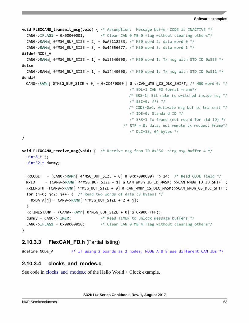
Software examples
void FLEXCAN0_transmit_msg(void) { /* Assumption: Message buffer CODE is INACTIVE */ CAN0->IFLAG1 = 0x00000001; /* Clear CAN 0 MB 0 flag without clearing others*/ CAN0->RAMn[ 0*MSG_BUF_SIZE + 2] = 0xA5112233; /* MB0 word 2: data word 0 */ CAN0->RAMn[ 0*MSG_BUF_SIZE + 3] = 0x44556677; /* MB0 word 3: data word 1 */#ifdef NODE_A CAN0->RAMn[ 0*MSG_BUF_SIZE + 1] = 0x15540000; /* MB0 word 1: Tx msg with STD ID 0x555 */#else CAN0->RAMn[ 0*MSG_BUF_SIZE + 1] = 0x14440000; /* MB0 word 1: Tx msg with STD ID 0x511 */#endif CAN0->RAMn[ 0*MSG_BUF_SIZE + 0] = 0xCC4F0000 | 8 <<CAN_WMBn_CS_DLC_SHIFT; /* MB0 word 0: */ /* EDL=1 CAN FD format frame*/ /* BRS=1: Bit rate is switched inside msg */ /* ESI=0: ??? */ /* CODE=0xC: Activate msg buf to transmit */ /* IDE=0: Standard ID */ /* SRR=1 Tx frame (not req'd for std ID) */ /* RTR = 0: data, not remote tx request frame*/ /* DLC=15; 64 bytes */}
void FLEXCAN0_receive_msg(void) { /* Receive msg from ID 0x556 using msg buffer 4 */ uint8_t j; uint32_t dummy;
RxCODE = (CAN0->RAMn[ 4*MSG_BUF_SIZE + 0] & 0x07000000) >> 24; /* Read CODE field */ RxID = (CAN0->RAMn[ 4*MSG_BUF_SIZE + 1] & CAN_WMBn_ID_ID_MASK) >>CAN_WMBn_ID_ID_SHIFT ; RxLENGTH =(CAN0->RAMn[ 4*MSG_BUF_SIZE + 0] & CAN_WMBn_CS_DLC_MASK)>>CAN_WMBn_CS_DLC_SHIFT; for (j=0; j<2; j++) { /* Read two words of data (8 bytes) */ RxDATA[j] = CAN0->RAMn[ 4*MSG_BUF_SIZE + 2 + j]; } RxTIMESTAMP = (CAN0->RAMn[ 0*MSG_BUF_SIZE + 0] & 0x000FFFF); dummy = CAN0->TIMER; /* Read TIMER to unlock message buffers */ CAN0->IFLAG1 = 0x00000010; /* Clear CAN 0 MB 4 flag without clearing others*/}
2.10.3.3 FlexCAN_FD.h (Partial listing)
#define NODE_A /* If using 2 boards as 2 nodes, NODE A & B use different CAN IDs */
2.10.3.4 clocks_and_modes.c
See code in clocks_and_modes.c of the Hello World + Clock example.
S32K14x Series Cookbook, Rev. 1, August 2017
NXP Semiconductors 63
Software examples
2.10.3.5 Reference: MC33903 code for obsolete EVB (not included in project)
LPSPI1 initialization, transmit and receiver functions: See code for functions in SPI example.
Port pin and MC33803 initialization: See code for functions in CAN 2.0 example.
CAN initialization for 1 MHz data phase (MC33903 limit):
/* Use 1 MHz data phase bit rate for MC33903:*/ CAN0->FDCBT = 0x00135CE7; /* Configure data phase: 1 MHz bit time, 40 MHz Sclock */ /* Prescaler = CANCLK / Sclock = 80 MHz / 40 MHz = 2 */ /* FPRESDIV = Prescaler - 1 = 2 - 1 = 1 */ /* FPSEG2 = 7 */ /* FPSEG1 = 7 */ /* FPROPSEG = 23 */ /* FRJW = 3 */ /* BITRATEf =Fcanclk /( [(1 + (FPSEG1+1) + (FPSEG2+1) + (FPROPSEG)] x (FPRESDIV+!)) */ /* = 80 MHz /( [(1 + ( 7 +1) + ( 7 +1) + ( 23 )] x ( 1 +1)) */ /* = 80 MHz /( [1+8+8+23] x 2) = 80 MHz /(40x2) = 80 MHz / 80 = 1 MHz */ CAN0->FDCTRL = 0x8003F300; /* Configure bit rate switch, data size, transcv'r delay */ /* BRS=1: enable Bit Rate Swtich in frame's header */ /* MBDSR1: Not applicable */ /* MBDSR0=3: Region 0 has 64 bytes data in frame's payload */ /* TDCEN=1: enable Transceiver Delay Compensation */ /* TDCOFF=15: 15 CAN clocks (375us) offset used */
S32K14x Series Cookbook, Rev. 1, August 2017
NXP Semiconductors64

Startup code
3 Startup code
3.1 S32 Design Studio, S32K14x flash targetCompiler normally have wizards or sample startup code which include initializations such as listed below. In general, this code should be considered as a starting point. Users should review the initializations to see if any are missing or if changes are desired.
Other common startup functions include:
• Cache
— S32K144 has a 4 KB instruction cache, 2-way set associative, four word lines
— Software can configure the MPU to define cachable and non cachable areas of flash.
— Software must invalidate and enable cache. Example1:LMEM->PCCCR = 0x85000001; /* Invalidate cache & enable write buffer, cache */
• Flash Controller
— Prefetch buffers perform speculative reads to increase performance for sequential accesses
— Software must enable prefetch buffers. Example2:MSCM->OCMDR0 = 0x00000020; /* Bit 5 = 1: Enable program flash prefetch buffer */MSCM->OCMDR1 = 0x00000020; /* Bit 5 = 1: Enable data flash prefetch buffer */
Table 14. Start up code summary for S32 Design Studio v1.2, S32K144, flash target.
Step startup_S32K144.s system_S32K144.h system_S32K144.c startup.c
1 __isr_vector table, per link file starts at 0x0, defines:- 0x0 __StackTop address,- 0x4 Reset_Handler address,- other exception addresses,- interrupt vector addresses
2 Reset_Handler:- Masks interrupts- Initializes regs, SP, - SystemInit
3 DISABLE_WDOG = 1 SystemInit:- disable watchdog
4 init_data_bss
5 init_data_bss:- Init vector table- Init data pointers, .data etc.- Copy init data ROM to RAM- Init .bss
6 Branch to main
1.S32K14x SertiesRreference Manual, Rev. 1, 08/2016, section 29.4.4.1 Cache set commands2.S32K14x SertiesRreference Manual, Rev. 1, 08/2016, section 31.5.2 Speculative reads
S32K14x Series Cookbook, Rev. 1, August 2017
NXP Semiconductors 65
Header files cheat sheet
InR
InB
S
C
R
RF
4 Header files cheat sheetTable 15. Header files cheat sheet
Action Family Syntax Examples
itialize egister
S12 MODULEREG = value; CPMUPOSTDIV = 0;
MPC5xxx MODULE.REG.R = value; SIUL.PCR[40].R = 0x1234;
KEA MODULE_REG = value; FTM2_C0SC = 0X68;
S32K MODULE->REG = value; PORTD->PCR[10] = 0X00000200;
itialize it Field
S12 MODULEREG_FIELD = value; CPMUPLL_FM = 2;
MPC5xxx MODULE.REG.B.FIELD = value; SIUL.PCR[4].B.PA = 3;
KEA MODULEn-_REG &= ~MOD_REG_FIELD_MASK;and MODULEn-_REG |= MOD_REG_FIELD(value);
ADC_SC1 &= ~ADC_SC1_ADCH_MASK; // clear fieldADC_SC1 |= ADC_SC1_ADCH(6); // initialize field
S32K MODULEn-->REG &= MODULE_REG_FIELD_MASK;MODULEn-->REG = MODULE_REG_FIELD(value);
PORTE->PCR[4] &= ~PORT_PCR_MUX_MASK; PORTE->PCR[4] |= PORT_PCR_MUX(0b010);
et Bit S12 MODULEREG_FIELD = 1; CPMURTI_RTDEC = 1;
MPC5xxx MODULE[n].REG.B.FIELD = 1; SIUL.PCR[40].B.OBE = 1;
KEA MODULEn-_REG |= MODULE_REG_FIELD_MASK;or MODULEn-_REG |= 1<<CONSTANT;
SIM_SCGC |= SIM_SCGC_FM2_MASK;#define PTC0 9;GPIOA_PDDR |= 1<<PTC0;
S32K MODULEn-->REG |= MODULE_REG_FIELD_MASK;or MODULEn-->REG |= 1<<CONSTANT;
LPIT0->MCR |= LPIT_MCR_CEN_MASK;PTD->PDDR |= 1<<10;
lear Bit S12 MODULEREG_FIELD = 0; CPMURTI_RTDEC = 0;
MPC5xxx MODULE.REG.B.FIELD = 0; SIUL.PCR[40].B.OBE = 0;
KEA MODULEn-_REG &= ~MODULE_REG_FIELD_MASK;or MODULEn-_REG &= ~(1<<CONSTANT);
I2C_C1 &= ~I2C_C1_TX_MASK;GPIOA_PDDR &= ~(1<<12);
S32K MODULEn->REG &= ~MODULE_REG_FIELD_MASK;or MODULEn-->REG &= ~(1<<CONSTANT); PTC->PDDR &= ~(1<<12);
ead Bit S12 x = MODULEREG_FIELD; x = CPMURTI_RTDEC;
MPC5xxx x = MODULE.REG.B.FIELD; x = SIUL.PCR[5].B.OBE;
KEA x = (MODULEn-_REG>>CONSTANT) & 1; x = (GPIOA_PIDR>>PTD0) & 1;
S32K x = (MODULEn-->REG>>CONSTANT) & 1; x = (LPSPI1->SR & LPSPI_SR_TDF_MASK)>>LPSPI_SR_TDF_SHIFT
ead Bit ield
S12 x = MODULEREG_FIELD; x = CPMUSYNR_SYNDIV;
MPC5xxx x = MODULE.REG.B.FIELD; x = SIUL.PCR[5].B.PA;
KEA x = (MODULEn-_REG & MODULE_REG_FIELD_MASK) >> MODULE_REG_FIELD_SHIFT;
x = (I2C_A1 & I2C_A1_AD_MASK) >> I2C_A1_AD_MASK;
S32K x = (MODULEn-->REG & MODULE_REG_FIELD_MASK) >> MODULE_REG_FIELD_SHIFT;
x = (LPSPI1->SR & LPSPI_SR_TDF_MASK)>>LPSPI_SR_TDF_SHIFT
S32K14x Series Cookbook, Rev. 1, August 2017
NXP Semiconductors66
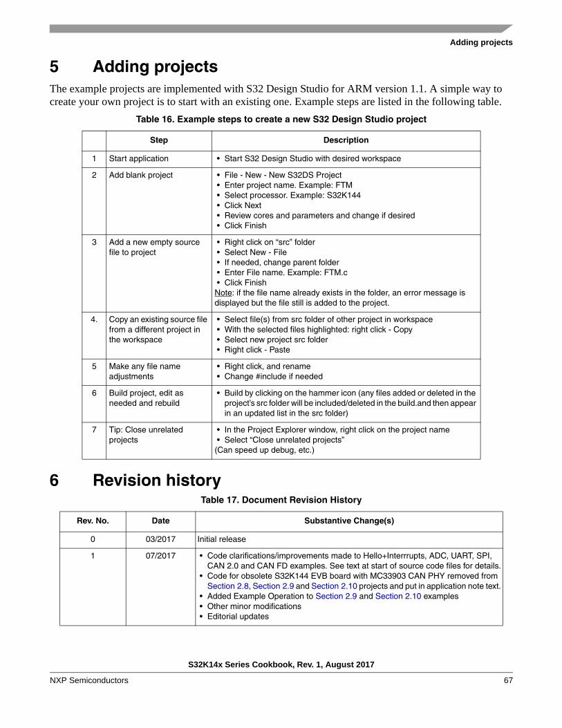
Adding projects
5 Adding projects The example projects are implemented with S32 Design Studio for ARM version 1.1. A simple way to create your own project is to start with an existing one. Example steps are listed in the following table.
6 Revision history
Table 16. Example steps to create a new S32 Design Studio project
Step Description
1 Start application • Start S32 Design Studio with desired workspace
2 Add blank project • File - New - New S32DS Project • Enter project name. Example: FTM • Select processor. Example: S32K144 • Click Next • Review cores and parameters and change if desired • Click Finish
3 Add a new empty source file to project
• Right click on “src” folder • Select New - File • If needed, change parent folder • Enter File name. Example: FTM.c • Click FinishNote: if the file name already exists in the folder, an error message is displayed but the file still is added to the project.
4. Copy an existing source file from a different project in the workspace
• Select file(s) from src folder of other project in workspace • With the selected files highlighted: right click - Copy • Select new project src folder • Right click - Paste
5 Make any file name adjustments
• Right click, and rename • Change #include if needed
6 Build project, edit as needed and rebuild
• Build by clicking on the hammer icon (any files added or deleted in the project’s src folder will be included/deleted in the build.and then appear in an updated list in the src folder)
7 Tip: Close unrelated projects
• In the Project Explorer window, right click on the project name • Select “Close unrelated projects”(Can speed up debug, etc.)
Table 17. Document Revision History
Rev. No. Date Substantive Change(s)
0 03/2017 Initial release
1 07/2017 • Code clarifications/improvements made to Hello+Interrrupts, ADC, UART, SPI, CAN 2.0 and CAN FD examples. See text at start of source code files for details.
• Code for obsolete S32K144 EVB board with MC33903 CAN PHY removed from Section 2.8, Section 2.9 and Section 2.10 projects and put in application note text.
• Added Example Operation to Section 2.9 and Section 2.10 examples • Other minor modifications • Editorial updates
S32K14x Series Cookbook, Rev. 1, August 2017
NXP Semiconductors 67
Document Number: AN5413Rev. 108/2017
Information in this document is provided solely to enable system and software
implementers to use NXP products. There are no express or implied copyright
licenses granted hereunder to design or fabricate any integrated circuits based
on the information in this document. NXP reserves the right to make changeswithout further notice to any products herein.
NXP makes no warranty, representation, or guarantee regarding the suitability of
its products for any particular purpose, nor does NXP assume any liability arising
out of the application or use of any product or circuit, and specifically disclaims
any and all liability, including without limitation consequential or incidental
damages. “Typical” parameters that may be provided in NXP data sheets and/or
specifications can and do vary in different applications, and actual performance
may vary over time. All operating parameters, including “typicals,” must be
validated for each customer application by customers technical experts. NXP
does not convey any license under its patent rights nor the rights of others. NXP
sells products pursuant to standard terms and conditions of sale, which can befound at the following address: nxp.com/SalesTermsandConditions.
How to Reach Us:Home Page: nxp.com
Web Support: nxp.com/support
NXP, the NXP logo, NXP SECURE CONNECTIONS FOR A SMARTER
WORLD, COOLFLUX, EMBRACE, GREENCHIP, HITAG, I2C BUS, ICODE,
JCOP, LIFE VIBES, MIFARE, MIFARE CLASSIC, MIFARE DESFire, MIFARE
PLUS, MIFARE FLEX, MANTIS, MIFARE ULTRALIGHT, MIFARE4MOBILE,
MIGLO, NTAG, ROADLINK, SMARTLX, SMARTMX, STARPLUG, TOPFET,
TRENCHMOS, UCODE, Freescale, the Freescale logo, AltiVec, C-5, CodeTest,
CodeWarrior, ColdFire, ColdFire+, C-Ware, the Energy Efficient Solutions logo,
Kinetis, Layerscape, MagniV, mobileGT, PEG, PowerQUICC, Processor Expert,
QorIQ, QorIQ Qonverge, Ready Play, SafeAssure, the SafeAssure logo,
StarCore, Symphony, VortiQa, Vybrid, Airfast, BeeKit, BeeStack, CoreNet,
Flexis, MXC, Platform in a Package, QUICC Engine, SMARTMOS, Tower,
TurboLink, and UMEMS are trademarks of NXP B.V. All other product or service
names are the property of their respective owners. Arm, AMBA, Arm Powered,
Artisan, Cortex, Jazelle, Keil, SecurCore, Thumb, TrustZone, and ìVision are
registered trademarks of Arm Limited (or its subsidiaries) in the EU and/or
elsewhere. Arm7, Arm9, Arm11, big.LITTLE, CoreLink, CoreSight, DesignStart,
Mali, Mbed, NEON, POP, Sensinode, Socrates, ULINK and Versatile are
trademarks of Arm Limited(or its subsidiaries) in the EU and/or
elsewhere. All rights reserved. Oracle and Java are registered trademarks of
Oracle and/or its affiliates. The Power Architecture and Power.org word marks
and the Power and Power.org logos and related marks are trademarks and
service marks licensed by Power.org.
© 2017 NXP B.V.