S Sppeecciiffiiccaattiioonnss FFoorr AApppprroovvaall Humidity 10 ~ 90%, noncondensing . ... Input...
30
Page 1 of 30 The information within this specification is highly confidential and cannot be shared with anyone except those people covered under NDA who are needed to provide input to the design and production of samples. Confidential S S S p p p e e e c c c i i i f f f i i i c c c a a a t t t i i i o o o n n n s s s F F F o o o r r r A A A p p p p p p r r r o o o v v v a a a l l l Product: 1.79” QCIF+ TFT LCM Model No.: Customer: Approval Customer 200 . . . 200 . . . 200 . . . 200 . . . countersignature countersignature countersignature countersignature Sign Sign Sign Sign Status: Revision 0.0 July 16, 2007
Transcript of S Sppeecciiffiiccaattiioonnss FFoorr AApppprroovvaall Humidity 10 ~ 90%, noncondensing . ... Input...

Page 1 of 30 The information within this specification is highly confidential and cannot be shared with anyone except those people covered under NDA who are needed to provide input to the design and production of samples.
Confidential
SSSpppeeeccciiifffiiicccaaatttiiiooonnnsss FFFooorrr AAApppppprrrooovvvaaalll
Product: 1.79” QCIF+ TFT LCM Model No.: Customer:
Approval Customer
200 . . . 200 . . . 200 . . . 200 . . .
countersignature countersignature countersignature countersignature
Sign Sign Sign Sign
Status: Revision 0.0 July 16, 2007

Revision 0.0 July 16, 2007
Page 2 of 30
Confidential
Contents Revision History ----------------------- (3) 1. General description ----------------------- (4) 2. Module Block Diagram ----------------------- (5) 3. Electrical Requirements ----------------------- (6)
3.1 Absolute Maximum Ratings 3.2 Electrical Characteristics 3.3 Input Pin Connections 3.4 AC Characteristics 3.5 Basic Color and Gray Scales
4. Optical Requirements ----------------------- (11) 4.1 Optical Specifications (Main AMLCD) 5. Qualification ----------------------- (15) 5.1 Inspection condition 5.2 Inspection Method (Sampling) 5.3 Inspection Category 5.4 Visual Inspection 5.5 Electrical Inspection 6. Reliability ----------------------- (23) 8.1 Items of reliability 7. Handling ----------------------- (24) 7.1 Handling 7.2 Handling and cleaning of LCD 7.3 Electrostatic shielding 7.4 Packing 7.5 Layout and How to use 7.6 Safekeeping 7.7 Safety 8. Mechanical Drawings ----------------------- (26) 9. Tray Drawings ----------------------- (27) 10. BOX Drawings ----------------------- (28) 11. FPC Circuit ----------------------- (29) 11. Part list ----------------------- (30)

Revision 0.0 July 16, 2007
Page 3 of 30
Confidential
REVISION HISTORY REV REVISION ITEM DATE
0 Initial version July 12, 2007

Revision 0.0 July 16, 2007
Page 4 of 30
Confidential
1. GENERAL DESCRIPTION: This product is a single display module, which has the color transmissive AMLCD(Active Matrix Liquid Crystal Display) as a main display. This model is composed of the TFT-LCD module, driver circuit and white LED back light unit. The general display module specifications are provided in Table 1.1.1
Table 1.1.1 : General Display Module Specifications Category Parameter Specification
Main LCD Display mode a-Si TFT AMLCD
Display type Transmissive
Display colors 65K & 262K
Active area 28.512mm(H) x 35.64mm(V)
Viewing area 32.4mm(H) x 39.82mm(V)
Number of pixels 176(H) x 220(V)
Pixel arrangement RGB stripe
Pixel size 0.054mm(H) x 0.162mm(V)
Display mode Normally White
Viewing Direction 12 O’clock
Panel F108GJ-1TU (CHI MEI)
LCD Driver LGDP4522 (LG)
Mechanical Overall Dimensions 35mm(H) x 59.23(V) x 2.85T
Backlight LED Backlight 3 White LED’s(1way)
Environmental Operating Temperature -20°C ~ 70°C
Operating Humidity 10 ~ 90%, noncondensing
Revision 0.0 July 16, 2007
Page 5 of 30
Confidential
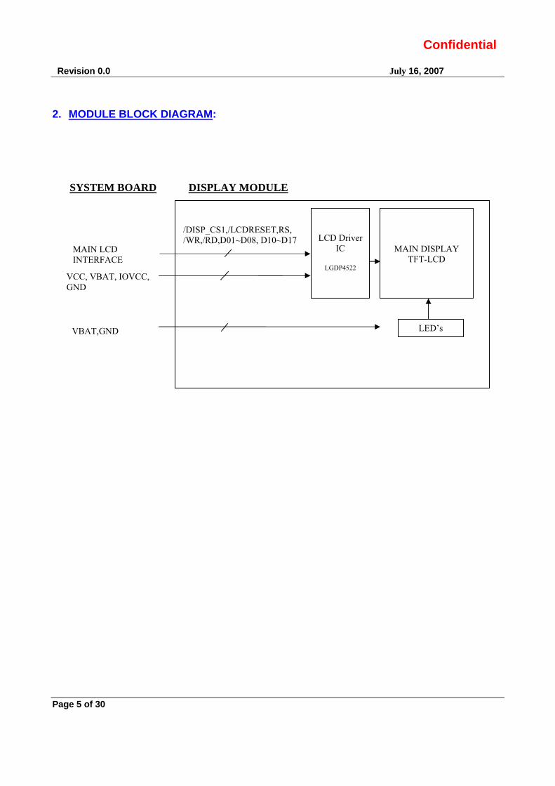
2. MODULE BLOCK DIAGRAM:
MAIN DISPLAY TFT-LCD
LCD Driver IC
LGDP4522
LED’s
/DISP_CS1,/LCDRESET,RS, /WR,/RD,D01~D08, D10~D17
VCC, VBAT, IOVCC, GND
MAIN LCD INTERFACE
VBAT,GND
SYSTEM BOARD DISPLAY MODULE

Revision 0.0 July 16, 2007
Page 6 of 30
Confidential
3. ELECTRICAL REQUIREMENTS:
3.1 Absolute Maximum Ratings: Table 3.1.1: Absolute Maximum Ratings
Parameter Symbol Condition Rating Unit Remarks Power supply (digital) VDD Ta=25°C -0.3 ~ + 3.0 V Note 1 Input voltage (digital) VID Ta=25°C -0.3 ~ + 3.3 V Note 1 Operating temperature T opr -- -40 ~ + 85 °C Storage temperature T stg -55 ~ +125 °C
Note 1: If used beyond the absolute maximum ratings, the LSI may permanentiy be damaged.
It is strongly recommened to use the LSI at a condition within the electrical characteristics for normal operation.
3.2 Electrical Characteristics:
Table 3.2.1: Operating Conditions Parameter Symbol Minimum Typical Maximum Unit Remarks Supply voltage VDD +2.4 +2.8 +3.3 V Battery voltage VBATT +9.0 +9.9 +10.5 V Input voltage - (High) VIH 0.8IOVcc -- IOVCC V Input voltage - (Low) VIL -0.3 -- 0.2IOVcc V
Table 3.2.2: Current Consumption Category Parameter Symbol Minimum Typical Maximum Unit Remarks
Main display
Stand by ISTB - 1.4 10 uA
Sleep ISLP - - 0.1 mA
Still ISTL - 4.0 6.0 mA
Full IF - 8.0 10 mA
Table 3.2.3: Backlight Current consumption Parameter Symbol Minimum Typical Maximum Unit Remarks
Current IB - 15 mA note 1 Power Consumption PBL - 149 mW note 2
Note 1 : Three LEDs are connected in series Note 2 : Where IB = 15mA , VB = PBL / IB

Revision 0.0 July 16, 2007
Page 7 of 30
Confidential
3.3 Input Pin Connections
Pin No. Symbol I/O Function 1 BL_K - Ground 2 BL_A I Battery voltage 3 IOVCC I Supply voltage 4 NC - - 5 RESET I RESET 6 DB17 I/O Data17 7 DB16 I/O Data16 8 DB15 I/O Data15 9 DB14 I/O Data14 10 DB13 I/O Data13 11 DB12 I/O Data12 12 DB11 I/O Data11 13 DB10 I/O Data10 14 NC - - 15 DB08 I/O Data8 16 DB07 I/O Data7 17 DB06 I/O Data6 18 DB05 I/O Data5 19 DB04 I/O Data4 20 DB03 I/O Data3 21 DB02 I/O Data2 22 DB01 I/O Data1 23 NC - - 24 RD I Read 25 WR I Write/read 26 RS I Select Register 27 CS I Chip select 28 VCC I Supply voltage 29 GND I Ground
Revision 0.0 July 16, 2007
Page 8 of 30
Confidential
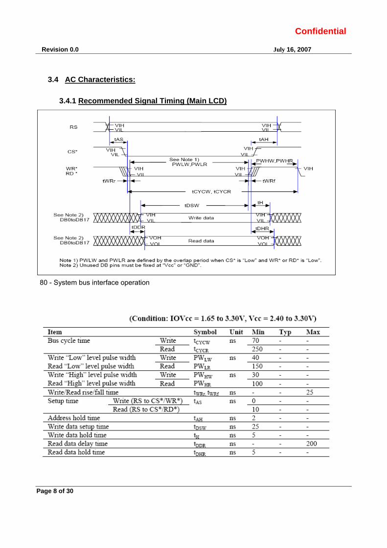
3.4 AC Characteristics:
3.4.1 Recommended Signal Timing (Main LCD)
80 - System bus interface operation
Revision 0.0 July 16, 2007
Page 9 of 30
Confidential
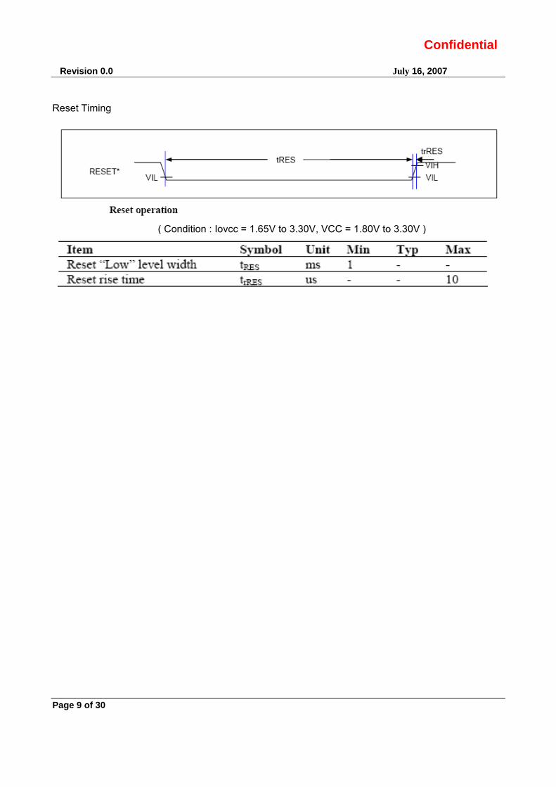
Reset Timing
( Condition : Iovcc = 1.65V to 3.30V, VCC = 1.80V to 3.30V )
Revision 0.0 July 16, 2007
Page 10 of 30
Confidential
3.4.2 Basic Colors and Gray Scales: Table 3.4.1 provides a truth table defining the basic display colors and gray scales available in the main AMLCD. A maximum of 262k colors is possible.
Table 3.4.2: Signals, Basic Display Colors, and Gray Scales – TFT LCD
Colors & Gray Scale
Gray scale
Levels
Data Signal R0
R1
R2
R3
R4
R5
G0
G1
G2
G3
G4
G5
B0
B1
B2
B3
B4
B5
Black -- 0 0 0 0 0 0 0 0 0 0 0 0 0 0 0 0 0 0Blue -- 0 0 0 0 0 0 0 0 0 0 0 0 1 1 1 1 1 1
Green -- 0 0 0 0 0 0 1 1 1 1 1 1 0 0 0 0 0 0Cyan -- 0 0 0 0 0 0 1 1 1 1 1 1 1 1 1 1 1 1Red -- 1 1 1 1 1 1 0 0 0 0 0 0 0 0 0 0 0 0
Magenta -- 1 1 1 1 1 1 0 0 0 0 0 0 1 1 1 1 1 1Yellow -- 1 1 1 1 1 1 1 1 1 1 1 1 0 0 0 0 0 0White -- 1 1 1 1 1 1 1 1 1 1 1 1 1 1 1 1 1 1Black GS0 0 0 0 0 0 0 0 0 0 0 0 0 0 0 0 0 0 0⇑
Darker ⇑ ⇓
Brighter ⇓
GS1 1 0 0 0 0 0 0 0 0 0 0 0 0 0 0 0 0 0GS2 0 1 0 0 0 0 0 0 0 0 0 0 0 0 0 0 0 0↓ ↓ ↓ ↓ ↓ ↓ ↓ ↓
GS29 1 0 1 1 1 1 0 0 0 0 0 0 0 0 0 0 0 0GS30 0 1 1 1 1 1 0 0 0 0 0 0 0 0 0 0 0 0
Red GS31 1 1 1 1 1 1 0 0 0 0 0 0 0 0 0 0 0 0Black GS0 0 0 0 0 0 0 0 0 0 0 0 0 0 0 0 0 0 0⇑
Darker ⇑ ⇓
Brighter ⇓
GS1 0 0 0 0 0 0 1 0 0 0 0 0 0 0 0 0 0 0GS2 0 0 0 0 0 0 0 1 0 0 0 0 0 0 0 0 0 0↓ ↓ ↓ ↓ ↓ ↓ ↓ ↓
GS61 0 0 0 0 0 0 1 0 1 1 1 1 0 0 0 0 0 0GS62 0 0 0 0 0 0 0 1 1 1 1 1 0 0 0 0 0 0
Green GS63 0 0 0 0 0 0 1 1 1 1 1 1 0 0 0 0 0 0Black GS0 0 0 0 0 0 0 0 0 0 0 0 0 0 0 0 0 0 0⇑
Darker ⇑ ⇓
Brighter ⇓
GS1 0 0 0 0 0 0 0 0 0 0 0 0 1 0 0 0 0 0GS2 0 0 0 0 0 0 0 0 0 0 0 0 0 1 0 0 0 0↓ ↓ ↓ ↓ ↓ ↓ ↓ ↓
GS29 0 0 0 0 0 0 0 0 0 0 0 0 1 0 1 1 1 1GS30 0 0 0 0 0 0 0 0 0 0 0 0 0 1 1 1 1 1
Blue GS31 0 0 0 0 0 0 0 0 0 0 0 0 1 1 1 1 1 1 Note 1: In Table 3.4: 0 = Logic low, 1 = Logic high.
Revision 0.0 July 16, 2007
Page 11 of 30
Confidential
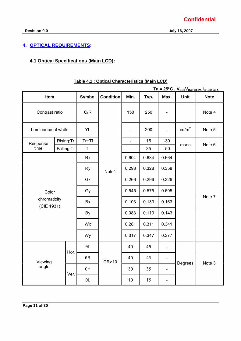
4. OPTICAL REQUIREMENTS:
4.1 Optical Specifications (Main LCD):
Table 4.1 : Optical Characteristics (Main LCD)
Ta = 25°C , VDD=VBAT=3.3V, IBKL=15mA
Item Symbol Condition Min. Typ. Max. Unit Note
Contrast ratio C/R
Note1
150 250 - Note 4
Luminance of white YL - 200 - cd/m2 Note 5
Response time
Rising:Tr Tr+Tf - 15 -30 msec Note 6
Falling:Tf Tf - 35 -50
Color
chromaticity (CIE 1931)
Rx 0.604 0.634 0.664
Note 7
Ry 0.298 0.328 0.358
Gx 0.266 0.296 0.326
Gy 0.545 0.575 0.605
Bx 0.103 0.133 0.163
By 0.083 0.113 0.143
Wx 0.281 0.311 0.341
Wy 0.317 0.347 0.377
Viewing angle
Hor. θL
CR>10
40 45 -
Degrees Note 3 θR 40 45 -
Ver.
θH 30 35 -
θL 10 15 -

Revision 0.0 July 16, 2007
Page 12 of 30
Confidential
Note 1 Measurement should be executed in a stable, windless, and dark room. 30 min after lighting the Back-light. This should be measured on the center of screen. Environment condition: Ta = 25 ± 2 ℃ Back-light ON condition
Back-light OFF condition

Revision 0.0 July 16, 2007
Page 13 of 30
Confidential
Note 2
Definition of Reflectance: The reflectance is relative quantity to the standard white BaSO4 or MgO plate that the reflectance of the standard white plate is the 100%
100%
plateBaSO4onlightreflectedtheofintesityInputplateBaSO4onlightreflectedtheofintensityOutputplateBaSO4onlightreflectedtheofintensityInput
LCDonlightreflectedtheofensityintLight
eReflectanc ×=
Note 3 Definition of Viewing Angle: Viewing angle range (CR≥10)
6 o’clockdirection
Normal Line
θ L
θ Rφ Hφ L 12 o’clock
direction
θR =90o
θ L =90o
φ = 0o,
x
x'y'
y
θ = 0o
φ H = 90o
φ L= 90o Note 4
Definition of Contrast Ratio (C/R): Ratio of gray max (Gmax) & gray min (Gmin) at the center point of the panel. If front light is on state, it is the light source and the BM-5A will be used to measure.
MIN
MAX
GGCR =
* Gmax : Luminance with all pixels white* Gmin : Luminance with all pixels black
Note 5
Definition of Luminance of White: Luminance of white at center point.
Revision 0.0 July 16, 2007
Page 14 of 30
Confidential
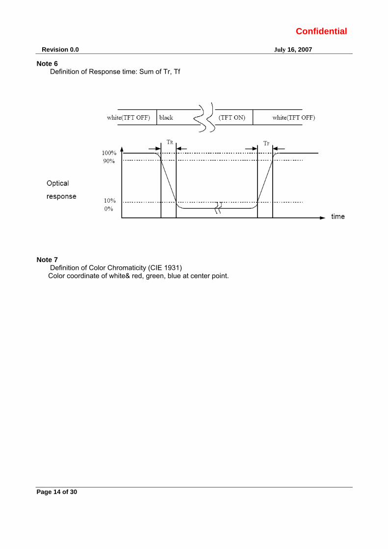
Note 6 Definition of Response time: Sum of Tr, Tf
Note 7
Definition of Color Chromaticity (CIE 1931) Color coordinate of white& red, green, blue at center point.

Revision 0.0 July 16, 2007
Page 15 of 30
Confidential
5. QUALIFICATION 5.1 Inspection condition. ① Temperature • Humidity
- Room Temperature : 23±3°C - Humidity : 60±20%
② Inspection distance and degree - Keep distance over 30cm from LCD surface under the 20W lighting source from the
lamp.
Inspects from Z to X and Y within Φ(Φ=30°)
The distance should be kept over 30cm.
- LCD surface and light source has to be perpendicular and inspection should be done
within 30° from the inspection position (Z-axis) .
Display surface Light source and LCD surface must
be aligned perpendicular.

Revision 0.0 July 16, 2007
Page 16 of 30
Confidential
5.2 Inspection method (Sampling) - General inspection.
1) Fail 1 (Heavy defect) : Unable to use product, cannot use product up to it’s expectation
and can not perform the standard of it’s purpose. 2) Fail 2 (Light defect) : Unstable and degraded product but still can be use. 3) Defect applied area : Active Area 4) Criterion : AQL of Fail 1 : 0.65, AQL of Fail 2 : 1.5
5.3 Inspection category - Sampling procedures for each item’s acceptance level
Defect type Sampling procedures AQL
Major defect MIL-STD-105D Inspection level Ⅰ
normal inspection
single sample inspection 0.65
Minor defect MIL-STD-105D Inspection level Ⅰ
normal inspection
single sample inspection 1.5
- Definition of Black / Spot or Line
Item Criterion for defects
Black / White spots (Ⅰ)
Black / White lines (Ⅰ)
Spots or lines appear dark or white in display patterns and remain unvaried in terms of size or shade with varying the LCD operating voltage.
Black / White spots (Ⅱ)
Black / White lines (Ⅱ)
Spots or lines appear dark or white in display patterns and they are variable in terms of size or shade with varying the LCD operating voltage.

Revision 0.0 July 16, 2007
Page 17 of 30
Confidential
5.4 Visual inspection
ITEM Criterion for defects Defect type
1) Non display • No non display is allowed Major
2) Irregular operation • No irregular operation is allowed Major
3) Short • No shorts are allowed Major
4) Open • Any segments or common patterns that don’t activate are rejectable. Major
5) Black / White spot (Ⅰ)
Size Ø (mm) Acceptable number
Ø ≤ 0.15 0.15 < Ø ≤ 0.20 0.20 < Ø ≤ 0.30
0.30 < Ø
Ignore 3 2 0
Minor
6) Black / White line (Ⅰ)
Length (mm) Width (mm) Acceptable number
10 < L 5.0 < L ≤ 10 10 < L ≤ 5.0
L ≤ 1.0
0.03 < W≤ 0.040.04 < W≤ 0.060.06 < W≤ 0.070.07< W≤ 0.09
5 3 2 1
Minor
7) Black / White spot (Ⅱ)
Size Ø (mm) Acceptable number
Ø ≤ 0.30 0.30 < Ø ≤ 0.50 0.50 < Ø ≤ 1.20
1.20 < Ø
Ignore 5 3 0
Minor
8) Black / White line (Ⅱ)
Length (mm) Width (mm) Acceptable number
20 < L 10 < L ≤ 20 5.0 < L ≤ 10
L ≤ 5.0
0.05 < W≤ 0.070.07 < W≤ 0.090.09 < W≤ 0.100.10< W≤ 0.15
5 3 2 1
Minor
9) Back Light
1) No Lighting is reject able 2) Flickering and abnormal lighting are rejectable ※ In case of the model with back light
(E/L, LED or CCFT type)

Revision 0.0 July 16, 2007
Page 18 of 30
Confidential
ITEM Criterion for defects Defect type
10) Display pattern
[Unit: mm]
Note : 1) Acceptable up to 3 damages
2) NG if there’re two or more pinholes per dot
A+B ≤ 0.30 2 0 < C D+E ≤ 0.25
2 F+G ≤ 0.25
2
Minor
11) Blemish & Foreign matters
Size: Ø=(A+B)/ 2
Size Ø (mm) Acceptable number
Ø ≤ 0.15 0.15 < Ø ≤ 0.20 0.20 < Ø ≤ 0.30
0.30 < Ø
Ignore 3 2 0
Minor
12) Scratch on Polarizer
Note (1) Regard as a blemish
Length (mm) Width (mm) Acceptable number Ignore L < 2.0 L > 2.0 L > 1.0 L ≤ 1.0
Note (1)
W≤ 0.03 0.03 < W≤ 0.05
0.05 < W≤ 0.08
0.08< W
Ignore Ignore
1 1
Ignore Note (1)
Minor
13) Bubble in Polarizer
Size Ø (mm) Acceptable number
Ø ≤ 0.20 0.20 < Ø ≤ 0.50 0.50 < Ø ≤ 0.80
0.80 < Ø
Ignore 3 2 0
Minor
14) Stains on LCD panel surface
Stains which cannot be removed even when wiped lightly with a soft cloth or similar cleaning too are rejectable. Minor
A
B

Revision 0.0 July 16, 2007
Page 19 of 30
Confidential
ITEM Criterion for defects Defect type
15) Rust in Bezel Rust which is visible in the bezel is rejectable. Minor
16) Defect of land surface contact (Poor soldering)
Evident crevices which is visible are rejectable. Minor
17) Parts mounting (1) Failure to mount parts (2) Parts not in the specifications are mounted (3) Polarity, for example, is reversed
Major Major Major
18) Parts alignment (1) LSI, IC lead width is more than 50% beyond pad outline. (2) Chip component is off center and more
Minor Minor
19) Conductive foreign matter(Solder ball, solder chips)
(1) 0.45 < Ø , N ≥ 1 (2) 0.30 < Ø ≤ 0.45 , N ≥ 1 Ø: Average diameter of solder ball (unit: mm) (3) 0.50 < L , N ≥ 1 L: Average length of solder chip (unit: mm)
Major Minor
Minor

Revision 0.0 July 16, 2007
Page 20 of 30
Confidential
5.5 Electrical inspection
[ L : length, N : count ] Inspection pattern for electrical defect should be pure R,G,B Black and White. Light leakage not allowed Image sticking image sticking pattern shall not be to persist longer than 10 seconds in
the next pattern Glue / stain / dirt glue, non-removable stain and dirt which are visible in the inspection area
are not acceptable.
Defect Type Accept Reject
Bright dot (Fig 1)
Random
Two adjacent
N <= 7 N > 7
N <= 3 N > 3
Dark dot (Fig 2) Random Two adjacent Three adjacent Four or more adjacent
N <= 7 N <= 4 N <= 2
N > 7 N > 4 N > 2
Not allowed
Maximum allowable number of dot defect N <= 14 N > 14
Minimum distance between defects (Fig 3) bright dot – to – bright dot dark dot – to – dark dot bright dot – to – dark dot
L => 4mm Don’t’ care Don’t’ care
L => 4mm Don’t’ care Don’t’ care
Revision 0.0 July 16, 2007
Page 21 of 30
Confidential
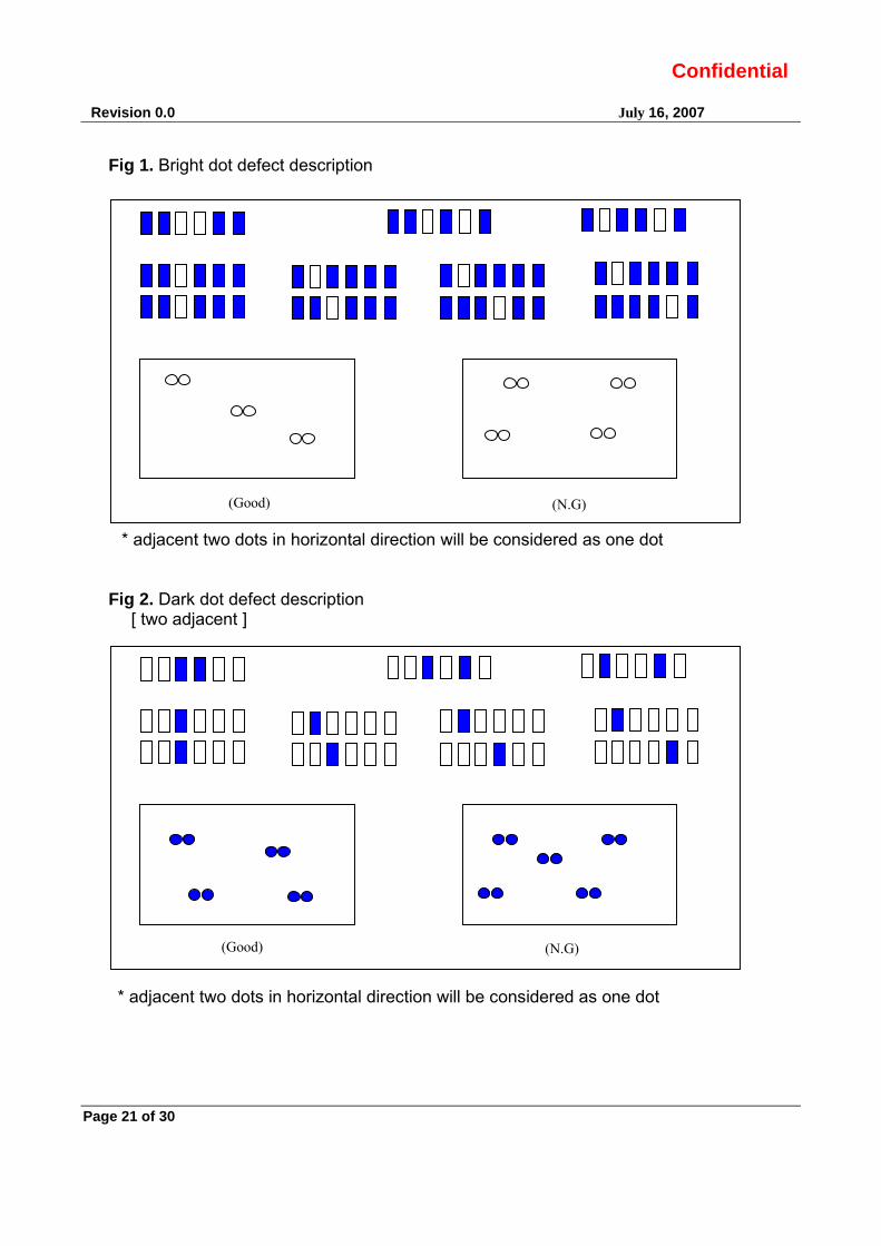
Fig 1. Bright dot defect description
* adjacent two dots in horizontal direction will be considered as one dot
Fig 2. Dark dot defect description [ two adjacent ]
* adjacent two dots in horizontal direction will be considered as one dot
(Good) (N.G)
(Good) (N.G)

Revision 0.0 July 16, 2007
Page 22 of 30
Confidential
Fig 2. Dark dot defect description – continued [ three adjacent ]
Fig 3. Minimum distance between dot defects [ Bright dot - to - Bright ]
(Good) (N.G)
(Good) (N.G)
4mm 3.9mm
Revision 0.0 July 16, 2007
Page 23 of 30
Confidential
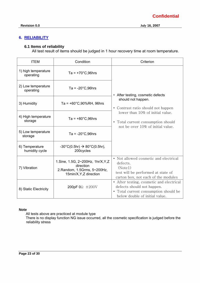
6. RELIABILITY 6.1 Items of reliability All test result of items should be judged in 1 hour recovery time at room temperature.
ITEM Condition Criterion
1) high temperature operating Ta = +70°C,96hrs
• After testing, cosmetic defects should not happen.
• Contrast ratio should not happen
lower than 10% of initial value.
• Total current consumption should
not be over 10% of initial value.
2) Low temperature operating Ta = -20°C,96hrs
3) Humidity Ta = +60°C,90%RH, 96hrs
4) High temperature storage Ta = +80°C,96hrs
5) Low temperature storage Ta = -20°C,96hrs
6) Temperature humidity cycle
-30°C(0.5hr) 80°C(0.5hr), 200cycles
7) Vibration
1.Sine, 1.5G, 2~200Hz, 1hr/X,Y,Z direction
2.Random, 1.5Grms, 5~200Hz, 15min/X,Y,Z direction
• Not allowed cosmetic and electrical
defects.
(Note1)
test will be performed at state of
carton box, not each of the modules
8) Static Electricity 200pF 0Ω ±200V
• After testing, cosmetic and electrical
defects should not happen.
• Total current consumption should be
below double of initial value. Note All tests above are practiced at module type There is no display function NG issue occurred, all the cosmetic specification is judged before the
reliability stress

Revision 0.0 July 16, 2007
Page 24 of 30
Confidential
7. HANDLING 7.1 Handling
- LCD module is composed of the fragile glass attached weak polarizer film. Thus it can be damaged easily. Everyone needs to handle very carefully without shock by dropping and damage or dust on the surface.
7.2 Handling and cleaning of LCD - While cleaning LCD module (see below) take soft cloth and wipe it carefully with
cleaning solvent. ◎ Isopropyl alcohol ◎ Ethyl alcohol ◎ Trichloroethylene
- To prevent damage to module, do not wipe with hard fabric. Do not use below cleaning solvent. ◎ Water ◎ Ketone ◎ Aromatics
- To prevent damage to ITO pad ◎ HCFC ◎ Soldering flux
◎ CI, S ◎ Spittle, Fingerprint
- Products include pad to prevent corrosion to ITO. Hahotech recommend that all products include pad to it’s products. If customer damages ITO using chemicals or solvent not recommend by manufacture, than customer is liable and responsible for the damages caves to product.
7.3 Electrostatic Shielding - LCD modules uses C-MOS LSI driver, so we recommend our customer as so;
Do not press key or send signals before power on. In order to prevent additional electrostatic damage, should do earth any operator and tools for the product manufacturing. When removing the protective film from LCD, electrostatic damage happens. Therefore we are continuously testing to countermeasure against electrostatic damage and making sure the shielding method for the product safety.
7.4 Packing
- It is standard to keep LCD modules in package. Please note below when keeping out of package. - LCD modules are composed of glass, so be careful not to put pressure, impact or drop it in anyway. - To prevent damages do not place it in high temperature/humidity, Also when safe keeping do not directly place in sun.

Revision 0.0 July 16, 2007
Page 25 of 30
Confidential
7.5 Layout and How to use - In case not following normal POWER ON, OFF order, can nausea damages that are not
recoverable. Also not following normal procedures can cause permanent damages.
- Using under below the normal operating temperature the response time can be delayed and using under higher operating temperature the color can show darker than normal. But these conditions do not mean the LCD is a defect. It will recover back to normal, once using it in a normal operating temperature. - Color of LCD can change if put to a pressure, and will not operate normal. So, the layout must show that LCD modules can be protected with think layer of protection under pressure.
- Do not force or pull the LCD module connector or cables. TAIL draws a plan not to become TOUCH at the region which the transit does FOLDER HINGE.
- VDD of LCD MODULE POWER LINE must draw a plan in SET WINDOW. - Needs to be design up to the EMI standards. - The design must do SET WINDOW so that it is suitable to VIEWING AREA. - The mark characteristic except VIEWING AREA can not guarantee.
7.6 Safekeeping - Do not place under direct fluorescent light or beam of light. - Do not place near water or where water can reach, can cause erosion and rust. - We do at a polarizer surface lest the store it should be touched you being due to at
anything. The encouragement does with the outgoing putting at an inside courage to keep.
7.7 Safety - Do not open module, can cause damages from sharp objects. - In case of breaking the LCD, a liquid can leak from it. If come in contact with liquid, wash off with water immediately. - Do not touch LCD module with bare hands, can cause static electricity.
Revision 0.0 July 16, 2007
Page 26 of 30
Confidential
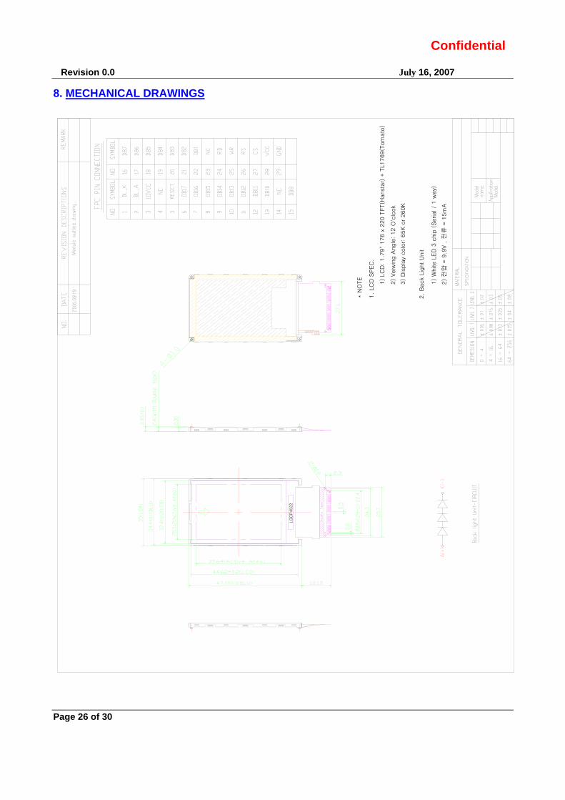
8. MECHANICAL DRAWINGS
1)
White L
ED
3 c
hip
(Serial /
1 w
ay)
1)
LC
D:
1.7
9"
176 x
220 T
FT(H
anst
ar)
+ T
L1769(T
om
ato
)
2)
전압
= 9
.9V ,
전류
= 1
5m
A
3)
Dis
pla
y colo
r: 6
5K o
r 260K
2)
Veiw
ing A
ngle
: 12 O
'clc
ok
2.
Back
Lig
ht U
nit
LG
DP4522
* N
OTE
1.
LC
D S
PEC
.
Revision 0.0 July 16, 2007
Page 27 of 30
Confidential
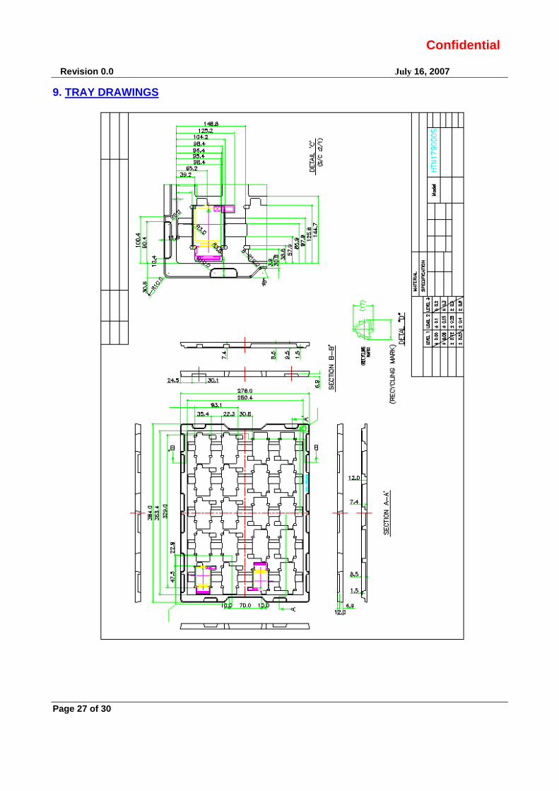
9. TRAY DRAWINGS
MyHome
텍스트 상자

Revision 0.0 July 16, 2007
Page 28 of 30
Confidential
10. BOX DRAWINGS
160 E
A /
Box-
Inner
41 2 3 2 1
PP T
ray
: 8 E
A
20 E
A / PP Tray
5 6
Box-
inner
: 4 E
A
384*2
78*1
2
59.2
3*3
5*2
.85
384*2
78*1
2
388*2
82*9
2
430*3
10*4
30
385*2
80*5
Dim
ensi
on
Cush
ion-S
ponge
NO
.
1
ITEM
CO
DE
-
Dum
my
Pla
stic
-Tra
y
Box-
Cart
on
Box-
Inner
Pla
stic
-Tra
y
LCD
Module
432 5 6
HTN1
7900
0S
HTN1
7900
0S
HTN1
7900
0S
- -
PE S
hee
t
Rem
ark
2EA
Q'n
ty
PP T
ray
Cap
1EA
640EA
1EA
4EA
32EA
PP T
ray
Tota
l Solu
tion
For
Flat
Panel D
isplq
y Busi
nes
s
■
()

Revision 0.0 July 16, 2007
Page 29 of 30
Confidential
11. FPC Circuit

Revision 0.0 July 16, 2007
Page 30 of 30
Confidential
12. Part list
MyHome
텍스트 상자