S. Pulipati, V. Ariyarathna, U. D. Silva, N. Akram, E ...
5
S. Pulipati, V. Ariyarathna, U. D. Silva, N. Akram, E. Alwan, A. Madanayake, S. Mandal, and T. S. Rappaport, “A Direct- Conversion Digital Beamforming Array Receiver with 800 MHz Channel Bandwidth at 28 GHz using Xilinx RF SoC,” 2019 IEEE International Conference on Microwaves, Communication, Antennas and Electronic Systems (COMCAS), Tel Aviv, Israel, Nov 2019, pp. 1-5. A Direct-Conversion Digital Beamforming Array Receiver with 800 MHz Channel Bandwidth at 28 GHz using Xilinx RF SoC Sravan Pulipati, Viduneth Ariyarathna, Udara De Silva, Najath Akram, Elias Alwan, Arjuna Madanayake Dept. of Elec. and Comp. Engineering Florida International University Miami, FL, USA amadanay@fiu.edu Soumyajit Mandal Dept. of Elec. Eng. and Comp. Science Case Western Reserve University Cleveland, OH, USA [email protected] Theodore S. Rappaport Dept. of Elec. and Comp. Engineering New York University New York,NY, USA [email protected] Abstract—This paper discusses early results associated with a fully-digital direct-conversion array receiver at 28 GHz. The proposed receiver makes use of commercial off-the-shelf (COTS) electronics, including the receiver chain. The design consists of a custom 28 GHz patch antenna sub-array providing gain in the elevation plane, with azimuthal plane beamforming provided by real-time digital signal processing (DSP) algorithms running on a Xilinx Radio Frequency System on Chip (RF SoC). The proposed array receiver employs element-wise fully-digital array processing that supports ADC sample rates up to 2 GS/second and up to 1 GHz of operating bandwidth per antenna. The RF mixed-signal data conversion circuits and DSP algorithms operate on a single-chip RF SoC solution installed on the Xilinx ZCU1275 prototyping platform. Index Terms—5G, MIMO, Multibeams, Beamforming, mm- wave I. I NTRODUCTION It is an exciting time for wireless communications. The rush to move to 5G in the 24/28 GHz bands (and eventually the 39 GHz band as well) has resulted in fierce competition among network providers and original equipment manufac- turers (OEM) to provide highly-adaptable, high-performance hardware and circuit solutions that take full advantage of the mm-wave spectrum. There are massive opportunities for new applications in the mm-wave space waiting to be ex- ploited, and new networks having high throughput, capacity and low latency are the starting point for the next wave of ‘Ubers, Facebooks, and Instagrams of the future’ [1], [2]. The networks of the future, at 28 GHz and beyond, will be based on electronic systems that heavily depend on the integration of radio-frequency (RF) electronics with digital back-ends that run software-defined radio (SDR) algorithms. Proposed sixth-generation (6G) networks will likely include a significant amount of artificial intelligence (AI) and RF machine learning (RF-MLS) algorithms. Regardless of the software approach, whether linear time invariant (LTI) or non- linear/ML/AI based, the ultimate performance of the network is still grounded on the performance of the analog front-ends array Phased array Phased - Blockage array Phased Blockage MIMO BEAMS (b) (a) Path length Path length l 2 e -jφ l 1 e -jφ e -jω l 1 c .e -jφ = e -jω l 2 c l 2 l 1 Fig. 1. Possible applications of MIMO + multi-beam beamforming (a) in a blocked LOS path; (b) to improve SNR when LOS is available by using multi-path techniques, and to connect across corners in an urban environment. that interface the information-carrying signals to the physical world. Components such as antennas, low-noise amplifiers (LNAs), and power amplifiers (PAs) for example, will continue to play an important role in emerging 5G/6G systems. The design of the mm-wave RF front-end is critically important because any loss of front-end performance is difficult, if not impossible, to correct in the digital post-processing back-end. Next-generation (6G) wireless access points will employ a combination of multi-input-multi-output (MIMO) theory with multi-beam fully-digital beamforming. The high-gain array factors provided by very sharp beams will be required for overcoming high path losses and also mitigating environment attenuation due to absorbing gases (e.g., oxygen at 60 GHz), rain, hail, dust, and other opaque objects (trees, humans) that degrade signal-to-noise ratio (SNR) at the receiver. Future networks will thus exploit both the massive bandwidth avail- able in the mm-wave bands, and also the high SNR available due to the use of high-gain antenna arrays to achieve spec- tral efficiency via orthogonal frequency division multiplexing (OFDM). In particular, the high SNR that can be achieved with digital beamforming will allow quadrature amplitude modulation (QAM) with up to 1024 discrete constellation points per OFDM sub-carrier. In addition, the combination of MIMO techniques with fully-digital multi-beam beamforming arXiv:1911.09180v1 [eess.SP] 20 Nov 2019
Transcript of S. Pulipati, V. Ariyarathna, U. D. Silva, N. Akram, E ...

S. Pulipati, V. Ariyarathna, U. D. Silva, N. Akram, E. Alwan, A. Madanayake, S. Mandal, and T. S. Rappaport, “A Direct- Conversion Digital BeamformingArray Receiver with 800 MHz Channel Bandwidth at 28 GHz using Xilinx RF SoC,” 2019 IEEE International Conference on Microwaves, Communication,
Antennas and Electronic Systems (COMCAS), Tel Aviv, Israel, Nov 2019, pp. 1-5.
A Direct-Conversion Digital Beamforming ArrayReceiver with 800 MHz Channel Bandwidth at 28
GHz using Xilinx RF SoCSravan Pulipati, Viduneth Ariyarathna,
Udara De Silva, Najath Akram,Elias Alwan, Arjuna Madanayake
Dept. of Elec. and Comp. EngineeringFlorida International University
Miami, FL, [email protected]
Soumyajit MandalDept. of Elec. Eng. and Comp. Science
Case Western Reserve UniversityCleveland, OH, USA
Theodore S. RappaportDept. of Elec. and Comp. Engineering
New York UniversityNew York,NY, USA
Abstract—This paper discusses early results associated witha fully-digital direct-conversion array receiver at 28 GHz. Theproposed receiver makes use of commercial off-the-shelf (COTS)electronics, including the receiver chain. The design consists ofa custom 28 GHz patch antenna sub-array providing gain inthe elevation plane, with azimuthal plane beamforming providedby real-time digital signal processing (DSP) algorithms runningon a Xilinx Radio Frequency System on Chip (RF SoC). Theproposed array receiver employs element-wise fully-digital arrayprocessing that supports ADC sample rates up to 2 GS/secondand up to 1 GHz of operating bandwidth per antenna. The RFmixed-signal data conversion circuits and DSP algorithms operateon a single-chip RF SoC solution installed on the Xilinx ZCU1275prototyping platform.
Index Terms—5G, MIMO, Multibeams, Beamforming, mm-wave
I. INTRODUCTION
It is an exciting time for wireless communications. Therush to move to 5G in the 24/28 GHz bands (and eventuallythe 39 GHz band as well) has resulted in fierce competitionamong network providers and original equipment manufac-turers (OEM) to provide highly-adaptable, high-performancehardware and circuit solutions that take full advantage ofthe mm-wave spectrum. There are massive opportunities fornew applications in the mm-wave space waiting to be ex-ploited, and new networks having high throughput, capacityand low latency are the starting point for the next wave of‘Ubers, Facebooks, and Instagrams of the future’ [1], [2].The networks of the future, at 28 GHz and beyond, willbe based on electronic systems that heavily depend on theintegration of radio-frequency (RF) electronics with digitalback-ends that run software-defined radio (SDR) algorithms.Proposed sixth-generation (6G) networks will likely includea significant amount of artificial intelligence (AI) and RFmachine learning (RF-MLS) algorithms. Regardless of thesoftware approach, whether linear time invariant (LTI) or non-linear/ML/AI based, the ultimate performance of the networkis still grounded on the performance of the analog front-ends
arrayP
hased
arrayP
hased
− Blockage
arrayP
hased
Blockage
MIMO BEAMS(b)(a)
Path length
Path lengthl2
e−jφ
l1
e−jφ
e−jω l1
c .e−jφ = e−jω l2
c
l2 l1
Fig. 1. Possible applications of MIMO + multi-beam beamforming (a) ina blocked LOS path; (b) to improve SNR when LOS is available by usingmulti-path techniques, and to connect across corners in an urban environment.
that interface the information-carrying signals to the physicalworld. Components such as antennas, low-noise amplifiers(LNAs), and power amplifiers (PAs) for example, will continueto play an important role in emerging 5G/6G systems. Thedesign of the mm-wave RF front-end is critically importantbecause any loss of front-end performance is difficult, if notimpossible, to correct in the digital post-processing back-end.
Next-generation (6G) wireless access points will employ acombination of multi-input-multi-output (MIMO) theory withmulti-beam fully-digital beamforming. The high-gain arrayfactors provided by very sharp beams will be required forovercoming high path losses and also mitigating environmentattenuation due to absorbing gases (e.g., oxygen at 60 GHz),rain, hail, dust, and other opaque objects (trees, humans) thatdegrade signal-to-noise ratio (SNR) at the receiver. Futurenetworks will thus exploit both the massive bandwidth avail-able in the mm-wave bands, and also the high SNR availabledue to the use of high-gain antenna arrays to achieve spec-tral efficiency via orthogonal frequency division multiplexing(OFDM). In particular, the high SNR that can be achievedwith digital beamforming will allow quadrature amplitudemodulation (QAM) with up to 1024 discrete constellationpoints per OFDM sub-carrier. In addition, the combination ofMIMO techniques with fully-digital multi-beam beamforming
arX
iv:1
911.
0918
0v1
[ee
ss.S
P] 2
0 N
ov 2
019

allows coherent combination of several ray-like channels (fromthe sharp beams) to achieve several important capabilities,such as 1) connecting when line-of-sight (LOS) is not availabledue to channel blockage, 2) connecting across corners ina densely built environment (e.g., downtown Miami/NYC),and 3) coherent combination of multiple ray-like channels toimprove SNR even when LOS is available. These scenariosare illustrated in Fig. 1 [3].
RX
RX
Phas
ed−
arra
y32−
elem
ents
Phas
ed−
arra
y32−
elem
ents
Phas
ed−
arra
y32−
elem
ents
TX
Phased
−array
32−
elemen
ts
Rx
RX
Rx
beam 1Rx
1
15
16 16
15
1
(FPGA CORE)
beam 16
TX
TX
Phased
−array
32−
elemen
tsP
hased
−array
32−
elemen
ts
ZynQ
Xilinx
RF−SoC
VCU−1275
beam 16
beam 15
beam 1Tx
Tx
Tx
beam 15
AD
C
DA
C
AD
C
DA
C
AD
C
DA
C
Fig. 2. System overview: a 16×16 beamforming+MIMO access point for 28GHz OFDM.
In this paper, we discuss the implementation of a four-element uniform linear array (ULA) in receive mode. Eachantenna element of this array operates at a center frequencyof 28 GHz and provides a bandwidth of about 800 MHz. Tothe authors’ knowledge, this is the first practically realized andexperimentally verified antenna array in this frequency rangethat provides such high bandwidth. The paper provides fulldesign schematics of the 28 GHz receiver, example antennadesigns, and details of the Xilinx RF SoC-based DSP back-endused for real-time signal processing at the physical layer.
II. DESIGN SPECIFICATIONS AND CONSTRAINTS
This section discusses the technical specifications of thereceiver, which is designed to support 64-QAM modulationfor 5G OFDM-based wireless communications. A descriptionof the design procedure can be found in [4].
The proposed receiver design is designed to operate in the27.5 GHz-28.35 GHz frequency range, which has been allo-cated for commercial 5G applications in the United States [5].The OFDM parameters listed below were used for the theo-retical calculations as well as to model the system using AWRMicrowave Office mm-wave (mmW) circuits and systemssimulator software: FFT size (NFFT ): 512, modulation (M ):64 QAM, guard interval (GI): 1/8, data subcarriers (ND):336, and subcarrier spacing (CS): 1.65 MHz. These systemparameters provide the required bandwidth (800 MHz) and amaximum data rate of
Rb =log2(M)×ND × CS
1 + GI=
6× 336× 1.65× 106
1 + 0.125' 3 Gbps. (1)
To establish a wireless communication link with bit errorrate (BER) better than 10−5 for M = 64, Eb/N0 should be at
I
Q
LOLNA IQ
Downconverter
LPF IFAmp
VGA
ADC
RF-SO
C
RXADC
Fig. 3. Architecture of the proposed mmW receiver.
least 17.8 dB [6]. Hence, the required SNR at the demodulatorinputs is given by
SNRdB =
(Eb
N0
)+ 10 log10
(log2(M)ND
(1 + GI)NFFT
)= 23.2 dB.
The receiver chain is designed by taking this SNR value as adesign constraint.
III. FRONT-END DESIGN
A system overview of the mmW front-end design is shownin Fig. 2 [3]. Note that our current implementation only uses 4elements. However, we plan to scale the system to 32 elementsin the near future.
A. Cascaded Noise Figure and Gain
The performance of the mm-wave receiver is optimizedto have a low noise figure (NF) and high gain. The firstLNA, which is directly connected to the antenna, largelysets the overall sensitivity and NF of the receiver. Thus itshould have the lowest NF in the chain. The best trade-offbetween the NF and gain of the LNA can be calculated usingwell-known microwave receiver design methods available inthe literature [7], [8]. A complete analysis of the maximumpossible noise figure Fcas and minimum possible gain Gcas forthe receiver chain to satisfy SNR= 23.2 dB is described in [3].The calculations were made under the assumptions that 1) thesignal levels at the input of the antenna are in the range of−85 dBm, and 2) each antenna of a 32 element array providesan individual gain of 15 dB. The reported noise figure and gainvalue requirements are 5.8 dB and 55 dB respectively.
B. Architecture and Component Selection
The proposed mmW receiver chain employs a superhetero-dyne IQ receiver architecture as shown in Fig. 3. The narrow-band nature of patch antennas eliminated the need for sep-arate band-pass filters. A low-side LO is used at the IQ-downconverter (HMC1065LP4E) to generate an intermediatefrequency (IF) signal of 0.15-1 GHz, which is further amplifiedand sampled by high speed RF-SoC ADCs. Careful selectionof components is critical for providing the desired NF andgain values. Components with higher third-order intercept(TOI) levels are desirable to provide better linearity and thushigher dynamic range (DR). The final component selectionsare shown in Table I.
Ideal values of cascaded gain and NF using the selectedcomponents are computed using standard formulas [7], result-ing in Gcas,dB = 70 dB and Fcas,dB = 2.5 dB. For the

TABLE ICOMPONENTS AND SPECIFICATIONS FOR THE MMW RECEIVER
Component Gain NF OIP3(dB) (dB) (dBm)
LNA (MAAL-01111) 19 2.5 20
Down converter (HMC1065LP4E) 9 3 14
Low-pass filter (LPF) (LFCN-900+) −1 1 N/A
IF amplifier (RAM-8A+) [31.5,24] 2.6 24.4
VGA (ADL5331) [−15,15] 9 39
gain calculation, we considered 1) the maximum gain of thevariable gain amplifier (VGA), and 2) the mid-band gain of theIF amplifier . The receiver’s noise performance is well withinthe NF requirements, and with the help of VGA (ADL5331)it also provides 30 dB of adjustable gain to increase DR, i.e.,keep the amplified signal levels within the full-scale range ofthe ADCs. Next, we evaluate and verify the performance ofthe proposed mmW receiver.
IV. PERFORMANCE EVALUATION
To evaluate the real-world performance of the selectedcomponents, a simulation test-bench was set up in AWRMicrowave Office simulation software. A 64 QAM OFDMmodulation scheme is employed, and the system is excitedusing only one OFDM subcarrier as the others were undergo-ing phase rotation. Correcting for this effect requires carefulcalibration, which will be undertaken in future work. Sinceonly one OFDM subcarrier is considered, applying ND = 1in (1) and recomputing, the detectable signal Pin at the antennawould be lowered to −110 dBm.
-4 -2 0 2 4
Constellation_OUT
-4
-2
0
2
4
IQ(TP.Constellation_Rx,250,1,1,0,0,0)OFDM System
IQ(TP.Constellation_TX,250,1,1,0,0,0)OFDM System
Fig. 4. Simulated constellation for a 64 QAM single sub-carrier at the receiverside for an input level of −110 dBm. Red and blue circles indicate the idealand measured values, respectively.
The AWR model is simulated with a receiver powerof −110 dBm at its input. At the center frequency ofthe IF band (fRf − fLO = 0.6 GHz), the values ofFcas, Gcas and OIP3cas were found to be 4.7 dB, 49.4 dB,and 35.6 dBm respectively. Fig. 4 compares the constellationsimulated after the QAM demodulator with an ideal 64-QAMconstellation. No appreciable difference was observed betweenthe ideal and simulated constellations. A numerical assessment
TABLE IISPECIFICATIONS FOR THE PATCH ANTENNA DESIGN
Frequency (f0) 28 GHzSubstrate RO4350B
Dielectric constant (εr) 3.66Dielectric height (h) 0.254 mm
TABLE IIIDIMENSIONS FOR THE PATCH ANTENNA DESIGN
Patches 1st, 8th 2nd, 7th 3rd, 6th 4th, 5thWidth 1.55 2.06 2.59 3.12Length 2.81 2.77 2.74 2.72
is being conducted to quantify how closely the behavior of thereal-world components matches those used in an ideal receiver.
V. 28 GHZ RECEIVER ARRAY SETUP
We use a custom 8-element series fed sub-array that em-ploys a series-feeding structure to decrease the width of thefield patterns in the vertical plane (elevation) so as to sup-press interference and spurious signals, thus providing moredirective gain. Additionally, designing a series-fed array withtapering of the patch widths helps in significantly reducingthe side lobe levels (SLLs) of the field patterns along theaxis of the array. In series-feeding, elements are spaced aguided wavelength apart along a uniform transmission line.By tapering the widths from one edge to center element inascending order, excitation is maximum at the center anddecreases as one approaches the edge, which results in a slightincrease in beam-width and reduction of gain when comparedto uniform excitation. The 28 GHz 8-element array is designedwith a linear tapering having −6 dB pedestal (to controlthe SLL). The patch array is analyzed using a transmissionline model [9] in conjunction with wavelength-apart series-fed analysis [10], to compute the dimensions of each patchthat produce the corresponding amplitude excitation.
Following the analysis described above, design dimensionsfor each patch were calculated for the board specificationsshown in Table II. The materials were chosen to optimizeperformance at mm-wave frequencies, and also to accountfor practical element and transmission line dimensions atthese frequencies. The sub-array is designed in CST antennasimulation software. The optimized dimensions for each patchare shown in Table III, and its geometry is shown in Fig. 5(a). Matching to the 50 Ω feed is based on a quarter-wavetransformer. Simulated and measured results for |S11| areshown in Fig. 5 (b) and (c) respectively, whereas far-fieldpatterns (vertical plane) are shown in Fig. 5(d). The proposedantenna resonates at 28.05 GHz with a return loss of 27.41 dB.The tapered 28 GHz array results in a SLL less than −18 dB,compared to −13 dB for uniform excitation.
A. Antenna Array Design
Design of the 8-element series fed sub-array on CST wasfollowed by the realization with an RF front end. The entireRF receiver setup is shown in Fig. 6(a) and a close up ofthe fabricated antenna is shown in Fig. 6(b). The 4-elementULA is built using four sub arrays with a separation of 0.75

51.5
mm
7.10 mm
1
2
3
4
5
6
7
8
(b) (c) (d)(a)
λ4
Fig. 5. (a) Dimensions of the antenna sub-array; (b) CST-simulated return loss (S11); (c) Measured return loss (S11); and (d) CST-simulated polar patternof the sub-array at 28 GHz. Note that the polar pattern is along the axis of the array i.e., in the elevation plane.
XilinxZCU1275Platform
ReceiverArray Transmitter
14GHzOscillator RF
Front-end
Receiverantennaarray
(a)
(b) (c)
Fig. 6. (a) The receiver setup for measurements; (b) Close-up of the fabricatedantenna sub-array; and (c) The transmit-receive link.
wavelengths (8.0 mm at 28 GHz). Each sub array is fedwith a separate RF front-end as described in Fig. 3 using thecomponents selected in Table I. A central LO is divided using afour-way splitter and used as the LO for the individual mixers.The single-ended outputs of each front-end are converted todifferential pairs in order to drive the Xilinx RF SoC’s built-in ADCs. The conversion uses RF baluns built using Mini-circuits TC1-1-13M+ RF transformers [11], which have 1 dBinsertion loss for signals from 4.5-1000 MHz.
B. Digital Back-End
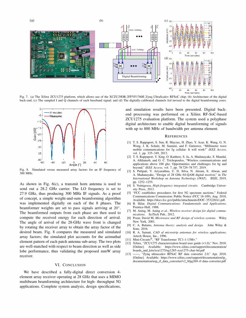
A Xilinx ZCU1275 evaluation board is used as the digitalprocessing back-end of the 28-GHz array receiver. The boardcontains a XCZU29DR-2FFVF1760E Zynq UltraScale+ RF-SoC chip, which integrates high-speed data converters alongwith a programmable logic fabric and application processingunit. Specifically, the chip supports 16 ADC channels upto 2GSPS and 16 DAC channels upto 4 GSPS. Fig. 7(a) shows a
close up of the Xilinx ZCU 1275 board, which provides BullsEye interfaces to access all the RFSoC’s data converters. AXilinx Analog Super Clock Module (HW-CLK-102) [12] thatsupports the ADC/DAC clock requirements is used to clock thedata converters. The 16 ADC inputs in the RFSoC are arrangedinto 4 tiles, each of which samples 4 channels. The HW-CLK-102 module supports four differential RF clocks for the ADCsand three phase-aligned reference clocks for synchronization.
The data converters were configured to sample at1966.08 MHz. To handle the total bandwidth of 800 MHz, thedigital circuits were designed in a polyphase architecture with8 parallel beamforming cores. Therefore, the built-in FIFOs ofthe Xilinx Data Converter IP (XDCIP) core were configuredto output a sample rate of 1966.08/8 = 245.76 MSps with 8sampled words per clock edge streamed into the beamformingcores. An overview of the digital back-end architecture isshown in Fig. 7(b). The outputs of each FIFO stream weresynchronized to a single reference clock of 245.76 MHz thatwas derived from the analog sampling clock. In this way, thedesign can use 8 parallel digital cores to process the entiresampled bandwidth, as shown in Fig. 7(b).
C. Calibration
The calibration mode of each ADC channel was set to“Mode-2” [13] in the XDCIP. In this mode, ADC calibration ishandled by the start-up finite-state-machine of the XDCIP. Inaddition, the RF front-ends were digitally calibrated using gainand phase correction. For this purpose, we added a complexmultiplier at each phase of each channel as shown in Fig. 7(b).The gain and phase mismatches with respect to a referencereceiver were pre-measured using a reference signal. Complexcalibration constants αi + jβi, where i = 0, 1, 2, 3 andα, β ∈ R, were then estimated for each channel. TypicalI and Q baseband channel data measured for a reference inputsignal before calibration are shown in Fig. 7(c). Fig. 7(c)shows the digitally-calibrated versions that are fed into thedigital beamforming cores.
D. Real-Time Beamforming and Measurement Setup
Fig. 6(a) shows the entire 28-GHz transmitter and receiverarray setup used for measuring beams in real-time beams.
FIF
O
FIF
O
FIF
O
FIF
O
(c)
(d)
(b)(a)
Digital Beamforming
I0
Q0
Q3
I3
1966.08MSps
245.76MSps
β0
α0β3
α3
Fig. 7. (a) The Xilinx ZCU1275 platform, which allows use of the XCZU29DR-2FFVF1760E Zynq UltraScale+ RFSoC chip; (b) Architecture of the digitalback-end; (c) The sampled I and Q channels of each baseband signal; and (d) The digitally-calibrated channels fed invised to the digital beamforming cores.
Fig. 8. Simulated versus measured array factors for an IF frequency of300 MHz.
As shown in Fig. 6(c), a transmit horn antenna is used tosend out a 28.2 GHz carrier. The LO frequency is set to27.9 GHz, thus producing 300 MHz IF signals. As a proofof concept, a simple weight-and-sum beamforming algorithmwas implemented digitally on each of the 8 phases. Thebeamformer weights are set to pass signals arriving at 20.The beamformed outputs from each phase are then used tocompute the received energy for each direction of arrival.The angle of arrival of the 28-GHz wave front is changedby rotating the receiver array to obtain the array factor of thedesired beam. Fig. 8 compares the measured and simulatedarray factors; the simulated plot accounts for the azimuthalelement pattern of each patch antenna sub-array. The two plotsare well-matched with respect to beam direction as well as sidelobe performance, thus validating the proposed mmW arrayreceiver.
VI. CONCLUSION
We have described a fully-digital direct conversion 4-element array receiver operating at 28 GHz that uses a MIMOmultibeam beamforming architecture for high- throughput 5Gapplications. Complete system analysis, design specifications,
and simulation results have been presented. Digital back-end processing was performed on a Xilinx RF-SoC-basedZCU1275 evaluation platform. The system used a polyphasedigital architecture to enable digital beamforming of signalswith up to 800 MHz of bandwidth per antenna element.
REFERENCES
[1] T. S. Rappaport, S. Sun, R. Mayzus, H. Zhao, Y. Azar, K. Wang, G. N.Wong, J. K. Schulz, M. Samimi, and F. Gutierrez, “Millimeter wavemobile communications for 5g cellular: It will work!” IEEE Access,vol. 1, pp. 335–349, 2013.
[2] T. S. Rappaport, Y. Xing, O. Kanhere, S. Ju, A. Madanayake, S. Mandal,A. Alkhateeb, and G. C. Trichopoulos, “Wireless communications andapplications above 100 ghz: Opportunities and challenges for 6g andbeyond,” IEEE Access, vol. 7, pp. 78 729–78 757, 2019.
[3] S. Pulipati, V. Ariyarathna, U. D. Silva, N. Akram, E. Alwan, andA. Madanayake, “Design of 28 GHz 64-QAM digital receiver,” in TheInternational Workshop on Antenna Technology (iWAT). IEEE, 2019,pp. 1252–1255.
[4] S. Voinigescu, High-frequency integrated circuits. Cambridge Univer-sity Press, 2013.
[5] “FCC establishes procedures for first 5G spectrum auctions,” FederalCommunications Commission: Public Notice (FCC 18-109), Aug. 2018,Available: https://docs.fcc.gov/public/attachments/DOC-353228A1.pdf.
[6] B. Sklar, Digital Communications: Fundamentals and Applications.Prentice-Hall, 1988.
[7] M. Aning, M. Aning et al., Wireless receiver design for digital commu-nications. SciTech Pub., 2012.
[8] Pozar, David M, Microwave and RF design of wireless systems. WileyNew York, 2001.
[9] C. A. Balanis, Antenna theory: analysis and design. John Wiley &Sons, 2016.
[10] R. A. Sainati, CAD of microstrip antennas for wireless applications.Artech House, Inc., 1996.
[11] Mini-Circuits®, “RF Transformer TC1-1-13M+.”[12] Xilinx, “ZCU1275 characterization board user guide (v1.0),” Nov. 2018.
[Online]. Available: https://www.xilinx.com/support/documentation/boards and kits/zcu1275/ug1285-zcu1275-char-bd.pdf
[13] ——, “Zynq ultrascale+ RFSoC RF data converter 2.0,” Apr. 2018.[Online]. Available: https://www.xilinx.com/support/documentation/ipdocumentation/usp rf data converter/v2 0/pg269-rf-data-converter.pdf