RX62N/RX621 Group Datasheet - RS...
146
R01DS0052EJ0110 Rev.1.10 Page 1 of 146 Feb 10, 2011 Datasheet RX62N/RX621 Group RENESAS 32-Bit MCU Features ■32-bit RX CPU Core Delivers 165 DMIPS at a maximum operating frequency of 100 MHz Single Precision 32-bit IEEE-754 Floating Point Accumulator: 32 × 32 to 64-bit result, one instruction Mult/Divide Unit, 32 × 32 Multiply in one CPU clock for multiple instructions Interrupt response in as few as 5 CPU clock cycles CISC-Harvard Architecture with 5-stage pipeline Variable length instructions, ultra compact code Supports the Memory Protection Unit (MPU) Background JTAG debug plus high-speed trace ■Low Power Design and Architecture 2.7V to 3.6V operation from a single supply 480 μA/MHz Run Mode with all peripherals on Deep Software Standby Mode with RTC Four low power modes ■Main Flash Memory, no Wait-State 100 MHz operation, 10 nsec read cycle No wait states for read at full CPU speed 256K, 384K, 512K Byte size options For Instructions or Operands Programming from USB, SCI, JTAG, user code ■Data Flash Memory Up to 32K Bytes with 30K Erase Cycles Background Erase/Program does not stall CPU ■SRAM, no Wait-State 64K or 96K Byte size options For Operands or Instructions Back-up retention in Deep Software Standby Mode ■DMA Four fully programmable internal DMA channels Two EXDMA channels for external-to-external transfers Data Transfer Controller (DTC) ■Reset and Supply Management Power-On Reset (POR) monitor/generator Low Voltage Detect (LVD) with precision setting ■System Clocking with Clock Monitoring External crystal, 8 MHz to 14 MHz to Internal PLL PLL source to system, USB, and Ethernet Internal 125 kHz LOCO for IWDT External crystal, 32 kHz for RTC ■Real Time Clock Full calendar function, BCD format ■Two Independent Watchdog Timers 125-kHz LOCO operation ■Up to 14 Communication Interfaces (2) USB 2.0 Full-Speed interfaces with PHY Supports Host/Function/OTG 10 endpoints for types: Control, Interrupt, Bulk, Isochronous (1) Ethernet MAC 10/100 Mbps, Half or Full Duplex Supported. Dedicated DMA with 2-Kbyte transmit and receive FIFOs. RMII or MII interface to external PHY (1) CAN ISO11898-1, supports 32 mailboxes (6) SCI channels: Asynchronous, clock sync, smartcard, and 9-bit modes (2) I 2 C interfaces up to 1M bps, SMBus support (2) RSPI ■External Address Space Eight CS areas (8 × 16 Mbytes) 128-Mbyte SDRAM area 8-/16-/32-bit bus space selectable for each area ■TFT-LCD up to WQVGA resolution ■Up to 20 Extended Function Timers (12) 16-bit MTU2 Input capture, Output Compare, PWM output, phase count mode (4) 8-bit TMR (4) 16-bit CMT ■1-MHz ADC units with two combination choices 12-bit × 8 ch. unit with single sample/hold circuit or (2) 10-bit × 4 ch units each with a sample/hold circuit AD-converted value addition mode (12-bit A/D converter) ■10-bit DAC, 2 channels ■Up to 128 GPIO 5V tolerant, Open-Drain, Internal Pull-up ■Operation Temp –40°C to +85°C TFLGA85 7×7mm, 0.65mm pitch TFLGA145 9×9mm, 0.65mm pitch LFBGA176 13×13mm, 0.8mm pitch LQFP100 14×14mm, 0.5mm pitch LQFP144 20×20mm, 0.5mm pitch 100 MHz 32-bit RX MCU with FPU, 165 DMIPS, up to 512-Kbyte Flash, Ethernet, USB 2.0 Full-Speed Host/Function/OTG, CAN, 12-bit ADC, TFT-LCD, RTC, up to 14 communication channels Features R01DS0052EJ0110 Rev.1.10 Feb 10, 2011
Transcript of RX62N/RX621 Group Datasheet - RS...

R01DS0052EJ0110 Rev.1.10 Page 1 of 146Feb 10, 2011
Datasheet
RX62N/RX621 GroupRENESAS 32-Bit MCU
Features32-bit RX CPU Core
Delivers 165 DMIPS at a maximum operating frequency of 100 MHz
Single Precision 32-bit IEEE-754 Floating Point Accumulator: 32 × 32 to 64-bit result, one instruction Mult/Divide Unit, 32 × 32 Multiply in one CPU clock for
multiple instructions Interrupt response in as few as 5 CPU clock cycles CISC-Harvard Architecture with 5-stage pipeline Variable length instructions, ultra compact code Supports the Memory Protection Unit (MPU) Background JTAG debug plus high-speed trace
Low Power Design and Architecture
2.7V to 3.6V operation from a single supply 480 µA/MHz Run Mode with all peripherals on Deep Software Standby Mode with RTC Four low power modes
Main Flash Memory, no Wait-State
100 MHz operation, 10 nsec read cycle No wait states for read at full CPU speed 256K, 384K, 512K Byte size options For Instructions or Operands Programming from USB, SCI, JTAG, user code
Data Flash Memory
Up to 32K Bytes with 30K Erase Cycles Background Erase/Program does not stall CPU
SRAM, no Wait-State
64K or 96K Byte size options For Operands or Instructions Back-up retention in Deep Software Standby Mode
DMA
Four fully programmable internal DMA channels Two EXDMA channels for external-to-external transfers Data Transfer Controller (DTC)
Reset and Supply Management
Power-On Reset (POR) monitor/generator Low Voltage Detect (LVD) with precision setting
System Clocking with Clock Monitoring
External crystal, 8 MHz to 14 MHz to Internal PLL PLL source to system, USB, and Ethernet Internal 125 kHz LOCO for IWDT External crystal, 32 kHz for RTC
Real Time Clock
Full calendar function, BCD format
Two Independent Watchdog Timers
125-kHz LOCO operation
Up to 14 Communication Interfaces
(2) USB 2.0 Full-Speed interfaces with PHY Supports Host/Function/OTG
10 endpoints for types: Control, Interrupt, Bulk, Isochronous (1) Ethernet MAC 10/100 Mbps, Half or Full Duplex
Supported.Dedicated DMA with 2-Kbyte transmit and receive FIFOs.RMII or MII interface to external PHY
(1) CAN ISO11898-1, supports 32 mailboxes (6) SCI channels: Asynchronous, clock sync, smartcard,
and 9-bit modes (2) I2C interfaces up to 1M bps, SMBus support (2) RSPI
External Address Space
Eight CS areas (8 × 16 Mbytes) 128-Mbyte SDRAM area 8-/16-/32-bit bus space selectable for each area
TFT-LCD up to WQVGA resolution
Up to 20 Extended Function Timers
(12) 16-bit MTU2Input capture, Output Compare, PWM output, phase count mode
(4) 8-bit TMR (4) 16-bit CMT
1-MHz ADC units with two combination choices
12-bit × 8 ch. unit with single sample/hold circuit or (2) 10-bit × 4 ch units each with a sample/hold circuit AD-converted value addition mode (12-bit A/D converter)
10-bit DAC, 2 channels
Up to 128 GPIO
5V tolerant, Open-Drain, Internal Pull-up
Operation Temp
–40°C to +85°C
TFLGA85 7×7mm, 0.65mm pitchTFLGA145 9×9mm, 0.65mm pitchLFBGA176 13×13mm, 0.8mm pitch
LQFP100 14×14mm, 0.5mm pitchLQFP144 20×20mm, 0.5mm pitch
100 MHz 32-bit RX MCU with FPU, 165 DMIPS, up to 512-Kbyte Flash, Ethernet, USB 2.0 Full-Speed Host/Function/OTG, CAN, 12-bit ADC, TFT-LCD, RTC, up to 14 communication channels
Features
R01DS0052EJ0110Rev.1.10
Feb 10, 2011

R01DS0052EJ0110 Rev.1.10 Page 2 of 146Feb 10, 2011
RX62N Group, RX621 Group 1. Overview
1. Overview
1.1 Outline of Specifications
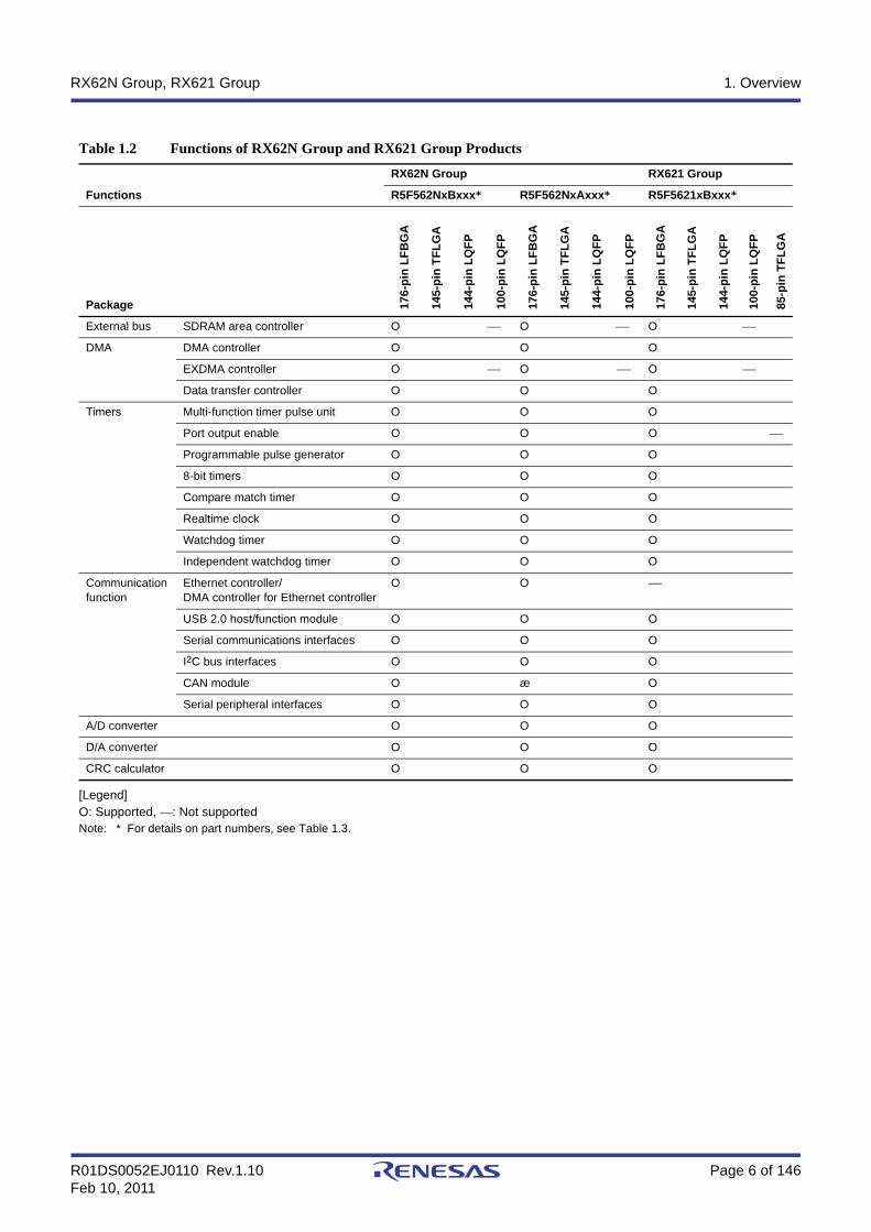
Table 1.1 lists the specifications in outline, and Table 1.2 lists the functions of products.
Table 1.1 Outline of Specifications (1 / 4)
Classification Module/Function Description
CPU CPU · Maximum operating frequency: 100 MHz· 32-bit RX CPU· Minimum instruction execution time: One instruction per state (cycle of the system clock)· Address space: 4-Gbyte linear· Register set of the CPU
General purpose: Sixteen 32-bit registersControl: Nine 32-bit registersAccumulator: One 64-bit register
· Basic instructions: 73· Floating-point instructions: 8· DSP instructions: 9· Addressing modes: 10· Data arrangement
Instructions: Little endianData: Selectable as little endian or big endian
· On-chip 32-bit multiplier: 32 x 32 64 bits· On-chip divider: 32 / 32 32 bits· Barrel shifter: 32 bits· Memory-protection unit (MPU) (as an optional function)*1
FPU · Single precision (32-bit) floating point· Data types and floating-point exceptions in conformance with the IEEE754 standard
Memory ROM · ROM capacity: 512 Kbytes (max.)· Two on-board programming modes
Boot mode (The user MAT is programmable via the SCI and USB.)User program mode
· Parallel programmer mode (for off-board programming)
RAM RAM capacity: 96 Kbytes (max.)
Data flash Data flash capacity: 32 Kbytes
MCU operating modes · Single-chip mode, on-chip ROM enabled expansion mode, and on-chip ROM disabled expansion mode (software switching)
Clock Clock generation circuit
· Two circuits: Main clock oscillator and subclock oscillator· Internal oscillator: Low-speed on-chip oscillator· Structure of a PLL frequency synthesizer and frequency divider for selectable operating
frequency· Oscillation stoppage detection· Independent frequency-division and multiplication settings for the system clock (ICLK),
peripheral module clock (PCLK), and external bus clock (BCLK)The CPU and other bus masters run in synchronization with the system clock (ICLK): 8 to 100 MHzPeripheral modules run in synchronization with the peripheral module clock (PCLK): 8 to 50 MHz
· Devices connected to the external bus run in synchronization with the external bus clock (BCLK): 8 to 50 MHz
Reset · Pin reset, power-on reset, voltage-monitoring reset, watchdog timer reset, independent watchdog timer reset, and deep software standby reset
Voltage detection circuit · When the voltage on VCC falls below the voltage detection level (Vdet), an internal reset or internal interrupt is generated.
Low power consumption
Low power consumption facilities
· Module stop function· Four low power consumption modes
Sleep mode, all-module clock stop mode, software standby mode, and deep software standby mode

R01DS0052EJ0110 Rev.1.10 Page 3 of 146Feb 10, 2011
RX62N Group, RX621 Group 1. Overview
Interrupt Interrupt control unit · Peripheral function interrupts: 146 sources· External interrupts: 16 (pins IRQ0 to IRQ15)· Non-maskable interrupts: 3 (the NMI pin, oscillation stop detection interrupt, and voltage-
monitoring interrupt)· Sixteen levels specifiable for the order of priority
User break controller (as an optional function)
· Two breakpoint channels· Address breaks in fetch cycles are specifiable (enabling ROM correction)
External bus extension · The external address space can be divided into nine areas (CS0 to CS7, SDCS), each with independent control of access settings.Capacity of each area: 16 Mbytes (CS0 to CS7), 128 Mbytes (SDCS)A chip-select signal (CS0# to CS7#, SDCS#) can be output for each area.Each area is specifiable as an 8-, 16-, or 32-bit bus space (however, only 176-pin versions support 32-bit bus spaces).The data arrangement in each area is selectable as little or big endian (only for data).
· SDRAM interface connectable· Bus format: Separate buses· Wait control· Write buffer facility
DMA DMA controller · 4 channels· Three transfer modes: Normal transfer, repeat transfer, and block transfer· Activation sources: Software trigger, external interrupts, and interrupt requests from
peripheral functions
EXDMA controller · 2 channels· Four transfer modes: Normal transfer, repeat transfer, block transfer, and cluster transfer· Single-address transfer enabled with the EDACK signal· Capable of direct data transfer to TFT LCD panels· Activation sources: Software trigger, external DMA requests (EDREQ), and interrupt
requests from peripheral functions
Data transfer controller
· Three transfer modes: Normal transfer, repeat transfer, and block transfer· Activation sources: Software trigger, external interrupts and interrupt requests from
peripheral functions
I/O ports Programmable I/O ports
· I/O ports for the 176-pin LFBGA/145-pin TFLGA/144-pin LQFP/100-pin LQFP/85-pin TFLGA
· I/O pins: 126/103/103/72/58· Input pins: 2/2/2/2/2· Pull-up resistors: 56/44/44/40/28· Open-drain outputs: 35/33/33/27/23· 5-V tolerance: 11/11/11/7/6
Timers Multi-function timer pulse unit
· (16 bits x 6 channels) x 2 units· Time bases for the 12 16-bit timer channels can be provided via up to 32 pulse-input/
output lines and six pulse-input lines· Select from among eight counter-input clock signals for each channel (PCLK/1, PCLK/4,
PCLK/16, PCLK/64, MTCLKA, MTCLKB, MTCLKC, MTCLKD) other than channel 5, for which only four signals are available.
· Input capture function· 21 output compare/input capture registers· Pulse output mode· Complementary PWM output mode· Reset synchronous PWM mode· Phase-counting mode· Generation of triggers for A/D converter conversion
Port output enable · Controls the high-impedance state of the MTU’s waveform output pins
Table 1.1 Outline of Specifications (2 / 4)
Classification Module/Function Description

R01DS0052EJ0110 Rev.1.10 Page 4 of 146Feb 10, 2011
RX62N Group, RX621 Group 1. Overview
Timers Programmable pulse generator
· (4 bits x 4 groups) x 2 units· Pulse output with the MTU output as a trigger· Maximum of 32-bit pulse output possible
8-bit timers · (8 bits x 2 channels) x 2 units· Select from among seven internal clock signals (PCLK, PCLK/2, PCLK/8, PCLK/32,
PCLK/64, PCLK/1024, PCLK/8192) and one external clock signal· Capable of output of pulse trains with desired duty cycles or of PWM signals· The 2 channels of each unit can be cascaded to create a 16-bit timer· Generation of triggers for A/D converter conversion· Capable of generating baud-rate clocks for SCI5 and SCI6
Compare match timer
· (16 bits x 2 channels) x 2 units· Select from among four internal clock signals (PCLK/8, PCLK/32, PCLK/128, PCLK/512)
Watchdog timer · 8 bits x 1 channel· Select from among eight counter-input clock signals (PCLK/4, PCLK/64, PCLK/128,
PCLK/512, PCLK/2048, PCLK/8192, PCLK/32768, PCLK/131072)· Switchable between watchdog timer mode and interval timer mode
Independent watchdog timer
· 14 bits x 1 channel· Counter-input clock: Dedicated on-chip oscillator
Realtime clock · Clock source: Subclock· Time/calendar
Interrupt sources: Alarm interrupt, periodic interrupt, and carry interrupt
Communicationfunction
Ethernet controller · Input and output of Ethernet/IEEE 802.3 frames· Transfer at 10 or 100 Mbps· Full- and half-duplex modes· MII (Media Independent Interface) or RMII (Reduced Media Independent Interface) as
defined in IEEE 802.3u· Detection of Magic PacketsTM* or output of a "wake-on-LAN" signal (WOL)· Compliance with flow control as defined in IEEE 802.3x standards
Note: * Magic PacketTM is a registered trademark of Advanced Micro Devices, Inc.
DMA controller for Ethernet controller
· Alleviation of CPU loads by the descriptor control method· Transmission FIFO: 2 Kbytes; Reception FIFO: 2 Kbytes
USB 2.0 host/function module
· Includes a UDC (USB Device Controller) and transceiver for USB 2.0· Single port (176-pin products: two ports)· Compliance with the USB 2.0 specification· Transfer rate: Full speed (12 Mbps)· Self-power mode and bus power are selectable· OTG (On the Go) operation is possible· Incorporates 2 Kbytes of RAM as a transfer buffer
Serial communications interfaces
· 6 channels· Serial communications modes:
Asynchronous, clock synchronous, and smart-card interface· Multi-processor communications function· On-chip baud rate generator allows selection of the desired bit rate· Choice of LSB-first or MSB-first transfer· Average transfer rate clock can be input from TMR timers for SCI5 and SCI6
Table 1.1 Outline of Specifications (3 / 4)
Classification Module/Function Description

R01DS0052EJ0110 Rev.1.10 Page 5 of 146Feb 10, 2011
RX62N Group, RX621 Group 1. Overview
Note 1. As for the MPU, contact your Renesas sales agency.Note 2. For products in the 100-pin LQFP and 85-pin TFLGA, BCLK is synchronized with 8 to 25 MHz.Note 3. MSB-first order is only available in the smart-card interface mode.
Communicationfunction
I2C bus interfaces · 2 channels (100-pin version: 1 channel)· Communications formats
I2C bus format/SMBus formatMaster/slave selectable (For multi-master operation)
CAN module · 1 channel· 32 mailboxes
Serial peripheral interfaces
· 2 channels· RSPI transfer facility
Using the MOSI (master out, slave in), MISO (master in, slave out), SSL (slave select), and RSPI clock (RSPCK) signals enables serial transfer through SPI operation (four lines) or clock-synchronous operation (three lines) Capable of handling serial transfer as a master or slave
· Data formatsSwitching between MSB first and LSB firstThe number of bits in each transfer can be changed to any number of bits from 8 to 16, or to 20, 24, or 32 bits.128-bit buffers for transmission and receptionUp to four frames can be transmitted or received in a single transfer operation (with each frame having up to 32 bits)
· Buffered structure· Double buffers for both transmission and reception
12-bit A/D converter10-bit A/D converter
· 12 bits x 1 unit (1 unit x 8 channels) or 10 bits x 2 units (2 units x 4 channels); 12- and 10-bit A/D converters can be exclusively used.
· 10- or 12-bit resolution· Conversion time: 1.0 s per channel (in operation with PCLK at 50 MHz)· Two operating modes
Single modeScan mode (one-cycle scan mode or continuous scan mode)
· Sample-and-hold function· Three ways to start A/D conversion
Conversion can be started by software, a conversion start trigger from a timer (MTU or TMR), or an external trigger signal.
· Self-diagnostic functions
D/A converter · 2 channels (1 channel for 100-pin products)· 10-bit resolution· Output voltage: 0 V to VREFH
CRC calculator · CRC code generation for arbitrary amounts of data in 8-bit units· Select any of three generating polynomials:
X8 + X2 + X + 1, X16 + X15 + X2 + 1, or X16 + X12 + X5 + 1.· Generation of CRC codes for use with LSB-first or MSB-first communications is
selectable.
Operating frequency 8 to 100 MHz
Power supply voltage VCC = PLLVCC = AVCC = 2.7 to 3.6V, VREFH = 2.7 to AVCC
Operating temperature 40 to +85C
Package 176-pin LFBGA (PLBG0176GA-A), 145-pin TFLGA (PTLG0145JB-A), 144-pin LQFP (PLQP0144KA-A), 100-pin LQFP (PLQP0100KB-A)*2 85-pin TFLGA (PTLG0085JA-A)*2, * 3
Table 1.1 Outline of Specifications (4 / 4)
Classification Module/Function Description
R01DS0052EJ0110 Rev.1.10 Page 6 of 146Feb 10, 2011
RX62N Group, RX621 Group 1. Overview
[Legend]O: Supported, : Not supportedNote: * For details on part numbers, see Table 1.3.
Table 1.2 Functions of RX62N Group and RX621 Group Products
Functions
RX62N Group RX621 Group
R5F562NxBxxx* R5F562NxAxxx* R5F5621xBxxx*
Package 176-
pin
LF
BG
A
145-
pin
TF
LG
A
144-
pin
LQ
FP
100-
pin
LQ
FP
176-
pin
LF
BG
A
145-
pin
TF
LG
A
144-
pin
LQ
FP
100-
pin
LQ
FP
176-
pin
LF
BG
A
145-
pin
TF
LG
A
144-
pin
LQ
FP
100-
pin
LQ
FP
85-p
in T
FL
GA
External bus SDRAM area controller O O O
DMA DMA controller O O O
EXDMA controller O O O
Data transfer controller O O O
Timers Multi-function timer pulse unit O O O
Port output enable O O O
Programmable pulse generator O O O
8-bit timers O O O
Compare match timer O O O
Realtime clock O O O
Watchdog timer O O O
Independent watchdog timer O O O
Communicationfunction
Ethernet controller/DMA controller for Ethernet controller
O O
USB 2.0 host/function module O O O
Serial communications interfaces O O O
I2C bus interfaces O O O
CAN module O æ O
Serial peripheral interfaces O O O
A/D converter O O O
D/A converter O O O
CRC calculator O O O
R01DS0052EJ0110 Rev.1.10 Page 7 of 146Feb 10, 2011
RX62N Group, RX621 Group 1. Overview
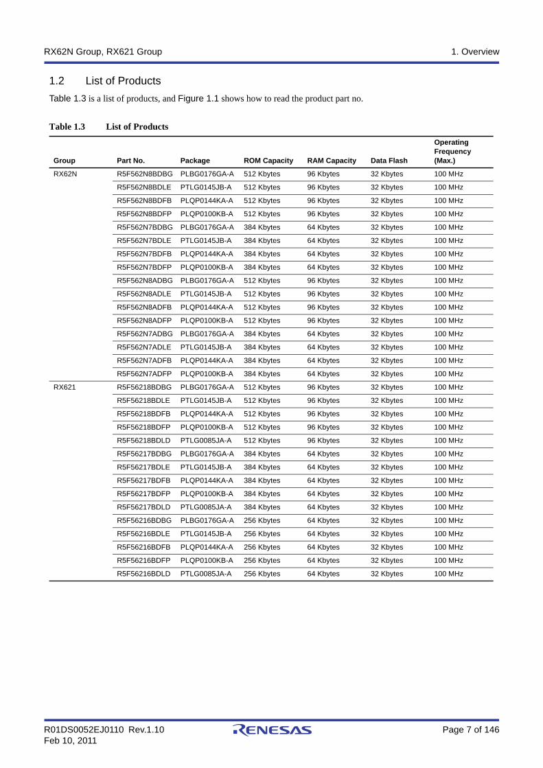
1.2 List of Products
Table 1.3 is a list of products, and Figure 1.1 shows how to read the product part no.
Table 1.3 List of Products
Group Part No. Package ROM Capacity RAM Capacity Data Flash
Operating Frequency (Max.)
RX62N R5F562N8BDBG PLBG0176GA-A 512 Kbytes 96 Kbytes 32 Kbytes 100 MHz
R5F562N8BDLE PTLG0145JB-A 512 Kbytes 96 Kbytes 32 Kbytes 100 MHz
R5F562N8BDFB PLQP0144KA-A 512 Kbytes 96 Kbytes 32 Kbytes 100 MHz
R5F562N8BDFP PLQP0100KB-A 512 Kbytes 96 Kbytes 32 Kbytes 100 MHz
R5F562N7BDBG PLBG0176GA-A 384 Kbytes 64 Kbytes 32 Kbytes 100 MHz
R5F562N7BDLE PTLG0145JB-A 384 Kbytes 64 Kbytes 32 Kbytes 100 MHz
R5F562N7BDFB PLQP0144KA-A 384 Kbytes 64 Kbytes 32 Kbytes 100 MHz
R5F562N7BDFP PLQP0100KB-A 384 Kbytes 64 Kbytes 32 Kbytes 100 MHz
R5F562N8ADBG PLBG0176GA-A 512 Kbytes 96 Kbytes 32 Kbytes 100 MHz
R5F562N8ADLE PTLG0145JB-A 512 Kbytes 96 Kbytes 32 Kbytes 100 MHz
R5F562N8ADFB PLQP0144KA-A 512 Kbytes 96 Kbytes 32 Kbytes 100 MHz
R5F562N8ADFP PLQP0100KB-A 512 Kbytes 96 Kbytes 32 Kbytes 100 MHz
R5F562N7ADBG PLBG0176GA-A 384 Kbytes 64 Kbytes 32 Kbytes 100 MHz
R5F562N7ADLE PTLG0145JB-A 384 Kbytes 64 Kbytes 32 Kbytes 100 MHz
R5F562N7ADFB PLQP0144KA-A 384 Kbytes 64 Kbytes 32 Kbytes 100 MHz
R5F562N7ADFP PLQP0100KB-A 384 Kbytes 64 Kbytes 32 Kbytes 100 MHz
RX621 R5F56218BDBG PLBG0176GA-A 512 Kbytes 96 Kbytes 32 Kbytes 100 MHz
R5F56218BDLE PTLG0145JB-A 512 Kbytes 96 Kbytes 32 Kbytes 100 MHz
R5F56218BDFB PLQP0144KA-A 512 Kbytes 96 Kbytes 32 Kbytes 100 MHz
R5F56218BDFP PLQP0100KB-A 512 Kbytes 96 Kbytes 32 Kbytes 100 MHz
R5F56218BDLD PTLG0085JA-A 512 Kbytes 96 Kbytes 32 Kbytes 100 MHz
R5F56217BDBG PLBG0176GA-A 384 Kbytes 64 Kbytes 32 Kbytes 100 MHz
R5F56217BDLE PTLG0145JB-A 384 Kbytes 64 Kbytes 32 Kbytes 100 MHz
R5F56217BDFB PLQP0144KA-A 384 Kbytes 64 Kbytes 32 Kbytes 100 MHz
R5F56217BDFP PLQP0100KB-A 384 Kbytes 64 Kbytes 32 Kbytes 100 MHz
R5F56217BDLD PTLG0085JA-A 384 Kbytes 64 Kbytes 32 Kbytes 100 MHz
R5F56216BDBG PLBG0176GA-A 256 Kbytes 64 Kbytes 32 Kbytes 100 MHz
R5F56216BDLE PTLG0145JB-A 256 Kbytes 64 Kbytes 32 Kbytes 100 MHz
R5F56216BDFB PLQP0144KA-A 256 Kbytes 64 Kbytes 32 Kbytes 100 MHz
R5F56216BDFP PLQP0100KB-A 256 Kbytes 64 Kbytes 32 Kbytes 100 MHz
R5F56216BDLD PTLG0085JA-A 256 Kbytes 64 Kbytes 32 Kbytes 100 MHz

R01DS0052EJ0110 Rev.1.10 Page 8 of 146Feb 10, 2011
RX62N Group, RX621 Group 1. Overview
Figure 1.1 How to Read the Product Part No.
Indicates the type of memory. F: Flash memory version
R 5
Indicates the package type, number of pins, and pin pitch .BG: LFBGA176-0.80LE: TFLGA145-0.65FB: LQFP144-0.50FP: LQFP100-0.50LD: TFLGA85-0.65
Indicates the ROM capacity, RAM capacity, and data flash capacity.8: 512 Kbytes/96 Kbytes/32 Kbytes7: 384 Kbytes/64 Kbytes/32 Kbytes6: 256 Kbytes/64 Kbytes/32 Kbytes
Indicates a Renesas MCU.
Indicates a Renesas semiconductor product.
A: The CAN module is not included.B: CAN × 1 channel
Indicates a group name2N: RX62N group21: RX621 group
Indicates the RX600 Series.
F 5 6 2 N 7 B D B G

R01DS0052EJ0110 Rev.1.10 Page 9 of 146Feb 10, 2011
RX62N Group, RX621 Group 1. Overview
1.3 Block Diagram
Figure 1.2 shows a block diagram.
Figure 1.2 Block Diagram
Inst
ruct
ion
bus
External bus
Port 0
Port 1
Port 2
Port 4
Port 5
Port 6
Port 7
Port 8
Port 9
Port A
Port B
Port C
Port D
Port EClock
generation circuit
10-bit A/D converter × 4 channels (unit 1)
10-bit A/D converter × 4 channels (unit 0)
12-bit A/D converter × 8 channels
TMR × 2 channels (unit 1)
TMR × 2 channels (unit 0)
MTU × 6 channels (unit 1)
MTU × 6 channels (unit 0)
PPG (unit 1)
PPG (unit 0)
10-bit D/A converter × 2 channels
CMT × 2 channels (unit 1)
SCI × 6ch
WDT
RIIC × 2 channels
Data flash
CRC
CMT × 2 channels (unit 0)
Port F
Port G
IWDT
USB (up to 2 ports)
RSPI (unit 1)
CAN
RTC
RSPI (unit 0)
POE
Notes: 1. The installation of the EXDMAC, EtherC, EDMAC, USB, CAN module, POE, and ports 0 to G is different depending on the product group and package.
2. For detail on the bus configuration of internal peripheral buses, see section 12, Buses. 3. The number of RIIC units and 10-bit D/A converter channels that are incorporated differs with the package.
*1
*1
*1
Port 3*1
Ope
rand
bus
I
nter
nal m
ain
bus
2
ETHERC
EDMAC
ICU
DTC
DMACA
*1
*1
EXDMAC*1
Inte
rnal
per
iphe
ral b
us
1 to
6
BSC
Inte
rnal
ma
in b
us 1
*2
ETHERC: Ethernet controllerEDMAC: DMA controller for Ethernet controllerICU: Interrupt control unitDTC: Data transfer controllerDMACA: DMA controllerEXDMAC: EXDMA controllerBSC: Bus controllerWDT: Watchdog timerIWDT: Independent watchdog timerCRC: CRC (Cyclic Redundancy Check) calculatorMPU: Memory-protection unit
SCI: Serial communications interfacesUSB: USB 2.0 host/function moduleRSPI: Serial peripheral interfacesCAN: CAN moduleMTU: Multi-function timer pulse unitPOE: Port output enablePPG: Programmable pulse generatorTMR: 8-bit timerCMT: Compare match timerRTC: Realtime clockRIIC: I2C bus interface
RX CPU
MPU
RAM
ROM
*3
*3
R01DS0052EJ0110 Rev.1.10 Page 10 of 146Feb 10, 2011
RX62N Group, RX621 Group 1. Overview
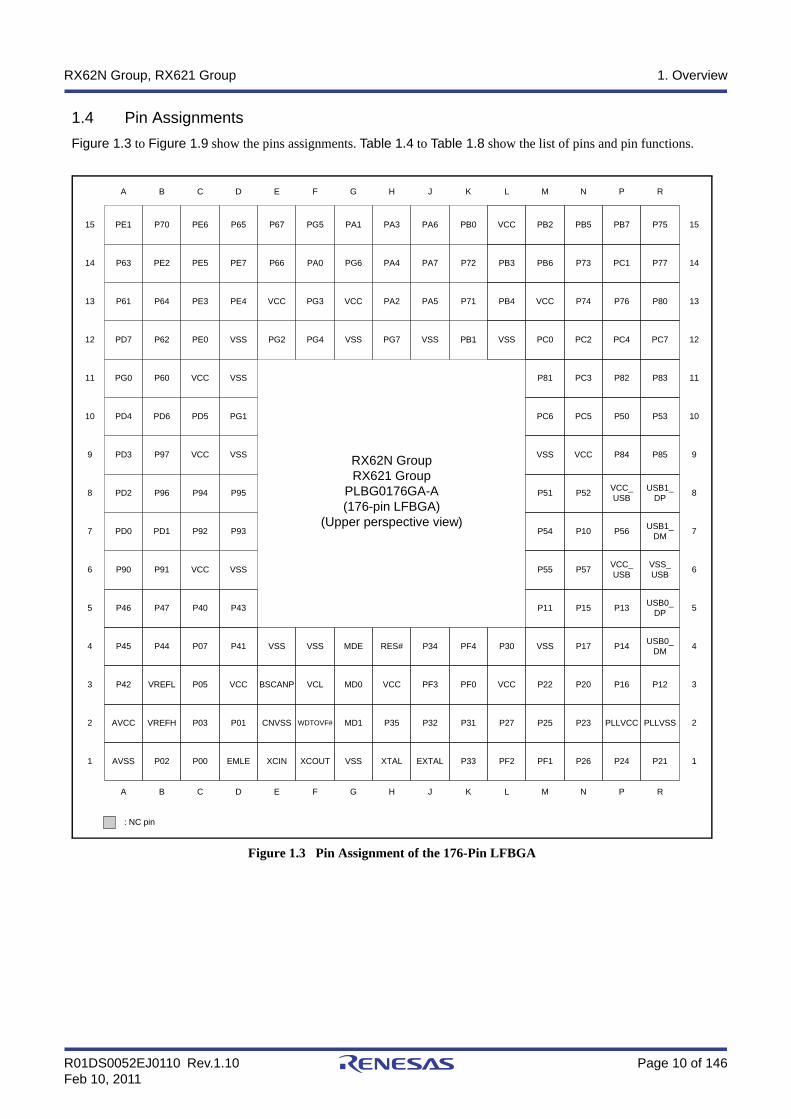
1.4 Pin Assignments
Figure 1.3 to Figure 1.9 show the pins assignments. Table 1.4 to Table 1.8 show the list of pins and pin functions.
Figure 1.3 Pin Assignment of the 176-Pin LFBGA
P70
PE2
P64
P62
P60
PD6
P97
P96
PD1
P91
P47
P44
VREFL
VREFH
P02
PE6
PE5
PE3
PE0
VCC
PD5
VCC
P94
P92
VCC
P40
P07
P05
P03
P00
P65
PE7
PE4
VSS
P41
VCC
P01
EMLE
P67
P66
VCC
VSS
BSCANP
CNVSS
XCIN
PG5
PA0
PG3
VSS
VCL
WDTOVF#
XCOUT
PA1
PG6
VCC
MDE
MD0
MD1
VSS
PA3
PA4
PA2
RES#
VCC
P35
XTAL
PA6
PA7
PA5
P34
PF3
P32
EXTAL
PB0
P72
P71
PF4
PF0
P31
P33
VCC
PB3
PB4
P30
VCC
P27
PF2
PB2
PB6
VCC
PC0
P81
PC6
VSS
P51
P54
P55
P11
VSS
P22
P25
PF1
PB5
P73
P74
PC2
PC3
PC5
VCC
P52
P10
P57
P15
P17
P20
P23
P26
PB7
PC1
P76
PC4
P82
P50
P84
VCC_USB
P56
VCC_USB
P13
P14
P16
PLLVCC
P24
PE1
P63
P61
PD7
PG0
PD4
PD3
PD2
PD0
P90
P46
P45
P42
AVCC
AVSS
P75
P77
P80
PC7
P83
P53
P85
USB1_DP
USB1_DM
VSS_USB
USB0_DP
USB0_DM
P12
PLLVSS
P21
B C D E F G H J K L M N PA R
15
14
13
12
11
10
9
8
7
6
5
4
3
2
1
15
14
13
12
11
10
9
8
7
6
5
4
3
2
1
B C D E F G H J K L M N PA R
RX62N GroupRX621 Group
PLBG0176GA-A(176-pin LFBGA)
(Upper perspective view)
: NC pin
VSSPB1VSSPG7VSSPG4PG2
VSS
PG1
VSS
P95
P93
P43
VSS

R01DS0052EJ0110 Rev.1.10 Page 11 of 146Feb 10, 2011
RX62N Group, RX621 Group 1. Overview
Figure 1.4 Pin Assignment of the 145-Pin TFLGA
NC
RX62N GroupRX621 Group
PTLG0145JB-A(145-pin TFLGA)
(Upper perspective view)
: NC pin
VCL
VSS
P00
BSCANP
P65
P67
PA0
P66
XCIN
XCOUT
WDTOVF#
MDE
PA1
PA3
VCC
PA2
XTAL
VSS
MD1
MD0
VSS
PA5
PA6
PA4
EXTAL
P34
VCC
RES#
PB0
P71
PB1
PA7
P33
P27
P35
P32
PB2
PB4
PB5
P72
P30
P24
P31
P26
P53
VSS
PC7
P82
PC3
PB7
P73
PC0
PB3
P25
P22
P17
P12
VCC_USB
P56
P52
P83
P81
P77
P75
VCC
PB6
P23
P20
PLLVCC
P15
P14
VSS_USB
P55
P50
PC6
P80
PC2
PC1
VSS
P21
P16
PLLVSS
P13
USB0_DM
USB0_DP
P54
P51
VCC
PC5
PC4
P76
P7413
12
11
10
9
8
7
6
5
4
3
2
1
B C D E F G H J K L M NA
B C D E F G H J K L M NA
13
12
11
10
9
8
7
6
5
4
3
2
1P01
P05
VSS
P41
P46
P92
PD2
PD7
P61
P63
PE5
PE3
P70
P03
P07
VREFH
P40
P45
P90
PD1
PD5
VSS
PE0
PE2
PE1
PE4
AVSS
AVCC
VREFL
P42
P44
P47
P91
PD0
PD6
P60
P62
P64
PD3
EMLE
VCC
P02
P43
VCC
VSS
P93
PD4
VCC
VSS
VCC
PE7
PE6

R01DS0052EJ0110 Rev.1.10 Page 12 of 146Feb 10, 2011
RX62N Group, RX621 Group 1. Overview
Figure 1.5 Pin Assignment of the 144-Pin LQFP
1 2 3 4 5 6 7 8 9 10
11
12
13
14
15
16
17
18
19
20
21
22
23
24
25
26
27
28
29
30
31
32
33
34
35
36
10
8
10
7
10
6
10
5
10
4
10
3
10
2
10
1
10
0
99
98
97
96
95
94
93
92
91
90
89
88
87
86
85
84
83
82
81
80
79
78
77
76
75
74
73
72
71
70
69
68
67
66
65
64
63
62
61
60
59
58
57
56
55
54
53
52
51
50
49
48
47
46
45
44
43
42
41
40
39
38
37
109
110
111
112
113
114
115
116
117
118
119
120
121
122
123
124
125
126
127
128
129
130
131
132
133
134
135
136
137
138
139
140
141
142
143
144
PE0/D8/SSLB1-B
P64/CS4#-A/WE#
P63/CS3#-A/CAS#
P62/CS2#-A/RAS#
P61/CS1#-A/SDCS#
VSS
P60/CS0#-A
VCC
PD7/D7/MTIC5U/POE0#
PD6/D6/MTIC5V/POE1#
PD5/D5/MTIC5W/POE2#
PD4/D4/MTIC11U-B/POE3#
PD2/D2/MTIC11W-B/POE5#
PD1/D1/POE6#
PD0/D0/POE7#
P93/A19-B
P92/A18-B
P91/A17-B
VSS
P90/A16-BVCC
P47/AN7/IRQ15-B
P46/AN6/IRQ14
P45/AN5/IRQ13-B
P44/AN4/IRQ12
P43/AN3/IRQ11-B
P42/AN2/IRQ10-B
P41/AN1/IRQ9-B
VREFL
P40/AN0/IRQ8-B
VREFH
P07/ADTRG0#-A/IRQ15-A
PE1/D9/SSLB2-B
PD3/D3/MTIC11V-B/POE4#
AVCC
P74/CS4#-B/ET_ERXD1/RMII_RXD1
PC2/A18-A/MTCLKE-A/RxD5/SSLA3-A/ET_RX_DV
P76/CS6#-B/ET_RX_CLK/REF50CK
P77/CS7#-B/ET_RX_ER/RMII_RX_ER
PC3/A19-A/MTCLKF-A/TxD5/ET_TX_ER
PC4/A20/CS3#-C/MTCLKC-B/SSLA0-A/ET_TX_CLK
P80/EDREQ0-A/MTIOC3B-B/ET_TX_EN/RMII_TXD_EN/TRDATA0
P81/EDACK0-A/MTIOC3D-B/ET_ETXD0/RMII_TXD0/TRDATA1
P82/EDREQ1-A/MTIOC4A-B/ET_ETXD1/RMII_TXD1/TRSYNC
PC5/A21/CS2#-C/WAIT#-C/MTIC11W-A/MTCLKD-B/RSPCKA-A/ET_ETXD2
PC6/A22/CS1#-C/MTIC11V-A/MTCLKA-B/MOSIA-A/ET_ETXD3
PC7/A23/CS0#-B/MTIC11U-A/MTCLKB-B/MISOA-A/ET_COL
VCC
VSS
P50/WR0#/WR#/TxD2-B/SSLB1-A
P51/WR1#/BC1#/WAIT#-D/SCK2/SSLB2-A
P52/RD#/RxD2-B/SSLB3-A
P53/BCLK
P54/EDACK0-C/MTIOC4B-B/ET_LINKSTA/TRDATA2
P55/WAIT#-B/EDREQ0-C/MTIOC4D-B/ET_EXOUT/TRDATA3
P56/EDACK1-C/MTIOC3C-B
VSS_USB
USB0_DP
USB0_DM
VCC_USB
P12/TMCI1-B/RxD2-A/SCL0/IRQ2-B
P13/ADTRG1#/TMO3/TxD2-A/SDA0/IRQ3-B
P14/TMRI2/IRQ4-B/USB0_OVRCURA/USB0_DPUPE-B
P15/PO13/MTIOC0B/TMCI2-A/SCK3-A/IRQ5-B
PLLVSS
P16/PO14/MTIOC3C-A/TMO2/RxD3-A/IRQ6-B/USB0_VBUS/USB0_OVRCURB/USB0_VBUSEN-BPLLVCC
P20/PO0/MTIOC1A/TMRI0-B/TxD0/SDA1/USB0_ID
P75/CS5#-B/ET_ERXD0/RMII_RXD0
P83/EDACK1-A/MTIOC4C-B/ET_CRS/RMII_CRS_DV/TRCLK
P17/PO15/MTIOC3A/TxD3-A/IRQ7-B
PE
3/D
11/P
OE
8#
PE
5/D
13/R
SP
CK
B-B
/IRQ
5-A
VS
S
P70
/SD
CLK
VC
C
PE
6/D
14/M
OS
IB-B
/IRQ
6-A
PE
7/D
15/M
ISO
B-B
/IRQ
7-A
P65
/CS
5#-A
/CK
E
P66
/CS
6#-A
/DQ
M0
P67
/CS
7#-A
/DQ
M1
PA
0/A
0/B
C0#
/PO
16/M
TIO
C6A
/SS
LA
1-B
PA
1/A
1/P
O17
/MT
IOC
6B/S
SLA
2-B
PA
2/A
2/P
O18
/MT
IOC
6C/S
SLA
3-B
VS
S
PA
4/A
4/P
O20
/MT
IOC
7A/S
SLA
0-B
VC
C
PA
5/A
5/P
O21
/MT
IOC
7B/R
SP
CK
A-B
PA
6/A
6/P
O22
/MT
IOC
8A/M
OS
IA-B
PA
7/A
7/P
O23
/MT
IOC
8B/M
ISO
A-B
PB
0/A
8/P
O24
/MT
IOC
9A
P71
/CS
1#-B
/ET
_MD
IO
P72
/CS
2#-B
/ET
_MD
C
PB
1/A
9/P
O25
/MT
IOC
9C
PB
2/A
10/P
O26
/MT
IOC
9B
/MT
CLK
G-B
PB
3/A
11/P
O27
/MT
IOC
9D
/MT
CLK
H-B
PB
4/A
12/P
O28
/MT
IOC
10A
/MT
CL
KE
-B
PB
5/A
13/P
O29
/MT
IOC
10C
/MT
CLK
F-B
PB
6/A
14/P
O30
/MT
IOC
10B
PB
7/A
15/P
O31
/MT
IOC
10D
P73
/CS
3#-B
/ET
_WO
L
VS
S
PC
0/A
16-A
/MT
CLK
G-A
/SS
LA1-
A/E
T_E
RX
D3
PC
1/A
17-A
/MT
CLK
H-A
/SC
K5/
SS
LA2-
A/E
T_E
RX
D2
PE
4/D
12/S
SLB
0-B
PA
3/A
3/P
O19
/MT
IOC
6D
VC
C
AV
SS
VC
C
P03
/DA
0/IR
Q11
-A
VS
S
P02
/TM
CI1
-A/S
CK
6-A
/IRQ
10-A
P01
/TM
CI0
-A/R
xD6
-A/IR
Q9-
A
P00
/TM
RI0
-A/T
xD6
-A/IR
Q8-
A
BS
CA
NP
EM
LE
WD
TO
VF
#
VS
S
MD
E
VC
L
MD
0
XC
IN
XC
OU
TR
ES
#
XT
AL
VS
S
EX
TA
L
VC
C
P35
/NM
I
P34
/PO
12/M
TIO
C0A
/TM
CI3
/SC
K6-
B/IR
Q4-
A/T
RS
T#
P3
2/P
O1
0/M
TIO
C0C
/TxD
6-B
/CT
X0/
IRQ
2-A
/RT
CO
UT
P31
/PO
9/M
TIO
C4D
-A/T
MC
I2-B
/SS
LB0-
A/IR
Q1/
TM
S
P30
/PO
8/M
TIO
C4B
-A/T
MR
I3/R
xD1/
MIS
OB
-A/IR
Q0
/TD
I
P27
/CS
7#-C
/PO
7/M
TIO
C2B
/SC
K1/
RS
PC
KB
-A/T
CK
P26
/CS
6#-C
/PO
6/M
TIO
C2A
/TM
O1/
TxD
1/M
OS
IB-A
/TD
O
P25
/CS
5#-C
/ED
AC
K1
-B/A
DT
RG
0#-B
/PO
5/M
TIO
C4C
-A/M
TC
LKB
-A/R
xD3
-B/U
SB
0_D
PR
PD
P24
/CS
4#-C
/ED
RE
Q1-
B/P
O4/
MT
IOC
4A-A
/MT
CLK
A-A
/TM
RI1
/SC
K3-
B/U
SB
0_V
BU
SE
N-A
P23
/ED
AC
K0-
B/P
O3
/MT
IOC
3D-A
/MT
CLK
D-A
/TxD
3-B
/US
B0_
DP
UP
E-A
P21
/PO
1/M
TIO
C1B
/TM
CI0
-B/R
xD0/
SC
L1/U
SB
0_E
XIC
EN
P05
/DA
1/IR
Q13
-A
MD
1
P22
/ED
RE
Q0-
B/P
O2/
MT
IOC
3B
-A/M
TC
LKC
-A/T
MO
0/S
CK
0/U
SB
0_D
RP
D
P33
/PO
11/M
TIO
C0D
/RxD
6-B
/CR
X0/
IRQ
3-A
PE2/D10/SSLB3-B/POE9#
RX62N GroupRX621 Group
PLQP0144KA-A(144-pin LQFP)
(Top view)
R01DS0052EJ0110 Rev.1.10 Page 13 of 146Feb 10, 2011
RX62N Group, RX621 Group 1. Overview
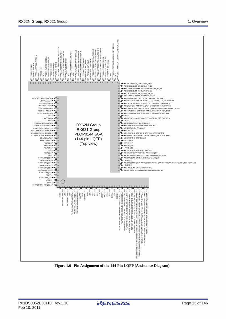
Figure 1.6 Pin Assignment of the 144-Pin LQFP (Assistance Diagram)
P74/CS4#-B/ET_ERXD1/RMII_RXD1
PC2/A18-A/MTCLKE-A/RxD5/SSLA3-A/ET_RX_DV
P76/CS6#-B/ET_RX_CLK/REF50CK
P77/CS7#-B/ET_RX_ER/RMII_RX_ER
PC3/A19-A/MTCLKF-A/TxD5/ET_TX_ER
PC4/A20/CS3#-C/MTCLKC-B/SSLA0-A/ET_TX_CLK
P80/EDREQ0-A/MTIOC3B-B/ET_TX_EN/RMII_TXD_EN/TRDATA0
P81/EDACK0-A/MTIOC3D-B/ET_ETXD0/RMII_TXD0/TRDATA1
P82/EDREQ1-A/MTIOC4A-B/ET_ETXD1/RMII_TXD1/TRSYNC
PC5/A21/CS2#-C/WAIT#-C/MTIC11W-A/MTCLKD-B/RSPCKA-A/ET_ETXD2
PC6/A22/CS1#-C/MTIC11V-A/MTCLKA-B/MOSIA-A/ET_ETXD3
PC7/A23/CS0#-B/MTIC11U-A/MTCLKB-B/MISOA-A/ET_COL
VCC
VSS
P50/WR0#/WR#/TxD2-B/SSLB1-A
P51/WR1#/BC1#/WAIT#-D/SCK2/SSLB2-A
P52/RD#/RxD2-B/SSLB3-A
P53/BCLK
P54/EDACK0-C/MTIOC4B-B/ET_LINKSTA/TRDATA2
P55/WAIT#-B/EDREQ0-C/MTIOC4D-B/ET_EXOUT/TRDATA3
P56/EDACK1-C/MTIOC3C-B
VSS_USB
USB0_DP
USB0_DM
VCC_USB
P12/TMCI1-B/RxD2-A/SCL0/IRQ2-B
P13/ADTRG1#/TMO3/TxD2-A/SDA0/IRQ3-B
P14/TMRI2/IRQ4-B/USB0_OVRCURA/USB0_DPUPE-B
P15/PO13/MTIOC0B/TMCI2-A/SCK3-A/IRQ5-B
PLLVSS
P16/PO14/MTIOC3C-A/TMO2/RxD3-A/IRQ6-B/USB0_VBUS/USB0_OVRCURB/USB0_VBUSEN-BPLLVCC
P20/PO0/MTIOC1A/TMRI0-B/TxD0/SDA1/USB0_ID
P75/CS5#-B/ET_ERXD0/RMII_RXD0
P83/EDACK1-A/MTIOC4C-B/ET_CRS/RMII_CRS_DV/TRCLK
P17/PO15/MTIOC3A/TxD3-A/IRQ7-B
PE
3/D
11/P
OE
8#
PE
5/D
13/R
SP
CK
B-B
/IRQ
5-A
VS
S
P7
0/S
DC
LK
VC
C
PE
6/D
14/M
OS
IB-B
/IRQ
6-A
PE
7/D
15/M
ISO
B-B
/IRQ
7-A
P6
5/C
S5#
-A/C
KE
P6
6/C
S6#
-A/D
QM
0
P6
7/C
S7#
-A/D
QM
1
PA
0/A
0/B
C0#
/PO
16/M
TIO
C6A
/SS
LA
1-B
PA
1/A
1/P
O17
/MT
IOC
6B/S
SLA
2-B
PA
2/A
2/P
O18
/MT
IOC
6C/S
SLA
3-B
VS
S
PA
4/A
4/P
O20
/MT
IOC
7A/S
SLA
0-B
VC
C
PA
5/A
5/P
O21
/MT
IOC
7B/R
SP
CK
A-B
PA
6/A
6/P
O22
/MT
IOC
8A/M
OS
IA-B
PA
7/A
7/P
O23
/MT
IOC
8B/M
ISO
A-B
PB
0/A
8/P
O24
/MT
IOC
9A
P7
1/C
S1#
-B/E
T_M
DIO
P7
2/C
S2#
-B/E
T_M
DC
PB
1/A
9/P
O25
/MT
IOC
9C
PB
2/A
10/P
O26
/MT
IOC
9B
/MT
CLK
G-B
PB
3/A
11/P
O27
/MT
IOC
9D
/MT
CLK
H-B
PB
4/A
12/P
O28
/MT
IOC
10
A/M
TC
LK
E-B
PB
5/A
13/P
O29
/MT
IOC
10
C/M
TC
LK
F-B
PB
6/A
14/P
O30
/MT
IOC
10
B
PB
7/A
15/P
O31
/MT
IOC
10
D
P7
3/C
S3#
-B/E
T_W
OL
VS
S
PC
0/A
16-A
/MT
CL
KG
-A/S
SLA
1-A
/ET
_ER
XD
3
PC
1/A
17-A
/MT
CL
KH
-A/S
CK
5/S
SLA
2-A
/ET
_ER
XD
2
PE
4/D
12/S
SLB
0-B
PA
3/A
3/P
O19
/MT
IOC
6D
VC
C
1 2 3 4 5 6 7 8 9 10
11
12
13
14
15
16
17
18
19
20
21
22
23
24
25
26
27
28
29
30
31
32
33
34
35
36
109
110
111
112
113
114
115
116
117
118
119
120
121
122
123
124
125
126
127
128
129
130
131
132
133
134
135
136
137
138
139
140
141
142
143
144
PE0/D8/SSLB1-B
P64/CS4#-A/WE#
P63/CS3#-A/CAS#
P62/CS2#-A/RAS#
P61/CS1#-A/SDCS#
VSS
P60/CS0#-A
VCC
PD7/D7/MTIC5U/POE0#
PD6/D6/MTIC5V/POE1#
PD5/D5/MTIC5W/POE2#
PD4/D4/MTIC11U-B/POE3#
PD2/D2/MTIC11W-B/POE5#
PD1/D1/POE6#PD0/D0/POE7#
P93/A19-B
P92/A18-B
P91/A17-B
VSS
P90/A16-BVCC
P47/AN7/IRQ15-B
P46/AN6/IRQ14
P45/AN5/IRQ13-B
P44/AN4/IRQ12
P43/AN3/IRQ11-B
P42/AN2/IRQ10-B
P41/AN1/IRQ9-B
VREFL
P40/AN0/IRQ8-B
VREFH
P07/ADTRG0#-A/IRQ15-A
PE1/D9/SSLB2-B
PD3/D3/MTIC11V-B/POE4#
AVCC
AV
SS
VC
C
P03
/DA
0/IR
Q11
-A
VS
S
P02
/TM
CI1
-A/S
CK
6-A
/IRQ
10-A
P0
1/T
MC
I0-A
/RxD
6-A
/IRQ
9-A
P00
/TM
RI0
-A/T
xD6
-A/IR
Q8-
A
BS
CA
NP
EM
LE
WD
TO
VF
#
VS
S
MD
E
VC
L
MD
0
RE
S#
XT
AL
VS
S
EX
TA
L
VC
C
P34
/PO
12/M
TIO
C0A
/TM
CI3
/SC
K6
-B/IR
Q4-
A/T
RS
T#
P31
/PO
9/M
TIO
C4D
-A/T
MC
I2-B
/SS
LB
0-A
/IRQ
1/T
MS
P30
/PO
8/M
TIO
C4B
-A/T
MR
I3/R
xD1/
MIS
OB
-A/I
RQ
0/T
DI
P27
/CS
7#-C
/PO
7/M
TIO
C2B
/SC
K1
/RS
PC
KB
-A/T
CK
P26
/CS
6#
-C/P
O6/
MT
IOC
2A/T
MO
1/T
xD1/
MO
SIB
-A/T
DO
P2
5/C
S5#
-C/E
DA
CK
1-B
/AD
TR
G0
#-B
/PO
5/M
TIO
C4
C-A
/MT
CL
KB
-A/R
xD3-
B/U
SB
0_D
PR
PD
P2
4/C
S4
#-C
/ED
RE
Q1-
B/P
O4/
MT
IOC
4A-A
/MT
CL
KA
-A/T
MR
I1/S
CK
3-B
/US
B0_
VB
US
EN
-A
P23
/ED
AC
K0-
B/P
O3
/MT
IOC
3D-A
/MT
CLK
D-A
/TxD
3-B
/US
B0_
DP
UP
E-A
P21
/PO
1/M
TIO
C1
B/T
MC
I0-B
/RxD
0/S
CL1
/US
B0_
EX
ICE
N
P05
/DA
1/IR
Q13
-A
MD
1
P22
/ED
RE
Q0-
B/P
O2/
MT
IOC
3B
-A/M
TC
LK
C-A
/TM
O0/
SC
K0/
US
B0_
DR
PD
PE2/D10/SSLB3-B/POE9#
P35
/NM
I
P33
/PO
11/M
TIO
C0
D/R
xD6
-B/C
RX
0/IR
Q3-
A
P3
2/P
O1
0/M
TIO
C0C
/TxD
6-B
/CT
X0
/IR
Q2-
A/R
TC
OU
T
72
71
70
69
68
67
66
65
64
63
62
61
60
59
58
57
56
55
54
53
52
51
50
49
48
47
46
45
44
43
42
41
40
39
38
37
RX62N GroupRX621 Group
PLQP0144KA-A(144-pin LQFP)
(Top view)
108
107
106
105
104
103
102
101
100
99
98
97
96
95
94
93
92
91
90
89
88
87
86
85
84
83
82
81
80
79
78
77
76
75
74
73
XC
IN
XC
OU
T
R01DS0052EJ0110 Rev.1.10 Page 14 of 146Feb 10, 2011
RX62N Group, RX621 Group 1. Overview
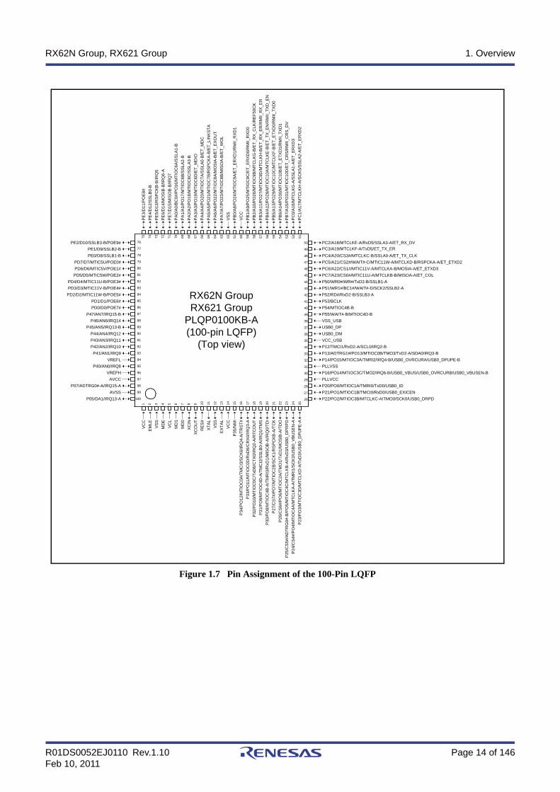
Figure 1.7 Pin Assignment of the 100-Pin LQFP
1 2 3 4 5 6 7 8 9 10 11 12 13 14 15 16 17 18 19 20 21 22 23 24 25
75 74 73 72 71 70 69 68 67 66 65 64 63 62 61 60 59 58 57 56 55 54 53 52 51
50
49
48
47
46
45
44
43
42
41
40
39
38
37
36
35
34
33
32
31
30
29
28
27
26
76
77
78
79
80
81
82
83
84
85
86
87
88
89
90
91
92
93
94
95
96
97
98
99
100
PE0/D8/SSLB1-B
PD7/D7/MTIC5U/POE0#
PD6/D6/MTIC5V/POE1#
PD5/D5/MTIC5W/POE2#
PD4/D4/MTIC11U-B/POE3#
PD3/D3/MTIC11V-B/POE4#
PD2/D2/MTIC11W-B/POE5#
PD1/D1/POE6#
PD0/D0/POE7#
P47/AN7/IRQ15-B
P46/AN6/IRQ14
P45/AN5/IRQ13-B
P43/AN3/IRQ11
P42/AN2/IRQ10
P41/AN1/IRQ9
VREFL
P40/AN0/IRQ8
VREFH
AVCC
P07/ADTRG0#-A/IRQ15-A
AVSS
PE1/D9/SSLB2-B
P44/AN4/IRQ12
PC2/A18/MTCLKE-A/RxD5/SSLA3-A/ET_RX_DV
PC4/A20/CS3#/MTCLKC-B/SSLA0-A/ET_TX_CLK
PC5/A21/CS2#/WAIT#-C/MTIC11W-A/MTCLKD-B/RSPCKA-A/ET_ETXD2
PC6/A22/CS1#/MTIC11V-A/MTCLKA-B/MOSIA-A/ET_ETXD3
PC7/A23/CS0#/MTIC11U-A/MTCLKB-B/MISOA-A/ET_COL
P50/WR0#/WR#/TxD2-B/SSLB1-A
P51/WR1#/BC1#/WAIT#-D/SCK2/SSLB2-A
P52/RD#/RxD2-B/SSLB3-A
P53/BCLK
P54/MTIOC4B-B
P55/WAIT#-B/MTIOC4D-B
VSS_USB
USB0_DP
VCC_USB
P12/TMCI1/RxD2-A/SCL0/IRQ2-B
P13/ADTRG1#/PO13/MTIOC0B/TMO3/TxD2-A/SDA0/IRQ3-B
P14/PO15/MTIOC3A/TMRI2/IRQ4-B/USB0_OVRCURA/USB0_DPUPE-B
PLLVSS
P16/PO14/MTIOC3C/TMO2/IRQ6-B/USB0_VBUS/USB0_OVRCURB/USB0_VBUSEN-B
PLLVCC
P20/PO0/MTIOC1A/TMRI0/TxD0/USB0_ID
P21/PO1/MTIOC1B/TMCI0/RxD0/USB0_EXICEN
P22/PO2/MTIOC3B/MTCLKC-A/TMO0/SCK0/USB0_DRPD
PC3/A19/MTCLKF-A/TxD5/ET_TX_ER
USB0_DM
PE
3/D
11/P
OE
8#
PE
5/D
13/R
SP
CK
B-B
/IRQ
5
PE
6/D
14/M
OS
IB-B
/IRQ
6-A
PE
7/D
15/M
ISO
B-B
/IRQ
7
PA
0/A
0/B
C0#
/PO
16/M
TIO
C6A
/SS
LA1-
B
PA
1/A
1/P
O17
/MT
IOC
6B
/SS
LA2-
B
PA
2/A
2/P
O18
/MT
IOC
6C
/SS
LA
3-B
PA
3/A
3/P
O19
/MT
IOC
6D
/ET
_M
DIO
PA
4/A
4/P
O20
/MT
IOC
7A
/SS
LA0-
B/E
T_
MD
C
PA
5/A
5/P
O21
/MT
IOC
7B
/RS
PC
KA
-B/E
T_L
INK
ST
A
PA
6/A
6/P
O22
/MT
IOC
8A
/MO
SIA
-B/E
T_E
XO
UT
PA
7/A
7/P
O23
/MT
IOC
8B
/MIS
OA
-B/E
T_W
OL
VS
S
VC
C
PB
1/A
9/P
O25
/MT
IOC
9C
/ET
_E
RX
D0/
RM
II_R
XD
0
PB
2/A
10/P
O2
6/M
TIO
C9B
/MT
CL
KG
-B/E
T_R
X_C
LK/R
EF
50C
K
PB
3/A
11/P
O2
7/M
TIO
C9D
/MT
CL
KH
-B/E
T_R
X_E
R/R
MII_
RX
_ER
PB
4/A
12/P
O2
8/M
TIO
C10
A/M
TC
LKE
-B/E
T_
TX
_EN
/RM
II_T
XD
_EN
PB
5/A
13/P
O2
9/M
TIO
C10
C/M
TC
LKF
-B/E
T_
ET
XD
0/R
MII_
TX
D0
PB
6/A
14/P
O3
0/M
TIO
C10
B/E
T_E
TX
D1
/RM
II_T
XD
1
PB
7/A
15/P
O3
1/M
TIO
C10
D/E
T_C
RS
/RM
II_C
RS
_DV
PC
0/A
16/M
TC
LKG
-A/S
SLA
1-A
/ET
_ER
XD
3
PC
1/A
17/M
TC
LKH
-A/S
CK
5/S
SLA
2-A
/ET
_E
RX
D2
PE
4/D
12/S
SL
B0-
B
PB
0/A
8/P
O24
/MT
IOC
9A
/ET
_ER
XD
1/R
MII
_RX
D1
VC
C
VS
S
MD
E
VC
L
MD
1
MD
0
RE
S#
XT
AL
VS
S
EX
TA
L
P35
/NM
I
P34
/PO
12/M
TIO
C0A
/TM
CI3
/SC
K6/
IRQ
4-A
/TR
ST
#
P3
3/P
O1
1/M
TIO
C0D
/RxD
6/C
RX
0/IR
Q3-
A
P32
/PO
10/
MT
IOC
0C/T
xD6/
CT
X0/
IRQ
2-A
/RT
CO
UT
P31
/PO
9/M
TIO
C4D
-A/T
MC
I2/S
SLB
0-A
/IRQ
1/T
MS
P30
/PO
8/M
TIO
C4B
-A/T
MR
I3/R
xD1/
MIS
OB
-A/IR
Q0/
TD
I
P27
/CS
7#/P
O7/
MT
IOC
2B
/SC
K1
/RS
PC
KB
-A/T
CK
P26
/CS
6#/P
O6
/MT
IOC
2A
/TM
O1/
TxD
1/M
OS
IB-A
/TD
O
P25
/CS
5#/A
DT
RG
0#-B
/PO
5/M
TIO
C4C
/MT
CLK
B-A
/RxD
3/U
SB
0_D
PR
PD
P23
/PO
3/M
TIO
C3D
/MT
CLK
D-A
/TxD
3/U
SB
0_D
PU
PE
-A
EM
LE
VC
C
PE2/D10/SSLB3-B/POE9#
P05/DA1/IRQ13-A
P24
/CS
4#/P
O4/
MT
IOC
4A/M
TC
LKA
-A/T
MR
I1/S
CK
3/U
SB
0_V
BU
SE
N-A
RX62N GroupRX621 Group
PLQP0100KB-A(100-pin LQFP)
(Top view)
XC
IN
XC
OU
T

R01DS0052EJ0110 Rev.1.10 Page 15 of 146Feb 10, 2011
RX62N Group, RX621 Group 1. Overview
Figure 1.8 Pin Assignment of the 100-Pin LQFP (Assistance Diagram)
1 2 3 4 5 6 7 8 9 10 11 12 13 14 15 16 17 18 19 20 21 22 23 24 25
P31
/PO
9/M
TIO
C4D
-A/T
MC
I2/S
SL
B0-
A/IR
Q1/
TM
S
76
77
78
79
80
81
82
83
84
85
86
87
88
89
90
91
92
93
94
95
96
97
98
99
100
PE0/D8/SSLB1-B
PD7/D7/MTIC5U/POE0#
PD6/D6/MTIC5V/POE1#
PD5/D5/MTIC5W/POE2#
PD4/D4/MTIC11U-B/POE3#
PD3/D3/MTIC11V-B/POE4#
PD2/D2/MTIC11W-B/POE5#
PD1/D1/POE6#
PD0/D0/POE7#
P47/AN7/IRQ15-B
P46/AN6/IRQ14
P45/AN5/IRQ13-B
P43/AN3/IRQ11
P42/AN2/IRQ10
P41/AN1/IRQ9
VREFL
P40/AN0/IRQ8
VREFH
AVCC
P07/ADTRG0#-A/IRQ15-A
AVSS
PE1/D9/SSLB2-B
P44/AN4/IRQ12
VC
C
VS
S
MD
E
VC
L
MD
1
MD
0
RE
S#
XT
AL
VS
S
EX
TA
L
P34
/PO
12/M
TIO
C0A
/TM
CI3
/SC
K6/
IRQ
4-A
/TR
ST
#
P30
/PO
8/M
TIO
C4B
-A/T
MR
I3/R
xD1/
MIS
OB
-A/I
RQ
0/T
DI
P27
/CS
7#/P
O7/
MT
IOC
2B
/SC
K1/
RS
PC
KB
-A/T
CK
P26
/CS
6#/P
O6/
MT
IOC
2A/T
MO
1/T
xD1/
MO
SIB
-A/T
DO
P25
/CS
5#/A
DT
RG
0#-B
/PO
5/M
TIO
C4C
/MT
CL
KB
-A/R
xD3/
US
B0_
DP
RP
D
P2
3/P
O3/
MT
IOC
3D/M
TC
LKD
-A/T
xD3
/US
B0_
DP
UP
E-A
EM
LE
VC
C
PE2/D10/SSLB3-B/POE9#
P05/DA1/IRQ13-A
P2
4/C
S4#
/PO
4/M
TIO
C4A
/MT
CLK
A-A
/TM
RI1
/SC
K3
/US
B0_
VB
US
EN
-A
75 74 73 72 71 70 69 68 67 66 65 64 63 62 61 60 59 58 57 56 55 54 53 52 51
50
49
48
47
46
45
44
43
42
41
40
39
38
37
36
35
34
33
32
31
30
29
28
27
26
PC2/A18/MTCLKE-A/RxD5/SSLA3-A/ET_RX_DV
PC4/A20/CS3#/MTCLKC-B/SSLA0-A/ET_TX_CLK
PC5/A21/CS2#/WAIT#-C/MTIC11W-A/MTCLKD-B/RSPCKA-A/ET_ETXD2
PC6/A22/CS1#/MTIC11V-A/MTCLKA-B/MOSIA-A/ET_ETXD3
PC7/A23/CS0#/MTIC11U-A/MTCLKB-B/MISOA-A/ET_COL
P50/WR0#/WR#/TxD2-B/SSLB1-A
P51/WR1#/BC1#/WAIT#-D/SCK2/SSLB2-A
P52/RD#/RxD2-B/SSLB3-A
P53/BCLK
P54/MTIOC4B-B
P55/WAIT#-B/MTIOC4D-B
VSS_USB
USB0_DP
VCC_USB
P12/TMCI1/RxD2-A/SCL0/IRQ2-B
P13/ADTRG1#/PO13/MTIOC0B/TMO3/TxD2-A/SDA0/IRQ3-B
P14/PO15/MTIOC3A/TMRI2/IRQ4-B/USB0_OVRCURA/USB0_DPUPE-B
PLLVSS
P16/PO14/MTIOC3C/TMO2/IRQ6-B/USB0_VBUS/USB0_OVRCURB/USB0_VBUSEN-B
PLLVCC
P20/PO0/MTIOC1A/TMRI0/TxD0/USB0_ID
P21/PO1/MTIOC1B/TMCI0/RxD0/USB0_EXICEN
P22/PO2/MTIOC3B/MTCLKC-A/TMO0/SCK0/USB0_DRPD
PC3/A19/MTCLKF-A/TxD5/ET_TX_ER
USB0_DM
PE
3/D
11
/PO
E8
#
PE
5/D
13
/RS
PC
KB
-B/IR
Q5
PE
6/D
14
/MO
SIB
-B/IR
Q6-
A
PE
7/D
15
/MIS
OB
-B/IR
Q7
PA
0/A
0/B
C0
#/P
O16
/TIO
C6A
/SS
LA1-
B
PA
1/A
1/P
O17
/MT
IOC
6B
/SS
LA2-
B
PA
2/A
2/P
O18
/MT
IOC
6C
/SS
LA
3-B
PA
3/A
3/P
O19
/MT
IOC
6D
/ET
_M
DIO
PA
4/A
4/P
O20
/MT
IOC
7A
/SS
LA0-
B/E
T_
MD
C
PA
5/A
5/P
O21
/MT
IOC
7B
/RS
PC
KA
-B/E
T_L
INK
ST
A
PA
6/A
6/P
O22
/MT
IOC
8A
/MO
SIA
-B/E
T_E
XO
UT
PA
7/A
7/P
O23
/MT
IOC
8B
/MIS
OA
-B/E
T_W
OL
VS
S
VC
C
PB
1/A
9/P
O25
/MT
IOC
9C
/ET
_E
RX
D0/
RM
II_
RX
D0
PB
2/A
10/P
O2
6/M
TIO
C9B
/MT
CL
KG
-B/E
T_R
X_C
LK
/RE
F50
CK
PB
3/A
11/
PO
27/
MT
IOC
9D/M
TC
LK
H-B
/ET
_RX
_ER
/RM
II_R
X_E
R
PB
4/A
12/P
O2
8/M
TIO
C10
A/M
TC
LKE
-B/E
T_T
X_E
N/R
MII
_TX
D_E
N
PB
5/A
13/
PO
29/
MT
IOC
10C
/MT
CLK
F-B
/ET
_E
TX
D0/
RM
II_T
XD
0
PB
6/A
14/P
O3
0/M
TIO
C10
B/E
T_E
TX
D1
/RM
II_T
XD
1
PB
7/A
15/P
O3
1/M
TIO
C10
D/E
T_C
RS
/RM
II_C
RS
_DV
PC
0/A
16
/MT
CLK
G-A
/SS
LA1-
A/E
T_
ER
XD
3
PC
1/A
17
/MT
CLK
H-A
/SC
K5/
SS
LA2-
A/E
T_
ER
XD
2
PE
4/D
12
/SS
LB
0-B
PB
0/A
8/P
O24
/MT
IOC
9A
/ET
_ER
XD
1/R
MII
_RX
D1
P35
/NM
I
P3
2/P
O1
0/M
TIO
C0C
/TxD
6/C
TX
0/IR
Q2-
A/R
TC
OU
T
P33
/PO
11/M
TIO
C0
D/R
xD6
/CR
X0
/IRQ
3-A
RX62N GroupRX621 Group
PLQP0100KB-A(100-pin LQFP)
(Top view)
XC
IN
XC
OU
T
R01DS0052EJ0110 Rev.1.10 Page 16 of 146Feb 10, 2011
RX62N Group, RX621 Group 1. Overview
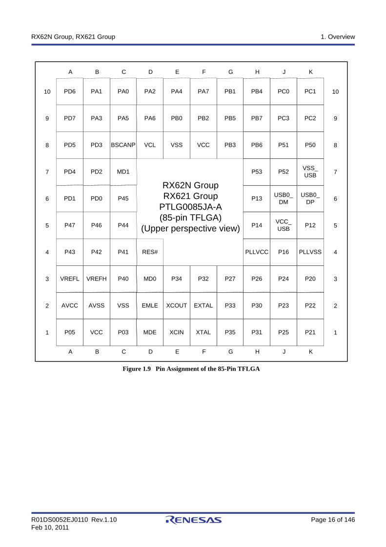
Figure 1.9 Pin Assignment of the 85-Pin TFLGA
RX62N GroupRX621 Group
PTLG0085JA-A(85-pin TFLGA)
(Upper perspective view)
P05
AVCC
VREFL
P43
P47
PD1
PD4
VCC
AVSS
VREFH
P42
P46
PD0
PD2
P03
VSS
P40
P41
P44
P45
MD1
MDE
EMLE
MD0
RES#
XCIN
XCOUT
P34
XTAL
EXTAL
P32
P35
P33
P27
P31
P30
P26
PLLVCC
P14
P13
P53
P25
P23
P24
P16
VCC_USB
USB0_DM
P52
P21
P22
P20
PLLVSS
P12
USB0_DP
VSS_USB
10
9
8
7
6
5
4
3
2
1
10
9
8
7
6
5
4
3
2
1
B C D E F G H J KA
B C D E F G H J KA
PD5
PD7
PD6
PD3
PA3
PA1
BSCANP
PA5
PA0
VCL
PA6
PA2
VSS
PB0
PA4
VCC
PB2
PA7
PB3
PB5
PB1
PB6
PB7
PB4
P51
PC3
PC0
P50
PC2
PC1

R01DS0052EJ0110 Rev.1.10 Page 17 of 146Feb 10, 2011
RX62N Group, RX621 Group 1. Overview
Table 1.4 List of Pins and Pin Functions (176-Pin LFBGA) (1 / 6)
Pin No. Power SupplyClockSystem Control
I/O Port
External BusEXDMAC
ETHERCEDMAC USB
Timers(MTU, TMR, PPG, POE, WDT)
Communi-cation(SCI, CAN, RSPI, RIIC) Others
176-Pin LFBGA
A1 AVSS
A2 AVCC
A3 P42 IRQ10-B/AN2
A4 P45 IRQ13-B/AN5
A5 P46 IRQ14/AN6
A6 P90 D16/A16-B
A7 PD0 D0 POE7#
A8 PD2 D2 MTIC11W-B/POE5#
A9 PD3 D3 MTIC11V-B/POE4#
A10 PD4 D4 MTIC11U-B/POE3#
A11 PG0 D24
A12 PD7 D7 MTIC5U-B/POE0#
A13 P61 CS1#-A/SDCS#
A14 P63 CS3#-A/CAS#
A15 PE1 D9 SSLB2-B
B1 P02 TMCI1-A SCK6-A IRQ10-A
B2 VREFH
B3 VREFL
B4 P44 IRQ12/AN4
B5 P47 IRQ15-B/AN7
B6 P91 D17/A17-B
B7 PD1 D1 POE6#
B8 P96 D22/A22-B
B9 P97 D23/A23-B
B10 PD6 D6 MTIC5V-B/POE1#
B11 P60 CS0#-A
B12 P62 CS2#-A/RAS#
B13 P64 CS4#-A/WE#
B14 PE2 D10 POE9# SSLB3-B
B15 SDCLK P70
C1 P00 TMRI0-A TxD6-A IRQ8-A
C2 P03 IRQ11-A/DA0
C3 P05 IRQ13-A/DA1
C4 P07 IRQ15-A/ADTRG0#-A
C5 P40 IRQ8-B/AN0
R01DS0052EJ0110 Rev.1.10 Page 18 of 146Feb 10, 2011
RX62N Group, RX621 Group 1. Overview
C6 VCC
C7 P92 D18/A18-B
C8 P94 D20/A20-B
C9 VCC
C10 PD5 D5 MTIC5W-B/POE2#
C11 VCC
C12 PE0 D8 SSLB1-B
C13 PE3 D11 POE8#
C14 PE5 D13 RSPCKB-B IRQ5-A
C15 PE6 D14 MOSIB-B IRQ6-A
D1 EMLE
D2 P01 TMCI0-A RxD6-A IRQ9-A
D3 VCC
D4 P41 IRQ9-B/AN1
D5 P43 IRQ11-B/AN3
D6 VSS
D7 P93 D19/A19-B
D8 P95 D21/A21-B
D9 VSS
D10 PG1 D25
D11 VSS
D12 VSS
D13 PE4 D12 SSLB0-B
D14 PE7 D15 MISOB-B IRQ7-A
D15 P65 CS5#-A/CKE
E1 XCIN
E2 CNVSS
E3 BSCANP
E4 VSS
E12 PG2 D26 TRDATA0
E13 VCC
E14 P66 CS6#-A/DQM0
E15 P67 CS7#-A/DQM1
F1 XCOUT
F2 WDTOVF#
F3 VCL
F4 VSS
F12 PG4 D28 TRSYNC
F13 PG3 D27 TRDATA1
F14 PA0 A0/BC0#/DQM2
MTIOC6A/PO16
SSLA1-B
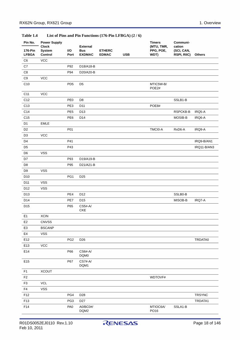
Table 1.4 List of Pins and Pin Functions (176-Pin LFBGA) (2 / 6)
Pin No. Power SupplyClockSystem Control
I/O Port
External BusEXDMAC
ETHERCEDMAC USB
Timers(MTU, TMR, PPG, POE, WDT)
Communi-cation(SCI, CAN, RSPI, RIIC) Others
176-Pin LFBGA

R01DS0052EJ0110 Rev.1.10 Page 19 of 146Feb 10, 2011
RX62N Group, RX621 Group 1. Overview
F15 PG5 D29 TRCLK
G1 VSS
G2 MD1
G3 MD0
G4 MDE
G12 VSS
G13 VCC
G14 PG6 D30 TRDATA2
G15 PA1 A1/DQM3 MTIOC6B/PO17
SSLA2-B
H1 XTAL
H2 P35 NMI
H3 VCC
H4 RES#
H12 PG7 D31 TRDATA3
H13 PA2 A2 MTIOC6C/PO18
SSLA3-B
H14 PA4 A4 MTIOC7A/PO20
SSLA0-B
H15 PA3 A3 MTIOC6D/PO19
J1 EXTAL
J2 P32 MTIOC0C/PO10/RTCOUT
CTX0/TxD6-B
IRQ2-A
J3 PF3 TMS
J4 P34 MTIOC0A/TMCI3-B/PO12
SCK6-B IRQ4-A
J12 VSS
J13 PA5 A5 MTIOC7B/PO21
RSPCKA-B
J14 PA7 A7 MTIOC8B/PO23
MISOA-B
J15 PA6 A6 MTIOC8A/PO22
MOSIA-B
K1 P33 MTIOC0D/PO11
CRX0/RxD6-B
IRQ3-A
K2 P31 USB1_DPRPD MTIOC4D-A/TMCI2-B/PO9
SSLB0-A IRQ1-A
K3 PF0 TxD1-B TDO
K4 PF4 TRST#
K12 PB1 A9 MTIOC9C/PO25
K13 P71 CS1#-B ET_MDIO
K14 P72 CS2#-B ET_MDC
Table 1.4 List of Pins and Pin Functions (176-Pin LFBGA) (3 / 6)
Pin No. Power SupplyClockSystem Control
I/O Port
External BusEXDMAC
ETHERCEDMAC USB
Timers(MTU, TMR, PPG, POE, WDT)
Communi-cation(SCI, CAN, RSPI, RIIC) Others
176-Pin LFBGA

R01DS0052EJ0110 Rev.1.10 Page 20 of 146Feb 10, 2011
RX62N Group, RX621 Group 1. Overview
K15 PB0 A8 MTIOC9A/PO24
L1 PF2 RxD1-B TDI
L2 P27 CS7#-C USB1_EXICEN MTIOC2B/PO7
RSPCKB-A/SCK1-A
L3 VCC
L4 P30 USB1_DRPD MTIOC4B-A/TMRI3-B/PO8
MISOB-A/RxD1-A
IRQ0-A
L12 VSS
L13 PB4 A12 MTIOC10A/MTCLKE-B/PO28
L14 PB3 A11 MTIOC9D/MTCLKH-B/PO27
L15 VCC
M1 PF1 SCK1-B TCK
M2 P25 CS5#-C/EDACK1-B
USB0_DPRPD MTIOC4C-A/MTCLKB-A/PO5
RxD3-B ADTRG0#-B
M3 P22 EDREQ0-B USB0_DRPD MTIOC3B-A/MTCLKC-A/TMO0/PO2
SCK0
M4 VSS
M5 P11 USB1_VBUSEN-A
MTIC5V-A/TMCI3-A
SCK2-A IRQ1-B
M6 P55 WAIT#-B/EDREQ0-C
ET_EXOUT MTIOC4D-B
M7 P54 EDACK0-C ET_LINKSTA MTIOC4B-B
M8 P51 WR1#/BC1#/WAIT#-D
SSLB2-A/SCK2-B
M9 VSS
M10 PC6 A22-A/CS1#-C
ET_ETXD3 MTIC11V-A/MTCLKA-B
MOSIA-A
M11 P81 EDACK0-A ET_ETXD0/RMII_TXD0
MTIOC3D-B
M12 PC0 A16-A ET_ERXD3 MTCLKG-A SSLA1-A
M13 VCC
M14 PB6 A14 MTIOC10B/PO30
M15 PB2 A10 MTIOC9B/MTCLKG-B/PO26
N1 P26 CS6#-C USB1_ID MTIOC2A/TMO1/PO6
MOSIB-A/TxD1-A
Table 1.4 List of Pins and Pin Functions (176-Pin LFBGA) (4 / 6)
Pin No. Power SupplyClockSystem Control
I/O Port
External BusEXDMAC
ETHERCEDMAC USB
Timers(MTU, TMR, PPG, POE, WDT)
Communi-cation(SCI, CAN, RSPI, RIIC) Others
176-Pin LFBGA

R01DS0052EJ0110 Rev.1.10 Page 21 of 146Feb 10, 2011
RX62N Group, RX621 Group 1. Overview
N2 P23 EDACK0-B USB0_DPUPE-A
MTIOC3D-A/MTCLKD-A/PO3
TxD3-B
N3 P20 USB0_ID MTIOC1A/TMRI0-B/PO0
SDA1/TxD0
N4 P17 USB1_VBUS/USB1_OVRCURB/USB1_VBUSEN-B
MTIOC3A/PO15
TxD3-A IRQ7-B
N5 P15 USB1_OVRCURA/USB1_DPUPE-B
MTIOC0B/TMCI2-A/PO13
SCK3-A IRQ5-B
N6 P57 WAIT#-A/WR3#/BC3#/EDREQ1-C
N7 P10 USB1_DPUPE-A
MTIC5W-A/TMRI3-A
IRQ0-B
N8 P52 RD# SSLB3-A/RxD2-B
N9 VCC
N10 PC5 A21-A/CS2#-C/WAIT#-C
ET_ETXD2 MTIC11W-A/MTCLKD-B
RSPCKA-A
N11 PC3 A19-A ET_TX_ER MTCLKF-A TxD5
N12 PC2 A18-A ET_RX_DV MTCLKE-A SSLA3-A/RxD5
N13 P74 CS4#-B ET_ERXD1/RMII_RXD1
N14 P73 CS3#-B ET_WOL
N15 PB5 A13 MTIOC10C/MTCLKF-B/PO29
P1 P24 CS4#-C/EDREQ1-B
USB0_VBUSEN-A
MTIOC4A-A/MTCLKA-A/TMRI1/PO4
SCK3-B
P2 PLLVCC
P3 P16 USB0_VBUS/USB0_OVRCURB/USB0_VBUSEN-B
MTIOC3C-A/TMO2/PO14
RxD3-A IRQ6-B
P4 P14 USB0_OVRCURA/USB0_DPUPE-B
TMRI2 IRQ4-B
P5 P13 TMO3 SDA0/ TxD2-A
IRQ3-B/ ADTRG1#
P6 VCC_USB
Table 1.4 List of Pins and Pin Functions (176-Pin LFBGA) (5 / 6)
Pin No. Power SupplyClockSystem Control
I/O Port
External BusEXDMAC
ETHERCEDMAC USB
Timers(MTU, TMR, PPG, POE, WDT)
Communi-cation(SCI, CAN, RSPI, RIIC) Others
176-Pin LFBGA

R01DS0052EJ0110 Rev.1.10 Page 22 of 146Feb 10, 2011
RX62N Group, RX621 Group 1. Overview
P7 P56 WR2#/BC2#/EDACK1-C
MTIOC3C-B
P8 VCC_USB
P9 P84
P10 P50 WR0#/WR#
SSLB1-A/TxD2-B
P11 P82 EDREQ1-A ET_ETXD1/RMII_TXD1
MTIOC4A-B
P12 PC4 A20-A/CS3#-C
ET_TX_CLK MTCLKC-B SSLA0-A
P13 P76 CS6#-B ET_RX_CLK/REF50CK
P14 PC1 A17-A ET_ERXD2 MTCLKH-A SSLA2-A/SCK5
P15 PB7 A15 MTIOC10D/PO31
R1 P21 USB0_EXICEN MTIOC1B/TMCI0-B/PO1
SCL1/RxD0
R2 PLLVSS
R3 P12 MTIC5U-A/TMCI1-B
SCL0/RxD2-A
IRQ2-B
R4 USB0_DM
R5 USB0_DP
R6 VSS_USB
R7 USB1_DM
R8 USB1_DP
R9 P85
R10 BCLK P53
R11 P83 EDACK1-A ET_CRS/RMII_CRS_DV
MTIOC4C-B
R12 PC7 A23-A/CS0#-B
ET_COL MTIC11U-A/MTCLKB-B
MISOA-A
R13 P80 EDREQ0-A ET_TX_EN/RMII_TXD_EN
MTIOC3B-B
R14 P77 CS7#-B ET_RX_ER/RMII_RX_ER
R15 P75 CS5#-B ET_ERXD0/RMII_RXD0
Table 1.4 List of Pins and Pin Functions (176-Pin LFBGA) (6 / 6)
Pin No. Power SupplyClockSystem Control
I/O Port
External BusEXDMAC
ETHERCEDMAC USB
Timers(MTU, TMR, PPG, POE, WDT)
Communi-cation(SCI, CAN, RSPI, RIIC) Others
176-Pin LFBGA

R01DS0052EJ0110 Rev.1.10 Page 23 of 146Feb 10, 2011
RX62N Group, RX621 Group 1. Overview
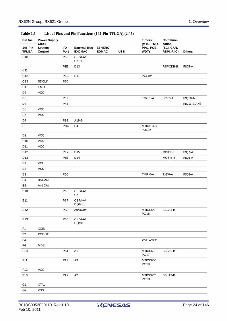
Table 1.5 List of Pins and Pin Functions (145-Pin TFLGA) (1 / 5)
Pin No. Power SupplyClockSystem Control
I/O Port
External BusEXDMAC
ETHERCEDMAC USB
Timers(MTU, TMR, PPG, POE, WDT)
Communi-cation(SCI, CAN, RSPI, RIIC) Others
145-Pin TFLGA
A1 AVSS
A2 AVCC
A3 VREFL
A4 P42 IRQ10-B/AN2
A5 P44 IRQ12/AN4
A6 P47 IRQ15-B/AN7
A7 P91 A17-B
A8 PD0 D0 POE7#
A9 PD3 D3 MTIC11V-B/POE4#
A10 PD6 D6 MTIC5V/POE1#
A11 P60 CS0#-A
A12 P62 CS2#-A/RAS#
A13 P64 CS4#-A/WE#
B1 P03 IRQ11-A/DA0
B2 P07 IRQ15-A/ADTRG0#-A
B3 VREFH
B4 P40 IRQ8-B/AN0
B5 P45 IRQ13-B/AN5
B6 P90 A16-B
B7 PD1 D1 POE6#
B8 PD5 D5 MTIC5W/POE2#
B9 VSS
B10 PE0 D8 SSLB1-B
B11 PE2 D10 POE9# SSLB3-B
B12 PE1 D9 SSLB2-B
B13 PE4 D12 SSLB0-B
C1 P01 TMCI0-A RxD6-A IRQ9-A
C2 P05 IRQ13-A/DA1
C3 VSS
C4 P41 IRQ9-B/AN1
C5 P46 IRQ14/AN6
C6 P92 A18-B
C7 PD2 D2 MTIC11W-B/POE5#
C8 PD7 D7 MTIC5U/POE0#
C9 P61 CS1#-A/SDCS#
R01DS0052EJ0110 Rev.1.10 Page 24 of 146Feb 10, 2011
RX62N Group, RX621 Group 1. Overview
C10 P63 CS3#-A/CAS#
C11PE5 D13 RSPCKB-B IRQ5-A
C12 PE3 D11 POE8#
C13 SDCLK P70
D1 EMLE
D2 VCC
D3 P02 TMCI1-A SCK6-A IRQ10-A
D4 P43 IRQ11-B/AN3
D5 VCC
D6 VSS
D7 P93 A19-B
D8 PD4 D4 MTIC11U-B/POE3#
D9 VCC
D10 VSS
D11 VCC
D12 PE7 D15 MISOB-B IRQ7-A
D13 PE6 D14 MOSIB-B IRQ6-A
E1 VCL
E2 VSS
E3 P00 TMRI0-A TxD6-A IRQ8-A
E4 BSCANP
E5 ÅiN.CÅj
E10 P65 CS5#-A/CKE
E11 P67 CS7#-A/DQM1
E12 PA0 A0/BC0# MTIOC6A/PO16
SSLA1-B
E13 P66 CS6#-A/DQM0
F1 XCIN
F2 XCOUT
F3 WDTOVF#
F4 MDE
F10 PA1 A1 MTIOC6B/PO17
SSLA2-B
F11 PA3 A3 MTIOC6D/PO19
F12 VCC
F13 PA2 A2 MTIOC6C/PO18
SSLA3-B
G1 XTAL
G2 VSS
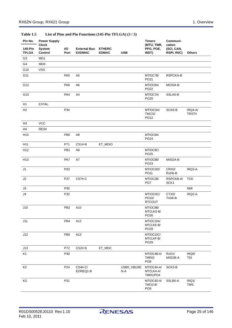
Table 1.5 List of Pins and Pin Functions (145-Pin TFLGA) (2 / 5)
Pin No. Power SupplyClockSystem Control
I/O Port
External BusEXDMAC
ETHERCEDMAC USB
Timers(MTU, TMR, PPG, POE, WDT)
Communi-cation(SCI, CAN, RSPI, RIIC) Others
145-Pin TFLGA
R01DS0052EJ0110 Rev.1.10 Page 25 of 146Feb 10, 2011
RX62N Group, RX621 Group 1. Overview
G3 MD1
G4 MD0
G10 VSS
G11 PA5 A5 MTIOC7B/PO21
RSPCKA-B
G12 PA6 A6 MTIOC8A/PO22
MOSIA-B
G13 PA4 A4 MTIOC7A/PO20
SSLA0-B
H1 EXTAL
H2 P34 MTIOC0A/TMCI3/PO12
SCK6-B IRQ4-A/TRST#
H3 VCC
H4 RES#
H10 PB0 A8 MTIOC9A/PO24
H11 P71 CS1#-B ET_MDIO
H12 PB1 A9 MTIOC9C/PO25
H13 PA7 A7 MTIOC8B/PO23
MISOA-B
J1 P33 MTIOC0D/PO11
CRX0/RxD6-B
IRQ3-A
J2 P27 CS7#-C MTIOC2B/PO7
RSPCKB-A/SCK1
TCK
J3 P35 NMI
J4 P32 MTIOC0C/PO10/RTCOUT
CTX0/TxD6-B
IRQ2-A
J10 PB2 A10 MTIOC9B/MTCLKG-B/PO26
J11 PB4 A12 MTIOC10A/MTCLKE-B/PO28
J12 PB5 A13 MTIOC10C/MTCLKF-B/PO29
J13 P72 CS2#-B ET_MDC
K1 P30 MTIOC4B-A/TMRI3/PO8
RxD1/MISOB-A
IRQ0/TDI
K2 P24 CS4#-C/ EDREQ1-B
USB0_VBUSEN-A
MTIOC4A-A/MTCLKA-A/TMRI1/PO4
SCK3-B
K3 P31 MTIOC4D-A/TMCI2-B/PO9
SSLB0-A IRQ1/TMS
Table 1.5 List of Pins and Pin Functions (145-Pin TFLGA) (3 / 5)
Pin No. Power SupplyClockSystem Control
I/O Port
External BusEXDMAC
ETHERCEDMAC USB
Timers(MTU, TMR, PPG, POE, WDT)
Communi-cation(SCI, CAN, RSPI, RIIC) Others
145-Pin TFLGA
R01DS0052EJ0110 Rev.1.10 Page 26 of 146Feb 10, 2011
RX62N Group, RX621 Group 1. Overview
K4 P26 CS6#-C MTIOC2A/TMO1/PO6
MOSIB-A/TxD1
TDO
K5 BCLK P53
K6 VSS
K7 PC7 A23/CS0#-B
ET_COL MTIC11U-A/MTCLKB-B
MISOA-A
K8 P82 EDREQ1-A ET_ETXD1/RMII_TXD1
MTIOC4A-B TRSYNC
K9 PC3 A19-A ET_TX_ER MTCLKF-A TxD5
K10 PB7 A15 MTIOC10D/PO31
K11 P73 CS3#-B ET_WOL
K12 PC0 A16-A ET_ERXD3 MTCLKG-A SSLA1-A
K13 PB3 A11 MTIOC9D/MTCLKH-B/PO27
L1 P25 CS5#-C/EDACK1-B
USB0_DPRPD MTIOC4C-A/MTCLKB-A/PO5
RxD3-B ADTRG0#-B
L2 P22 EDREQ0-B USB0_DRPD MTIOC3B-A/MTCLKC-A/TMO0/PO2
SCK0
L3 P17 MTIOC3A/PO15
TxD3-A IRQ7-B
L4 P12 TMCI1-B SCL0/RxD2-A
IRQ2-B
L5 VCC_USB
L6 P56 EDACK1-C MTIOC3C-B
L7 P52 RD# SSLB3-A/RxD2-B
L8 P83 EDACK1-A ET_CRS/RMII_CRS_DV
MTIOC4C-B TRCLK
L9 P81 EDACK0-A ET_ETXD0/RMII_TXD0
MTIOC3D-B TRDATA1
L10 P77 CS7#-B ET_RX_ER/RMII_RX_ER
L11 P75 CS5#-B ET_ERXD0/RMII_RXD0
L12 VCC
L13 PB6 A14 MTIOC10B/PO30
M1 P23 EDACK0-B USB0_DPUPE-A
MTIOC3D-A/MTCLKD-A/PO3
TxD3-B
M2 P20 USB0_ID MTIOC1A/TMRI0-B/PO0
SDA1/TxD0
M3 PLLVCC
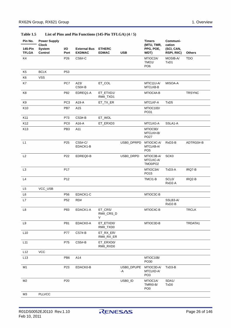
Table 1.5 List of Pins and Pin Functions (145-Pin TFLGA) (4 / 5)
Pin No. Power SupplyClockSystem Control
I/O Port
External BusEXDMAC
ETHERCEDMAC USB
Timers(MTU, TMR, PPG, POE, WDT)
Communi-cation(SCI, CAN, RSPI, RIIC) Others
145-Pin TFLGA

R01DS0052EJ0110 Rev.1.10 Page 27 of 146Feb 10, 2011
RX62N Group, RX621 Group 1. Overview
M4 P15 MTIOC0B/TMCI2-A/PO13
SCK3-A IRQ5-B
M5 P14 USB0_OVRCURA/USB0_DPUPE-B
TMRI2 IRQ4-B
M6 VSS_USB
M7 P55 WAIT#-B/EDREQ0-C
ET_EXOUT MTIOC4D-B TRDATA3
M8 P50 WR0#/WR#
SSLB1-A/TxD2-B
M9 PC6 A22/CS1#-C ET_ETXD3 MTIC11V-A/MTCLKA-B
MOSIA-A
M10 P80 EDREQ0-A ET_TX_EN/RMII_TXD_EN
MTIOC3B-B TRDATA0
M11 PC2 A18-A ET_RX_DV MTCLKE-A SSLA3-A/RxD5
M12 PC1 A17-A ET_ERXD2 MTCLKH-A SSLA2-A/SCK5
M13 VSS
N1 P21 USB0_EXICEN
MTIOC1B/TMCI0-B/PO1
SCL1/RxD0
N2 P16 USB0_VBUS/USB0_OVRCURB/USB0_VBUSEN-B
MTIOC3C-A/TMO2/PO14
RxD3-A IRQ6-B
N3 PLLVSS
N4 P13 TMO3 SDA0/TxD2-A
IRQ3-B/ADTRG1#
N5 USB0_DM
N6 USB0_DP
N7 P54 EDACK0-C ET_LINKSTA MTIOC4B-B TRDATA2
N8 P51 WR1#/BC1#/WAIT#-D
SSLB2-A/SCK2
N9 VCC
N10 PC5 A21/CS2#-C/WAIT#-C
ET_ETXD2 MTIC11W-A/MTCLKD-B
RSPCKA-A
N11 PC4 A20/CS3#-C ET_TX_CLK MTCLKC-B SSLA0-A
N12 P76 CS6#-B ET_RX_CLK/REF50CK
N13 P74 CS4#-B ET_ERXD1/RMII_RXD1
Table 1.5 List of Pins and Pin Functions (145-Pin TFLGA) (5 / 5)
Pin No. Power SupplyClockSystem Control
I/O Port
External BusEXDMAC
ETHERCEDMAC USB
Timers(MTU, TMR, PPG, POE, WDT)
Communi-cation(SCI, CAN, RSPI, RIIC) Others
145-Pin TFLGA

R01DS0052EJ0110 Rev.1.10 Page 28 of 146Feb 10, 2011
RX62N Group, RX621 Group 1. Overview
Table 1.6 List of Pins and Pin Functions (144-Pin LQFP) (1 / 5)
Pin No. Power SupplyClockSystem Control
I/O Port
External BusEXDMAC
ETHERCEDMAC USB
Timers(MTU, TMR, PPG, POE, WDT)
Communi-cation(SCI, CAN, RSPI, RIIC) Others
144-Pin LQFP
1 AVSS
2 P05 IRQ13-A/DA1
3 VCC
4 P03 IRQ11-A/DA0
5 VSS
6 P02 TMCI1-A SCK6-A IRQ10-A
7 P01 TMCI0-A RxD6-A IRQ9-A
8 P00 TMRI0-A TxD6-A IRQ8-A
9 BSCANP
10 EMLE
11 WDTOVF#
12 VSS
13 MDE
14 VCL
15 MD1
16 MD0
17 XCIN
18 XCOUT
19 RES#
20 XTAL
21 VSS
22 EXTAL
23 VCC
24 P35 NMI
25 P34 MTIOC0A/TMCI3/PO12
SCK6-B IRQ4-A/TRST#
26 P33 MTIOC0D/PO11
CRX0/RxD6-B
IRQ3-A
27 P32 MTIOC0C/PO10/RTCOUT
CTX0/TxD6-B
IRQ2-A
28 P31 MTIOC4D-A/TMCI2-B/PO9
SSLB0-A IRQ1/TMS
29 P30 MTIOC4B-A/TMRI3/PO8
RxD1/MISOB-A
IRQ0/TDI
30 P27 CS7#-C MTIOC2B/PO7
RSPCKB-A/SCK1
TCK
31 P26 CS6#-C MTIOC2A/TMO1/PO6
MOSIB-A/TxD1
TDO

R01DS0052EJ0110 Rev.1.10 Page 29 of 146Feb 10, 2011
RX62N Group, RX621 Group 1. Overview
32 P25 CS5#-C/EDACK1-B
USB0_DPRPD MTIOC4C-A/MTCLKB-A/PO5
RxD3-B ADTRG0#-B
33 P24 CS4#-C/ EDREQ1-B
USB0_VBUSEN-A
MTIOC4A-A/MTCLKA-A/TMRI1/PO4
SCK3-B
34 P23 EDACK0-B USB0_DPUPE-A
MTIOC3D-A/MTCLKD-A/PO3
TxD3-B
35 P22 EDREQ0-B USB0_DRPD MTIOC3B-A/MTCLKC-A/TMO0/PO2
SCK0
36 P21 USB0_EXICEN MTIOC1B/TMCI0-B/PO1
SCL1/RxD0
37 P20 USB0_ID MTIOC1A/TMRI0-B/PO0
SDA1/TxD0
38 P17 MTIOC3A/PO15
TxD3-A IRQ7-B
39 PLLVCC
40 P16 USB0_VBUS/USB0_OVRCURB/USB0_VBUSEN-B
MTIOC3C-A/TMO2/PO14
RxD3-A IRQ6-B
41 PLLVSS
42 P15 MTIOC0B/TMCI2-A/PO13
SCK3-A IRQ5-B
43 P14 USB0_OVRCURA/USB0_DPUPE-B
TMRI2 IRQ4-B
44 P13 TMO3 SDA0/TxD2-A
IRQ3-B/ADTRG1#
45 P12 TMCI1-B SCL0/RxD2-A
IRQ2-B
46 VCC_USB
47 USB0_DM
48 USB0_DP
49 VSS_USB
50 P56 EDACK1-C MTIOC3C-B
51 P55 WAIT#-B/EDREQ0-C
ET_EXOUT MTIOC4D-B TRDATA3
52 P54 EDACK0-C ET_LINKSTA MTIOC4B-B TRDATA2
53 BCLK P53
54 P52 RD# SSLB3-A/RxD2-B
Table 1.6 List of Pins and Pin Functions (144-Pin LQFP) (2 / 5)
Pin No. Power SupplyClockSystem Control
I/O Port
External BusEXDMAC
ETHERCEDMAC USB
Timers(MTU, TMR, PPG, POE, WDT)
Communi-cation(SCI, CAN, RSPI, RIIC) Others
144-Pin LQFP

R01DS0052EJ0110 Rev.1.10 Page 30 of 146Feb 10, 2011
RX62N Group, RX621 Group 1. Overview
55 P51 WR1#/BC1#/WAIT#-D
SSLB2-A/SCK2
56 P50 WR0#/WR#
SSLB1-A/TxD2-B
57 VSS
58 P83 EDACK1-A ET_CRS/RMII_CRS_DV
MTIOC4C-B TRCLK
59 VCC
60 PC7 A23/CS0#-B
ET_COL MTIC11U-A/MTCLKB-B
MISOA-A
61 PC6 A22/CS1#-C
ET_ETXD3 MTIC11V-A/MTCLKA-B
MOSIA-A
62 PC5 A21/CS2#-C/WAIT#-C
ET_ETXD2 MTIC11W-A/MTCLKD-B
RSPCKA-A
63 P82 EDREQ1-A ET_ETXD1/RMII_TXD1
MTIOC4A-B TRSYNC
64 P81 EDACK0-A ET_ETXD0/RMII_TXD0
MTIOC3D-B TRDATA1
65 P80 EDREQ0-A ET_TX_EN/RMII_TXD_EN
MTIOC3B-B TRDATA0
66 PC4 A20/CS3#-C ET_TX_CLK MTCLKC-B SSLA0-A
67 PC3 A19-A ET_TX_ER MTCLKF-A TxD5
68 P77 CS7#-B ET_RX_ER/RMII_RX_ER
69 P76 CS6#-B ET_RX_CLK/REF50CK
70 PC2 A18-A ET_RX_DV MTCLKE-A SSLA3-A/RxD5
71 P75 CS5#-B ET_ERXD0/RMII_RXD0
72 P74 CS4#-B ET_ERXD1/RMII_RXD1
73 PC1 A17-A ET_ERXD2 MTCLKH-A SSLA2-A/SCK5
74 VCC
75 PC0 A16-A ET_ERXD3 MTCLKG-A SSLA1-A
76 VSS
77 P73 CS3#-B ET_WOL
78 PB7 A15 MTIOC10D/PO31
79 PB6 A14 MTIOC10B/PO30
80 PB5 A13 MTIOC10C/MTCLKF-B/PO29
81 PB4 A12 MTIOC10A/MTCLKE-B/PO28
Table 1.6 List of Pins and Pin Functions (144-Pin LQFP) (3 / 5)
Pin No. Power SupplyClockSystem Control
I/O Port
External BusEXDMAC
ETHERCEDMAC USB
Timers(MTU, TMR, PPG, POE, WDT)
Communi-cation(SCI, CAN, RSPI, RIIC) Others
144-Pin LQFP

R01DS0052EJ0110 Rev.1.10 Page 31 of 146Feb 10, 2011
RX62N Group, RX621 Group 1. Overview
82 PB3 A11 MTIOC9D/MTCLKH-B/PO27
83 PB2 A10 MTIOC9B/MTCLKG-B/PO26
84 PB1 A9 MTIOC9C/PO25
85 P72 CS2#-B ET_MDC
86 P71 CS1#-B ET_MDIO
87 PB0 A8 MTIOC9A/PO24
88 PA7 A7 MTIOC8B/PO23
MISOA-B
89 PA6 A6 MTIOC8A/PO22
MOSIA-B
90 PA5 A5 MTIOC7B/PO21
RSPCKA-B
91 VCC
92 PA4 A4 MTIOC7A/PO20
SSLA0-B
93 VSS
94 PA3 A3 MTIOC6D/PO19
95 PA2 A2 MTIOC6C/PO18
SSLA3-B
96 PA1 A1 MTIOC6B/PO17
SSLA2-B
97 PA0 A0/BC0#/ MTIOC6A/PO16
SSLA1-B
98 P67 CS7#-A/DQM1
99 P66 CS6#-A/DQM0
100 P65 CS5#-A/CKE
101 PE7 D15 MISOB-B IRQ7-A
102 PE6 D14 MOSIB-B IRQ6-A
103 VCC
104 SDCLK P70
105 VSS
106 PE5 D13 RSPCKB-B IRQ5-A
107 PE4 D12 SSLB0-B
108 PE3 D11 POE8#
109 PE2 D10 POE9# SSLB3-B
110 PE1 D9 SSLB2-B
111 PE0 D8 SSLB1-B
Table 1.6 List of Pins and Pin Functions (144-Pin LQFP) (4 / 5)
Pin No. Power SupplyClockSystem Control
I/O Port
External BusEXDMAC
ETHERCEDMAC USB
Timers(MTU, TMR, PPG, POE, WDT)
Communi-cation(SCI, CAN, RSPI, RIIC) Others
144-Pin LQFP

R01DS0052EJ0110 Rev.1.10 Page 32 of 146Feb 10, 2011
RX62N Group, RX621 Group 1. Overview
112 P64 CS4#-A/WE#
113 P63 CS3#-A/CAS#
114 P62 CS2#-A/RAS#
115 P61 CS1#-A/SDCS#
116 VSS
117 P60 CS0#-A
118 VCC
119 PD7 D7 MTIC5U/POE0#
120 PD6 D6 MTIC5V/POE1#
121 PD5 D5 MTIC5W/POE2#
122 PD4 D4 MTIC11U-B/POE3#
123 PD3 D3 MTIC11V-B/POE4#
124 PD2 D2 MTIC11W-B/POE5#
125 PD1 D1 POE6#
126 PD0 D0 POE7#
127 P93 A19-B
128 P92 A18-B
129 P91 A17-B
130 VSS
131 P90 A16-B
132 VCC
133 P47 IRQ15-B/AN7
134 P46 IRQ14/AN6
135 P45 IRQ13-B/AN5
136 P44 IRQ12/AN4
137 P43 IRQ11-B/AN3
138 P42 IRQ10-B/AN2
139 P41 IRQ9-B/AN1
140 VREFL
141 P40 IRQ8-B/AN0
142 VREFH
143 AVCC
144 P07 IRQ15-A/ADTRG0#-A
Table 1.6 List of Pins and Pin Functions (144-Pin LQFP) (5 / 5)
Pin No. Power SupplyClockSystem Control
I/O Port
External BusEXDMAC
ETHERCEDMAC USB
Timers(MTU, TMR, PPG, POE, WDT)
Communi-cation(SCI, CAN, RSPI, RIIC) Others
144-Pin LQFP

R01DS0052EJ0110 Rev.1.10 Page 33 of 146Feb 10, 2011
RX62N Group, RX621 Group 1. Overview
Table 1.7 List of Pins and Pin Functions (100-Pin LQFP) (1 / 4)
Pin No. Power SupplyClockSystem Control
I/O Port External Bus
ETHERCEDMAC USB
Timers(MTU, TMR, PPG, POE)
Communi-cation(SCI, CAN, RSPI, RIIC) Others
100-PIn LQFP
1 VCC
2 EMLE
3 VSS
4 MDE
5 VCL
6 MD1
7 MD0
8 XCIN
9 XCOUT
10 RES#
11 XTAL
12 VSS
13 EXTAL
14 VCC
15 P35 NMI
16 P34 MTIOC0A/TMCI3/PO12
SCK6 IRQ4-A/TRST#
17 P33 MTIOC0D/PO11
CRX0/RxD6
IRQ3-A
18 P32 MTIOC0C/PO10/RTCOUT
CTX0/TxD6
IRQ2-A
19 P31 MTIOC4D-A/TMCI2/PO9
SSLB0-A IRQ1/TMS
20 P30 MTIOC4B-A/TMRI3/PO8
RxD1/MISOB-A
IRQ0/TDI
21 P27 CS7# MTIOC2B/PO7
RSPCKB-A/SCK1
TCK
22 P26 CS6# MTIOC2A/TMO1/PO6
MOSIB-A/TxD1
TDO
23 P25 CS5# USB0_DPRPD MTIOC4C/MTCLKB-A/PO5
RxD3 ADTRG0#-B
24 P24 CS4#/ USB0_VBUSEN-A
MTIOC4A/MTCLKA/TMRI1/PO4
SCK3
25 P23 USB0_DPUPE-A
MTIOC3D/MTCLKD-A/PO3
TxD3
26 P22 USB0_DRPD MTIOC3B/MTCLKC-A/TMO0/PO2
SCK0

R01DS0052EJ0110 Rev.1.10 Page 34 of 146Feb 10, 2011
RX62N Group, RX621 Group 1. Overview
27 P21 USB0_EXICEN MTIOC1B/TMCI0/PO1
RxD0
28 P20 USB0_ID MTIOC1A/TMRI0/PO0
TxD0
29 PLLVCC
30 P16 USB0_VBUS/USB0_OVRCURB/USB0_VBUSEN-B
MTIOC3C/TMO2/PO14
IRQ6-B
31 PLLVSS
32 P14 USB0_OVRCURA/USB0_DPUPE-B
MTIOC3A/TMRI2/PO15
IRQ4-B
33 P13 MTIOC0B/TMO3/PO13
SDA0/TxD2-A
IRQ3-B/ADTRG1#
34 P12 TMCI1 SCL0/RxD2-A
IRQ2-B
35 VCC_USB
36 USB0_DM
37 USB0_DP
38 VSS_USB
39 P55 WAIT#-B MTIOC4D-B
40 P54 MTIOC4B-B
41 BCLK P53
42 P52 RD# SSLB3-A/RxD2-B
43 P51 WR1#/BC1#/WAIT#-D
SSLB2-A/SCK2
44 P50 WR0#/WR#
SSLB1-A/TxD2-B
45 PC7 A23/CS0#
ET_COL MTIC11U-A/MTCLKB-B
MISOA-A
46 PC6 A22/CS1#
ET_ETXD3 MTIC11V-A/MTCLKA-B
MOSIA-A
47 PC5 A21/CS2#/WAIT#-C
ET_ETXD2 MTIC11W-A/MTCLKD-B
RSPCKA-A
48 PC4 A20/CS3# ET_TX_CLK MTCLKC-B SSLA0-A
49 PC3 A19 ET_TX_ER MTCLKF-A TxD5
50 PC2 A18 ET_RX_DV MTCLKE-A SSLA3-A/RxD5
51 PC1 A17 ET_ERXD2 MTCLKH-A SSLA2-A/SCK5
52 PC0 A16 ET_ERXD3 MTCLKG-A SSLA1-A
Table 1.7 List of Pins and Pin Functions (100-Pin LQFP) (2 / 4)
Pin No. Power SupplyClockSystem Control
I/O Port External Bus
ETHERCEDMAC USB
Timers(MTU, TMR, PPG, POE)
Communi-cation(SCI, CAN, RSPI, RIIC) Others
100-PIn LQFP

R01DS0052EJ0110 Rev.1.10 Page 35 of 146Feb 10, 2011
RX62N Group, RX621 Group 1. Overview
53 PB7 A15 ET_CRS/RMII_CRS_DV
MTIOC10D/PO31
54 PB6 A14 ET_ETXD1/RMII_TXD1
MTIOC10B/PO30
55 PB5 A13 ET_ETXD0/RMII_TXD0
MTIOC10C/MTCLKF-B/PO29
56 PB4 A12 ET_TX_EN/RMII_TXD_EN
MTIOC10A/MTCLKE-B/PO28
57 PB3 A11 ET_RX_ER/RMII_RX_ER
MTIOC9D/MTCLKH-B/PO27
58 PB2 A10 ET_RX_CLK/REF50CK
MTIOC9B/MTCLKG-B/PO26
59 PB1 A9 ET_ERXD0/RMII_RXD0
MTIOC9C/PO25
60 VCC
61 PB0 A8 ET_ERXD1/RMII_RXD1
MTIOC9A/PO24
62 VSS
63 PA7 A7 ET_WOL MTIOC8B/PO23
MISOA-B
64 PA6 A6 ET_EXOUT MTIOC8A/PO22
MOSIA-B
65 PA5 A5 ET_LINKSTA MTIOC7B/PO21
RSPCKA-B
66 PA4 A4 ET_MDC MTIOC7A/PO20
SSLA0-B
67 PA3 A3 ET_MDIO MTIOC6D/PO19
68 PA2 A2 MTIOC6C/PO18
SSLA3-B
69 PA1 A1 MTIOC6B/PO17
SSLA2-B
70 PA0 A0/BC0# MTIOC6A/PO16
SSLA1-B
71 PE7 D15 MISOB-B IRQ7
72 PE6 D14 MOSIB-B IRQ6-A
73 PE5 D13 RSPCKB-B IRQ5
74 PE4 D12 SSLB0-B
75 PE3 D11 POE8#
76 PE2 D10 POE9# SSLB3-B
77 PE1 D9 SSLB2-B
78 PE0 D8 SSLB1-B
79 PD7 D7 MTIC5U/POE0#
Table 1.7 List of Pins and Pin Functions (100-Pin LQFP) (3 / 4)
Pin No. Power SupplyClockSystem Control
I/O Port External Bus
ETHERCEDMAC USB
Timers(MTU, TMR, PPG, POE)
Communi-cation(SCI, CAN, RSPI, RIIC) Others
100-PIn LQFP
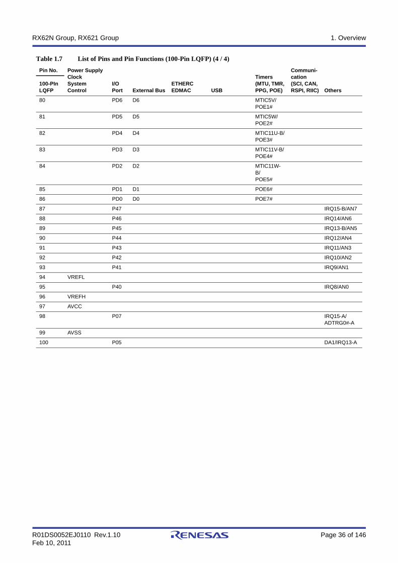
R01DS0052EJ0110 Rev.1.10 Page 36 of 146Feb 10, 2011
RX62N Group, RX621 Group 1. Overview
80 PD6 D6 MTIC5V/POE1#
81 PD5 D5 MTIC5W/POE2#
82 PD4 D4 MTIC11U-B/POE3#
83 PD3 D3 MTIC11V-B/POE4#
84 PD2 D2 MTIC11W-B/POE5#
85 PD1 D1 POE6#
86 PD0 D0 POE7#
87 P47 IRQ15-B/AN7
88 P46 IRQ14/AN6
89 P45 IRQ13-B/AN5
90 P44 IRQ12/AN4
91 P43 IRQ11/AN3
92 P42 IRQ10/AN2
93 P41 IRQ9/AN1
94 VREFL
95 P40 IRQ8/AN0
96 VREFH
97 AVCC
98 P07 IRQ15-A/ADTRG0#-A
99 AVSS
100 P05 DA1/IRQ13-A
Table 1.7 List of Pins and Pin Functions (100-Pin LQFP) (4 / 4)
Pin No. Power SupplyClockSystem Control
I/O Port External Bus
ETHERCEDMAC USB
Timers(MTU, TMR, PPG, POE)
Communi-cation(SCI, CAN, RSPI, RIIC) Others
100-PIn LQFP

R01DS0052EJ0110 Rev.1.10 Page 37 of 146Feb 10, 2011
RX62N Group, RX621 Group 1. Overview
Table 1.8 List of Pins and Pin Functions (85-Pin TFLGA) (1 / 3)
Pin No. Power SupplyClockSystem Control I/O Port
External Bus USB
Timers(MTU, TMR, PPG)
Communi-cation(SCI, CAN, RSPI, RIIC) Others
85-Pin TFLGA
A1 P05 DA1/IRQ13-A
A2 AVCC
A3 VREFL
A4 P43 IRQ11-B/AN3
A5 P47 IRQ15/AN7
A6 PD1 D1
A7 PD4 D4 MTIC11U
A8 PD5 D5 MTIC5W
A9 PD7 D7 MTIC5U
A10 PD6 D6 MTIC5V
B1 VCC
B2 AVSS
B3 VREFH
B4 P42 IRQ10/AN2
B5 P46 IRQ14/AN6
B6 PD0 D0
B7 PD2 D2 MTIC11W
B8 PD3 D3 MTIC11V
B9 PA3 A3 MTIOC6D/PO19
B10 PA1 A1 MTIOC6B/PO17 SSLA2
C1 P03 IRQ11-A/DA0
C2 VSS
C3 P40 IRQ8/AN0
C4 P41 IRQ9/AN1
C5 P44 IRQ12/AN4
C6 P45 IRQ13-B/AN5
C7 MD1
C8 BSCANP
C9 PA5 A5 MTIOC7B/PO21 RSPCKA
C10 PA0 A0 MTIOC6A/PO16 SSLA1
D1 MDE
D2 EMLE
D3 MD0
D4 RES#

R01DS0052EJ0110 Rev.1.10 Page 38 of 146Feb 10, 2011
RX62N Group, RX621 Group 1. Overview
D8 VCL
D9 PA6 A6 MTIOC8A/PO22 MOSIA
D10 PA2 A2 MTIOC6C/PO18 SSLA3
E1 XCIN
E2 XCOUT
E3 P34 MTIOC0A/TMCI3/PO12 SCK6 IRQ4-A/TRST#
E8 VSS
E9 PB0 A8 MTIOC9A/PO24
E10 PA4 A4 MTIOC7A/PO20 SSLA0
F1 XTAL
F2 EXTAL
F3 P32 MTIOC0C/PO10/RTCOUT TxD6/CTX0 IRQ2-A
F8 VCC
F9 PB2 A10 MTIOC9B/MTCLKG-B/PO26
F10 PA7 A7 MTIOC8B/PO23 MISOA
G1 P35 NMI
G2 P33 MTIOC0D/PO11 RxD6/CRX0 IRQ3-A
G3 P27 CS7# MTIOC2B/PO7 SCK1/RSPCKB TCK
G8 PB3 A11 MTIOC9D/MTCLKH-B/PO27
G9 PB5 A13 MTIOC10C/MTCLKF-B/PO29
G10 PB1 A9 MTIOC9C/PO25
H1 P31 MTIOC4D/TMCI2/PO9 SSLB0 IRQ1/TMS
H2 P30 MTIOC4B/TMRI3/PO8 RxD1/MISOB IRQ0/TDI
H3 P26 CS6# MTIOC2A/TMO1/PO6 TxD1/MOSIB TDO
H4 PLLVCC
H5 P14 USB0_OVRCURA/USB0_DPUPE-B
MTIOC3A/TMRI2/PO15 IRQ4-B
H6 P13 MTIOC0B/TMO3/PO13 TxD2-A/SDA0 IRQ3-B/ADTRG1#
H7 BCLK P53
H8 PB6 A14 MTIOC10B/PO30
H9 PB7 A15 MTIOC10D/PO31
H10 PB4 A12 MTIOC10A/MTCLKE-B/PO28
J1 P25 CS5# USB0_DPRPD MTIOC4C/MTCLKB/PO5 RxD3 ADTRG0#
J2 P23 USB0_DPUPE-A MTIOC3D/MTCLKD/PO3 TxD3
J3 P24 CS4# USB0_VBUSEN-A
MTIOC4A/MTCLKA-A/TMRI1/PO4
SCK3
Table 1.8 List of Pins and Pin Functions (85-Pin TFLGA) (2 / 3)
Pin No. Power SupplyClockSystem Control I/O Port
External Bus USB
Timers(MTU, TMR, PPG)
Communi-cation(SCI, CAN, RSPI, RIIC) Others
85-Pin TFLGA

R01DS0052EJ0110 Rev.1.10 Page 39 of 146Feb 10, 2011
RX62N Group, RX621 Group 1. Overview
J4 P16 USB0_VBUS/USB0_OVRCURB/USB0_VBUSEN-B
MTIOC3C/TMO2/PO14 IRQ6
J5 VCC_USB
J6 USB0_DM
J7 P52 RD# RxD2-B/SSLB3
J8 P51 WAIT# SCK2/SSLB2
J9 PC3 A19 MTCLKF-A TxD5
J10 PC0 A16 MTCLKG-A
K1 P21 USB0_EXICEN MTIOC1B/TMCI0/PO1 RxD0/SCL1
K2 P22 USB0_DRPD MTIOC3B/MTCLKC/TMO0/PO2 SCK0
K3 P20 USB0_ID MTIOC1A/TMRI0/PO0 TxD0/SDA1
K4 PLLVSS
K5 P12 TMCI1 RxD2-A/SCL0 IRQ2-B
K6 USB0_DP
K7 VSS_USB
K8 P50 WR0# TxD2-B/SSLB1
K9 PC2 A18 MTCLKE-A RxD5
K10 PC1 A17 MTCLKH-A SCK5
Table 1.8 List of Pins and Pin Functions (85-Pin TFLGA) (3 / 3)
Pin No. Power SupplyClockSystem Control I/O Port
External Bus USB
Timers(MTU, TMR, PPG)
Communi-cation(SCI, CAN, RSPI, RIIC) Others
85-Pin TFLGA

R01DS0052EJ0110 Rev.1.10 Page 40 of 146Feb 10, 2011
RX62N Group, RX621 Group 1. Overview
1.5 Pin Functions
Table 1.8 lists the pin functions.
Table 1.9 Pin Functions (1 / 7)
Classifications Pin Name I/O Description
Power supply VCC Input Power supply pin. Connect it to the system power supply.
VCL Input Connect this pin to VSS via a 0.1-F capacitor. The capacitor should be placed close to the pin.
VSS Input Ground pin. Connect it to the system power supply (0 V).
PLLVCC Input Power supply pin for the PLL circuit. Connect it to the system power supply.
PLLVSS Input Ground pin for the PLL circuit.
Clock XTAL Output Pins for a crystal resonator. An external clock signal can be input through the EXTAL pin.
EXTAL Input
BCLK Output Outputs the external bus clock for external devices.
SDCLK Output Outputs the clock dedicated for the SDRAM.
XCOUT Output Input/output pins for the subclock generation circuit. Connect a crystal resonator between XCOUT and XCIN.
XCIN Input
Operating mode control MD0, MD1, MDE Input Pins for setting the operating mode. The signal levels on these pins must not be changed during operation.
System control RES# Input Reset signal input pin. This LSI enters the reset state when this signal goes low.
EMLE Input Input pin to enable the connection of the on-chip emulator signal. When the on-chip emulator is used, this pin should be driven high. When not used, it should be driven low.
BSCANP Input Boundary scan pin. Boundary scan is enabled when this pin goes high. When not used, it should be driven low.
CNVSS CNVSS Input Connect this pin to VSS via pull-down resister.
On-chip emulator TRST# Input On-chip emulator pins or boundary scan pins. When the EMLE pin is driven high, these pins are dedicated for the on-chip emulator.
TMS Input
TDI Input
TCK Input
TDO Output
TRCLK Output This pin outputs the clock for synchronization with the trace data.
TRSYNC Output This pin indicates that output from the TRDATA0 to TRDATA3 pins is valid.
TRDATA0-A/TRDATA3-B Output These pins output the trace information.
Address bus A0 to A15A16-A/A16-B to A23-A/A23-B
Output Output pins for the address.
Data bus D0 to D31 I/O Input and output pins for the bidirectional data bus.

R01DS0052EJ0110 Rev.1.10 Page 41 of 146Feb 10, 2011
RX62N Group, RX621 Group 1. Overview
Bus control RD# Output Strobe signal which indicates that reading from the external bus interface space is in progress.
WR# Output Strobe signal which indicates that writing to the external bus interface space is in progress, in 1-write strobe mode.
WR0# to WR3# Output Strobe signals which indicate that any group of data bus pins (D7 to D0, D15 to D8, D23 to D16, and D31 to D24) is valid in writing to the external bus interface space, in byte strobe mode.
BC0# to BC3# Output Strobe signals which indicate that any group of data bus pins (D7 to D0, D15 to D8, D23 to D16, and D31 to D24) is valid in access to the external bus interface space, in 1-write strobe mode.
WE# Output Output pin for SDRAM write enable signals.
CAS# Output Output pin for SDRAM column address strobe signals.
RAS# Output Output pin for SDRAM row address strobe signals.
CKE Output Output pin for SDRAM clock enable signals.
DQM0 to DQM34 Output Output pins for SDRAM I/O data mask enable signals.
SDCS# Output Output pin for SDRAM chip select signals.
CS0#-A/CS0#-BCS1#-A/CS1#-B/CS1#-CCS2#-A/CS2#-B/CS2#-CCS3#-A/CS3#-B/CS3#-CCS4#-A/CS4#-B/CS4#-CCS5#-A/CS5#-B/CS5#-CCS6#-A/CS6#-B/CS6#-CCS7#-A/CS7#-B/CS7#-C
Output Select signals for areas 0 to 7.
WAIT#-A/WAIT#-B/WAIT#-C/WAIT#-D
Input Input pins for wait request signals in access to the external space.
EXDMA controller EDREQ0-A/EDREQ0-B/EDREQ0-C
Input Input pins for external requests of channel 0.
EDREQ1-A/EDREQ1-B/EDREQ1-C
Input Input pins for external requests of channel 1.
EDACK0-A/EDACK0-B/EDACK0-C
Output Output pins for single address transfer acknowledge signals of channel 0.
EDACK1-A/EDACK1-B/EDACK1-C
Output Output pins for single address transfer acknowledge signals of channel 1.
Interrupt NMI Input Non-maskable interrupt request signal.
IRQ0-A/IRQ0-BIRQ1-A/IRQ1-BIRQ2-A/IRQ2-BIRQ3-A/IRQ3-BIRQ4-A/IRQ4-BIRQ5-A/IRQ5-BIRQ6-A/IRQ6-BIRQ7-A/IRQ7-BIRQ8-A/IRQ8-BIRQ9-A/IRQ9-BIRQ10-A/IRQ10-BIRQ11-A/IRQ11-BIRQ12IRQ13-A/IRQ13-BIRQ14IRQ15-A/IRQ15-B
Input Interrupt request signals.
Table 1.9 Pin Functions (2 / 7)
Classifications Pin Name I/O Description

R01DS0052EJ0110 Rev.1.10 Page 42 of 146Feb 10, 2011
RX62N Group, RX621 Group 1. Overview
Multi-function timer pulse unit
MTIOC0AMTIOC0B MTIOC0CMTIOC0D
I/O The TGRA0 to TGRD0 input capture input/output compare output/PWM output pins.
MTIOC1AMTIOC1B
I/O The TGRA1 and TGRB1 input capture input/output compare output/PWM output pins.
MTIOC2AMTIOC2B
I/O The TGRA2 and TGRB2 input capture input/output compare output/PWM output pins.
MTIOC3A MTIOC3B-A/MTIOC3B-BMTIOC3C-A/MTIOC3C-BMTIOC3D-A/MTIOC3D-B
I/O The TGRA3 to TGRD3 input capture input/output compare output/PWM output pins.
MTIOC4A-A/MTIOC4A-BMTIOC4B-A/MTIOC4B-BMTIOC4C-A/MTIOC4C-BMTIOC4D-A/MTIOC4D-B
I/O The TGRA4 and TGRB4 input capture input/output compare output/PWM output pins.
MTIC5U-A/MTIC5U-BMTIC5V-A/MTIC5V-BMTIC5W-A/MTIC5W-B
Input The TGRU5, TGRV5, and TGRW5 input capture input/dead time compensation input pins.
MTIOC6AMTIOC6BMTIOC6CMTIOC6D
I/O The TGRA6 to TGRD6 input capture input/output compare output/PWM output pins.
MTIOC7AMTIOC7B
I/O The TGRA7 and TGRB7 input capture input/output compare output/PWM output pins.
MTIOC8AMTIOC8B
I/O The TGRA8 and TGRB8 input capture input/output compare output/PWM output pins.
MTIOC9AMTIOC9BMTIOC9CMTIOC9D
I/O The TGRA9 to TGRD9 input capture input/output compare output/PWM output pins.
MTIOC10AMTIOC10BMTIOC10CMTIOC10D
I/O The TGRA10 to TGRB10 input capture input/output compare output/PWM output pins.
MTIC11U-A/MTIC11U-BMTIC11V-A/MTIC11V-BMTIC11W-A/MTIC11W-B
Input The TGRU11, TGRV11, and TGRW11 input capture input/dead time compensation input pins.
MTCLKA-A/MTCLKA-BMTCLKB-A/MTCLKB-BMTCLKC-A/MTCLKC-BMTCLKD-A/MTCLKD-BMTCLKE-A/MTCLKE-BMTCLKF-A/MTCLKF-BMTCLKG-A/MTCLKG-BMTCLKH-A/MTCLKH-B
Input Input pins for external clock signals.
Port output enable POE0# to POE9# Input Input pins for request signals to place the MTU large-current pin in the high impedance state.
Programmable pulse generator
PO0 to PO31 Output Output pins for the pulse signals.
Table 1.9 Pin Functions (3 / 7)
Classifications Pin Name I/O Description

R01DS0052EJ0110 Rev.1.10 Page 43 of 146Feb 10, 2011
RX62N Group, RX621 Group 1. Overview
8-bit timer TMO0 to TMO3 Output Output pins for the compare match signals.
TMCI0-A/TMCI0-BTMCI1-A/TMCI1-BTMCI2-A/TMCI2-BTMCI3-A/TMCI3-B
Input Input pins for the external clock signals that drive for the counters.
TMRI0-A/TMRI0-BTMRI1TMRI2TMRI3-A/TMRI3-B
Input Input pins for the counter-reset signals.
Watchdog timer WDTOVF# Output Output pin for the counter-overflow signal in watchdog-timer mode.
Serial communications interface
TxD0TxD1-A/TxD1-BTxD2-A/TxD2-BTxD3-A/TxD3-BTxD5TxD6-A/TxD6-B
Output Output pins for data transmission.
RxD0RxD1-A/RxD1-BRxD2-A/RxD2-BRxD3-A/RxD3-BRxD5RxD6-A/RxD6-B
Input Input pins for data reception.
SCK0SCK1-A/SCK1-BSCK2-A/SCK2-BSCK3-A/SCK3-BSCK5SCK6-A/SCK6-B
I/O Input/output pins for clock signals.
I2C bus interface SCL0, SCL1 I/O Input/output pins for I2C bus interface clocks. Bus can be directly driven by the NMOS open drain output.
SDA0, SDA1 I/O Input/output pins for I2C bus interface data. Bus can be directly driven by the NMOS open drain output.
Table 1.9 Pin Functions (4 / 7)
Classifications Pin Name I/O Description

R01DS0052EJ0110 Rev.1.10 Page 44 of 146Feb 10, 2011
RX62N Group, RX621 Group 1. Overview
Ethernet controller REF50CK Input 50-MHz reference clock. This pin inputs reference signals for transmission/reception timings in RMII mode.
RMII_CRS_DV Input Indicates that there are carrier detection signals and valid receive data on RMII_RXD1 and RMII_RXD0 in RMII mode.
RMII_TXD0, RMII_TXD1 Output 2-bit transmit data in RMII mode.
RMII_RXD0, RMII_RXD1 Input 2-bit receive data in RMII mode.
RMII_TXD_EN Output Output pin for data transmit enable signals in RMII mode.
RMII_RX_ER Input Indicates an error has occurred during reception of data in RMII mode.
ET_CRS Input Carrier detection/data reception enable pin.
ET_RX_DV Input Indicates that there are valid receive data on ET_ERXD3 to ET_ERXD0.
ET_EXOUT Output General-purpose external output pin.
ET_LINKSTA Input Inputs link status from the PHY-LSI.
ET_ETXD0 to ET_ETXD3 Output 4 bits of MII transmit data.
ET_ERXD0 to ET_ERXD3 Input 4 bits of MII receive data.
ET_TX_EN Output Transmit enable pin. Indicates that transmit data is ready on ET_ETXD3 to ET_ETXD0.
ET_TX_ER Output Transmit error pin. Notifies the PHY_LSI of an error during transmission.
ET_RX_ER Input Receive error pin. Recognizes an error during reception.
ET_TX_CLK Input Transmit clock pin. This pin inputs reference signals for output timings from ET_TX_EN, ET_ETXD3 to ET_ETXD0, and ET_TX_ER.
ET_RX_CLK Input Receive clock pin. This pin inputs reference signals for input timings to ET_RX_DV, ET_ERXD3 to ET_ERXD0, and ET_RX_ER.
ET_COL Input Inputs collision detection signals.
ET_WOL Output Receives Magic packets.
ET_MDC Output Outputs reference clock signals for information transfer via ET_MDIO.
ET_MDIO I/O Inputs or outputs bidirectional signals for exchange of management information between the RX62N/RX621 Group and the PHY-LSI.
Table 1.9 Pin Functions (5 / 7)
Classifications Pin Name I/O Description

R01DS0052EJ0110 Rev.1.10 Page 45 of 146Feb 10, 2011
RX62N Group, RX621 Group 1. Overview
USB 2.0 host/function module
VCC_USB Input Power-supply pin for the USB. Connect this pin to the system power supply even when the USB is not to be used.
VSS_USB Input Ground pin for the USB. Connect this pin to the system power supply (0 V) even when the USB is not to be used.
USB0_DPUSB1_DP
I/O Inputs or outputs D+ data for the USB bus.
USB0_DMUSB1_DM
I/O Inputs or outputs D- data for the USB bus.
USB0_DPRPDUSB1_DPRPD
Output Enable D+ pull-down.
USB0_DRPDUSB1_DRPD
Output Enable D- pull-down.
USB0_EXICENUSB1_EXICEN
Output Connect these pins to the OTG power supply IC.
USB0_IDUSB1_ID
Input Connect these pins to the OTG power supply IC.
USB0_VBUSEN-A/USB0_VBUSEN-BUSB1_VBUSEN-A/USB1_VBUSEN-B
Output VBUS power enable pins for the USB.
USB0_DPUPE-A/USB0_DPUPE-BUSB1_DPUPE-A/USB1_DPUPE-B
Output Pull-up pins for the USB.
USB0_OVRCURA/USB0_OVRCURBUSB1_OVRCURA/USB1_OVRCURB
Input Over current pins for the USB.
USB0_VBUSUSB1_VBUS
Input Input pins for detection of connection and disconnection of the USB cable.
CAN module CRX0 Input Input pins for the CAN.
CTX0 Output Output pins for the CAN.
Serial peripheral interfaces
RSPCKA-A/RSPCKA-B
I/O Clock input/output pins for the RSPI.
RSPCKB-A/RSPCKB-B
I/O Clock input/output pins for the RSPI
MOSIA-A/MOSIA-BMOSIB-A/MOSIB-B
I/O Input or output data output from the master for the RSPI.
MISOA-A/MISOA-BMISOB-A/MISOB-B
I/O Input or output data output from the slave for the RSPI.
SSLA0-A/SSLA0-B I/O Select the slave for the RSPI.
SSLA1-A/SSLA1-BSSLA2-A/SSLA2-BSSLA3-A/SSLA3-B
Output
SSLB0-A/SSLB0-B I/O
SSLB1-A/SSLB1-BSSLB2-A/SSLB2-BSSLB3-A/SSLB3-B
Output
Realtime clock RTCOUT Output Output pin for 1-Hz clock.
A/D converter AN0 to AN7 Input Input pins for the analog signals to be processed by the A/D converter.
ADTRG0#-A/ADTRG0#-BADTRG1#
Input Input pins for the external trigger signals that start the A/D conversion.
D/A converter DA0, DA1 Output Output pins for the analog signals from the D/A converter.
Table 1.9 Pin Functions (6 / 7)
Classifications Pin Name I/O Description
R01DS0052EJ0110 Rev.1.10 Page 46 of 146Feb 10, 2011
RX62N Group, RX621 Group 1. Overview
Analog power supply AVCC Input Analog power supply pin for the A/D and D/A converters. When the A/D and D/A converters are not in use, connect this pin to the system power supply.
AVSS Input Ground pin for the A/D and D/A converters. Connect this pin to the system power supply (0 V).
VREFH Input Reference power supply pin for the A/D and D/A converters. When the A/D and D/A converters are not in use, connect this pin to the system power supply.
VREFL Input Reference ground pin for the A/D and D/A converters. Make sure to connect this pin to the analog reference power supply (0 V). When the A/D and D/A converters are not in use, connect this pin to the system power supply (0 V). For details, see section 34.6.7, Ranges of Settings for Analog Power Supply and Other Pins.
I/O ports P00 to P03, P05, P07 I/O 6-bit input/output pins.
P10 to P17 I/O 8-bit input/output pins.
P20 to P27 I/O 8-bit input/output pins.
P30 to P34 I/O 5-bit input/output pins.
P35 Input 1-bit input pin.
P40 to P47 I/O 8-bit input/output pins.
P50 to P52, P54 to P57 I/O 7-bit input/output pins.
P53 Input 1-bit input pin.
P60 to P67 I/O 8-bit input/output pins.
P70 to P77 I/O 8-bit input/output pins.
P80 to P85 I/O 6-bit input/output pins.
P90 to P97 I/O 8-bit input/output pins.
PA0 to PA7 I/O 8-bit input/output pins.
PB0 to PB7 I/O 8-bit input/output pins.
PC0 to PC7 I/O 8-bit input/output pins.
PD0 to PD7 I/O 8-bit input/output pins.
PE0 to PE7 I/O 8-bit input/output pins.
PF0 to PF4 I/O 5-bit input/output pins.
PG0 to PG7 I/O 8-bit input/output pins.
Table 1.9 Pin Functions (7 / 7)
Classifications Pin Name I/O Description

R01DS0052EJ0110 Rev.1.10 Page 47 of 146Feb 10, 2011
RX62N Group, RX621 Group 2. CPU
2. CPUThe RX CPU has sixteen general-purpose registers, nine control registers, and one accumulator used for DSP
instructions.
Figure 2.1 Register Set of the CPU
Note: * The stack pointer (SP) can be the interrupt stack pointer (ISP) or user stack pointer (USP), according to the value of the U bit in the PSW.
USP (User stack pointer)
ISP (Interrupt stack pointer)
INTB (Interrupt table register)
PC (Program counter)
PSW (Processor status word)
BPC (Backup PC)
BPSW (Backup PSW)
FINTV (Fast interrupt vector register)
FPSW (Floating-point status word)
R15
R14
R13
R12
R11
R10
R9
R8
R7
R6
R5
R4
R3
R2
R1
R0 (SP) *
General-purpose register
Control register
b31 b0
b31 b0
DSP instruction register
b63 b0b15b16
ACC (Accumulator)
R01DS0052EJ0110 Rev.1.10 Page 48 of 146Feb 10, 2011
RX62N Group, RX621 Group 2. CPU
2.1 General-Purpose Registers (R0 to R15)
This CPU has sixteen general-purpose registers (R0 to R15). R1 to R15 can be used as data registers or address registers.
R0, a general-purpose register, also functions as the stack pointer (SP). The stack pointer is switched to operate as the
interrupt stack pointer (ISP) or user stack pointer (USP) by the value of the stack pointer select bit (U) in the processor
status word (PSW).
2.2 Control Registers
(1) Interrupt Stack Pointer (ISP)/User Stack Pointer (USP)
The stack pointer (SP) can be either of two types, the interrupt stack pointer (ISP) or the user stack pointer (USP).
Whether the stack pointer operates as the ISP or USP depends on the value of the stack pointer select bit (U) in the
processor status word (PSW).
Set the ISP or USP to a multiple of four, as this reduces the numbers of cycles required to execute interrupt sequences
and instructions entailing stack manipulation.
(2) Interrupt Table Register (INTB)
The interrupt table register (INTB) specifies the address where the relocatable vector table starts.
Set INTB to a multiple of four.
(3) Program Counter (PC)
The program counter (PC) indicates the address of the instruction being executed.
(4) Processor Status Word (PSW)
The processor status word (PSW) indicates results of instruction execution or the state of the CPU.
(5) Backup PC (BPC)
The backup PC (BPC) is provided to speed up response to interrupts.
After a fast interrupt has been generated, the contents of the program counter (PC) are saved in the BPC.
(6) Backup PSW (BPSW)
The backup PSW (BPSW) is provided to speed up response to interrupts.
After a fast interrupt has been generated, the contents of the processor status word (PSW) are saved in the BPSW. The
allocation of bits in the BPSW corresponds to that in the PSW.
(7) Fast Interrupt Vector Register (FINTV)
The fast interrupt vector register (FINTV) is provided to speed up response to interrupts.
The FINTV register specifies a branch destination address when a fast interrupt has been generated.
(8) Floating-Point Status Word (FPSW)
The floating-point status word (FPSW) indicates the results of floating-point operations.
When an exception handling enable bit (Ej) enables the exception handling (Ej = 1), the exception cause can be identified
by checking the corresponding Cj flag in the exception handling routine. If the exception handling is masked (Ej = 0), the
occurrence of exception can be checked by reading the Fj flag at the end of a series of processing. Once the Fj flag has
been set to 1, this value is retained until it is cleared to 0 by software (j = X, U, Z, O, or V).

R01DS0052EJ0110 Rev.1.10 Page 49 of 146Feb 10, 2011
RX62N Group, RX621 Group 2. CPU
(9) Accumulator (ACC)
The accumulator (ACC) is a 64-bit register used for DSP instructions. The accumulator is also used for the multiply and
multiply-and-accumulate instructions; EMUL, EMULU, FMUL, MUL, and RMPA, in which case the prior value in the
accumulator is modified by execution of the instruction.
Use the MVTACHI and MVTACLO instructions for writing to the accumulator. The MVTACHI and MVTACLO
instructions write data to the higher-order 32 bits (bits 63 to 32) and the lower-order 32 bits (bits 31 to 0), respectively.
Use the MVFACHI and MVFACMI instructions for reading data from the accumulator. The MVFACHI and MVFACMI
instructions read data from the higher-order 32 bits (bits 63 to 32) and the middle 32 bits (bits 47 to 16), respectively.
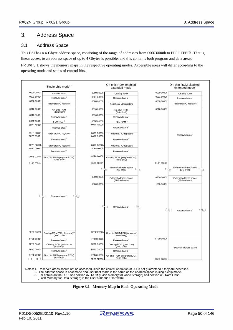
R01DS0052EJ0110 Rev.1.10 Page 50 of 146Feb 10, 2011
RX62N Group, RX621 Group 3. Address Space
3. Address Space
3.1 Address Space
This LSI has a 4-Gbyte address space, consisting of the range of addresses from 0000 0000h to FFFF FFFFh. That is,
linear access to an address space of up to 4 Gbytes is possible, and this contains both program and data areas.
Figure 3.1 shows the memory maps in the respective operating modes. Accessible areas will differ according to the
operating mode and states of control bits.
Figure 3.1 Memory Map in Each Operating Mode
Reserved area*1
Reserved area*1
Notes: 1. Reserved areas should not be accessed, since the correct operation of LSI is not guaranteed if they are accessed. 2. The address space in boot mode and user boot mode is the same as the address space in single-chip mode.3. For details on the FCU, see section 37, ROM (Flash Memory for Code Storage) and section 38, Data Flash
(Flash Memory for Data Storage) in the User’s manual: Hardware.
0000 0000h
0008 0000h
FFFF FFFFh
Single-chip mode*2
On-chip RAM
Reserved area*1
On-chip ROM (program ROM)(read only)
0010 0000h
Peripheral I/O registers
0010 8000h
On-chip ROM (data flash)
0080 0000h
0100 0000h
On-chip ROM (program ROM)(write only)
FFF8 0000h
FCU-RAM*3
Reserved area*1
Peripheral I/O registers
Reserved area*1
Peripheral I/O registers
007F 8000h
007F A000h
007F C000h007F C500h
007F FC00h
0001 8000h
0000 0000h
0008 0000h
FFFF FFFFh
On-chip ROM enabled extended mode
On-chip RAM
Reserved area*1
On-chip ROM (program ROM)(read only)
0010 0000h
Peripheral I/O registers
0010 8000h
On-chip ROM (data flash)
0080 0000h
0100 0000h
On-chip ROM (program ROM)(write only)
0800 0000h
FFF8 0000h
On-chip ROM (FCU firmware)*3
(read only)
FEFF E000h
FF00 0000h
Reserved area*1
FCU-RAM*3
Reserved area*1
Peripheral I/O registers
Reserved area*1
Peripheral I/O registers
007F 8000h
007F A000h
007F C000h007F C500h
007F FC00h
0001 8000h Reserved area*1
External address space(CS area)
0000 0000h
0008 0000h
FFFF FFFFh
On-chip ROM disabled extended mode
On-chip RAM
External address space(CS area)
Reserved area*1
0010 0000h
Peripheral I/O registers
0100 0000h
0800 0000h
FF00 0000h
Reserved area*1
0001 8000hReserved area*1
External address space
Reserved area*1 Reserved area*1
00F8 0000h 00F8 0000h
1000 0000h
On-chip ROM (FCU firmware)*3
(read only)
Reserved area*1
FEFF E000h
FF00 0000h
1000 0000h
External address space(SDRAM area)
External address space(SDRAM area)
FF7F C000h
FF80 C000h
Reserved area*1
On-chip ROM (user boot)(read only)
Reserved area*1
FF7F C000h
FF80 C000h
Reserved area*1
On-chip ROM (user boot)(read only)

R01DS0052EJ0110 Rev.1.10 Page 51 of 146Feb 10, 2011
RX62N Group, RX621 Group 3. Address Space
3.2 External Address Space
The external address space is classified into CS areas (CS0 to CS7) and SDRAM area (SDCS).
The CS area is divided into up to 8 areas (CS0 to CS7), each corresponding to the CSi# signal output from a CSi# (i = 0
to 7) pin.
Figure 3.2 shows the address ranges corresponding to the individual CS areas (CS0 to CS7) and SDRAM area (SDCS)
in on-chip ROM disabled extended mode.
Figure 3.2 Correspondence between External Address Spaces, CS Areas (CS0 to CS7), and SDRAM area (SDCS) (In On-Chip ROM Disabled Extended Mode)
0000 0000h
0008 0000h
On-chip RAM
External address space(CS area)
Reserved area*1
0010 0000h
Peripheral I/O registers
0100 0000h
0800 0000h
FF00 0000h
Reserved area*1
0001 8000hReserved area*1
External address space*2
(CS area)
0100 0000h
0200 0000h
0300 0000h
0400 0000h
0500 0000h
0600 0000h
0700 0000h
CS7 (16 Mbytes)
01FF FFFFh
02FF FFFFh
03FF FFFFh
04FF FFFFh
05FF FFFFh
06FF FFFFh
07FF FFFFh
CS6 (16 Mbytes)
CS5 (16 Mbytes)
CS4 (16 Mbytes)
CS3 (16 Mbytes)
CS2 (16 Mbytes)
CS1 (16 Mbytes)
FFFF FFFFh FFFF FFFFh
FF00 0000h
CS0 (16 Mbytes)
Notes: 1. Reserved areas should not be accessed, since the correct operation of LSI is not guaranteed if they are accessed. 2. The CS0 area is disabled in on-chip ROM enabled extended mode. In this mode, the address space for addresses above 1000 0000h is as shown in figure 4.1.
External address space(SDRAM area)
1000 0000h
0FFF FFFFh
0800 0000h
SDCS (128 Mbytes)

R01DS0052EJ0110 Rev.1.10 Page 52 of 146Feb 10, 2011
RX62N Group, RX621 Group 4. I/O Registers
4. I/O Registers
Table 4.1 List of I/O Registers (Address Order) (1 / 35)
AddressModule Abbreviation Register Name
Register Abbreviation
Number of Bits
AccessSize
Number of Access Cycles
0008 0000h SYSTEM Mode monitor register MDMONR 16 16 3 ICLK
0008 0002h SYSTEM Mode status register MDSR 16 16 3 ICLK
0008 0006h SYSTEM System control register 0 SYSCR0 16 16 3 ICLK
0008 0008h SYSTEM System control register 1 SYSCR1 16 16 3 ICLK
0008 000Ch SYSTEM Standby control register SBYCR 16 16 3 ICLK
0008 0010h SYSTEM Module stop control register A MSTPCRA 32 32 3 ICLK
0008 0014h SYSTEM Module stop control register B MSTPCRB 32 32 3 ICLK
0008 0018h SYSTEM Module stop control register C MSTPCRC 32 32 3 ICLK
0008 0020h SYSTEM System clock control register SCKCR 32 32 3 ICLK
0008 0030h SYSTEM External bus clock control register BCKCR 8 8 3 ICLK
0008 0040h SYSTEM Oscillation stop detection control register OSTDCR 16 16 3 ICLK
0008 1300h BSC Bus error status clear register BERCLR 8 8 2 ICLK
0008 1304h BSC Bus error monitoring enable register BEREN 8 8 2 ICLK
0008 1308h BSC Bus error status register 1 BERSR1 8 8 2 ICLK
0008 130Ah BSC Bus error status register 2 BERSR2 16 16 2 ICLK
0008 2000h DMAC0 DMA source address register DMSAR 32 32 2 ICLK
0008 2004h DMAC0 DMA destination address register DMDAR 32 32 2 ICLK
0008 2008h DMAC0 DMA transfer count register DMCRA 32 32 2 ICLK
0008 200Ch DMAC0 DMA block transfer count register DMCRB 16 16 2 ICLK
0008 2010h DMAC0 DMA transfer mode register DMTMD 16 16 2 ICLK
0008 2013h DMAC0 DMA interrupt setting register DMINT 8 8 2 ICLK
0008 2014h DMAC0 DMA address mode register DMAMD 16 16 2 ICLK
0008 2018h DMAC0 DMA offset register DMOFR 32 32 2 ICLK
0008 201Ch DMAC0 MA transfer enable register DMCNT 8 8 2 ICLK
0008 201Dh DMAC0 DMA software start register DMREQ 8 8 2 ICLK
0008 201Eh DMAC0 DMA status register DMSTS 8 8 2 ICLK
0008 201Fh DMAC0 DMA activation source flag control register
DMCSL 8 8 2 ICLK
0008 2040h DMAC1 DMA source address register DMSAR 32 32 2 ICLK
0008 2044h DMAC1 DMA destination address register DMDAR 32 32 2 ICLK
0008 2048h DMAC1 DMA transfer count register DMCRA 32 32 2 ICLK
0008 204Ch DMAC1 DMA block transfer count register DMCRB 16 16 2 ICLK
0008 2050h DMAC1 DMA transfer mode register DMTMD 16 16 2 ICLK
0008 2053h DMAC1 DMA interrupt setting register DMINT 8 8 2 ICLK
0008 2054h DMAC1 DMA address mode register DMAMD 16 16 2 ICLK
0008 205Ch DMAC1 MA transfer enable register DMCNT 8 8 2 ICLK
0008 205Dh DMAC1 DMA software start register DMREQ 8 8 2 ICLK
0008 205Eh DMAC1 DMA status register DMSTS 8 8 2 ICLK
0008 205Fh DMAC1 DMA activation source flag control register
DMCSL 8 8 2 ICLK
0008 2080h DMAC2 DMA source address register DMSAR 32 32 2 ICLK
0008 2084h DMAC2 DMA destination address register DMDAR 32 32 2 ICLK
0008 2088h DMAC2 DMA transfer count register DMCRA 32 32 2 ICLK
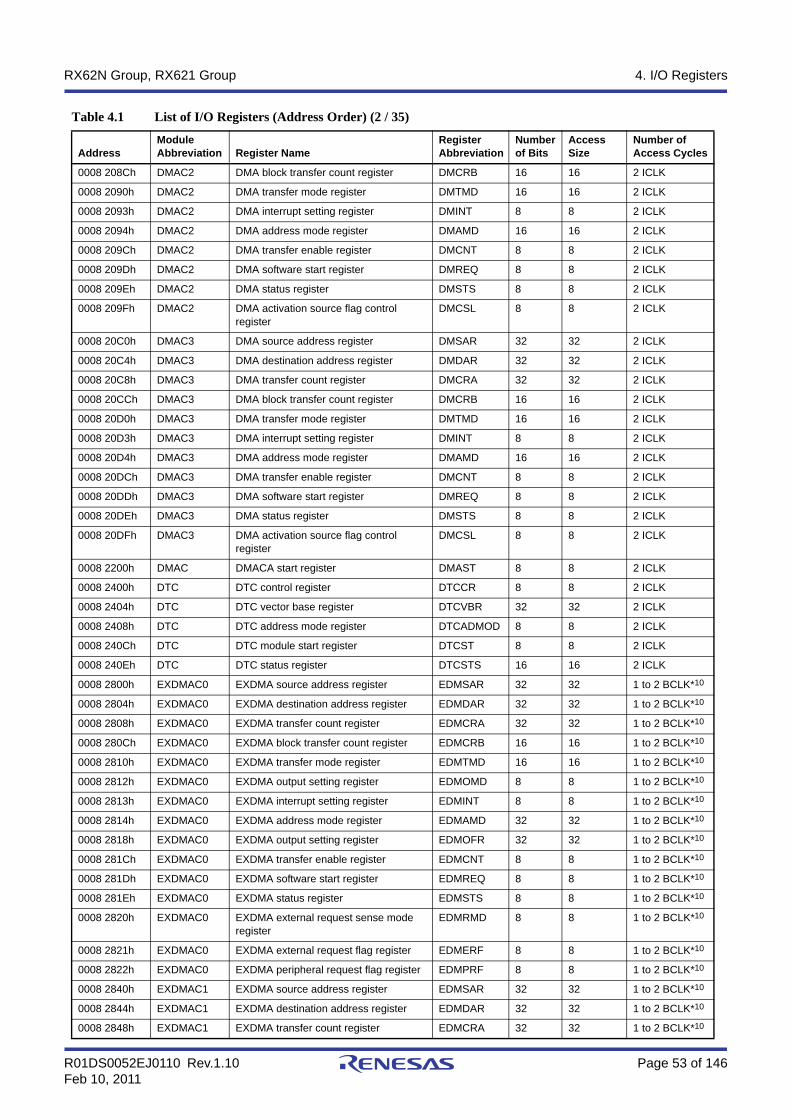
R01DS0052EJ0110 Rev.1.10 Page 53 of 146Feb 10, 2011
RX62N Group, RX621 Group 4. I/O Registers
0008 208Ch DMAC2 DMA block transfer count register DMCRB 16 16 2 ICLK
0008 2090h DMAC2 DMA transfer mode register DMTMD 16 16 2 ICLK
0008 2093h DMAC2 DMA interrupt setting register DMINT 8 8 2 ICLK
0008 2094h DMAC2 DMA address mode register DMAMD 16 16 2 ICLK
0008 209Ch DMAC2 DMA transfer enable register DMCNT 8 8 2 ICLK
0008 209Dh DMAC2 DMA software start register DMREQ 8 8 2 ICLK
0008 209Eh DMAC2 DMA status register DMSTS 8 8 2 ICLK
0008 209Fh DMAC2 DMA activation source flag control register
DMCSL 8 8 2 ICLK
0008 20C0h DMAC3 DMA source address register DMSAR 32 32 2 ICLK
0008 20C4h DMAC3 DMA destination address register DMDAR 32 32 2 ICLK
0008 20C8h DMAC3 DMA transfer count register DMCRA 32 32 2 ICLK
0008 20CCh DMAC3 DMA block transfer count register DMCRB 16 16 2 ICLK
0008 20D0h DMAC3 DMA transfer mode register DMTMD 16 16 2 ICLK
0008 20D3h DMAC3 DMA interrupt setting register DMINT 8 8 2 ICLK
0008 20D4h DMAC3 DMA address mode register DMAMD 16 16 2 ICLK
0008 20DCh DMAC3 DMA transfer enable register DMCNT 8 8 2 ICLK
0008 20DDh DMAC3 DMA software start register DMREQ 8 8 2 ICLK
0008 20DEh DMAC3 DMA status register DMSTS 8 8 2 ICLK
0008 20DFh DMAC3 DMA activation source flag control register
DMCSL 8 8 2 ICLK
0008 2200h DMAC DMACA start register DMAST 8 8 2 ICLK
0008 2400h DTC DTC control register DTCCR 8 8 2 ICLK
0008 2404h DTC DTC vector base register DTCVBR 32 32 2 ICLK
0008 2408h DTC DTC address mode register DTCADMOD 8 8 2 ICLK
0008 240Ch DTC DTC module start register DTCST 8 8 2 ICLK
0008 240Eh DTC DTC status register DTCSTS 16 16 2 ICLK
0008 2800h EXDMAC0 EXDMA source address register EDMSAR 32 32 1 to 2 BCLK*10
0008 2804h EXDMAC0 EXDMA destination address register EDMDAR 32 32 1 to 2 BCLK*10
0008 2808h EXDMAC0 EXDMA transfer count register EDMCRA 32 32 1 to 2 BCLK*10
0008 280Ch EXDMAC0 EXDMA block transfer count register EDMCRB 16 16 1 to 2 BCLK*10
0008 2810h EXDMAC0 EXDMA transfer mode register EDMTMD 16 16 1 to 2 BCLK*10
0008 2812h EXDMAC0 EXDMA output setting register EDMOMD 8 8 1 to 2 BCLK*10
0008 2813h EXDMAC0 EXDMA interrupt setting register EDMINT 8 8 1 to 2 BCLK*10
0008 2814h EXDMAC0 EXDMA address mode register EDMAMD 32 32 1 to 2 BCLK*10
0008 2818h EXDMAC0 EXDMA output setting register EDMOFR 32 32 1 to 2 BCLK*10
0008 281Ch EXDMAC0 EXDMA transfer enable register EDMCNT 8 8 1 to 2 BCLK*10
0008 281Dh EXDMAC0 EXDMA software start register EDMREQ 8 8 1 to 2 BCLK*10
0008 281Eh EXDMAC0 EXDMA status register EDMSTS 8 8 1 to 2 BCLK*10
0008 2820h EXDMAC0 EXDMA external request sense mode register
EDMRMD 8 8 1 to 2 BCLK*10
0008 2821h EXDMAC0 EXDMA external request flag register EDMERF 8 8 1 to 2 BCLK*10
0008 2822h EXDMAC0 EXDMA peripheral request flag register EDMPRF 8 8 1 to 2 BCLK*10
0008 2840h EXDMAC1 EXDMA source address register EDMSAR 32 32 1 to 2 BCLK*10
0008 2844h EXDMAC1 EXDMA destination address register EDMDAR 32 32 1 to 2 BCLK*10
0008 2848h EXDMAC1 EXDMA transfer count register EDMCRA 32 32 1 to 2 BCLK*10
Table 4.1 List of I/O Registers (Address Order) (2 / 35)
AddressModule Abbreviation Register Name
Register Abbreviation
Number of Bits
AccessSize
Number of Access Cycles
R01DS0052EJ0110 Rev.1.10 Page 54 of 146Feb 10, 2011
RX62N Group, RX621 Group 4. I/O Registers
0008 284Ch EXDMAC1 EXDMA block transfer count register EDMCRB 16 16 1 to 2 BCLK*10
0008 2850h EXDMAC1 EXDMA transfer mode register EDMTMD 16 16 1 to 2 BCLK*10
0008 2852h EXDMAC1 EXDMA output setting register EDMOMD 8 8 1 to 2 BCLK*10
0008 2853h EXDMAC1 EXDMA interrupt setting register EDMINT 8 8 1 to 2 BCLK*10
0008 2854h EXDMAC1 EXDMA address mode register EDMAMD 32 32 1 to 2 BCLK*10
0008 285Ch EXDMAC1 EXDMA transfer enable register EDMCNT 8 8 1 to 2 BCLK*10
0008 285Dh EXDMAC1 EXDMA software start register EDMREQ 8 8 1 to 2 BCLK*10
0008 285Eh EXDMAC1 EXDMA status register EDMSTS 8 8 1 to 2 BCLK*10
0008 2860h EXDMAC1 EXDMA external request sense mode register
EDMRMD 8 8 1 to 2 BCLK*10
0008 2861h EXDMAC1 EXDMA external request flag register EDMERF 8 8 1 to 2 BCLK*10
0008 2862h EXDMAC1 EXDMA peripheral request flag register EDMPRF 8 8 1 to 2 BCLK*10
0008 2A00h EXDMAC EXDMA module start register EDMAST 8 8 1 to 2 BCLK*10
0008 2BE0h EXDMAC Cluster buffer register 0 CLSBR0 32 32 1 to 2 BCLK*10
0008 2BE4h EXDMAC Cluster buffer register 1 CLSBR1 32 32 1 to 2 BCLK*10
0008 2BE8h EXDMAC Cluster buffer register 2 CLSBR2 32 32 1 to 2 BCLK*10
0008 2BECh EXDMAC Cluster buffer register 3 CLSBR3 32 32 1 to 2 BCLK*10
0008 2BF0h EXDMAC Cluster buffer register 4 CLSBR4 32 32 1 to 2 BCLK*10
0008 2BF4h EXDMAC Cluster buffer register 5 CLSBR5 32 32 1 to 2 BCLK*10
0008 2BF8h EXDMAC Cluster buffer register 6 CLSBR6 32 32 1 to 2 BCLK*10
0008 3002h BSC CS0 mode register CS0MOD 16 16 1 to 2 BCLK*10
0008 3004h BSC CS0 wait control register 1 CS0WCR1 32 32 1 to 2 BCLK*10
0008 3008h BSC CS0 wait control register 2 CS0WCR2 32 32 1 to 2 BCLK*10
0008 3012h BSC CS1 mode register CS1MOD 16 16 1 to 2 BCLK*10
0008 3014h BSC CS1 wait control register 1 CS1WCR1 32 32 1 to 2 BCLK*10
0008 3018h BSC CS1 wait control register 2 CS1WCR2 32 32 1 to 2 BCLK*10
0008 3022h BSC CS2 mode register CS2MOD 16 16 1 to 2 BCLK*10
0008 3024h BSC CS2 wait control register 1 CS2WCR1 32 32 1 to 2 BCLK*10
0008 3028h BSC CS2 wait control register 2 CS2WCR2 32 32 1 to 2 BCLK*10
0008 3032h BSC CS3 mode register CS3MOD 16 16 1 to 2 BCLK*10
0008 3034h BSC CS3 wait control register 1 CS3WCR1 32 32 1 to 2 BCLK*10
0008 3038h BSC CS3 wait control register 2 CS3WCR2 32 32 1 to 2 BCLK*10
0008 3042h BSC CS4 mode register CS4MOD 16 16 1 to 2 BCLK*10
0008 3044h BSC CS4 wait control register 1 CS4WCR1 32 32 1 to 2 BCLK*10
0008 3048h BSC CS4 wait control register 2 CS4WCR2 32 32 1 to 2 BCLK*10
0008 3052h BSC CS5 mode register CS5MOD 16 16 1 to 2 BCLK*10
0008 3054h BSC CS5 wait control register 1 CS5WCR1 32 32 1 to 2 BCLK*10
0008 3058h BSC CS5 wait control register 2 CS5WCR2 32 32 1 to 2 BCLK*10
0008 3062h BSC CS6 mode register CS6MOD 16 16 1 to 2 BCLK*10
0008 3064h BSC CS6 wait control register 1 CS6WCR1 32 32 1 to 2 BCLK*10
0008 3068h BSC CS6 wait control register 2 CS6WCR2 32 32 1 to 2 BCLK*10
0008 3072h BSC CS7 mode register CS7MOD 16 16 1 to 2 BCLK*10
0008 3074h BSC CS7 wait control register 1 CS7WCR1 32 32 1 to 2 BCLK*10
0008 3078h BSC CS7 wait control register 2 CS7WCR2 32 32 1 to 2 BCLK*10
0008 3802h BSC CS0 control register CS0CR 16 16 1 to 2 BCLK*10
Table 4.1 List of I/O Registers (Address Order) (3 / 35)
AddressModule Abbreviation Register Name
Register Abbreviation
Number of Bits
AccessSize
Number of Access Cycles

R01DS0052EJ0110 Rev.1.10 Page 55 of 146Feb 10, 2011
RX62N Group, RX621 Group 4. I/O Registers
0008 380Ah BSC CS0 recovery cycle register CS0REC 16 16 1 to 2 BCLK*10
0008 3812h BSC CS1 control register CS1CR 16 16 1 to 2 BCLK*10
0008 381Ah BSC CS1 recovery cycle register CS1REC 16 16 1 to 2 BCLK*10
0008 3822h BSC CS2 control register CS2CR 16 16 1 to 2 BCLK*10
0008 382Ah BSC CS2 recovery cycle register CS2REC 16 16 1 to 2 BCLK*10
0008 3832h BSC CS3 control register CS3CR 16 16 1 to 2 BCLK*10
0008 383Ah BSC CS3 recovery cycle register CS3REC 16 16 1 to 2 BCLK*10
0008 3842h BSC CS4 control register CS4CR 16 16 1 to 2 BCLK*10
0008 384Ah BSC CS4 recovery cycle register CS4REC 16 16 1 to 2 BCLK*10
0008 3852h BSC CS5 control register CS5CR 16 16 1 to 2 BCLK*10
0008 385Ah BSC CS5 recovery cycle register CS5REC 16 16 1 to 2 BCLK*10
0008 3862h BSC CS6 control register CS6CR 16 16 1 to 2 BCLK*10
0008 386Ah BSC CS6 recovery cycle register CS6REC 16 16 1 to 2 BCLK*10
0008 3872h BSC CS7 control register CS7CR 16 16 1 to 2 BCLK*10
0008 387Ah BSC CS7 recovery cycle register CS7REC 16 16 1 to 2 BCLK*10
0008 3C00h BSC SDC control register SDCCR 8 8 1 to 2 BCLK*10
0008 3C01h BSC SDC mode register SDCMOD 8 8 1 to 2 BCLK*10
0008 3C02h BSC SDRAM access mode register SDAMOD 8 8 1 to 2 BCLK*10
0008 3C10h BSC SDRAM self-refresh control register SDSELF 8 8 1 to 2 BCLK*10
0008 3C14h BSC SDRAM refresh control register SDRFCR 16 16 1 to 2 BCLK*10
0008 3C16h BSC SDRAM auto-refresh control register SDRFEN 8 8 1 to 2 BCLK*10
0008 3C20h BSC SDRAM initialization sequence control register
SDICR 8 8 1 to 2 BCLK*10
0008 3C24h BSC SDRAM initialization register SDIR 16 16 1 to 2 BCLK*10
0008 3C40h BSC SDRAM address register SDADR 8 8 1 to 2 BCLK*10
0008 3C44h BSC SDRAM timing register SDTR 32 32 1 to 2 BCLK*10
0008 3C48h BSC SDRAM mode register SDMOD 16 16 1 to 2 BCLK*10
0008 3C50h BSC SDRAM status register SDSR 8 8 1 to 2 BCLK*10
0008 7010h ICU Interrupt request register 016 IR016 8 8 2 ICLK
0008 7015h ICU Interrupt request register 021 IR021 8 8 2 ICLK
0008 7017h ICU Interrupt request register 023 IR023 8 8 2 ICLK
0008 701Bh ICU Interrupt request register 027 IR027 8 8 2 ICLK
0008 701Ch ICU Interrupt request register 028 IR028 8 8 2 ICLK
0008 701Dh ICU Interrupt request register 029 IR029 8 8 2 ICLK
0008 701Eh ICU Interrupt request register 030 IR030 8 8 2 ICLK
0008 701Fh ICU Interrupt request register 031 IR031 8 8 2 ICLK
0008 7020h ICU Interrupt request register 032 IR032 8 8 2 ICLK
0008 7024h ICU Interrupt request register 036 IR036 8 8 2 ICLK
0008 7025h ICU Interrupt request register 037 IR037 8 8 2 ICLK
0008 7026h ICU Interrupt request register 038 IR038 8 8 2 ICLK
0008 7028h ICU Interrupt request register 040 IR040 8 8 2 ICLK
0008 7029h ICU Interrupt request register 041 IR041 8 8 2 ICLK
0008 702Ah ICU Interrupt request register 042 IR042 8 8 2 ICLK
0008 702Ch ICU Interrupt request register 044 IR044 8 8 2 ICLK
0008 702Dh ICU Interrupt request register 045 IR045 8 8 2 ICLK
Table 4.1 List of I/O Registers (Address Order) (4 / 35)
AddressModule Abbreviation Register Name
Register Abbreviation
Number of Bits
AccessSize
Number of Access Cycles
R01DS0052EJ0110 Rev.1.10 Page 56 of 146Feb 10, 2011
RX62N Group, RX621 Group 4. I/O Registers
0008 702Eh ICU Interrupt request register 046 IR046 8 8 2 ICLK
0008 702Fh ICU Interrupt request register 047 IR047 8 8 2 ICLK
0008 7030h ICU Interrupt request register 048 IR048 8 8 2 ICLK
0008 7031h ICU Interrupt request register 049 IR049 8 8 2 ICLK
0008 7032h ICU Interrupt request register 050 IR050 8 8 2 ICLK
0008 7033h ICU Interrupt request register 051 IR051 8 8 2 ICLK
0008 7038h ICU Interrupt request register 056 IR056 8 8 2 ICLK
0008 7039h ICU Interrupt request register 057 IR057 8 8 2 ICLK
0008 703Ah ICU Interrupt request register 058 IR058 8 8 2 ICLK
0008 703Bh ICU Interrupt request register 059 IR059 8 8 2 ICLK
0008 703Ch ICU Interrupt request register 060 IR060 8 8 2 ICLK
0008 703Eh ICU Interrupt request register 062 IR062 8 8 2 ICLK
0008 703Fh ICU Interrupt request register 063 IR063 8 8 2 ICLK
0008 7040h ICU Interrupt request register 064 IR064 8 8 2 ICLK
0008 7041h ICU Interrupt request register 065 IR065 8 8 2 ICLK
0008 7042h ICU Interrupt request register 066 IR066 8 8 2 ICLK
0008 7043h ICU Interrupt request register 067 IR067 8 8 2 ICLK
0008 7044h ICU Interrupt request register 068 IR068 8 8 2 ICLK
0008 7045h ICU Interrupt request register 069 IR069 8 8 2 ICLK
0008 7046h ICU Interrupt request register 070 IR070 8 8 2 ICLK
0008 7047h ICU Interrupt request register 071 IR071 8 8 2 ICLK
0008 7048h ICU Interrupt request register 072 IR072 8 8 2 ICLK
0008 7049h ICU Interrupt request register 073 IR073 8 8 2 ICLK
0008 704Ah ICU Interrupt request register 074 IR074 8 8 2 ICLK
0008 704Bh ICU Interrupt request register 075 IR075 8 8 2 ICLK
0008 704Ch ICU Interrupt request register 076 IR076 8 8 2 ICLK
0008 704Dh ICU Interrupt request register 077 IR077 8 8 2 ICLK
0008 704Eh ICU Interrupt request register 078 IR078 8 8 2 ICLK
0008 704Fh ICU Interrupt request register 079 IR079 8 8 2 ICLK
0008 705Ah ICU Interrupt request register 090 IR090 8 8 2 ICLK
0008 705Bh ICU Interrupt request register 091 IR091 8 8 2 ICLK
0008 705Ch ICU Interrupt request register 092 IR092 8 8 2 ICLK
0008 7060h ICU Interrupt request register 096 IR096 8 8 2 ICLK
0008 7062h ICU Interrupt request register 098 IR098 8 8 2 ICLK
0008 7063h ICU Interrupt request register 099 IR099 8 8 2 ICLK
0008 7066h ICU Interrupt request register 102 IR102 8 8 2 ICLK
0008 7072h ICU Interrupt request register 114 IR114 8 8 2 ICLK
0008 7073h ICU Interrupt request register 115 IR115 8 8 2 ICLK
0008 7074h ICU Interrupt request register 116 IR116 8 8 2 ICLK
0008 7075h ICU Interrupt request register 117 IR117 8 8 2 ICLK
0008 7076h ICU Interrupt request register 118 IR118 8 8 2 ICLK
0008 7077h ICU Interrupt request register 119 IR119 8 8 2 ICLK
0008 7078h ICU Interrupt request register 120 IR120 8 8 2 ICLK
0008 7079h ICU Interrupt request register 121 IR121 8 8 2 ICLK
0008 707Ah ICU Interrupt request register 122 IR122 8 8 2 ICLK
Table 4.1 List of I/O Registers (Address Order) (5 / 35)
AddressModule Abbreviation Register Name
Register Abbreviation
Number of Bits
AccessSize
Number of Access Cycles

R01DS0052EJ0110 Rev.1.10 Page 57 of 146Feb 10, 2011
RX62N Group, RX621 Group 4. I/O Registers
0008 707Bh ICU Interrupt request register 123 IR123 8 8 2 ICLK
0008 707Ch ICU Interrupt request register 124 IR124 8 8 2 ICLK
0008 707Dh ICU Interrupt request register 125 IR125 8 8 2 ICLK
0008 707Eh ICU Interrupt request register 126 IR126 8 8 2 ICLK
0008 707Fh ICU Interrupt request register 127 IR127 8 8 2 ICLK
0008 7080h ICU Interrupt request register 128 IR128 8 8 2 ICLK
0008 7081h ICU Interrupt request register 129 IR129 8 8 2 ICLK
0008 7082h ICU Interrupt request register 130 IR130 8 8 2 ICLK
0008 7083h ICU Interrupt request register 131 IR131 8 8 2 ICLK
0008 7084h ICU Interrupt request register 132 IR132 8 8 2 ICLK
0008 7085h ICU Interrupt request register 133 IR133 8 8 2 ICLK
0008 7086h ICU Interrupt request register 134 IR134 8 8 2 ICLK
0008 7087h ICU Interrupt request register 135 IR135 8 8 2 ICLK
0008 7088h ICU Interrupt request register 136 IR136 8 8 2 ICLK
0008 7089h ICU Interrupt request register 137 IR137 8 8 2 ICLK
0008 708Ah ICU Interrupt request register 138 IR138 8 8 2 ICLK
0008 708Bh ICU Interrupt request register 139 IR139 8 8 2 ICLK
0008 708Ch ICU Interrupt request register 140 IR140 8 8 2 ICLK
0008 708Dh ICU Interrupt request register 141 IR141 8 8 2 ICLK
0008 708Eh ICU Interrupt request register 142 IR142 8 8 2 ICLK
0008 708Fh ICU Interrupt request register 143 IR143 8 8 2 ICLK
0008 7090h ICU Interrupt request register 144 IR144 8 8 2 ICLK
0008 7091h ICU Interrupt request register 145 IR145 8 8 2 ICLK
0008 7092h ICU Interrupt request register 146 IR146 8 8 2 ICLK
0008 7093h ICU Interrupt request register 147 IR147 8 8 2 ICLK
0008 7094h ICU Interrupt request register 148 IR148 8 8 2 ICLK
0008 7095h ICU Interrupt request register 149 IR149 8 8 2 ICLK
0008 7096h ICU Interrupt request register 150 IR150 8 8 2 ICLK
0008 7097h ICU Interrupt request register 151 IR151 8 8 2 ICLK
0008 7098h ICU Interrupt request register 152 IR152 8 8 2 ICLK
0008 7099h ICU Interrupt request register 153 IR153 8 8 2 ICLK
0008 709Ah ICU Interrupt request register 154 IR154 8 8 2 ICLK
0008 709Bh ICU Interrupt request register 155 IR155 8 8 2 ICLK
0008 709Ch ICU Interrupt request register 156 IR156 8 8 2 ICLK
0008 709Dh ICU Interrupt request register 157 IR157 8 8 2 ICLK
0008 709Eh ICU Interrupt request register 158 IR158 8 8 2 ICLK
0008 709Fh ICU Interrupt request register 159 IR159 8 8 2 ICLK
0008 70A0h ICU Interrupt request register 160 IR160 8 8 2 ICLK
0008 70A1h ICU Interrupt request register 161 IR161 8 8 2 ICLK
0008 70A2h ICU Interrupt request register 162 IR162 8 8 2 ICLK
0008 70A3h ICU Interrupt request register 163 IR163 8 8 2 ICLK
0008 70A4h ICU Interrupt request register 164 IR164 8 8 2 ICLK
0008 70A5h ICU Interrupt request register 165 IR165 8 8 2 ICLK
0008 70A6h ICU Interrupt request register 166 IR166 8 8 2 ICLK
0008 70A7h ICU Interrupt request register 167 IR167 8 8 2 ICLK
Table 4.1 List of I/O Registers (Address Order) (6 / 35)
AddressModule Abbreviation Register Name
Register Abbreviation
Number of Bits
AccessSize
Number of Access Cycles
R01DS0052EJ0110 Rev.1.10 Page 58 of 146Feb 10, 2011
RX62N Group, RX621 Group 4. I/O Registers
0008 70A8h ICU Interrupt request register 168 IR168 8 8 2 ICLK
0008 70A9h ICU Interrupt request register 169 IR169 8 8 2 ICLK
0008 70AAh ICU Interrupt request register 170 IR170 8 8 2 ICLK
0008 70ABh ICU Interrupt request register 171 IR171 8 8 2 ICLK
0008 70ACh ICU Interrupt request register 172 IR172 8 8 2 ICLK
0008 70ADh ICU Interrupt request register 173 IR173 8 8 2 ICLK
0008 70AEh ICU Interrupt request register 174 IR174 8 8 2 ICLK
0008 70AFh ICU Interrupt request register 175 IR175 8 8 2 ICLK
0008 70B0h ICU Interrupt request register 176 IR176 8 8 2 ICLK
0008 70B1h ICU Interrupt request register 177 IR177 8 8 2 ICLK
0008 70B2h ICU Interrupt request register 178 IR178 8 8 2 ICLK
0008 70B3h ICU Interrupt request register 179 IR179 8 8 2 ICLK
0008 70B4h ICU Interrupt request register 180 IR180 8 8 2 ICLK
0008 70B5h ICU Interrupt request register 181 IR181 8 8 2 ICLK
0008 70B6h ICU Interrupt request register 182 IR182 8 8 2 ICLK
0008 70B7h ICU Interrupt request register 183 IR183 8 8 2 ICLK
0008 70B8h ICU Interrupt request register 184 IR184 8 8 2 ICLK
0008 70B9h ICU Interrupt request register 185 IR185 8 8 2 ICLK
0008 70C6h ICU Interrupt request register 198 IR198 8 8 2 ICLK
0008 70C7h ICU Interrupt request register 199 IR199 8 8 2 ICLK
0008 70C8h ICU Interrupt request register 200 IR200 8 8 2 ICLK
0008 70C9h ICU Interrupt request register 201 IR201 8 8 2 ICLK
0008 70CAh ICU Interrupt request register 202 IR202 8 8 2 ICLK
0008 70CBh ICU Interrupt request register 203 IR203 8 8 2 ICLK
0008 70D6h ICU Interrupt request register 214 IR214 8 8 2 ICLK
0008 70D7h ICU Interrupt request register 215 IR215 8 8 2 ICLK
0008 70D8h ICU Interrupt request register 216 IR216 8 8 2 ICLK
0008 70D9h ICU Interrupt request register 217 IR217 8 8 2 ICLK
0008 70DAh ICU Interrupt request register 218 IR218 8 8 2 ICLK
0008 70DBh ICU Interrupt request register 219 IR219 8 8 2 ICLK
0008 70DCh ICU Interrupt request register 220 IR220 8 8 2 ICLK
0008 70DDh ICU Interrupt request register 221 IR221 8 8 2 ICLK
0008 70DEh ICU Interrupt request register 222 IR222 8 8 2 ICLK
0008 70DFh ICU Interrupt request register 223 IR223 8 8 2 ICLK
0008 70E0h ICU Interrupt request register 224 IR224 8 8 2 ICLK
0008 70E1h ICU Interrupt request register 225 IR225 8 8 2 ICLK
0008 70E2h ICU Interrupt request register 226 IR226 8 8 2 ICLK
0008 70E3h ICU Interrupt request register 227 IR227 8 8 2 ICLK
0008 70E4h ICU Interrupt request register 228 IR228 8 8 2 ICLK
0008 70E5h ICU Interrupt request register 229 IR229 8 8 2 ICLK
0008 70EAh ICU Interrupt request register 234 IR234 8 8 2 ICLK
0008 70EBh ICU Interrupt request register 235 IR235 8 8 2 ICLK
0008 70ECh ICU Interrupt request register 236 IR236 8 8 2 ICLK
0008 70EDh ICU Interrupt request register 237 IR237 8 8 2 ICLK
0008 70EEh ICU Interrupt request register 238 IR238 8 8 2 ICLK
Table 4.1 List of I/O Registers (Address Order) (7 / 35)
AddressModule Abbreviation Register Name
Register Abbreviation
Number of Bits
AccessSize
Number of Access Cycles
R01DS0052EJ0110 Rev.1.10 Page 59 of 146Feb 10, 2011
RX62N Group, RX621 Group 4. I/O Registers
0008 70EFh ICU Interrupt request register 239 IR239 8 8 2 ICLK
0008 70F0h ICU Interrupt request register 240 IR240 8 8 2 ICLK
0008 70F1h ICU Interrupt request register 241 IR241 8 8 2 ICLK
0008 70F6h ICU Interrupt request register 246 IR246 8 8 2 ICLK
0008 70F7h ICU Interrupt request register 247 IR247 8 8 2 ICLK
0008 70F8h ICU Interrupt request register 248 IR248 8 8 2 ICLK
0008 70F9h ICU Interrupt request register 249 IR249 8 8 2 ICLK
0008 70FAh ICU Interrupt request register 250 IR250 8 8 2 ICLK
0008 70FBh ICU Interrupt request register 251 IR251 8 8 2 ICLK
0008 70FCh ICU Interrupt request register 252 IR252 8 8 2 ICLK
0008 70FDh ICU Interrupt request register 253 IR253 8 8 2 ICLK
0008 711Bh ICU DTC activation enable register 027 DTCER027 8 8 2 ICLK
0008 711Ch ICU DTC activation enable register 028 DTCER028 8 8 2 ICLK
0008 711Dh ICU DTC activation enable register 029 DTCER029 8 8 2 ICLK
0008 711Eh ICU DTC activation enable register 030 DTCER030 8 8 2 ICLK
0008 711Fh ICU DTC activation enable register 031 DTCER031 8 8 2 ICLK
0008 7124h ICU DTC activation enable register 036 DTCER036 8 8 2 ICLK
0008 7125h ICU DTC activation enable register 037 DTCER037 8 8 2 ICLK
0008 7128h ICU DTC activation enable register 040 DTCER040 8 8 2 ICLK
0008 7129h ICU DTC activation enable register 041 DTCER041 8 8 2 ICLK
0008 712Dh ICU DTC activation enable register 045 DTCER045 8 8 2 ICLK
0008 712Eh ICU DTC activation enable register 046 DTCER046 8 8 2 ICLK
0008 7131h ICU DTC activation enable register 049 DTCER049 8 8 2 ICLK
0008 7132h ICU DTC activation enable register 050 DTCER050 8 8 2 ICLK
0008 7140h ICU DTC activation enable register 064 DTCER064 8 8 2 ICLK
0008 7141h ICU DTC activation enable register 065 DTCER065 8 8 2 ICLK
0008 7142h ICU DTC activation enable register 066 DTCER066 8 8 2 ICLK
0008 7143h ICU DTC activation enable register 067 DTCER067 8 8 2 ICLK
0008 7144h ICU DTC activation enable register 068 DTCER068 8 8 2 ICLK
0008 7145h ICU DTC activation enable register 069 DTCER069 8 8 2 ICLK
0008 7146h ICU DTC activation enable register 070 DTCER070 8 8 2 ICLK
0008 7147h ICU DTC activation enable register 071 DTCER071 8 8 2 ICLK
0008 7148h ICU DTC activation enable register 072 DTCER072 8 8 2 ICLK
0008 7149h ICU DTC activation enable register 073 DTCER073 8 8 2 ICLK
0008 714Ah ICU DTC activation enable register 074 DTCER074 8 8 2 ICLK
0008 714Bh ICU DTC activation enable register 075 DTCER075 8 8 2 ICLK
0008 714Ch ICU DTC activation enable register 076 DTCER076 8 8 2 ICLK
0008 714Dh ICU DTC activation enable register 077 DTCER077 8 8 2 ICLK
0008 714Eh ICU DTC activation enable register 078 DTCER078 8 8 2 ICLK
0008 714Fh ICU DTC activation enable register 079 DTCER079 8 8 2 ICLK
0008 7162h ICU DTC activation enable register 098 DTCER098 8 8 2 ICLK
0008 7163h ICU DTC activation enable register 099 DTCER099 8 8 2 ICLK
0008 7166h ICU DTC activation enable register 102 DTCER102 8 8 2 ICLK
0008 7172h ICU DTC activation enable register 114 DTCER114 8 8 2 ICLK
0008 7173h ICU DTC activation enable register 115 DTCER115 8 8 2 ICLK
Table 4.1 List of I/O Registers (Address Order) (8 / 35)
AddressModule Abbreviation Register Name
Register Abbreviation
Number of Bits
AccessSize
Number of Access Cycles
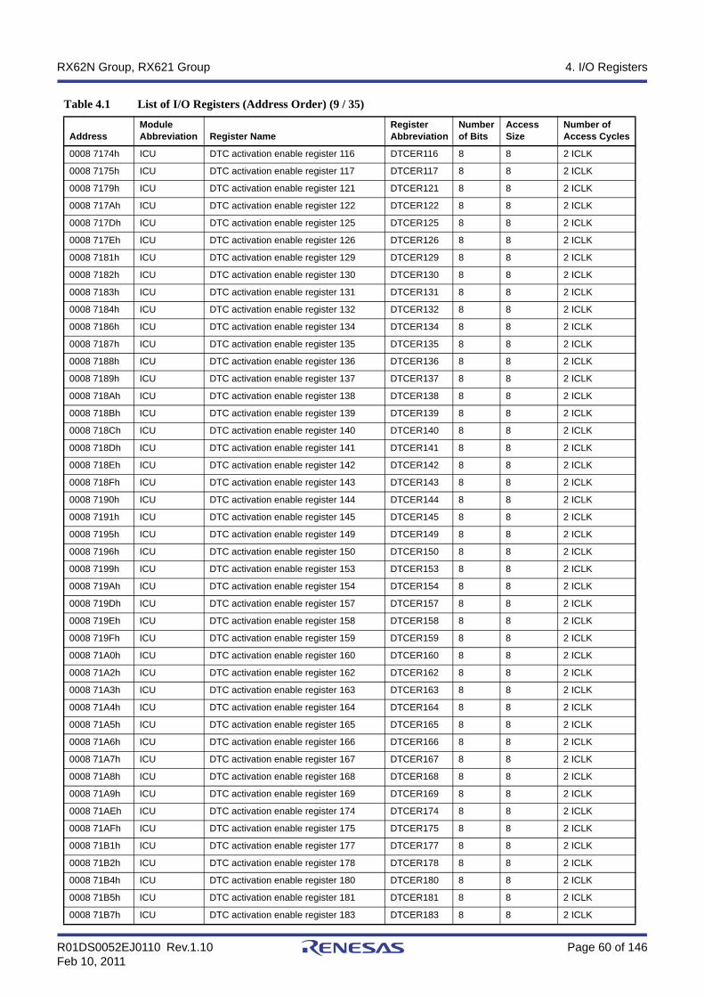
R01DS0052EJ0110 Rev.1.10 Page 60 of 146Feb 10, 2011
RX62N Group, RX621 Group 4. I/O Registers
0008 7174h ICU DTC activation enable register 116 DTCER116 8 8 2 ICLK
0008 7175h ICU DTC activation enable register 117 DTCER117 8 8 2 ICLK
0008 7179h ICU DTC activation enable register 121 DTCER121 8 8 2 ICLK
0008 717Ah ICU DTC activation enable register 122 DTCER122 8 8 2 ICLK
0008 717Dh ICU DTC activation enable register 125 DTCER125 8 8 2 ICLK
0008 717Eh ICU DTC activation enable register 126 DTCER126 8 8 2 ICLK
0008 7181h ICU DTC activation enable register 129 DTCER129 8 8 2 ICLK
0008 7182h ICU DTC activation enable register 130 DTCER130 8 8 2 ICLK
0008 7183h ICU DTC activation enable register 131 DTCER131 8 8 2 ICLK
0008 7184h ICU DTC activation enable register 132 DTCER132 8 8 2 ICLK
0008 7186h ICU DTC activation enable register 134 DTCER134 8 8 2 ICLK
0008 7187h ICU DTC activation enable register 135 DTCER135 8 8 2 ICLK
0008 7188h ICU DTC activation enable register 136 DTCER136 8 8 2 ICLK
0008 7189h ICU DTC activation enable register 137 DTCER137 8 8 2 ICLK
0008 718Ah ICU DTC activation enable register 138 DTCER138 8 8 2 ICLK
0008 718Bh ICU DTC activation enable register 139 DTCER139 8 8 2 ICLK
0008 718Ch ICU DTC activation enable register 140 DTCER140 8 8 2 ICLK
0008 718Dh ICU DTC activation enable register 141 DTCER141 8 8 2 ICLK
0008 718Eh ICU DTC activation enable register 142 DTCER142 8 8 2 ICLK
0008 718Fh ICU DTC activation enable register 143 DTCER143 8 8 2 ICLK
0008 7190h ICU DTC activation enable register 144 DTCER144 8 8 2 ICLK
0008 7191h ICU DTC activation enable register 145 DTCER145 8 8 2 ICLK
0008 7195h ICU DTC activation enable register 149 DTCER149 8 8 2 ICLK
0008 7196h ICU DTC activation enable register 150 DTCER150 8 8 2 ICLK
0008 7199h ICU DTC activation enable register 153 DTCER153 8 8 2 ICLK
0008 719Ah ICU DTC activation enable register 154 DTCER154 8 8 2 ICLK
0008 719Dh ICU DTC activation enable register 157 DTCER157 8 8 2 ICLK
0008 719Eh ICU DTC activation enable register 158 DTCER158 8 8 2 ICLK
0008 719Fh ICU DTC activation enable register 159 DTCER159 8 8 2 ICLK
0008 71A0h ICU DTC activation enable register 160 DTCER160 8 8 2 ICLK
0008 71A2h ICU DTC activation enable register 162 DTCER162 8 8 2 ICLK
0008 71A3h ICU DTC activation enable register 163 DTCER163 8 8 2 ICLK
0008 71A4h ICU DTC activation enable register 164 DTCER164 8 8 2 ICLK
0008 71A5h ICU DTC activation enable register 165 DTCER165 8 8 2 ICLK
0008 71A6h ICU DTC activation enable register 166 DTCER166 8 8 2 ICLK
0008 71A7h ICU DTC activation enable register 167 DTCER167 8 8 2 ICLK
0008 71A8h ICU DTC activation enable register 168 DTCER168 8 8 2 ICLK
0008 71A9h ICU DTC activation enable register 169 DTCER169 8 8 2 ICLK
0008 71AEh ICU DTC activation enable register 174 DTCER174 8 8 2 ICLK
0008 71AFh ICU DTC activation enable register 175 DTCER175 8 8 2 ICLK
0008 71B1h ICU DTC activation enable register 177 DTCER177 8 8 2 ICLK
0008 71B2h ICU DTC activation enable register 178 DTCER178 8 8 2 ICLK
0008 71B4h ICU DTC activation enable register 180 DTCER180 8 8 2 ICLK
0008 71B5h ICU DTC activation enable register 181 DTCER181 8 8 2 ICLK
0008 71B7h ICU DTC activation enable register 183 DTCER183 8 8 2 ICLK
Table 4.1 List of I/O Registers (Address Order) (9 / 35)
AddressModule Abbreviation Register Name
Register Abbreviation
Number of Bits
AccessSize
Number of Access Cycles

R01DS0052EJ0110 Rev.1.10 Page 61 of 146Feb 10, 2011
RX62N Group, RX621 Group 4. I/O Registers
0008 71B8h ICU DTC activation enable register 184 DTCER184 8 8 2 ICLK
0008 71C6h ICU DTC activation enable register 198 DTCER198 8 8 2 ICLK
0008 71C7h ICU DTC activation enable register 199 DTCER199 8 8 2 ICLK
0008 71C8h ICU DTC activation enable register 200 DTCER200 8 8 2 ICLK
0008 71C9h ICU DTC activation enable register 201 DTCER201 8 8 2 ICLK
0008 71CAh ICU DTC activation enable register 202 DTCER202 8 8 2 ICLK
0008 71CBh ICU DTC activation enable register 203 DTCER203 8 8 2 ICLK
0008 71D7h ICU DTC activation enable register 215 DTCER215 8 8 2 ICLK
0008 71D8h ICU DTC activation enable register 216 DTCER216 8 8 2 ICLK
0008 71DBh ICU DTC activation enable register 219 DTCER219 8 8 2 ICLK
0008 71DCh ICU DTC activation enable register 220 DTCER220 8 8 2 ICLK
0008 71DFh ICU DTC activation enable register 223 DTCER223 8 8 2 ICLK
0008 71E0h ICU DTC activation enable register 224 DTCER224 8 8 2 ICLK
0008 71E3h ICU DTC activation enable register 227 DTCER227 8 8 2 ICLK
0008 71E4h ICU DTC activation enable register 228 DTCER228 8 8 2 ICLK
0008 71EBh ICU DTC activation enable register 235 DTCER235 8 8 2 ICLK
0008 71ECh ICU DTC activation enable register 236 DTCER236 8 8 2 ICLK
0008 71EFh ICU DTC activation enable register 239 DTCER239 8 8 2 ICLK
0008 71F0h ICU DTC activation enable register 240 DTCER240 8 8 2 ICLK
0008 71F7h ICU DTC activation enable register 247 DTCER247 8 8 2 ICLK
0008 71F8h ICU DTC activation enable register 248 DTCER248 8 8 2 ICLK
0008 71FBh ICU DTC activation enable register 251 DTCER251 8 8 2 ICLK
0008 71FCh ICU DTC activation enable register 252 DTCER252 8 8 2 ICLK
0008 7202h ICU Interrupt request enable register 02 IER02 8 8 2 ICLK
0008 7203h ICU Interrupt request enable register 03 IER03 8 8 2 ICLK
0008 7204h ICU Interrupt request enable register 04 IER04 8 8 2 ICLK
0008 7205h ICU Interrupt request enable register 05 IER05 8 8 2 ICLK
0008 7206h ICU Interrupt request enable register 06 IER06 8 8 2 ICLK
0008 7207h ICU Interrupt request enable register 07 IER07 8 8 2 ICLK
0008 7208h ICU Interrupt request enable register 08 IER08 8 8 2 ICLK
0008 7209h ICU Interrupt request enable register 09 IER09 8 8 2 ICLK
0008 720Bh ICU Interrupt request enable register 0B IER0B 8 8 2 ICLK
0008 720Ch ICU Interrupt request enable register 0C IER0C 8 8 2 ICLK
0008 720Eh ICU Interrupt request enable register 0E IER0E 8 8 2 ICLK
0008 720Fh ICU Interrupt request enable register 0F IER0F 8 8 2 ICLK
0008 7210h ICU Interrupt request enable register 10 IER10 8 8 2 ICLK
0008 7211h ICU Interrupt request enable register 11 IER11 8 8 2 ICLK
0008 7212h ICU Interrupt request enable register 12 IER12 8 8 2 ICLK
0008 7213h ICU Interrupt request enable register 13 IER13 8 8 2 ICLK
0008 7214h ICU Interrupt request enable register 14 IER14 8 8 2 ICLK
0008 7215h ICU Interrupt request enable register 15 IER15 8 8 2 ICLK
0008 7216h ICU Interrupt request enable register 16 IER16 8 8 2 ICLK
0008 7217h ICU Interrupt request enable register 17 IER17 8 8 2 ICLK
0008 7218h ICU Interrupt request enable register 18 IER18 8 8 2 ICLK
0008 7219h ICU Interrupt request enable register 19 IER19 8 8 2 ICLK
Table 4.1 List of I/O Registers (Address Order) (10 / 35)
AddressModule Abbreviation Register Name
Register Abbreviation
Number of Bits
AccessSize
Number of Access Cycles
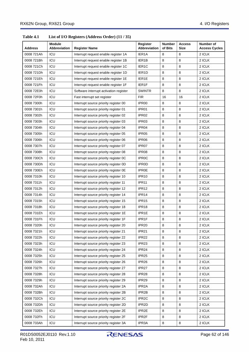
R01DS0052EJ0110 Rev.1.10 Page 62 of 146Feb 10, 2011
RX62N Group, RX621 Group 4. I/O Registers
0008 721Ah ICU Interrupt request enable register 1A IER1A 8 8 2 ICLK
0008 721Bh ICU Interrupt request enable register 1B IER1B 8 8 2 ICLK
0008 721Ch ICU Interrupt request enable register 1C IER1C 8 8 2 ICLK
0008 721Dh ICU Interrupt request enable register 1D IER1D 8 8 2 ICLK
0008 721Eh ICU Interrupt request enable register 1E IER1E 8 8 2 ICLK
0008 721Fh ICU Interrupt request enable register 1F IER1F 8 8 2 ICLK
0008 72E0h ICU Software interrupt activation register SWINTR 8 8 2 ICLK
0008 72F0h ICU Fast interrupt set register FIR 16 16 2 ICLK
0008 7300h ICU Interrupt source priority register 00 IPR00 8 8 2 ICLK
0008 7301h ICU Interrupt source priority register 01 IPR01 8 8 2 ICLK
0008 7302h ICU Interrupt source priority register 02 IPR02 8 8 2 ICLK
0008 7303h ICU Interrupt source priority register 03 IPR03 8 8 2 ICLK
0008 7304h ICU Interrupt source priority register 04 IPR04 8 8 2 ICLK
0008 7305h ICU Interrupt source priority register 05 IPR05 8 8 2 ICLK
0008 7306h ICU Interrupt source priority register 06 IPR06 8 8 2 ICLK
0008 7307h ICU Interrupt source priority register 07 IPR07 8 8 2 ICLK
0008 7308h ICU Interrupt source priority register 08 IPR08 8 8 2 ICLK
0008 730Ch ICU Interrupt source priority register 0C IPR0C 8 8 2 ICLK
0008 730Dh ICU Interrupt source priority register 0D IPR0D 8 8 2 ICLK
0008 730Eh ICU Interrupt source priority register 0E IPR0E 8 8 2 ICLK
0008 7310h ICU Interrupt source priority register 10 IPR10 8 8 2 ICLK
0008 7311h ICU Interrupt source priority register 11 IPR11 8 8 2 ICLK
0008 7312h ICU Interrupt source priority register 12 IPR12 8 8 2 ICLK
0008 7314h ICU Interrupt source priority register 14 IPR14 8 8 2 ICLK
0008 7315h ICU Interrupt source priority register 15 IPR15 8 8 2 ICLK
0008 7318h ICU Interrupt source priority register 18 IPR18 8 8 2 ICLK
0008 731Eh ICU Interrupt source priority register 1E IPR1E 8 8 2 ICLK
0008 731Fh ICU Interrupt source priority register 1F IPR1F 8 8 2 ICLK
0008 7320h ICU Interrupt source priority register 20 IPR20 8 8 2 ICLK
0008 7321h ICU Interrupt source priority register 21 IPR21 8 8 2 ICLK
0008 7322h ICU Interrupt source priority register 22 IPR22 8 8 2 ICLK
0008 7323h ICU Interrupt source priority register 23 IPR23 8 8 2 ICLK
0008 7324h ICU Interrupt source priority register 24 IPR24 8 8 2 ICLK
0008 7325h ICU Interrupt source priority register 25 IPR25 8 8 2 ICLK
0008 7326h ICU Interrupt source priority register 26 IPR26 8 8 2 ICLK
0008 7327h ICU Interrupt source priority register 27 IPR27 8 8 2 ICLK
0008 7328h ICU Interrupt source priority register 28 IPR28 8 8 2 ICLK
0008 7329h ICU Interrupt source priority register 29 IPR29 8 8 2 ICLK
0008 732Ah ICU Interrupt source priority register 2A IPR2A 8 8 2 ICLK
0008 732Bh ICU Interrupt source priority register 2B IPR2B 8 8 2 ICLK
0008 732Ch ICU Interrupt source priority register 2C IPR2C 8 8 2 ICLK
0008 732Dh ICU Interrupt source priority register 2D IPR2D 8 8 2 ICLK
0008 732Eh ICU Interrupt source priority register 2E IPR2E 8 8 2 ICLK
0008 732Fh ICU Interrupt source priority register 2F IPR2F 8 8 2 ICLK
0008 733Ah ICU Interrupt source priority register 3A IPR3A 8 8 2 ICLK
Table 4.1 List of I/O Registers (Address Order) (11 / 35)
AddressModule Abbreviation Register Name
Register Abbreviation
Number of Bits
AccessSize
Number of Access Cycles

R01DS0052EJ0110 Rev.1.10 Page 63 of 146Feb 10, 2011
RX62N Group, RX621 Group 4. I/O Registers
0008 733Bh ICU Interrupt source priority register 3B IPR3B 8 8 2 ICLK
0008 733Ch ICU Interrupt source priority register 3C IPR3C 8 8 2 ICLK
0008 7340h ICU Interrupt source priority register 40 IPR40 8 8 2 ICLK
0008 7344h ICU Interrupt source priority register 44 IPR44 8 8 2 ICLK
0008 7345h ICU Interrupt source priority register 45 IPR45 8 8 2 ICLK
0008 7348h ICU Interrupt source priority register 48 IPR48 8 8 2 ICLK
0008 7351h ICU Interrupt source priority register 51 IPR51 8 8 2 ICLK
0008 7352h ICU Interrupt source priority register 52 IPR52 8 8 2 ICLK
0008 7353h ICU Interrupt source priority register 53 IPR53 8 8 2 ICLK
0008 7354h ICU Interrupt source priority register 54 IPR54 8 8 2 ICLK
0008 7355h ICU Interrupt source priority register 55 IPR55 8 8 2 ICLK
0008 7356h ICU Interrupt source priority register 56 IPR56 8 8 2 ICLK
0008 7357h ICU Interrupt source priority register 57 IPR57 8 8 2 ICLK
0008 7358h ICU Interrupt source priority register 58 IPR58 8 8 2 ICLK
0008 7359h ICU Interrupt source priority register 59 IPR59 8 8 2 ICLK
0008 735Ah ICU Interrupt source priority register 5A IPR5A 8 8 2 ICLK
0008 735Bh ICU Interrupt source priority register 5B IPR5B 8 8 2 ICLK
0008 735Ch ICU Interrupt source priority register 5C IPR5C 8 8 2 ICLK
0008 735Dh ICU Interrupt source priority register 5D IPR5D 8 8 2 ICLK
0008 735Eh ICU Interrupt source priority register 5E IPR5E 8 8 2 ICLK
0008 735Fh ICU Interrupt source priority register 5F IPR5F 8 8 2 ICLK
0008 7360h ICU Interrupt source priority register 60 IPR60 8 8 2 ICLK
0008 7361h ICU Interrupt source priority register 61 IPR61 8 8 2 ICLK
0008 7362h ICU Interrupt source priority register 62 IPR62 8 8 2 ICLK
0008 7363h ICU Interrupt source priority register 63 IPR63 8 8 2 ICLK
0008 7364h ICU Interrupt source priority register 64 IPR64 8 8 2 ICLK
0008 7365h ICU Interrupt source priority register 65 IPR65 8 8 2 ICLK
0008 7366h ICU Interrupt source priority register 66 IPR66 8 8 2 ICLK
0008 7367h ICU Interrupt source priority register 67 IPR67 8 8 2 ICLK
0008 7368h ICU Interrupt source priority register 68 IPR68 8 8 2 ICLK
0008 7369h ICU Interrupt source priority register 69 IPR69 8 8 2 ICLK
0008 736Ah ICU Interrupt source priority register 6A IPR6A 8 8 2 ICLK
0008 736Bh ICU Interrupt source priority register 6B IPR6B 8 8 2 ICLK
0008 7370h ICU Interrupt source priority register 70 IPR70 8 8 2 ICLK
0008 7371h ICU Interrupt source priority register 71 IPR71 8 8 2 ICLK
0008 7372h ICU Interrupt source priority register 72 IPR72 8 8 2 ICLK
0008 7373h ICU Interrupt source priority register 73 IPR73 8 8 2 ICLK
0008 7374h ICU Interrupt source priority register 74 IPR74 8 8 2 ICLK
0008 7375h ICU Interrupt source priority register 75 IPR75 8 8 2 ICLK
0008 7380h ICU Interrupt source priority register 80 IPR80 8 8 2 ICLK
0008 7381h ICU Interrupt source priority register 81 IPR81 8 8 2 ICLK
0008 7382h ICU Interrupt source priority register 82 IPR82 8 8 2 ICLK
0008 7383h ICU Interrupt source priority register 83 IPR83 8 8 2 ICLK
0008 7385h ICU Interrupt source priority register 85 IPR85 8 8 2 ICLK
0008 7386h ICU Interrupt source priority register 86 IPR86 8 8 2 ICLK
Table 4.1 List of I/O Registers (Address Order) (12 / 35)
AddressModule Abbreviation Register Name
Register Abbreviation
Number of Bits
AccessSize
Number of Access Cycles

R01DS0052EJ0110 Rev.1.10 Page 64 of 146Feb 10, 2011
RX62N Group, RX621 Group 4. I/O Registers
0008 7388h ICU Interrupt source priority register 88 IPR88 8 8 2 ICLK
0008 7389h ICU Interrupt source priority register 89 IPR89 8 8 2 ICLK
0008 738Ah ICU Interrupt source priority register 8A IPR8A 8 8 2 ICLK
0008 738Bh ICU Interrupt source priority register 8B IPR8B 8 8 2 ICLK
0008 738Ch ICU Interrupt source priority register 8C IPR8C 8 8 2 ICLK
0008 738Dh ICU Interrupt source priority register 8D IPR8D 8 8 2 ICLK
0008 738Eh ICU Interrupt source priority register 8E IPR8E 8 8 2 ICLK
0008 738Fh ICU Interrupt source priority register 8F IPR8F 8 8 2 ICLK
0008 7400h ICU DMACA activation source select register 0 DMRSR0 8 8 2 ICLK
0008 7404h ICU DMACA activation source select register 1 DMRSR1 8 8 2 ICLK
0008 7408h ICU DMACA activation source select register 2 DMRSR2 8 8 2 ICLK
0008 740Ch ICU DMACA activation source select register 3 DMRSR3 8 8 2 ICLK
0008 7500h ICU IRQ control register 0 IRQCR0 8 8 2 ICLK
0008 7501h ICU IRQ control register 1 IRQCR1 8 8 2 ICLK
0008 7502h ICU IRQ control register 2 IRQCR2 8 8 2 ICLK
0008 7503h ICU IRQ control register 3 IRQCR3 8 8 2 ICLK
0008 7504h ICU IRQ control register 4 IRQCR4 8 8 2 ICLK
0008 7505h ICU IRQ control register 5 IRQCR5 8 8 2 ICLK
0008 7506h ICU IRQ control register 6 IRQCR6 8 8 2 ICLK
0008 7507h ICU IRQ control register 7 IRQCR7 8 8 2 ICLK
0008 7508h ICU IRQ control register 8 IRQCR8 8 8 2 ICLK
0008 7509h ICU IRQ control register 9 IRQCR9 8 8 2 ICLK
0008 750Ah ICU IRQ control register 10 IRQCR10 8 8 2 ICLK
0008 750Bh ICU IRQ control register 11 IRQCR11 8 8 2 ICLK
0008 750Ch ICU IRQ control register 12 IRQCR12 8 8 2 ICLK
0008 750Dh ICU IRQ control register 13 IRQCR13 8 8 2 ICLK
0008 750Eh ICU IRQ control register 14 IRQCR14 8 8 2 ICLK
0008 750Fh ICU IRQ control register 15 IRQCR15 8 8 2 ICLK
0008 7580h ICU Non-maskable interrupt status register NMISR 8 8 2 ICLK
0008 7581h ICU Non-maskable interrupt enable register NMIER 8 8 2 ICLK
0008 7582h ICU Non-maskable interrupt clear register NMICLR 8 8 2 ICLK
0008 7583h ICU NMI pin interrupt control register NMICR 8 8 2 ICLK
0008 8000h CMT Compare match timer start register 0 CMSTR0 16 16 2 to 3 PCLK*8
0008 8002h CMT0 Compare match timer control register CMCR 16 16 2 to 3 PCLK*8
0008 8004h CMT0 Compare match timer counter CMCNT 16 16 2 to 3 PCLK*8
0008 8006h CMT0 Compare match timer constant register CMCOR 16 16 2 to 3 PCLK*8
0008 8008h CMT1 Compare match timer control register CMCR 16 16 2 to 3 PCLK*8
0008 800Ah CMT1 Compare match timer counter CMCNT 16 16 2 to 3 PCLK*8
0008 800Ch CMT1 Compare match timer constant register CMCOR 16 16 2 to 3 PCLK*8
0008 8010h CMT Compare match timer start register 1 CMSTR1 16 16 2 to 3 PCLK*8
0008 8012h CMT2 Compare match timer control register CMCR 16 16 2 to 3 PCLK*8
0008 8014h CMT2 Compare match timer counter CMCNT 16 16 2 to 3 PCLK*8
0008 8016h CMT2 Compare match timer constant register CMCOR 16 16 2 to 3 PCLK*8
0008 8018h CMT3 Compare match timer control register CMCR 16 16 2 to 3 PCLK*8
0008 801Ah CMT3 Compare match timer counter CMCNT 16 16 2 to 3 PCLK*8
Table 4.1 List of I/O Registers (Address Order) (13 / 35)
AddressModule Abbreviation Register Name
Register Abbreviation
Number of Bits
AccessSize
Number of Access Cycles

R01DS0052EJ0110 Rev.1.10 Page 65 of 146Feb 10, 2011
RX62N Group, RX621 Group 4. I/O Registers
0008 801Ch CMT3 Compare match timer constant register CMCOR 16 16 2 to 3 PCLK*8
0008 8028h WDT Timer control/status register READ.TCSR 8 8 2 to 3 PCLK*8
0008 8028h WDT Write window A register WRITE.WINA 16 16 2 to 3 PCLK*8
0008 8029h WDT Timer counter READ.TCNT 8 8 2 to 3 PCLK*8
0008 802Ah WDT Write window B register WRITE.WINB 16 16 2 to 3 PCLK*8
0008 802Bh WDT Reset control/status register READ.RSTCSR
8 8 2 to 3 PCLK*8
0008 8030h IWDT IWDT refresh register IWDTRR 8 8 2 to 3 PCLK*8
0008 8032h IWDT IWDT control register IWDTCR 16 16 2 to 3 PCLK*8
0008 8034h IWDT IWDT status register IWDTSR 16 16 2 to 3 PCLK*8
0008 8040h AD0 A/D data register A ADDRA 16 16 2 to 3 PCLK*8
0008 8042h AD0 A/D data register B ADDRB 16 16 2 to 3 PCLK*8
0008 8044h AD0 A/D data register C ADDRC 16 16 2 to 3 PCLK*8
0008 8046h AD0 A/D data register D ADDRD 16 16 2 to 3 PCLK*8
0008 8050h AD0 A/D control/status register ADCSR 8 8 2 to 3 PCLK*8
0008 8051h AD0 A/D control register ADCR 8 8 2 to 3 PCLK*8
0008 8052h AD0 ADDRn format select register ADDPR 8 8 2 to 3 PCLK*8
0008 8053h AD0 A/D sampling state register ADSSTR 8 8 2 to 3 PCLK*8
0008 805Fh AD0 A/D self-diagnostic register ADDIAGR 8 8 2 to 3 PCLK*8
0008 8060h AD1 A/D data register A ADDRA 16 16 2 to 3 PCLK*8
0008 8062h AD1 A/D data register B ADDRB 16 16 2 to 3 PCLK*8
0008 8064h AD1 A/D data register C ADDRC 16 16 2 to 3 PCLK*8
0008 8066h AD1 A/D data register D ADDRD 16 16 2 to 3 PCLK*8
0008 8070h AD1 A/D control/status register ADCSR 8 8 2 to 3 PCLK*8
0008 8071h AD1 A/D control register ADCR 8 8 2 to 3 PCLK*8
0008 8072h AD1 ADDRn format select register ADDPR 8 8 2 to 3 PCLK*8
0008 8073h AD1 A/D sampling state register ADSSTR 8 8 2 to 3 PCLK*8
0008 807Fh AD1 A/D self-diagnostic register ADDIAGR 8 8 2 to 3 PCLK*8
0008 80C0h DA D/A data register 0 DADR0 16 16 2 to 3 PCLK*8
0008 80C2h DA D/A data register 1 DADR1 16 16 2 to 3 PCLK*8
0008 80C4h DA D/A control register DACR 8 8 2 to 3 PCLK*8
0008 80C5h DA DADRm format select register DADPR 8 8 2 to 3 PCLK*8
0008 81E6h PPG0 PPG output control register PCR 8 8 2 to 3 PCLK*8
0008 81E7h PPG0 PPG output mode register PMR 8 8 2 to 3 PCLK*8
0008 81E8h PPG0 Next data enable register H NDERH 8 8 2 to 3 PCLK*8
0008 81E9h PPG0 Next data enable register L NDERL 8 8 2 to 3 PCLK*8
0008 81EAh PPG0 Output data register H PODRH 8 8 2 to 3 PCLK*8
0008 81EBh PPG0 Output data register L PODRL 8 8 2 to 3 PCLK*8
0008 81ECh*1 PPG0 Next data register H NDRH 8 8 2 to 3 PCLK*8
0008 81EDh*2 PPG0 Next data register L NDRL 8 8 2 to 3 PCLK*8
0008 81EEh*1 PPG0 Next data register H2 NDRH2 8 8 2 to 3 PCLK*8
0008 81EFh*2 PPG0 Next data register L2 NDRL2 8 8 2 to 3 PCLK*8
0008 81F0h PPG1 PPG trigger select register PTRSLR 8 8 2 to 3 PCLK*8
0008 81F6h PPG1 PPG output control register PCR 8 8 2 to 3 PCLK*8
0008 81F7h PPG1 PPG output mode register PMR 8 8 2 to 3 PCLK*8
Table 4.1 List of I/O Registers (Address Order) (14 / 35)
AddressModule Abbreviation Register Name
Register Abbreviation
Number of Bits
AccessSize
Number of Access Cycles

R01DS0052EJ0110 Rev.1.10 Page 66 of 146Feb 10, 2011
RX62N Group, RX621 Group 4. I/O Registers
0008 81F8h PPG1 Next data enable register H NDERH 8 8 2 to 3 PCLK*8
0008 81F9h PPG1 Next data enable register L NDERL 8 8 2 to 3 PCLK*8
0008 81FAh PPG1 Output data register H PODRH 8 8 2 to 3 PCLK*8
0008 81FBh PPG1 Output data register L PODRL 8 8 2 to 3 PCLK*8
0008 81FCh*3 PPG1 Next data register H NDRH 8 8 2 to 3 PCLK*8
0008 81FDh*4 PPG1 Next data register L NDRL 8 8 2 to 3 PCLK*8
0008 81FEh*3 PPG1 Next data register H2 NDRH2 8 8 2 to 3 PCLK*8
0008 81FFh*4 PPG1 Next data register L2 NDRL2 8 8 2 to 3 PCLK*8
0008 8200h TMR0 Timer control register TCR 8 8 2 to 3 PCLK*8
0008 8201h TMR1 Timer control register TCR 8 8 2 to 3 PCLK*8
0008 8202h TMR0 Timer control/status register TCSR 8 8 2 to 3 PCLK*8
0008 8203h TMR1 Timer control/status register TCSR 8 8 2 to 3 PCLK*8
0008 8204h TMR0 Time constant register A TCORA 8 8 2 to 3 PCLK*8
0008 8205h TMR1 Time constant register A TCORA 8 8 2 to 3 PCLK*8
0008 8206h TMR0 Time constant register B TCORB 8 8 2 to 3 PCLK*8
0008 8207h TMR1 Time constant register B TCORB 8 8 2 to 3 PCLK*8
0008 8208h TMR0 Timer counter TCNT 8 8 2 to 3 PCLK*8
0008 8209h TMR1 Timer counter TCNT 8 8 2 to 3 PCLK*8
0008 820Ah TMR0 Timer counter control register TCCR 8 8 2 to 3 PCLK*8
0008 820Bh TMR1 Timer counter control register TCCR 8 8 2 to 3 PCLK*8
0008 8204h TMR01 Time constant register A TCORA 16 16 2 to 3 PCLK*8
0008 8206h TMR01 Time constant register B TCORB 16 16 2 to 3 PCLK*8
0008 8208h TMR01 Timer counter TCNT 16 16 2 to 3 PCLK*8
0008 820Ah TMR01 Timer counter control register TCCR 16 16 2 to 3 PCLK*8
0008 8210h TMR2 Timer control register TCR 8 8 2 to 3 PCLK*8
0008 8211h TMR3 Timer control register TCR 8 8 2 to 3 PCLK*8
0008 8212h TMR2 Timer control/status register TCSR 8 8 2 to 3 PCLK*8
0008 8213h TMR3 Timer control/status register TCSR 8 8 2 to 3 PCLK*8
0008 8214h TMR2 Time constant register A TCORA 8 8 2 to 3 PCLK*8
0008 8215h TMR3 Time constant register A TCORA 8 8 2 to 3 PCLK*8
0008 8216h TMR2 Time constant register B TCORB 8 8 2 to 3 PCLK*8
0008 8217h TMR3 Time constant register B TCORB 8 8 2 to 3 PCLK*8
0008 8218h TMR2 Timer counter TCNT 8 8 2 to 3 PCLK*8
0008 8219h TMR3 Timer counter TCNT 8 8 2 to 3 PCLK*8
0008 821Ah TMR2 Timer counter control register TCCR 8 8 2 to 3 PCLK*8
0008 821Bh TMR3 Timer counter control register TCCR 8 8 2 to 3 PCLK*8
0008 8214h TMR2 Time constant register A TCORA 16 16 2 to 3 PCLK*8
0008 8216h TMR2 Time constant register B TCORB 16 16 2 to 3 PCLK*8
0008 8218h TMR2 Timer counter TCNT 16 16 2 to 3 PCLK*8
0008 821Ah TMR2 Timer counter control register TCCR 16 16 2 to 3 PCLK*8
0008 8240h SCI0 Serial mode register SMR 8 8 2 to 3 PCLK*8
0008 8241h SCI0 Bit rate register BRR 8 8 2 to 3 PCLK*8
0008 8242h SCI0 Serial control register SCR 8 8 2 to 3 PCLK*8
0008 8243h SCI0 Transmit data register TDR 8 8 2 to 3 PCLK*8
0008 8244h SCI0 Serial status register SSR 8 8 2 to 3 PCLK*8
Table 4.1 List of I/O Registers (Address Order) (15 / 35)
AddressModule Abbreviation Register Name
Register Abbreviation
Number of Bits
AccessSize
Number of Access Cycles

R01DS0052EJ0110 Rev.1.10 Page 67 of 146Feb 10, 2011
RX62N Group, RX621 Group 4. I/O Registers
0008 8245h SCI0 Receive data register RDR 8 8 2 to 3 PCLK*8
0008 8246h SCI0 Smart card mode register SCMR 8 8 2 to 3 PCLK*8
0008 8247h SCI0 Serial extended mode register SEMR 8 8 2 to 3 PCLK*8
0008 8240h SMCI0 Serial mode register SMR 8 8 2 to 3 PCLK*8
0008 8241h SMCI0 Bit rate register BRR 8 8 2 to 3 PCLK*8
0008 8242h SMCI0 Serial control register SCR 8 8 2 to 3 PCLK*8
0008 8243h SMCI0 Transmit data register TDR 8 8 2 to 3 PCLK*8
0008 8244h SMCI0 Serial status register SSR 8 8 2 to 3 PCLK*8
0008 8245h SMCI0 Receive data register RDR 8 8 2 to 3 PCLK*8
0008 8246h SMCI0 Smart card mode register SCMR 8 8 2 to 3 PCLK*8
0008 8248h SCI1 Serial mode register SMR 8 8 2 to 3 PCLK*8
0008 8249h SCI1 Bit rate register BRR 8 8 2 to 3 PCLK*8
0008 824Ah SCI1 Serial control register SCR 8 8 2 to 3 PCLK*8
0008 824Bh SCI1 Transmit data register TDR 8 8 2 to 3 PCLK*8
0008 824Ch SCI1 Serial status register SSR 8 8 2 to 3 PCLK*8
0008 824Dh SCI1 Receive data register RDR 8 8 2 to 3 PCLK*8
0008 824Eh SCI1 Smart card mode register SCMR 8 8 2 to 3 PCLK*8
0008 824Fh SCI1 Serial extended mode register SEMR 8 8 2 to 3 PCLK*8
0008 8248h SMCI1 Serial mode register SMR 8 8 2 to 3 PCLK*8
0008 8249h SMCI1 Bit rate register BRR 8 8 2 to 3 PCLK*8
0008 824Ah SMCI1 Serial control register SCR 8 8 2 to 3 PCLK*8
0008 824Bh SMCI1 Transmit data register TDR 8 8 2 to 3 PCLK*8
0008 824Ch SMCI1 Serial status register SSR 8 8 2 to 3 PCLK*8
0008 824Dh SMCI1 Receive data register RDR 8 8 2 to 3 PCLK*8
0008 824Eh SMCI1 Smart card mode register SCMR 8 8 2 to 3 PCLK*8
0008 8250h SCI2 Serial mode register SMR 8 8 2 to 3 PCLK*8
0008 8251h SCI2 Bit rate register BRR 8 8 2 to 3 PCLK*8
0008 8252h SCI2 Serial control register SCR 8 8 2 to 3 PCLK*8
0008 8253h SCI2 Transmit data register TDR 8 8 2 to 3 PCLK*8
0008 8254h SCI2 Serial status register SSR 8 8 2 to 3 PCLK*8
0008 8255h SCI2 Receive data register RDR 8 8 2 to 3 PCLK*8
0008 8256h SCI2 Smart card mode register SCMR 8 8 2 to 3 PCLK*8
0008 8257h SCI2 Serial extended mode register SEMR 8 8 2 to 3 PCLK*8
0008 8250h SMCI2 Serial mode register SMR 8 8 2 to 3 PCLK*8
0008 8251h SMCI2 Bit rate register BRR 8 8 2 to 3 PCLK*8
0008 8252h SMCI2 Serial control register SCR 8 8 2 to 3 PCLK*8
0008 8253h SMCI2 Transmit data register TDR 8 8 2 to 3 PCLK*8
0008 8254h SMCI2 Serial status register SSR 8 8 2 to 3 PCLK*8
0008 8255h SMCI2 Receive data register RDR 8 8 2 to 3 PCLK*8
0008 8256h SMCI2 Smart card mode register SCMR 8 8 2 to 3 PCLK*8
0008 8258h SCI3 Serial mode register SMR 8 8 2 to 3 PCLK*8
0008 8259h SCI3 Bit rate register BRR 8 8 2 to 3 PCLK*8
0008 825Ah SCI3 Serial control register SCR 8 8 2 to 3 PCLK*8
0008 825Bh SCI3 Transmit data register TDR 8 8 2 to 3 PCLK*8
0008 825Ch SCI3 Serial status register SSR 8 8 2 to 3 PCLK*8
Table 4.1 List of I/O Registers (Address Order) (16 / 35)
AddressModule Abbreviation Register Name
Register Abbreviation
Number of Bits
AccessSize
Number of Access Cycles

R01DS0052EJ0110 Rev.1.10 Page 68 of 146Feb 10, 2011
RX62N Group, RX621 Group 4. I/O Registers
0008 825Dh SCI3 Receive data register RDR 8 8 2 to 3 PCLK*8
0008 825Eh SCI3 Smart card mode register SCMR 8 8 2 to 3 PCLK*8
0008 825Fh SCI3 Serial extended mode register SEMR 8 8 2 to 3 PCLK*8
0008 8258h SMCI3 Serial mode register SMR 8 8 2 to 3 PCLK*8
0008 8259h SMCI3 Bit rate register BRR 8 8 2 to 3 PCLK*8
0008 825Ah SMCI3 Serial control register SCR 8 8 2 to 3 PCLK*8
0008 825Bh SMCI3 Transmit data register TDR 8 8 2 to 3 PCLK*8
0008 825Ch SMCI3 Serial status register SSR 8 8 2 to 3 PCLK*8
0008 825Dh SMCI3 SMCI3 Receive data register RDR 8 8 2 to 3 PCLK*8
0008 825Eh SMCI3 SMCI3 Smart card mode register SCMR 8 8 2 to 3 PCLK*8
0008 8268h SCI5 Serial mode register SMR 8 8 2 to 3 PCLK*8
0008 8269h SCI5 Bit rate register BRR 8 8 2 to 3 PCLK*8
0008 826Ah SCI5 Serial control register SCR 8 8 2 to 3 PCLK*8
0008 826Bh SCI5 Transmit data register TDR 8 8 2 to 3 PCLK*8
0008 826Ch SCI5 Serial status register SSR 8 8 2 to 3 PCLK*8
0008 826Dh SCI5 Receive data register RDR 8 8 2 to 3 PCLK*8
0008 826Eh SCI5 Smart card mode register SCMR 8 8 2 to 3 PCLK*8
0008 826Fh SCI5 Serial extended mode register SEMR 8 8 2 to 3 PCLK*8
0008 8268h SMCI5 Serial mode register SMR 8 8 2 to 3 PCLK*8
0008 8269h SMCI5 Bit rate register BRR 8 8 2 to 3 PCLK*8
0008 826Ah SMCI5 Serial control register SCR 8 8 2 to 3 PCLK*8
0008 826Bh SMCI5 Transmit data register TDR 8 8 2 to 3 PCLK*8
0008 826Ch SMCI5 Serial status register SSR 8 8 2 to 3 PCLK*8
0008 826Dh SMCI5 Receive data register RDR 8 8 2 to 3 PCLK*8
0008 826Eh SMCI5 Smart card mode register SCMR 8 8 2 to 3 PCLK*8
0008 8270h SCI6 Serial mode register SMR 8 8 2 to 3 PCLK*8
0008 8271h SCI6 Bit rate register BRR 8 8 2 to 3 PCLK*8
0008 8272h SCI6 Serial control register SCR 8 8 2 to 3 PCLK*8
0008 8273h SCI6 Transmit data register TDR 8 8 2 to 3 PCLK*8
0008 8274h SCI6 Serial status register SSR 8 8 2 to 3 PCLK*8
0008 8275h SCI6 Receive data register RDR 8 8 2 to 3 PCLK*8
0008 8276h SCI6 Smart card mode register SCMR 8 8 2 to 3 PCLK*8
0008 8277h SCI6 Serial extended mode register SEMR 8 8 2 to 3 PCLK*8
0008 8270h SMCI6 Serial mode register SMR 8 8 2 to 3 PCLK*8
0008 8271h SMCI6 Bit rate register BRR 8 8 2 to 3 PCLK*8
0008 8272h SMCI6 Serial control register SCR 8 8 2 to 3 PCLK*8
0008 8273h SMCI6 Transmit data register TDR 8 8 2 to 3 PCLK*8
0008 8274h SMCI6 Serial status register SSR 8 8 2 to 3 PCLK*8
0008 8275h SMCI6 Receive data register RDR 8 8 2 to 3 PCLK*8
0008 8276h SMCI6 Smart card mode register SCMR 8 8 2 to 3 PCLK*8
0008 8280h CRC CRC control register CRCCR 8 8 2 to 3 PCLK*8
0008 8281h CRC CRC data input register CRCDIR 8 8 2 to 3 PCLK*8
0008 8282h CRC CRC data output register CRCDOR 16 16 2 to 3 PCLK*8
0008 8300h RIIC0 I2C bus control register 1 ICCR1 8 8 2 to 3 PCLK*8
0008 8301h RIIC0 I2C bus control register 2 ICCR2 8 8 2 to 3 PCLK*8
Table 4.1 List of I/O Registers (Address Order) (17 / 35)
AddressModule Abbreviation Register Name
Register Abbreviation
Number of Bits
AccessSize
Number of Access Cycles

R01DS0052EJ0110 Rev.1.10 Page 69 of 146Feb 10, 2011
RX62N Group, RX621 Group 4. I/O Registers
0008 8302h RIIC0 I2C bus mode register 1 ICMR1 8 8 2 to 3 PCLK*8
0008 8303h RIIC0 I2C bus mode register 2 ICMR2 8 8 2 to 3 PCLK*8
0008 8304h RIIC0 I2C bus mode register 3 ICMR3 8 8 2 to 3 PCLK*8
0008 8305h RIIC0 I2C bus function enable register ICFER 8 8 2 to 3 PCLK*8
0008 8306h RIIC0 I2C bus status enable register ICSER 8 8 2 to 3 PCLK*8
0008 8307h RIIC0 I2C bus interrupt enable register ICIER 8 8 2 to 3 PCLK*8
0008 8308h RIIC0 I2C bus status register 1 ICSR1 8 8 2 to 3 PCLK*8
0008 8309h RIIC0 I2C bus status register 2 ICSR2 8 8 2 to 3 PCLK*8
0008 830Ah RIIC0 Slave address register L0 SARL0 8 8 2 to 3 PCLK*8
0008 830Bh RIIC0 Slave address register U0 SARU0 8 8 2 to 3 PCLK*8
0008 830Ch RIIC0 Slave address register L1 SARL1 8 8 2 to 3 PCLK*8
0008 830Dh RIIC0 Slave address register U1 SARU1 8 8 2 to 3 PCLK*8
0008 830Eh RIIC0 Slave address register L2 SARL2 8 8 2 to 3 PCLK*8
0008 830Fh RIIC0 Slave address register U2 SARU2 8 8 2 to 3 PCLK*8
0008 8310h RIIC0 I2C bus bit rate low-level register ICBRL 8 8 2 to 3 PCLK*8
0008 8311h RIIC0 I2C bus bit rate high-level register ICBRH 8 8 2 to 3 PCLK*8
0008 8312h RIIC0 I2C bus transmit data register ICDRT 8 8 2 to 3 PCLK*8
0008 8313h RIIC0 I2C bus receive data register ICDRR 8 8 2 to 3 PCLK*8
0008 8320h RIIC1 I2C bus control register 1 ICCR1 8 8 2 to 3 PCLK*8
0008 8321h RIIC1 I2C bus control register 2 ICCR2 8 8 2 to 3 PCLK*8
0008 8322h RIIC1 I2C bus mode register 1 ICMR1 8 8 2 to 3 PCLK*8
0008 8323h RIIC1 I2C bus mode register 2 ICMR2 8 8 2 to 3 PCLK*8
0008 8324h RIIC1 I2C bus mode register 3 ICMR3 8 8 2 to 3 PCLK*8
0008 8325h RIIC1 I2C bus function enable register ICFER 8 8 2 to 3 PCLK*8
0008 8326h RIIC1 I2C bus status enable register ICSER 8 8 2 to 3 PCLK*8
0008 8327h RIIC1 I2C bus interrupt enable register ICIER 8 8 2 to 3 PCLK*8
0008 8328h RIIC1 I2C bus status register 1 ICSR1 8 8 2 to 3 PCLK*8
0008 8329h RIIC1 I2C bus status register 2 ICSR2 8 8 2 to 3 PCLK*8
0008 832Ah RIIC1 Slave address register L0 SARL0 8 8 2 to 3 PCLK*8
0008 832Bh RIIC1 Slave address register U0 SARU0 8 8 2 to 3 PCLK*8
0008 832Ch RIIC1 Slave address register L1 SARL1 8 8 2 to 3 PCLK*8
0008 832Dh RIIC1 Slave address register U1 SARU1 8 8 2 to 3 PCLK*8
0008 832Eh RIIC1 Slave address register L2 SARL2 8 8 2 to 3 PCLK*8
0008 832Fh RIIC1 Slave address register U2 SARU2 8 8 2 to 3 PCLK*8
0008 8330h RIIC1 I2C bus bit rate low-level register ICBRL 8 8 2 to 3 PCLK*8
0008 8331h RIIC1 I2C bus bit rate high-level register ICBRH 8 8 2 to 3 PCLK*8
0008 8332h RIIC1 I2C bus transmit data register ICDRT 8 8 2 to 3 PCLK*8
0008 8333h RIIC1 I2C bus receive data register ICDRR 8 8 2 to 3 PCLK*8
0008 8380h RSPI0 RSPI control register SPCR 8 8 2 to 3 PCLK*8
0008 8381h RSPI0 RSPI slave select polarity register SSLP 8 8 2 to 3 PCLK*8
0008 8382h RSPI0 RSPI pin control register SPPCR 8 8 2 to 3 PCLK*8
0008 8383h RSPI0 RSPI status register SPSR 8 8 2 to 3 PCLK*8
0008 8384h RSPI0 RSPI data register SPDR 32 16, 32 2 to 3 PCLK*8
0008 8388h RSPI0 RSPI sequence control register SPSCR 8 8 2 to 3 PCLK*8
0008 8389h RSPI0 RSPI sequence status register SPSSR 8 8 2 to 3 PCLK*8
Table 4.1 List of I/O Registers (Address Order) (18 / 35)
AddressModule Abbreviation Register Name
Register Abbreviation
Number of Bits
AccessSize
Number of Access Cycles

R01DS0052EJ0110 Rev.1.10 Page 70 of 146Feb 10, 2011
RX62N Group, RX621 Group 4. I/O Registers
0008 838Ah RSPI0 RSPI bit rate register SPBR 8 8 2 to 3 PCLK*8
0008 838Bh RSPI0 RSPI data control register SPDCR 8 8 2 to 3 PCLK*8
0008 838Ch RSPI0 RSPI clock delay register SPCKD 8 8 2 to 3 PCLK*8
0008 838Dh RSPI0 RSPI slave select negation delay register SSLND 8 8 2 to 3 PCLK*8
0008 838Eh RSPI0 RSPI next-access delay register SPND 8 8 2 to 3 PCLK*8
0008 838Fh RSPI0 RSPI control register 2 SPCR2 8 8 2 to 3 PCLK*8
0008 8390h RSPI0 RSPI command register 0 SPCMD0 16 16 2 to 3 PCLK*8
0008 8392h RSPI0 RSPI command register 1 SPCMD1 16 16 2 to 3 PCLK*8
0008 8394h RSPI0 RSPI command register 2 SPCMD2 16 16 2 to 3 PCLK*8
0008 8396h RSPI0 RSPI command register 3 SPCMD3 16 16 2 to 3 PCLK*8
0008 8398h RSPI0 RSPI command register 4 SPCMD4 16 16 2 to 3 PCLK*8
0008 839Ah RSPI0 RSPI command register 5 SPCMD5 16 16 2 to 3 PCLK*8
0008 839Ch RSPI0 RSPI command register 6 SPCMD6 16 16 2 to 3 PCLK*8
0008 839Eh RSPI0 RSPI command register 7 SPCMD7 16 16 2 to 3 PCLK*8
0008 83A0h RSPI1 RSPI control register SPCR 8 8 2 to 3 PCLK*8
0008 83A1h RSPI1 RSPI slave select polarity register SSLP 8 8 2 to 3 PCLK*8
0008 83A2h RSPI1 RSPI pin control register SPPCR 8 8 2 to 3 PCLK*8
0008 83A3h RSPI1 RSPI status register SPSR 8 8 2 to 3 PCLK*8
0008 83A4h RSPI1 RSPI data register SPDR 16, 32 16, 32 2 to 3 PCLK*8
0008 83A8h RSPI1 RSPI sequence control register SPSCR 8 8 2 to 3 PCLK*8
0008 83A9h RSPI1 RSPI sequence status register SPSSR 8 8 2 to 3 PCLK*8
0008 83AAh RSPI1 RSPI bit rate register SPBR 8 8 2 to 3 PCLK*8
0008 83ABh RSPI1 RSPI data control register SPDCR 8 8 2 to 3 PCLK*8
0008 83ACh RSPI1 RSPI clock delay register SPCKD 8 8 2 to 3 PCLK*8
0008 83ADh RSPI1 RSPI slave select negation delay register SSLND 8 8 2 to 3 PCLK*8
0008 83AEh RSPI1 RSPI next-access delay register SPND 8 8 2 to 3 PCLK*8
0008 83AFh RSPI1 RSPI control register 2 SPCR2 8 8 2 to 3 PCLK*8
0008 83B0h RSPI1 RSPI command register 0 SPCMD0 16 16 2 to 3 PCLK*8
0008 83B2h RSPI1 RSPI command register 1 SPCMD1 16 16 2 to 3 PCLK*8
0008 83B4h RSPI1 RSPI command register 2 SPCMD2 16 16 2 to 3 PCLK*8
0008 83B6h RSPI1 RSPI command register 3 SPCMD3 16 16 2 to 3 PCLK*8
0008 83B8h RSPI1 RSPI command register 4 SPCMD4 16 16 2 to 3 PCLK*8
0008 83BAh RSPI1 RSPI command register 5 SPCMD5 16 16 2 to 3 PCLK*8
0008 83BCh RSPI1 RSPI command register 6 SPCMD6 16 16 2 to 3 PCLK*8
0008 83BEh RSPI1 RSPI command register 7 SPCMD7 16 16 2 to 3 PCLK*8
0008 8600h MTU3 Timer control register TCR 8 8 2 to 3 PCLK*8
0008 8601h MTU4 Timer control register TCR 8 8 2 to 3 PCLK*8
0008 8602h MTU3 Timer mode register TMDR 8 8 2 to 3 PCLK*8
0008 8603h MTU4 Timer mode register TMDR 8 8 2 to 3 PCLK*8
0008 8604h MTU3 Timer I/O control register H TIORH 8 8 2 to 3 PCLK*8
0008 8605h MTU3 Timer I/O control register L TIORL 8 8 2 to 3 PCLK*8
0008 8606h MTU4 Timer I/O control register H TIORH 8 8 2 to 3 PCLK*8
0008 8607h MTU4 Timer I/O control register L TIORL 8 8 2 to 3 PCLK*8
0008 8608h MTU3 Timer interrupt enable register TIER 8 8 2 to 3 PCLK*8
0008 8609h MTU4 Timer interrupt enable register TIER 8 8 2 to 3 PCLK*8
Table 4.1 List of I/O Registers (Address Order) (19 / 35)
AddressModule Abbreviation Register Name
Register Abbreviation
Number of Bits
AccessSize
Number of Access Cycles

R01DS0052EJ0110 Rev.1.10 Page 71 of 146Feb 10, 2011
RX62N Group, RX621 Group 4. I/O Registers
0008 860Ah MTUA Timer output master enable register TOER 8 8 2 to 3 PCLK*8
0008 860Dh MTUA Timer gate control register TGCR 8 8 2 to 3 PCLK*8
0008 860Eh MTUA Timer output control register 1 TOCR1 8 8 2 to 3 PCLK*8
0008 860Fh MTUA Timer output control register 2 TOCR2 8 8 2 to 3 PCLK*8
0008 8610h MTU3 Timer counter TCNT 16 16 2 to 3 PCLK*8
0008 8612h MTU4 Timer counter TCNT 16 16 2 to 3 PCLK*8
0008 8614h MTUA Timer cycle data register TCDR 16 16 2 to 3 PCLK*8
0008 8616h MTUA Timer dead time data register TCDR 16 16 2 to 3 PCLK*8
0008 8618h MTU3 Timer general register A TGRA 16 16 2 to 3 PCLK*8
0008 861Ah MTU3 Timer general register B TGRB 16 16 2 to 3 PCLK*8
0008 861Ch MTU4 Timer general register A TGRA 16 16 2 to 3 PCLK*8
0008 861Eh MTU4 Timer general register B TGRB 16 16 2 to 3 PCLK*8
0008 8620h MTUA Timer subcounter TCNTS 16 16 2 to 3 PCLK*8
0008 8622h MTUA Timer cycle buffer register TCBR 16 16 2 to 3 PCLK*8
0008 8624h MTU3 Timer general register C TGRC 16 16 2 to 3 PCLK*8
0008 8626h MTU3 Timer general register D TGRD 16 16 2 to 3 PCLK*8
0008 8628h MTU4 Timer general register C TGRC 16 16 2 to 3 PCLK*8
0008 862Ah MTU4 Timer general register D TGRD 16 16 2 to 3 PCLK*8
0008 862Ch MTU3 Timer status register TSR 8 8 2 to 3 PCLK*8
0008 862Dh MTU4 Timer status register TSR 8 8 2 to 3 PCLK*8
0008 8630h MTUA Timer waveform control register TITCR 8 8 2 to 3 PCLK*8
0008 8631h MTUA Timer start register TITCNT TITCNT 8 8 2 to 3 PCLK*8
0008 8632h MTUA Timer buffer transfer set register TBTER 8 8 2 to 3 PCLK*8
0008 8634h MTUA Timer dead time enable register TDER 8 8 2 to 3 PCLK*8
0008 8636h MTUA Timer output level buffer register TOLBR 8 8 2 to 3 PCLK*8
0008 8638h MTU3 Timer buffer operation transfer mode register
TBTM 8 8 2 to 3 PCLK*8
0008 8639h MTU4 Timer buffer operation transfer mode register
TBTM 8 8 2 to 3 PCLK*8
0008 8640h MTU4 Timer A/D converter start request control register
TADCR 16 16 2 to 3 PCLK*8
0008 8644h MTU4 Timer A/D converter start request cycle set register A
TADCORA 16 16 2 to 3 PCLK*8
0008 8646h MTU4 Timer A/D converter start request cycle set register B
TADCORB 16 16 2 to 3 PCLK*8
0008 8648h MTU4 Timer A/D converter start request cycle set buffer register A
TADCOBRA 16 16 2 to 3 PCLK*8
0008 864Ah MTU4 Timer A/D converter start request cycle set buffer register B
TADCOBRB 16 16 2 to 3 PCLK*8
0008 8660h MTUA Timer waveform control register TWCR 8 8 2 to 3 PCLK*8
0008 8680h MTUA Timer start register TSTR 8 8 2 to 3 PCLK*8
0008 8681h MTUA Timer synchronous register TSYR 8 8 2 to 3 PCLK*8
0008 8684h MTUA Timer read/write enable register TRWER 8 8 2 to 3 PCLK*8
0008 8700h MTU0 Timer control register TCR 8 8 2 to 3 PCLK*8
0008 8701h MTU0 Timer mode register TMDR 8 8 2 to 3 PCLK*8
0008 8702h MTU0 Timer I/O control register H TIORH 8 8 2 to 3 PCLK*8
0008 8703h MTU0 Timer I/O control register L TIORL 8 8 2 to 3 PCLK*8
Table 4.1 List of I/O Registers (Address Order) (20 / 35)
AddressModule Abbreviation Register Name
Register Abbreviation
Number of Bits
AccessSize
Number of Access Cycles
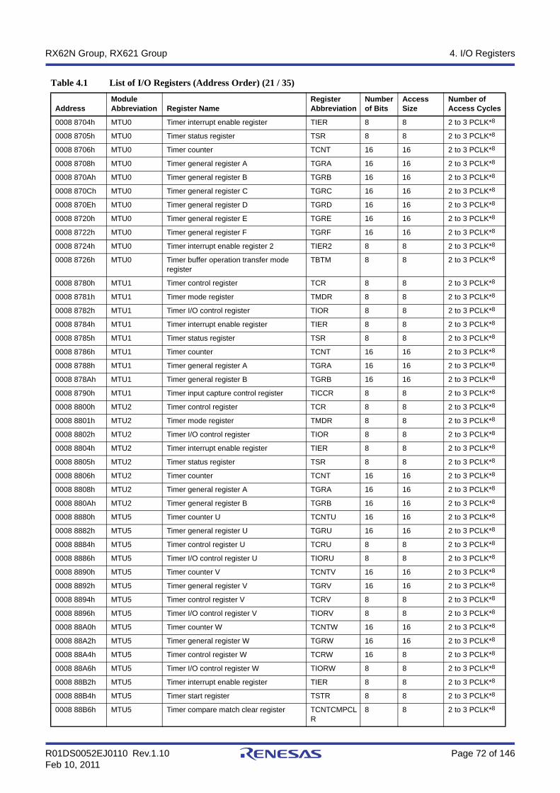
R01DS0052EJ0110 Rev.1.10 Page 72 of 146Feb 10, 2011
RX62N Group, RX621 Group 4. I/O Registers
0008 8704h MTU0 Timer interrupt enable register TIER 8 8 2 to 3 PCLK*8
0008 8705h MTU0 Timer status register TSR 8 8 2 to 3 PCLK*8
0008 8706h MTU0 Timer counter TCNT 16 16 2 to 3 PCLK*8
0008 8708h MTU0 Timer general register A TGRA 16 16 2 to 3 PCLK*8
0008 870Ah MTU0 Timer general register B TGRB 16 16 2 to 3 PCLK*8
0008 870Ch MTU0 Timer general register C TGRC 16 16 2 to 3 PCLK*8
0008 870Eh MTU0 Timer general register D TGRD 16 16 2 to 3 PCLK*8
0008 8720h MTU0 Timer general register E TGRE 16 16 2 to 3 PCLK*8
0008 8722h MTU0 Timer general register F TGRF 16 16 2 to 3 PCLK*8
0008 8724h MTU0 Timer interrupt enable register 2 TIER2 8 8 2 to 3 PCLK*8
0008 8726h MTU0 Timer buffer operation transfer mode register
TBTM 8 8 2 to 3 PCLK*8
0008 8780h MTU1 Timer control register TCR 8 8 2 to 3 PCLK*8
0008 8781h MTU1 Timer mode register TMDR 8 8 2 to 3 PCLK*8
0008 8782h MTU1 Timer I/O control register TIOR 8 8 2 to 3 PCLK*8
0008 8784h MTU1 Timer interrupt enable register TIER 8 8 2 to 3 PCLK*8
0008 8785h MTU1 Timer status register TSR 8 8 2 to 3 PCLK*8
0008 8786h MTU1 Timer counter TCNT 16 16 2 to 3 PCLK*8
0008 8788h MTU1 Timer general register A TGRA 16 16 2 to 3 PCLK*8
0008 878Ah MTU1 Timer general register B TGRB 16 16 2 to 3 PCLK*8
0008 8790h MTU1 Timer input capture control register TICCR 8 8 2 to 3 PCLK*8
0008 8800h MTU2 Timer control register TCR 8 8 2 to 3 PCLK*8
0008 8801h MTU2 Timer mode register TMDR 8 8 2 to 3 PCLK*8
0008 8802h MTU2 Timer I/O control register TIOR 8 8 2 to 3 PCLK*8
0008 8804h MTU2 Timer interrupt enable register TIER 8 8 2 to 3 PCLK*8
0008 8805h MTU2 Timer status register TSR 8 8 2 to 3 PCLK*8
0008 8806h MTU2 Timer counter TCNT 16 16 2 to 3 PCLK*8
0008 8808h MTU2 Timer general register A TGRA 16 16 2 to 3 PCLK*8
0008 880Ah MTU2 Timer general register B TGRB 16 16 2 to 3 PCLK*8
0008 8880h MTU5 Timer counter U TCNTU 16 16 2 to 3 PCLK*8
0008 8882h MTU5 Timer general register U TGRU 16 16 2 to 3 PCLK*8
0008 8884h MTU5 Timer control register U TCRU 8 8 2 to 3 PCLK*8
0008 8886h MTU5 Timer I/O control register U TIORU 8 8 2 to 3 PCLK*8
0008 8890h MTU5 Timer counter V TCNTV 16 16 2 to 3 PCLK*8
0008 8892h MTU5 Timer general register V TGRV 16 16 2 to 3 PCLK*8
0008 8894h MTU5 Timer control register V TCRV 8 8 2 to 3 PCLK*8
0008 8896h MTU5 Timer I/O control register V TIORV 8 8 2 to 3 PCLK*8
0008 88A0h MTU5 Timer counter W TCNTW 16 16 2 to 3 PCLK*8
0008 88A2h MTU5 Timer general register W TGRW 16 16 2 to 3 PCLK*8
0008 88A4h MTU5 Timer control register W TCRW 16 8 2 to 3 PCLK*8
0008 88A6h MTU5 Timer I/O control register W TIORW 8 8 2 to 3 PCLK*8
0008 88B2h MTU5 Timer interrupt enable register TIER 8 8 2 to 3 PCLK*8
0008 88B4h MTU5 Timer start register TSTR 8 8 2 to 3 PCLK*8
0008 88B6h MTU5 Timer compare match clear register TCNTCMPCLR
8 8 2 to 3 PCLK*8
Table 4.1 List of I/O Registers (Address Order) (21 / 35)
AddressModule Abbreviation Register Name
Register Abbreviation
Number of Bits
AccessSize
Number of Access Cycles

R01DS0052EJ0110 Rev.1.10 Page 73 of 146Feb 10, 2011
RX62N Group, RX621 Group 4. I/O Registers
0008 8900h POE Input level control/status register 1 ICSR1 16 16 2 to 3 PCLK*8
0008 8902h POE Output level control/status register 1 OCSR1 16 16 2 to 3 PCLK*8
0008 8904h POE Input level control/status register 2 ICSR2 16 16 2 to 3 PCLK*8
0008 8906h POE Output level control/status register 2 OCSR2 16 16 2 to 3 PCLK*8
0008 8908h POE Input level control/status register 3 ICSR3 16 16 2 to 3 PCLK*8
0008 890Ah POE Software port output enable register SPOER 8 8 2 to 3 PCLK*8
0008 890Bh POE Port output enable control register 1 POECR1 8 8 2 to 3 PCLK*8
0008 890Ch POE Port output enable control register 2 POECR2 16 16 2 to 3 PCLK*8
0008 890Eh POE Input level control/status register 4 ICSR4 16 16 2 to 3 PCLK*8
0008 8A00h MTU9 Timer control register TCR 8 8 2 to 3 PCLK*8
0008 8A01h MTU10 Timer control register TCR 8 8 2 to 3 PCLK*8
0008 8A02h MTU9 Timer mode register TMDR 8 8 2 to 3 PCLK*8
0008 8A03h MTU10 Timer mode register TMDR 8 8 2 to 3 PCLK*8
0008 8A04h MTU9 Timer I/O control register H TIORH 8 8 2 to 3 PCLK*8
0008 8A05h MTU9 Timer I/O control register L TIORL 8 8 2 to 3 PCLK*8
0008 8A06h MTU10 Timer I/O control register H TIORH 8 8 2 to 3 PCLK*8
0008 8A07h MTU10 Timer I/O control register L TIORL 8 8 2 to 3 PCLK*8
0008 8A08h MTU9 Timer interrupt enable register TIER 8 8 2 to 3 PCLK*8
0008 8A09h MTU10 Timer interrupt enable register TIER 8 8 2 to 3 PCLK*8
0008 8A0Ah MTUB Timer output master enable register TOER 8 8 2 to 3 PCLK*8
0008 8A0Dh MTUB Timer gate control register TGCR 8 8 2 to 3 PCLK*8
0008 8A0Eh MTUB Timer output control register 1 TOCR1 8 8 2 to 3 PCLK*8
0008 8A0Fh MTUB Timer output control register 2 TOCR2 8 8 2 to 3 PCLK*8
0008 8A10h MTU9 Timer counter TCNT 16 16 2 to 3 PCLK*8
0008 8A12h MTU10 Timer counter TCNT 16 16 2 to 3 PCLK*8
0008 8A14h MTUB Timer cycle data register TCDR 16 16 2 to 3 PCLK*8
0008 8A16h MTUB Timer dead time data register TDDR 16 16 2 to 3 PCLK*8
0008 8A18h MTU9 Timer general register A TGRA 16 16 2 to 3 PCLK*8
0008 8A1Ah MTU9 Timer general register B TGRB 16 16 2 to 3 PCLK*8
0008 8A1Ch MTU10 Timer general register A TGRA 16 16 2 to 3 PCLK*8
0008 8A1Eh MTU10 Timer general register B TGRB 16 16 2 to 3 PCLK*8
0008 8A20h MTUB Timer subcounter TCNTS 16 16 2 to 3 PCLK*8
0008 8A22h MTUB MTUB Timer cycle buffer register TCBR 16 16 2 to 3 PCLK*8
0008 8A24h MTU9 Timer general register C TGRC 16 16 2 to 3 PCLK*8
0008 8A26h MTU9 Timer general register D TGRD 16 16 2 to 3 PCLK*8
0008 8A28h MTU10 Timer general register C TGRC 16 16 2 to 3 PCLK*8
0008 8A2Ah MTU10 Timer general register D TGRD 16 16 2 to 3 PCLK*8
0008 8A2Ch MTU9 Timer status register TSR 8 8 2 to 3 PCLK*8
0008 8A2Dh MTU10 Timer status register TSR 8 8 2 to 3 PCLK*8
0008 8A30h MTUB Timer interrupt skipping set register TITCR 8 8 2 to 3 PCLK*8
0008 8A31h MTUB Timer interrupt skipping counter TITCNT 8 8 2 to 3 PCLK*8
0008 8A32h MTUB TUB Timer dead time enable register TBTER 8 8 2 to 3 PCLK*8
0008 8A34h MTUB Timer dead time enable register TDER 8 8 2 to 3 PCLK*8
0008 8A36h MTUB Timer output level buffer register TOLBR 8 8 2 to 3 PCLK*8
Table 4.1 List of I/O Registers (Address Order) (22 / 35)
AddressModule Abbreviation Register Name
Register Abbreviation
Number of Bits
AccessSize
Number of Access Cycles
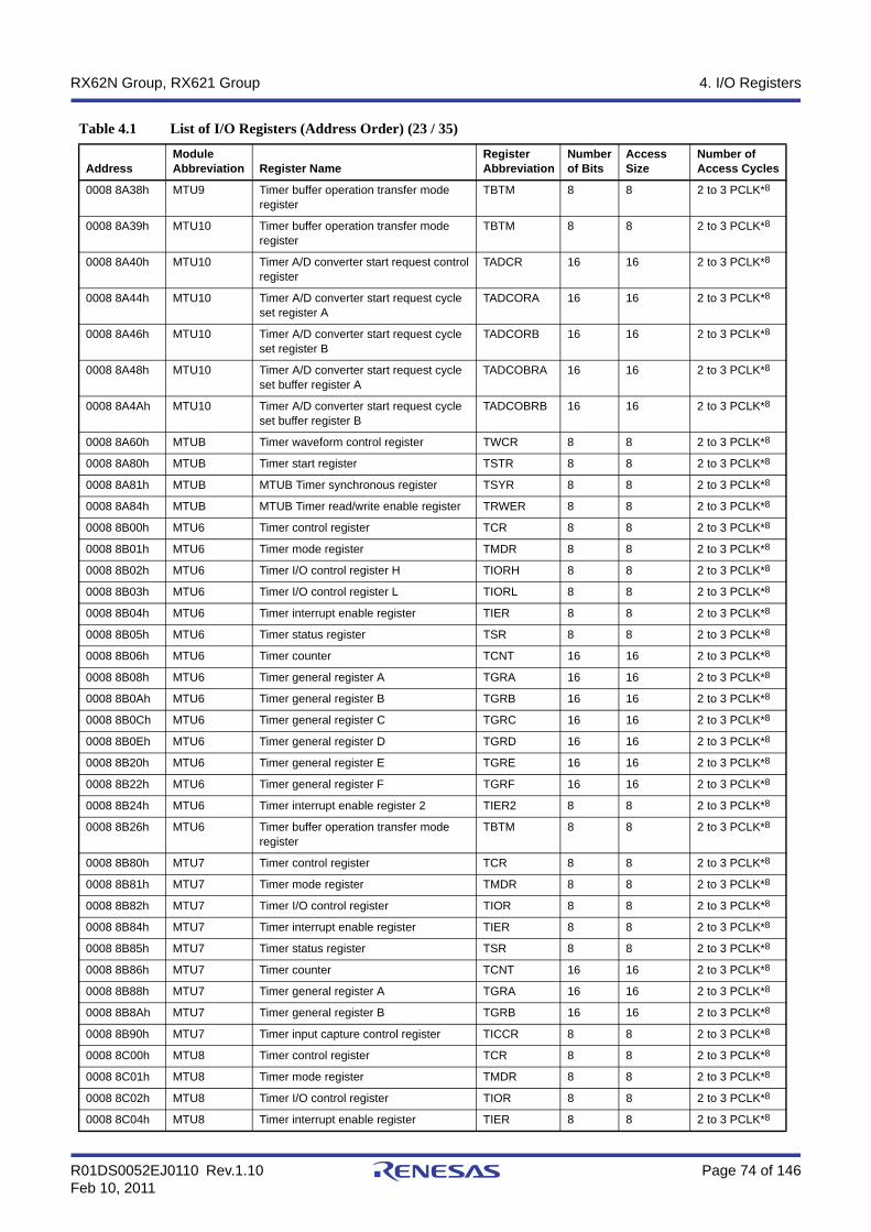
R01DS0052EJ0110 Rev.1.10 Page 74 of 146Feb 10, 2011
RX62N Group, RX621 Group 4. I/O Registers
0008 8A38h MTU9 Timer buffer operation transfer mode register
TBTM 8 8 2 to 3 PCLK*8
0008 8A39h MTU10 Timer buffer operation transfer mode register
TBTM 8 8 2 to 3 PCLK*8
0008 8A40h MTU10 Timer A/D converter start request control register
TADCR 16 16 2 to 3 PCLK*8
0008 8A44h MTU10 Timer A/D converter start request cycle set register A
TADCORA 16 16 2 to 3 PCLK*8
0008 8A46h MTU10 Timer A/D converter start request cycle set register B
TADCORB 16 16 2 to 3 PCLK*8
0008 8A48h MTU10 Timer A/D converter start request cycle set buffer register A
TADCOBRA 16 16 2 to 3 PCLK*8
0008 8A4Ah MTU10 Timer A/D converter start request cycle set buffer register B
TADCOBRB 16 16 2 to 3 PCLK*8
0008 8A60h MTUB Timer waveform control register TWCR 8 8 2 to 3 PCLK*8
0008 8A80h MTUB Timer start register TSTR 8 8 2 to 3 PCLK*8
0008 8A81h MTUB MTUB Timer synchronous register TSYR 8 8 2 to 3 PCLK*8
0008 8A84h MTUB MTUB Timer read/write enable register TRWER 8 8 2 to 3 PCLK*8
0008 8B00h MTU6 Timer control register TCR 8 8 2 to 3 PCLK*8
0008 8B01h MTU6 Timer mode register TMDR 8 8 2 to 3 PCLK*8
0008 8B02h MTU6 Timer I/O control register H TIORH 8 8 2 to 3 PCLK*8
0008 8B03h MTU6 Timer I/O control register L TIORL 8 8 2 to 3 PCLK*8
0008 8B04h MTU6 Timer interrupt enable register TIER 8 8 2 to 3 PCLK*8
0008 8B05h MTU6 Timer status register TSR 8 8 2 to 3 PCLK*8
0008 8B06h MTU6 Timer counter TCNT 16 16 2 to 3 PCLK*8
0008 8B08h MTU6 Timer general register A TGRA 16 16 2 to 3 PCLK*8
0008 8B0Ah MTU6 Timer general register B TGRB 16 16 2 to 3 PCLK*8
0008 8B0Ch MTU6 Timer general register C TGRC 16 16 2 to 3 PCLK*8
0008 8B0Eh MTU6 Timer general register D TGRD 16 16 2 to 3 PCLK*8
0008 8B20h MTU6 Timer general register E TGRE 16 16 2 to 3 PCLK*8
0008 8B22h MTU6 Timer general register F TGRF 16 16 2 to 3 PCLK*8
0008 8B24h MTU6 Timer interrupt enable register 2 TIER2 8 8 2 to 3 PCLK*8
0008 8B26h MTU6 Timer buffer operation transfer mode register
TBTM 8 8 2 to 3 PCLK*8
0008 8B80h MTU7 Timer control register TCR 8 8 2 to 3 PCLK*8
0008 8B81h MTU7 Timer mode register TMDR 8 8 2 to 3 PCLK*8
0008 8B82h MTU7 Timer I/O control register TIOR 8 8 2 to 3 PCLK*8
0008 8B84h MTU7 Timer interrupt enable register TIER 8 8 2 to 3 PCLK*8
0008 8B85h MTU7 Timer status register TSR 8 8 2 to 3 PCLK*8
0008 8B86h MTU7 Timer counter TCNT 16 16 2 to 3 PCLK*8
0008 8B88h MTU7 Timer general register A TGRA 16 16 2 to 3 PCLK*8
0008 8B8Ah MTU7 Timer general register B TGRB 16 16 2 to 3 PCLK*8
0008 8B90h MTU7 Timer input capture control register TICCR 8 8 2 to 3 PCLK*8
0008 8C00h MTU8 Timer control register TCR 8 8 2 to 3 PCLK*8
0008 8C01h MTU8 Timer mode register TMDR 8 8 2 to 3 PCLK*8
0008 8C02h MTU8 Timer I/O control register TIOR 8 8 2 to 3 PCLK*8
0008 8C04h MTU8 Timer interrupt enable register TIER 8 8 2 to 3 PCLK*8
Table 4.1 List of I/O Registers (Address Order) (23 / 35)
AddressModule Abbreviation Register Name
Register Abbreviation
Number of Bits
AccessSize
Number of Access Cycles

R01DS0052EJ0110 Rev.1.10 Page 75 of 146Feb 10, 2011
RX62N Group, RX621 Group 4. I/O Registers
0008 8C05h MTU8 Timer status register TSR 8 8 2 to 3 PCLK*8
0008 8C06h MTU8 Timer counter TCNT 16 16 2 to 3 PCLK*8
0008 8C08h MTU8 Timer general register A TGRA 16 16 2 to 3 PCLK*8
0008 8C0Ah MTU8 Timer general register B TGRB 16 16 2 to 3 PCLK*8
0008 8C80h MTU11 Timer counter U TCNTU 16 16 2 to 3 PCLK*8
0008 8C82h MTU11 Timer general register U TGRU 16 16 2 to 3 PCLK*8
0008 8C84h MTU11 Timer control register U TCRU 8 8 2 to 3 PCLK*8
0008 8C86h MTU11 Timer I/O control register U TIORU 8 8 2 to 3 PCLK*8
0008 8C90h MTU11 Timer counter V TCNTV 16 16 2 to 3 PCLK*8
0008 8C92h MTU11 Timer general register V TGRV 16 16 2 to 3 PCLK*8
0008 8C94h MTU11 Timer control register V TCRV 8 8 2 to 3 PCLK*8
0008 8C96h MTU11 Timer I/O control register V TIORV 8 8 2 to 3 PCLK*8
0008 8CA0h MTU11 Timer counter W TCNTW 16 16 2 to 3 PCLK*8
0008 8CA2h MTU11 Timer general register W TGRW 16 16 2 to 3 PCLK*8
0008 8CA4h MTU11 Timer control register W TCRW 8 8 2 to 3 PCLK*8
0008 8CA6h MTU11 Timer I/O control register W TIORW 8 8 2 to 3 PCLK*8
0008 8CB2h MTU11 Timer interrupt enable register TIER 8 8 2 to 3 PCLK*8
0008 8CB4h MTU11 Timer start register TSTR 8 8 2 to 3 PCLK*8
0008 8CB6h MTU11 Timer compare match clear register TCNTCMPCLR 8 8 2 to 3 PCLK*8
0008 9000h S12AD A/D control register ADCSR 8 8 2 to 3 PCLK*8
0008 9004h S12AD A/D channel select register ADANS 16 16 2 to 3 PCLK*8
0008 9008h S12AD A/D-converted value addition mode select register
ADADS 16 16 2 to 3 PCLK*8
0008 900Ch S12AD A/D-converted value addition count select register
ADADC 8 8 2 to 3 PCLK*8
0008 900Eh S12AD A/D control extended register ADCER 16 16 2 to 3 PCLK*8
0008 9010h S12AD A/D start trigger select register ADSTRGR 8 8 2 to 3 PCLK*8
0008 9020h S12AD A/D data register 0 ADDR0 16 16 2 to 3 PCLK*8
0008 9022h S12AD A/D data register 1 ADDR1 16 16 2 to 3 PCLK*8
0008 9024h S12AD A/D data register 2 ADDR2 16 16 2 to 3 PCLK*8
0008 9026h S12AD A/D data register 3 ADDR3 16 16 2 to 3 PCLK*8
0008 9028h S12AD A/D data register 4 ADDR4 16 16 2 to 3 PCLK*8
0008 902Ah S12AD A/D data register 5 ADDR5 16 16 2 to 3 PCLK*8
0008 902Ch S12AD A/D data register 6 ADDR6 16 16 2 to 3 PCLK*8
0008 902Eh S12AD A/D data register 7 ADDR7 16 16 2 to 3 PCLK*8
0008 C000h PORT0 Data direction register DDR 8 8 2 to 3 PCLK*8
0008 C001h PORT1 Data direction register DDR 8 8 2 to 3 PCLK*8
0008 C002h PORT2 Data direction register DDR 8 8 2 to 3 PCLK*8
0008 C003h PORT3 Data direction register DDR 8 8 2 to 3 PCLK*8
0008 C004h PORT4 Data direction register DDR 8 8 2 to 3 PCLK*8
0008 C005h PORT5 Data direction register DDR 8 8 2 to 3 PCLK*8
0008 C006h PORT6 Data direction register DDR*6*7 8 8 2 to 3 PCLK*8
0008 C007h PORT7 Data direction register DDR*6*7 8 8 2 to 3 PCLK*8
0008 C008h PORT8 Data direction register DDR*6*7 8 8 2 to 3 PCLK*8
0008 C009h PORT9 Data direction register DDR*6*7 8 8 2 to 3 PCLK*8
Table 4.1 List of I/O Registers (Address Order) (24 / 35)
AddressModule Abbreviation Register Name
Register Abbreviation
Number of Bits
AccessSize
Number of Access Cycles
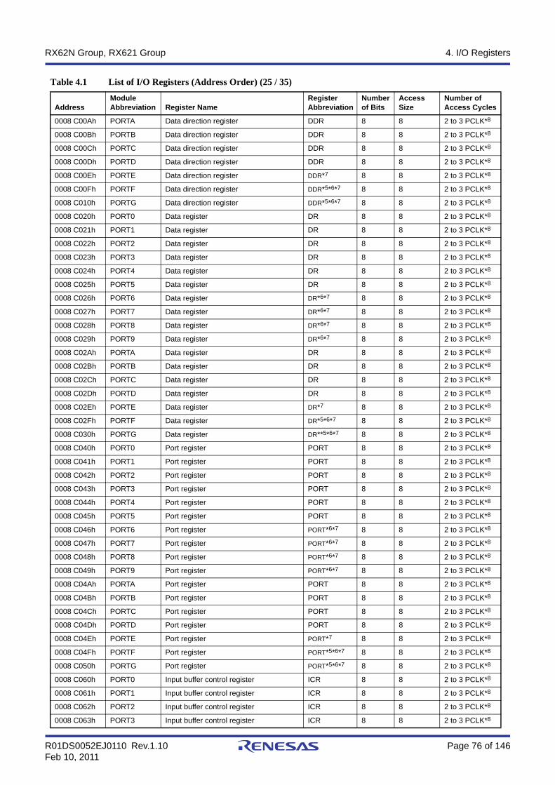
R01DS0052EJ0110 Rev.1.10 Page 76 of 146Feb 10, 2011
RX62N Group, RX621 Group 4. I/O Registers
0008 C00Ah PORTA Data direction register DDR 8 8 2 to 3 PCLK*8
0008 C00Bh PORTB Data direction register DDR 8 8 2 to 3 PCLK*8
0008 C00Ch PORTC Data direction register DDR 8 8 2 to 3 PCLK*8
0008 C00Dh PORTD Data direction register DDR 8 8 2 to 3 PCLK*8
0008 C00Eh PORTE Data direction register DDR*7 8 8 2 to 3 PCLK*8
0008 C00Fh PORTF Data direction register DDR*5*6*7 8 8 2 to 3 PCLK*8
0008 C010h PORTG Data direction register DDR*5*6*7 8 8 2 to 3 PCLK*8
0008 C020h PORT0 Data register DR 8 8 2 to 3 PCLK*8
0008 C021h PORT1 Data register DR 8 8 2 to 3 PCLK*8
0008 C022h PORT2 Data register DR 8 8 2 to 3 PCLK*8
0008 C023h PORT3 Data register DR 8 8 2 to 3 PCLK*8
0008 C024h PORT4 Data register DR 8 8 2 to 3 PCLK*8
0008 C025h PORT5 Data register DR 8 8 2 to 3 PCLK*8
0008 C026h PORT6 Data register DR*6*7 8 8 2 to 3 PCLK*8
0008 C027h PORT7 Data register DR*6*7 8 8 2 to 3 PCLK*8
0008 C028h PORT8 Data register DR*6*7 8 8 2 to 3 PCLK*8
0008 C029h PORT9 Data register DR*6*7 8 8 2 to 3 PCLK*8
0008 C02Ah PORTA Data register DR 8 8 2 to 3 PCLK*8
0008 C02Bh PORTB Data register DR 8 8 2 to 3 PCLK*8
0008 C02Ch PORTC Data register DR 8 8 2 to 3 PCLK*8
0008 C02Dh PORTD Data register DR 8 8 2 to 3 PCLK*8
0008 C02Eh PORTE Data register DR*7 8 8 2 to 3 PCLK*8
0008 C02Fh PORTF Data register DR*5*6*7 8 8 2 to 3 PCLK*8
0008 C030h PORTG Data register DR**5*6*7 8 8 2 to 3 PCLK*8
0008 C040h PORT0 Port register PORT 8 8 2 to 3 PCLK*8
0008 C041h PORT1 Port register PORT 8 8 2 to 3 PCLK*8
0008 C042h PORT2 Port register PORT 8 8 2 to 3 PCLK*8
0008 C043h PORT3 Port register PORT 8 8 2 to 3 PCLK*8
0008 C044h PORT4 Port register PORT 8 8 2 to 3 PCLK*8
0008 C045h PORT5 Port register PORT 8 8 2 to 3 PCLK*8
0008 C046h PORT6 Port register PORT*6*7 8 8 2 to 3 PCLK*8
0008 C047h PORT7 Port register PORT*6*7 8 8 2 to 3 PCLK*8
0008 C048h PORT8 Port register PORT*6*7 8 8 2 to 3 PCLK*8
0008 C049h PORT9 Port register PORT*6*7 8 8 2 to 3 PCLK*8
0008 C04Ah PORTA Port register PORT 8 8 2 to 3 PCLK*8
0008 C04Bh PORTB Port register PORT 8 8 2 to 3 PCLK*8
0008 C04Ch PORTC Port register PORT 8 8 2 to 3 PCLK*8
0008 C04Dh PORTD Port register PORT 8 8 2 to 3 PCLK*8
0008 C04Eh PORTE Port register PORT*7 8 8 2 to 3 PCLK*8
0008 C04Fh PORTF Port register PORT*5*6*7 8 8 2 to 3 PCLK*8
0008 C050h PORTG Port register PORT*5*6*7 8 8 2 to 3 PCLK*8
0008 C060h PORT0 Input buffer control register ICR 8 8 2 to 3 PCLK*8
0008 C061h PORT1 Input buffer control register ICR 8 8 2 to 3 PCLK*8
0008 C062h PORT2 Input buffer control register ICR 8 8 2 to 3 PCLK*8
0008 C063h PORT3 Input buffer control register ICR 8 8 2 to 3 PCLK*8
Table 4.1 List of I/O Registers (Address Order) (25 / 35)
AddressModule Abbreviation Register Name
Register Abbreviation
Number of Bits
AccessSize
Number of Access Cycles

R01DS0052EJ0110 Rev.1.10 Page 77 of 146Feb 10, 2011
RX62N Group, RX621 Group 4. I/O Registers
0008 C064h PORT4 Input buffer control register ICR 8 8 2 to 3 PCLK*8
0008 C065h PORT5 Input buffer control register ICR 8 8 2 to 3 PCLK*8
0008 C066h PORT6 Input buffer control register ICR*6*7 8 8 2 to 3 PCLK*8
0008 C067h PORT7 Input buffer control register ICR*6*7 8 8 2 to 3 PCLK*8
0008 C068h PORT8 Input buffer control register ICR*6*7 8 8 2 to 3 PCLK*8
0008 C069h PORT9 Input buffer control register ICR*6*7 8 8 2 to 3 PCLK*8
0008 C06Ah PORTA Input buffer control register ICR 8 8 2 to 3 PCLK*8
0008 C06Bh PORTB Input buffer control register ICR 8 8 2 to 3 PCLK*8
0008 C06Ch PORTC Input buffer control register ICR 8 8 2 to 3 PCLK*8
0008 C06Dh PORTD Input buffer control register ICR 8 8 2 to 3 PCLK*8
0008 C06Eh PORTE Input buffer control register ICR*7 8 8 2 to 3 PCLK*8
0008 C06Fh PORTF Input buffer control register ICR*5*6*7 8 8 2 to 3 PCLK*8
0008 C070h PORTG Input buffer control register ICR*5*6*7 8 8 2 to 3 PCLK*8
0008 C080h PORT0 Open drain control register ODR 8 8 2 to 3 PCLK*8
0008 C081h PORT1 Open drain control register ODR 8 8 2 to 3 PCLK*8
0008 C082h PORT2 Open drain control register ODR 8 8 2 to 3 PCLK*8
0008 C083h PORT3 Open drain control register ODR 8 8 2 to 3 PCLK*8
0008 C08Ch PORTC Open drain control register ODR 8 8 2 to 3 PCLK*8
0008 C0C9h PORT9 Pull-up resistor control register PCR*6*7 8 8 2 to 3 PCLK*8
0008 C0CAh PORTA Pull-up resistor control register PCR 8 8 2 to 3 PCLK*8
0008 C0CBh PORTB Pull-up resistor control register PCR 8 8 2 to 3 PCLK*8
0008 C0CCh PORTC Pull-up resistor control register PCR 8 8 2 to 3 PCLK*8
0008 C0CDh PORTD Pull-up resistor control register PCR 8 8 2 to 3 PCLK*8
0008 C0CEh PORTE Pull-up resistor control register PCR*7 8 8 2 to 3 PCLK*8
0008 C0D0h PORTG Pull-up resistor control register PCR*5*6*7 8 8 2 to 3 PCLK*8
0008 C100h IOPORT Port function register 0 PF0CSE 8 8 2 to 3 PCLK*8
0008 C101h IOPORT Port function register 1 PF1CSS*6*7 8 8 2 to 3 PCLK*8
0008 C102h IOPORT Port function register 2 PF2CSS*6*7 8 8 2 to 3 PCLK*8
0008 C103h IOPORT Port function register 3 PF3BUS 8 8 2 to 3 PCLK*8
0008 C104h IOPORT Port function register 4 PF4BUS 8 8 2 to 3 PCLK*8
0008 C105h IOPORT Port function register 5 PF5BUS 8 8 2 to 3 PCLK*8
0008 C106h IOPORT Port function register 6 PF6BUS 8 8 2 to 3 PCLK*8
0008 C107h IOPORT Port function register 7 PF7DMA 8 8 2 to 3 PCLK*8
0008 C108h IOPORT Port function register 8 PF8IRQ 8 8 2 to 3 PCLK*8
0008 C109h IOPORT Port function register 9 PF9IRQ 8 8 2 to 3 PCLK*8
0008 C10Ah IOPORT Port function register A PFAADC 8 8 2 to 3 PCLK*8
0008 C10Bh IOPORT Port function register B PFBTMR 8 8 2 to 3 PCLK*8
0008 C10Ch IOPORT Port function register C PFCMTU 8 8 2 to 3 PCLK*8
0008 C10Dh IOPORT Port function register D PFDMTU 8 8 2 to 3 PCLK*8
0008 C10Eh IOPORT Port function register E PFENET 8 8 2 to 3 PCLK*8
0008 C10Fh IOPORT Port function register F PFFSCI 8 8 2 to 3 PCLK*8
0008 C110h IOPORT Port function register G PFGSPI 8 8 2 to 3 PCLK*8
0008 C111h IOPORT Port function register H PFHSPI 8 8 2 to 3 PCLK*8
0008 C113h IOPORT Port function register J PFJCAN 8 8 2 to 3 PCLK*8
0008 C114h IOPORT Port function register K PFKUSB 8 8 2 to 3 PCLK*8
Table 4.1 List of I/O Registers (Address Order) (26 / 35)
AddressModule Abbreviation Register Name
Register Abbreviation
Number of Bits
AccessSize
Number of Access Cycles

R01DS0052EJ0110 Rev.1.10 Page 78 of 146Feb 10, 2011
RX62N Group, RX621 Group 4. I/O Registers
0008 C115h IOPORT Port function register L PFLUSB*6*7 8 8 2 to 3 PCLK*8
0008 C116h IOPORT Port function register M PFMPOE*7 8 8 2 to 3 PCLK*8
0008 C117h IOPORT Port function register N PFNPOE*7 8 8 2 to 3 PCLK*8
0008 C280h SYSTEM Deep standby control register DPSBYCR 8 8 4 to 5 PCLK*8
0008 C281h SYSTEM Deep standby wait control register DPSWCR 8 8 4 to 5 PCLK*8
0008 C282h SYSTEM Deep standby interrupt enable register DPSIER 8 8 4 to 5 PCLK*8
0008 C283h SYSTEM Deep standby interrupt flag register DPSIFR 8 8 4 to 5 PCLK*8
0008 C284h SYSTEM Deep standby interrupt edge register DPSIEGR 8 8 4 to 5 PCLK*8
0008 C285h SYSTEM Reset status register RSTSR 8 8 4 to 5 PCLK*8
0008 C289h FLASH Flash write erase protection register FWEPROR 8 8 4 to 5 PCLK*8
0008 C28Ah SYSTEM Sub-clock oscillator control register SUBOSCCR 8 8 4 to 5 PCLK*8
0008 C28C SYSTEM Key code register for voltage detection control register
LVDKEYR 8 8 4 to 5 PCLK*8
0008 C28Dh SYSTEM Voltage detection control register LVDCR 8 8 4 to 5 PCLK*8
0008 C290h SYSTEM Deep standby backup register 0 DPSBKR0 8 8 4 to 5 PCLK*8
0008 C291h SYSTEM Deep standby backup register 1 DPSBKR1 8 8 4 to 5 PCLK*8
0008 C292h SYSTEM Deep standby backup register 2 DPSBKR2 8 8 4 to 5 PCLK*8
0008 C293h SYSTEM Deep standby backup register 3 DPSBKR3 8 8 4 to 5 PCLK*8
0008 C294h SYSTEM Deep standby backup register 4 DPSBKR4 8 8 4 to 5 PCLK*8
0008 C295h SYSTEM Deep standby backup register 5 DPSBKR5 8 8 4 to 5 PCLK*8
0008 C296h SYSTEM Deep standby backup register 6 DPSBKR6 8 8 4 to 5 PCLK*8
0008 C297h SYSTEM Deep standby backup register 7 DPSBKR7 8 8 4 to 5 PCLK*8
0008 C298h SYSTEM Deep standby backup register 8 DPSBKR8 8 8 4 to 5 PCLK*8
0008 C299h SYSTEM Deep standby backup register 9 DPSBKR9 8 8 4 to 5 PCLK*8
0008 C29Ah SYSTEM Deep standby backup register 10 DPSBKR10 8 8 4 to 5 PCLK*8
0008 C29Bh SYSTEM Deep standby backup register 11 DPSBKR11 8 8 4 to 5 PCLK*8
0008 C29Ch SYSTEM Deep standby backup register 12 DPSBKR12 8 8 4 to 5 PCLK*8
0008 C29Dh SYSTEM Deep standby backup register 13 DPSBKR13 8 8 4 to 5 PCLK*8
0008 C29Eh SYSTEM Deep standby backup register 14 DPSBKR14 8 8 4 to 5 PCLK*8
0008 C29Fh SYSTEM Deep standby backup register 15 DPSBKR15 8 8 4 to 5 PCLK*8
0008 C2A0h SYSTEM Deep standby backup register 16 DPSBKR16 8 8 4 to 5 PCLK*8
0008 C2A1h SYSTEM Deep standby backup register 17 DPSBKR17 8 8 4 to 5 PCLK*8
0008 C2A2h SYSTEM Deep standby backup register 18 DPSBKR18 8 8 4 to 5 PCLK*8
0008 C2A3h SYSTEM Deep standby backup register 19 DPSBKR19 8 8 4 to 5 PCLK*8
0008 C2A4h SYSTEM Deep standby backup register 20 DPSBKR20 8 8 4 to 5 PCLK*8
0008 C2A5h SYSTEM Deep standby backup register 21 DPSBKR21 8 8 4 to 5 PCLK*8
0008 C2A6h SYSTEM Deep standby backup register 22 DPSBKR22 8 8 4 to 5 PCLK*8
0008 C2A7h SYSTEM Deep standby backup register 23 DPSBKR23 8 8 4 to 5 PCLK*8
0008 C2A8h SYSTEM Deep standby backup register 24 DPSBKR24 8 8 4 to 5 PCLK*8
0008 C2A9h SYSTEM Deep standby backup register 25 DPSBKR25 8 8 4 to 5 PCLK*8
0008 C2AAh SYSTEM Deep standby backup register 26 DPSBKR26 8 8 4 to 5 PCLK*8
0008 C2ABh SYSTEM Deep standby backup register 27 DPSBKR27 8 8 4 to 5 PCLK*8
0008 C2ACh SYSTEM Deep standby backup register 28 DPSBKR28 8 8 4 to 5 PCLK*8
0008 C2ADh SYSTEM Deep standby backup register 29 DPSBKR29 8 8 4 to 5 PCLK*8
0008 C2AEh SYSTEM Deep standby backup register 30 DPSBKR30 8 8 4 to 5 PCLK*8
Table 4.1 List of I/O Registers (Address Order) (27 / 35)
AddressModule Abbreviation Register Name
Register Abbreviation
Number of Bits
AccessSize
Number of Access Cycles

R01DS0052EJ0110 Rev.1.10 Page 79 of 146Feb 10, 2011
RX62N Group, RX621 Group 4. I/O Registers
0008 C2AFh SYSTEM Deep standby backup register 31 DPSBKR31 8 8 4 to 5 PCLK*8
0008 C400h RTC 64-Hz counter R64CNT 8 8 2 to 3 PCLK*8
0008 C402h RTC Second counter RSECCNT 8 8 2 to 3 PCLK*8
0008 C404h RTC Minute counter RMINCNT 8 8 2 to 3 PCLK*8
0008 C406h RTC Hour counter RHRCNT 8 8 2 to 3 PCLK*8
0008 C408h RTC Day-of-week counter RWKCNT 8 8 2 to 3 PCLK*8
0008 C40Ah RTC Date counter RDAYCNT 8 8 2 to 3 PCLK*8
0008 C40Ch RTC Month counter RMONCNT 8 8 2 to 3 PCLK*8
0008 C40Eh RTC Year counter RYRCNT 16 16 2 to 3 PCLK*8
0008 C410h RTC Second alarm register RSECAR 8 8 2 to 3 PCLK*8
0008 C412h RTC Minute alarm register RMINAR 8 8 2 to 3 PCLK*8
0008 C414h RTC Hour alarm register RHRAR 8 8 2 to 3 PCLK*8
0008 C416h RTC Day-of-week alarm register RWKAR 8 8 2 to 3 PCLK*8
0008 C418h RTC Date alarm register RDAYAR 8 8 2 to 3 PCLK*8
0008 C41Ah RTC Month alarm register RMONAR 8 8 2 to 3 PCLK*8
0008 C41Ch RTC Year alarm register RYRAR 16 16 2 to 3 PCLK*8
0008 C41Eh RTC Year alarm enable register RYRAREN 8 8 2 to 3 PCLK*8
0008 C422h RTC RTC control register 1 RCR1 8 8 2 to 3 PCLK*8
0008 C424h RTC RTC control register 2 RCR2 8 8 2 to 3 PCLK*8
0009 0200h to 0009 03FFh
CAN0 Mailbox registers 0 to 31 MB0 to MB031
128 8, 16, 32 2 to 3 PCLK*8
0009 0400h CAN0 Mask register 0 MKR0 32 8, 16, 32 2 to 3 PCLK*8
0009 0404h CAN0 Mask register 1 MKR1 32 8, 16, 32 2 to 3 PCLK*8
0009 0408h CAN0 Mask register 2 MKR2 32 8, 16, 32 2 to 3 PCLK*8
0009 040Ch CAN0 Mask register 3 MKR3 32 8, 16, 32 2 to 3 PCLK*8
0009 0410h CAN0 Mask register 4 MKR4 32 8, 16, 32 2 to 3 PCLK*8
0009 0414h CAN0 Mask register 5 MKR5 32 8, 16, 32 2 to 3 PCLK*8
0009 0418h CAN0 Mask register 6 MKR6 32 8, 16, 32 2 to 3 PCLK*8
0009 041Ch CAN0 Mask register 7 MKR7 32 8, 16, 32 2 to 3 PCLK*8
0009 0420h CAN0 FIFO received ID compare register 0 FIDCR0 32 8, 16, 32 2 to 3 PCLK*8
0009 0424h CAN0 FIFO received ID compare register 1 FIDCR1 32 8, 16, 32 2 to 3 PCLK*8
0009 0428h CAN0 Mask invalid register MKIVLR 32 8, 16, 32 2 to 3 PCLK*8
0009 042Ch CAN0 Mailbox interrupt enable register MIER 32 8, 16, 32 2 to 3 PCLK*8
0009 0820h to 0009 083Fh
CAN0 Message control registers 0 to 31 C0MCTL0 to C0MCTL031
8 8 2 to 3 PCLK*8
0009 0840h CAN0 Control register CTLR 16 8, 16 2 to 3 PCLK*8
0009 0842h CAN0 Status register STR 16 8, 16 2 to 3 PCLK*8
0009 0844h CAN0 Bit configuration register BCR 32 8, 16, 32 2 to 3 PCLK*8
0009 0848h CAN0 Receive FIFO control register RFCR 8 8 2 to 3 PCLK*8
0009 0849h CAN0 Receive FIFO pointer control register RFPCR 8 8 2 to 3 PCLK*8
0009 084Ah CAN0 Transmit FIFO control register TFCR 8 8 2 to 3 PCLK*8
0009 084Bh CAN0 Transmit FIFO pointer control register TFPCR 8 8 2 to 3 PCLK*8
0009 084Ch CAN0 Error interrupt enable register EIER 8 8 2 to 3 PCLK*8
0009 084Dh CAN0 Error interrupt factor judge register EIFR 8 8 2 to 3 PCLK*8
0009 084Eh CAN0 Receive error count register RECR 8 8 2 to 3 PCLK*8
Table 4.1 List of I/O Registers (Address Order) (28 / 35)
AddressModule Abbreviation Register Name
Register Abbreviation
Number of Bits
AccessSize
Number of Access Cycles

R01DS0052EJ0110 Rev.1.10 Page 80 of 146Feb 10, 2011
RX62N Group, RX621 Group 4. I/O Registers
0009 084Fh CAN0 Transmit error count register TECR 8 8 2 to 3 PCLK*8
0009 0850h CAN0 Error code store register ECSR 8 8 2 to 3 PCLK*8
0009 0851h CAN0 Channel search support register CSSR 8 8 2 to 3 PCLK*8
0009 0852h CAN0 Mailbox search status registe MSSR 8 8 2 to 3 PCLK*8
0009 0853h CAN0 Mailbox search mode registe MSMR 8 8 2 to 3 PCLK*8
0009 0854h CAN0 Time stamp registerr TSR 16 8, 16 2 to 3 PCLK*8
0009 0856h CAN0 Acceptance filter support register AFSR 16 8, 16 2 to 3 PCLK*8
0009 0858h CAN0 Test control register TCR 8 8 2 to 3 PCLK*8
000A 0000h USB0 System configuration control register SYSCFG 16 16 3 to 4 PCLK*8
000A 0004h USB0 System configuration status register 0 SYSSTS0 16 16 at least 9 PCLK*9
000A 0008h USB0 Device state control register 0 DVSTCTR0 16 16 at least 9 PCLK*9
000A 0014h USB0 CFIFO port register CFIFO 16 8, 16 3 to 4 PCLK*8
000A 0018h USB0 D0FIFO port register D0FIFO 16 8, 16 3 to 4 PCLK*8
000A 001Ch USB0 D1FIFO port register D1FIFO 16 8, 16 3 to 4 PCLK*8
000A 0020h USB0 CFIFO port select register CFIFOSEL 16 16 3 to 4 PCLK*8
000A 0022h USB0 CFIFO port control register CFIFOCTR 16 16 3 to 4 PCLK*8
000A 0028h USB0 D0FIFO port select register D0FIFOSEL 16 16 3 to 4 PCLK*8
000A 002Ah USB0 D0FIFO port control register D0FIFOCTR 16 16 3 to 4 PCLK*8
000A 002Ch USB0 D1FIFO port select register D1FIFOSEL 16 16 3 to 4 PCLK*8
000A 002Eh USB0 D1FIFO port control register D1FIFOCTR 16 16 3 to 4 PCLK*8
000A 0030h USB0 Interrupt enable register 0 INTENB0 16 16 at least 9 PCLK*9
000A 0032h USB0 Interrupt enable register 1 INTENB1 16 16 at least 9 PCLK*9
000A 0036h USB0 BRDY interrupt enable register BRDYENB 16 16 at least 9 PCLK*9
000A 0038h USB0 NRDY interrupt enable register NRDYENB 16 16 at least 9 PCLK*9
000A 003Ah USB0 BEMP interrupt enable register BEMPENB 16 16 at least 9 PCLK*9
000A 003Ch USB0 SOF output configuration register SOFCFG 16 16 at least 9 PCLK*9
000A 0040h USB0 Interrupt status register 0 INTSTS0 16 16 at least 9 PCLK*9
000A 0042h USB0 Interrupt status register 1 INTSTS1 16 16 at least 9 PCLK*9
000A 0046h USB0 BRDY interrupt enable register BRDYSTS 16 16 at least 9 PCLK*9
000A 0048h USB0 NRDY interrupt status register NRDYSTS 16 16 at least 9 PCLK*9
000A 004Ah USB0 BEMP interrupt status register BEMPSTS 16 16 at least 9 PCLK*9
000A 004Ch USB0 Frame number register FRMNUM 16 16 at least 9 PCLK*9
000A 004Eh USB0 Device state change register DVCHGR 16 16 at least 9 PCLK*9
000A 0050h USB0 USB address register USBADDR 16 16 at least 9 PCLK*9
Table 4.1 List of I/O Registers (Address Order) (29 / 35)
AddressModule Abbreviation Register Name
Register Abbreviation
Number of Bits
AccessSize
Number of Access Cycles

R01DS0052EJ0110 Rev.1.10 Page 81 of 146Feb 10, 2011
RX62N Group, RX621 Group 4. I/O Registers
000A 0054h USB0 USB request type register USBREQ 16 16 at least 9 PCLK*9
000A 0056h USB0 USB request value register USBVAL 16 16 at least 9 PCLK*9
000A 0058h USB0 USB request index register USBINDX 16 16 at least 9 PCLK*9
000A 005Ah USB0 USB request length register USBLENG 16 16 at least 9 PCLK*9
000A 005Ch USB0 DCP configuration register DCPCFG 16 16 at least 9 PCLK*9
000A 005Eh USB0 DCP maximum packet size register DCPMAXP 16 16 at least 9 PCLK*9
000A 0060h USB0 DCP control register DCPCTR 16 16 at least 9 PCLK*9
000A 0064h USB0 Pipe window select register PIPESEL 16 16 at least 9 PCLK*9
000A 0068h USB0 Pipe configuration register PIPECFG 16 16 at least 9 PCLK*9
000A 006Ch USB0 Pipe maximum packet size register PIPEMAXP 16 16 at least 9 PCLK*9
000A 006Eh USB0 Pipe cycle control register PIPEPERI 16 16 at least 9 PCLK*9
000A 0070h USB0 Pipe 1 control register PIPE1CTR 16 16 at least 9 PCLK*9
000A 0072h USB0 Pipe 2 control register PIPE2CTR 16 16 at least 9 PCLK*9
000A 0074h USB0 Pipe 3 control register PIPE3CTR 16 16 at least 9 PCLK*9
000A 0076h USB0 Pipe 4 control register PIPE4CTR 16 16 at least 9 PCLK*9
000A 0078h USB0 Pipe 5 control register PIPE5CTR 16 16 at least 9 PCLK*9
000A 007Ah USB0 Pipe 6 control register PIPE6CTR 16 16 at least 9 PCLK*9
000A 007Ch USB0 Pipe 7 control register PIPE7CTR 16 16 at least 9 PCLK*9
000A 007Eh USB0 Pipe 8 control register PIPE8CTR 16 16 at least 9 PCLK*9
000A 0080h USB0 Pipe 9 control register PIPE9CTR 16 16 at least 9 PCLK*9
000A 0090h USB0 Pipe 1 transaction counter enable register
PIPE1TRE 16 16 at least 9 PCLK*9
000A 0092h USB0 Pipe 1 transaction counter register PIPE1TRN 16 16 at least 9 PCLK*9
000A 0094h USB0 Pipe 2 transaction counter enable register
PIPE2TRE 16 16 at least 9 PCLK*9
000A 0096h USB0 Pipe 2 transaction counter register PIPE2TRN 16 16 at least 9 PCLK*9
000A 0098h USB0 Pipe 3 transaction counter enable register
PIPE3TRE 16 16 at least 9 PCLK*9
000A 009Ah USB0 Pipe 3 transaction counter register PIPE3TRN 16 16 at least 9 PCLK*9
Table 4.1 List of I/O Registers (Address Order) (30 / 35)
AddressModule Abbreviation Register Name
Register Abbreviation
Number of Bits
AccessSize
Number of Access Cycles

R01DS0052EJ0110 Rev.1.10 Page 82 of 146Feb 10, 2011
RX62N Group, RX621 Group 4. I/O Registers
000A 009Ch USB0 Pipe 4 transaction counter enable register
PIPE4TRE 16 16 at least 9 PCLK*9
000A 009Eh USB0 Pipe 4 transaction counter register PIPE4TRN 16 16 at least 9 PCLK*9
000A 00A0h USB0 Pipe 5 transaction counter enable register
PIPE5TRE 16 16 at least 9 PCLK*9
000A 00A2h USB0 Pipe 5 transaction counter register PIPE5TRN 16 16 at least 9 PCLK*9
000A 00D0h USB0 Device address 0 configuration register DEVADD0 16 16 at least 9 PCLK*9
000A 00D2h USB0 Device address 1 configuration register DEVADD1 16 16 at least 9 PCLK*9
000A 00D4h USB0 Device address 2 configuration register DEVADD2 16 16 at least 9 PCLK*9
000A 00D6h USB0 Device address 3 configuration register DEVADD3 16 16 at least 9 PCLK*9
000A 00D8h USB0 Device address 4 configuration register DEVADD4 16 16 at least 9 PCLK*9
000A 00DAh USB0 Device address 5 configuration register DEVADD5 16 16 at least 9 PCLK*9
000A 0200h USB1 System configuration control register SYSCFG 16 16 3 to 4 PCLK*8
000A 0204h USB1 System configuration status register 0 SYSSTS0 16 16 at least 9 PCLK*9
000A 0208h USB1 Device state control register 0 DVSTCTR0 16 16 at least 9 PCLK*9
000A 0214h USB1 CFIFO port register CFIFO 16 8, 16 3 to 4 PCLK*8
000A 0218h USB1 D0FIFO port register D0FIFO 16 8, 16 3 to 4 PCLK*8
000A 021Ch USB1 D1FIFO port register D1FIFO 16 8, 16 3 to 4 PCLK*8
000A 0220h USB1 CFIFO port select register CFIFOSEL 16 16 3 to 4 PCLK*8
000A 0222h USB1 CFIFO port control register CFIFOCTR 16 16 3 to 4 PCLK*8
000A 0228h USB1 D0FIFO port select register D0FIFOSEL 16 16 3 to 4 PCLK*8
000A 022Ah USB1 D0FIFO port control register D0FIFOCTR 16 16 3 to 4 PCLK*8
000A 022Ch USB1 D1FIFO port select register D1FIFOSEL 16 16 3 to 4 PCLK*8
000A 022Eh USB1 D1FIFO port control register D1FIFOCTR 16 16 3 to 4 PCLK*8
000A 0230h USB1 Interrupt enable register 0 INTENB0 16 16 at least 9 PCLK*9
000A 0232h USB1 Interrupt enable register 1 INTENB1 16 16 at least 9 PCLK*9
000A 0236h USB1 BRDY interrupt enable register BRDYENB 16 16 at least 9 PCLK*9
000A 0238h USB1 NRDY interrupt enable register NRDYENB 16 16 at least 9 PCLK*9
000A 023Ah USB1 BEMP interrupt enable register BEMPENB 16 16 at least 9 PCLK*9
000A 023Ch USB1 SOF output configuration register SOFCFG 16 16 at least 9 PCLK*9
000A 0240h USB1 Interrupt status register 0 INTSTS0 16 16 at least 9 PCLK*9
000A 0242h USB1 Interrupt status register 1 INTSTS1 16 16 at least 9 PCLK*9
Table 4.1 List of I/O Registers (Address Order) (31 / 35)
AddressModule Abbreviation Register Name
Register Abbreviation
Number of Bits
AccessSize
Number of Access Cycles

R01DS0052EJ0110 Rev.1.10 Page 83 of 146Feb 10, 2011
RX62N Group, RX621 Group 4. I/O Registers
000A 0246h USB1 BRDY interrupt status register BRDYSTS 16 16 at least 9 PCLK*9
000A 0248h USB1 NRDY interrupt status register NRDYSTS 16 16 at least 9 PCLK*9
000A 024Ah USB1 BEMP interrupt status register BEMPSTS 16 16 at least 9 PCLK*9
000A 024Ch USB1 Frame number register FRMNUM 16 16 at least 9 PCLK*9
000A 024Eh USB1 Device state change register DVCHGR 16 16 at least 9 PCLK*9
000A 0250h USB1 USB address register USBADDR 16 16 at least 9 PCLK*9
000A 0254h USB1 USB request type register USBREQ 16 16 at least 9 PCLK*9
000A 0256h USB1 USB request value register USBVAL 16 16 at least 9 PCLK*9
000A 0258h USB1 USB request index register USBINDX 16 16 at least 9 PCLK*9
000A 025Ah USB1 USB request length register USBLENG 16 16 at least 9 PCLK*9
000A 025Ch USB1 DCP configuration register DCPCFG 16 16 at least 9 PCLK*9
000A 025Eh USB1 DCP maximum packet size register DCPMAXP 16 16 at least 9 PCLK*9
000A 0260h USB1 DCP control register DCPCTR 16 16 at least 9 PCLK*9
000A 0264h USB1 Pipe window select register PIPESEL 16 16 at least 9 PCLK*9
000A 0268h USB1 Pipe configuration register PIPECFG 16 16 at least 9 PCLK*9
000A 026Ch USB1 Pipe maximum packet size register PIPEMAXP 16 16 at least 9 PCLK*9
000A 026Eh USB1 Pipe cycle control register PIPEPERI 16 16 at least 9 PCLK*9
000A 0270h USB1 Pipe 1 control register PIPE1CTR 16 16 at least 9 PCLK*9
000A 0272h USB1 Pipe 2 control register PIPE2CTR 16 16 at least 9 PCLK*9
000A 0274h USB1 Pipe 3 control register PIPE3CTR 16 16 at least 9 PCLK*9
000A 0276h USB1 Pipe 4 control register PIPE4CTR 16 16 at least 9 PCLK*9
000A 0278h USB1 Pipe 5 control register PIPE5CTR 16 16 at least 9 PCLK*9
000A 027Ah USB1 Pipe 6 control register PIPE6CTR 16 16 at least 9 PCLK*9
000A 027Ch USB1 Pipe 7 control register PIPE7CTR 16 16 at least 9 PCLK*9
000A 027Eh USB1 Pipe 8 control register PIPE8CTR 16 16 at least 9 PCLK*9
000A 0280h USB1 Pipe 9 control register PIPE9CTR 16 16 at least 9 PCLK*9
Table 4.1 List of I/O Registers (Address Order) (32 / 35)
AddressModule Abbreviation Register Name
Register Abbreviation
Number of Bits
AccessSize
Number of Access Cycles
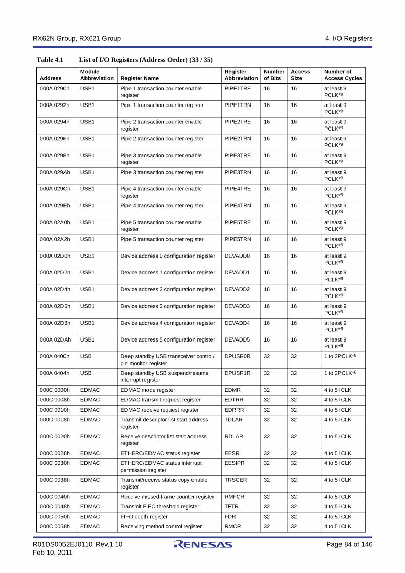
R01DS0052EJ0110 Rev.1.10 Page 84 of 146Feb 10, 2011
RX62N Group, RX621 Group 4. I/O Registers
000A 0290h USB1 Pipe 1 transaction counter enable register
PIPE1TRE 16 16 at least 9 PCLK*9
000A 0292h USB1 Pipe 1 transaction counter register PIPE1TRN 16 16 at least 9 PCLK*9
000A 0294h USB1 Pipe 2 transaction counter enable register
PIPE2TRE 16 16 at least 9 PCLK*9
000A 0296h USB1 Pipe 2 transaction counter register PIPE2TRN 16 16 at least 9 PCLK*9
000A 0298h USB1 Pipe 3 transaction counter enable register
PIPE3TRE 16 16 at least 9 PCLK*9
000A 029Ah USB1 Pipe 3 transaction counter register PIPE3TRN 16 16 at least 9 PCLK*9
000A 029Ch USB1 Pipe 4 transaction counter enable register
PIPE4TRE 16 16 at least 9 PCLK*9
000A 029Eh USB1 Pipe 4 transaction counter register PIPE4TRN 16 16 at least 9 PCLK*9
000A 02A0h USB1 Pipe 5 transaction counter enable register
PIPE5TRE 16 16 at least 9 PCLK*9
000A 02A2h USB1 Pipe 5 transaction counter register PIPE5TRN 16 16 at least 9 PCLK*9
000A 02D0h USB1 Device address 0 configuration register DEVADD0 16 16 at least 9 PCLK*9
000A 02D2h USB1 Device address 1 configuration register DEVADD1 16 16 at least 9 PCLK*9
000A 02D4h USB1 Device address 2 configuration register DEVADD2 16 16 at least 9 PCLK*9
000A 02D6h USB1 Device address 3 configuration register DEVADD3 16 16 at least 9 PCLK*9
000A 02D8h USB1 Device address 4 configuration register DEVADD4 16 16 at least 9 PCLK*9
000A 02DAh USB1 Device address 5 configuration register DEVADD5 16 16 at least 9 PCLK*9
000A 0400h USB Deep standby USB transceiver control/pin monitor register
DPUSR0R 32 32 1 to 2PCLK*8
000A 0404h USB Deep standby USB suspend/resume interrupt register
DPUSR1R 32 32 1 to 2PCLK*8
000C 0000h EDMAC EDMAC mode register EDMR 32 32 4 to 5 ICLK
000C 0008h EDMAC EDMAC transmit request register EDTRR 32 32 4 to 5 ICLK
000C 0010h EDMAC EDMAC receive request register EDRRR 32 32 4 to 5 ICLK
000C 0018h EDMAC Transmit descriptor list start address register
TDLAR 32 32 4 to 5 ICLK
000C 0020h EDMAC Receive descriptor list start address register
RDLAR 32 32 4 to 5 ICLK
000C 0028h EDMAC ETHERC/EDMAC status register EESR 32 32 4 to 5 ICLK
000C 0030h EDMAC ETHERC/EDMAC status interrupt permission register
EESIPR 32 32 4 to 5 ICLK
000C 0038h EDMAC Transmit/receive status copy enable register
TRSCER 32 32 4 to 5 ICLK
000C 0040h EDMAC Receive missed-frame counter register RMFCR 32 32 4 to 5 ICLK
000C 0048h EDMAC Transmit FIFO threshold register TFTR 32 32 4 to 5 ICLK
000C 0050h EDMAC FIFO depth register FDR 32 32 4 to 5 ICLK
000C 0058h EDMAC Receiving method control register RMCR 32 32 4 to 5 ICLK
Table 4.1 List of I/O Registers (Address Order) (33 / 35)
AddressModule Abbreviation Register Name
Register Abbreviation
Number of Bits
AccessSize
Number of Access Cycles

R01DS0052EJ0110 Rev.1.10 Page 85 of 146Feb 10, 2011
RX62N Group, RX621 Group 4. I/O Registers
000C 0064h EDMAC Transmit FIFO underrun counter TFUCR 32 32 4 to 5 ICLK
000C 0068h EDMAC Receive FIFO overflow counter RFOCR 32 32 4 to 5 ICLK
000C 006Ch EDMAC Independent output signal setting register
IOSR 32 32 4 to 5 ICLK
000C 0070h EDMAC Flow control start FIFO threshold setting register
FCFTR 32 32 4 to 5 ICLK
000C 0078h EDMAC Receive data padding insert register RPADIR 32 32 4 to 5 ICLK
000C 007Ch EDMAC Transmit interrupt setting register TRIMD 32 32 4 to 5 ICLK
000C 00C8h EDMAC Receive buffer write address register RBWAR 32 32 4 to 5 ICLK
000C 00CCh EDMAC Receive descriptor fetch address register RDFAR 32 32 4 to 5 ICLK
000C 00D4h EDMAC Transmit buffer read address register TBRAR 32 32 4 to 5 ICLK
000C 00D8h EDMAC Transmit descriptor fetch address register
TDFAR 32 32 4 to 5 ICLK
000C 0100h ETHERC ETHERC mode register ECMR 32 32 4 to 5 ICLK
000C 0108h ETHERC Receive frame length register RFLR 32 32 4 to 5 ICLK
000C 0110h ETHERC ETHERC status register ECSR 32 32 4 to 5 ICLK
000C 0118h ETHERC ETHERC interrupt enable register ECSIPR 32 32 4 to 5 ICLK
000C 0120h ETHERC PHY interface register PIR 32 32 4 to 5 ICLK
000C 0128h ETHERC PHY status register PSR 32 32 4 to 5 ICLK
000C 0140h ETHERC Random number generation counter upper limit setting register
RDMLR 32 32 4 to 5 ICLK
000C 0150h ETHERC IPG register IPGR 32 32 4 to 5 ICLK
000C 0154h ETHERC Automatic PAUSE frame register APR 32 32 4 to 5 ICLK
000C 0158h ETHERC Manual PAUSE frame register MPR 32 32 4 to 5 ICLK
000C 0160h ETHERC PAUSE frame receive counter register RFCF 32 32 4 to 5 ICLK
000C 0164h ETHERC Automatic PAUSE frame retransmit count register
TPAUSER 32 32 4 to 5 ICLK
000C 0168h ETHERC PAUSE frame retransmit counter register TPAUSECR 32 32 4 to 5 ICLK
000C 016Ch ETHERC Broadcast frame receive count setting register
BCFRR 32 32 4 to 5 ICLK
000C 01C0h ETHERC MAC address high register MAHR 32 32 4 to 5 ICLK
000C 01C8h ETHERC MAC address low register MALR 32 32 4 to 5 ICLK
000C 01D0h ETHERC Transmit retry over counter register TROCR 32 32 4 to 5 ICLK
000C 01D4h ETHERC Delayed collision detect counter register CDCR 32 32 4 to 5 ICLK
000C 01D8h ETHERC Lost carrier counter register LCCR 32 32 4 to 5 ICLK
000C 01DCh ETHERC Carrier not detect counter register CNDCR 32 32 4 to 5 ICLK
000C 01E4h ETHERC CRC error frame receive counter register CEFCR 32 32 4 to 5 ICLK
000C 01E8h ETHERC Frame receive error counter register FRECR 32 32 4 to 5 ICLK
000C 01ECh ETHERC Too-short frame receive counter register TSFRCR 32 32 4 to 5 ICLK
000C 01F0h ETHERC Too-long frame receive counter register TLFRCR 32 32 4 to 5 ICLK
000C 01F4h ETHERC Residual-bit frame receive counter register
RFCR 32 32 4 to 5 ICLK
000C 01F8h ETHERC Multicast address frame receive counter register
MAFCR 32 32 4 to 5 ICLK
007F C402h FLASH Flash mode register FMODR 8 8 2 to 3 PCLK*8
007F C410h FLASH Flash access status register FASTAT 8 8 2 to 3 PCLK*8
Table 4.1 List of I/O Registers (Address Order) (34 / 35)
AddressModule Abbreviation Register Name
Register Abbreviation
Number of Bits
AccessSize
Number of Access Cycles
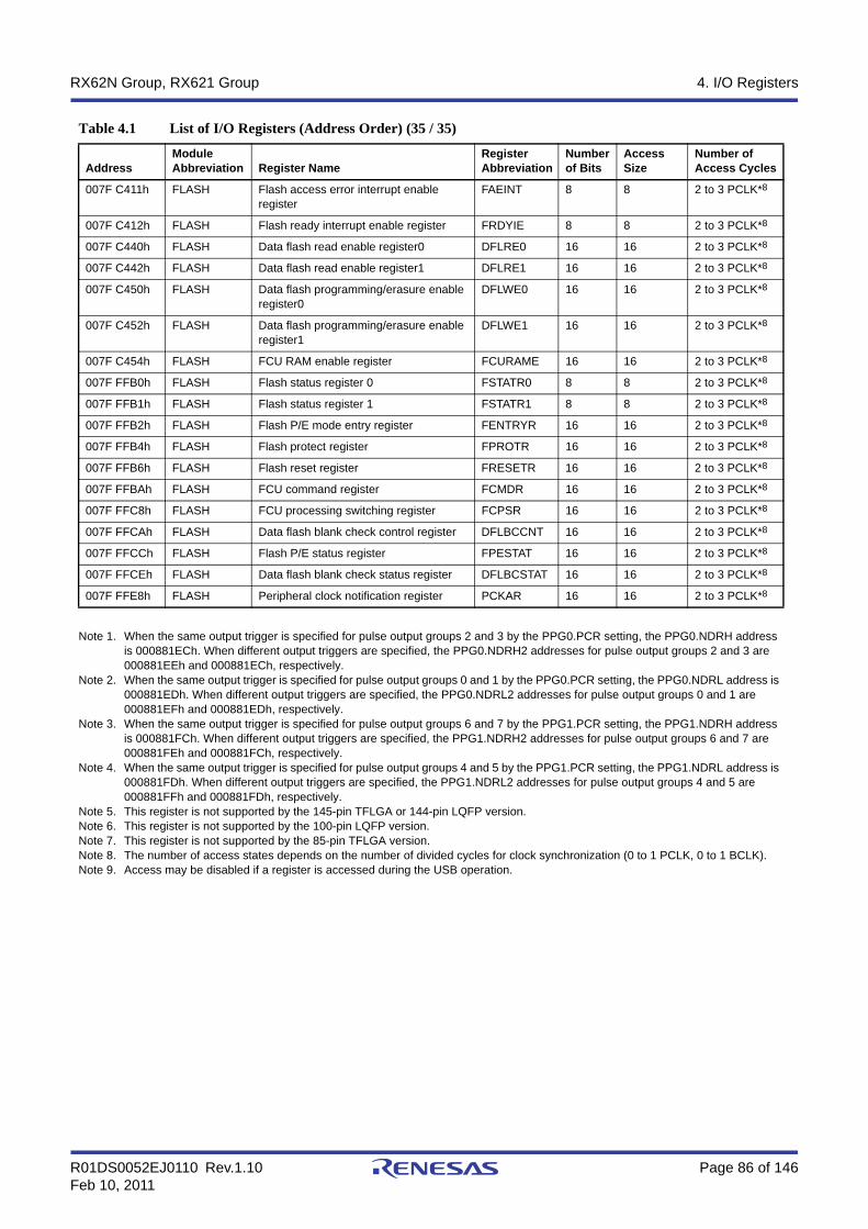
R01DS0052EJ0110 Rev.1.10 Page 86 of 146Feb 10, 2011
RX62N Group, RX621 Group 4. I/O Registers
Note 1. When the same output trigger is specified for pulse output groups 2 and 3 by the PPG0.PCR setting, the PPG0.NDRH address is 000881ECh. When different output triggers are specified, the PPG0.NDRH2 addresses for pulse output groups 2 and 3 are 000881EEh and 000881ECh, respectively.
Note 2. When the same output trigger is specified for pulse output groups 0 and 1 by the PPG0.PCR setting, the PPG0.NDRL address is 000881EDh. When different output triggers are specified, the PPG0.NDRL2 addresses for pulse output groups 0 and 1 are 000881EFh and 000881EDh, respectively.
Note 3. When the same output trigger is specified for pulse output groups 6 and 7 by the PPG1.PCR setting, the PPG1.NDRH address is 000881FCh. When different output triggers are specified, the PPG1.NDRH2 addresses for pulse output groups 6 and 7 are 000881FEh and 000881FCh, respectively.
Note 4. When the same output trigger is specified for pulse output groups 4 and 5 by the PPG1.PCR setting, the PPG1.NDRL address is 000881FDh. When different output triggers are specified, the PPG1.NDRL2 addresses for pulse output groups 4 and 5 are 000881FFh and 000881FDh, respectively.
Note 5. This register is not supported by the 145-pin TFLGA or 144-pin LQFP version.Note 6. This register is not supported by the 100-pin LQFP version.Note 7. This register is not supported by the 85-pin TFLGA version.Note 8. The number of access states depends on the number of divided cycles for clock synchronization (0 to 1 PCLK, 0 to 1 BCLK).Note 9. Access may be disabled if a register is accessed during the USB operation.
007F C411h FLASH Flash access error interrupt enable register
FAEINT 8 8 2 to 3 PCLK*8
007F C412h FLASH Flash ready interrupt enable register FRDYIE 8 8 2 to 3 PCLK*8
007F C440h FLASH Data flash read enable register0 DFLRE0 16 16 2 to 3 PCLK*8
007F C442h FLASH Data flash read enable register1 DFLRE1 16 16 2 to 3 PCLK*8
007F C450h FLASH Data flash programming/erasure enable register0
DFLWE0 16 16 2 to 3 PCLK*8
007F C452h FLASH Data flash programming/erasure enable register1
DFLWE1 16 16 2 to 3 PCLK*8
007F C454h FLASH FCU RAM enable register FCURAME 16 16 2 to 3 PCLK*8
007F FFB0h FLASH Flash status register 0 FSTATR0 8 8 2 to 3 PCLK*8
007F FFB1h FLASH Flash status register 1 FSTATR1 8 8 2 to 3 PCLK*8
007F FFB2h FLASH Flash P/E mode entry register FENTRYR 16 16 2 to 3 PCLK*8
007F FFB4h FLASH Flash protect register FPROTR 16 16 2 to 3 PCLK*8
007F FFB6h FLASH Flash reset register FRESETR 16 16 2 to 3 PCLK*8
007F FFBAh FLASH FCU command register FCMDR 16 16 2 to 3 PCLK*8
007F FFC8h FLASH FCU processing switching register FCPSR 16 16 2 to 3 PCLK*8
007F FFCAh FLASH Data flash blank check control register DFLBCCNT 16 16 2 to 3 PCLK*8
007F FFCCh FLASH Flash P/E status register FPESTAT 16 16 2 to 3 PCLK*8
007F FFCEh FLASH Data flash blank check status register DFLBCSTAT 16 16 2 to 3 PCLK*8
007F FFE8h FLASH Peripheral clock notification register PCKAR 16 16 2 to 3 PCLK*8
Table 4.1 List of I/O Registers (Address Order) (35 / 35)
AddressModule Abbreviation Register Name
Register Abbreviation
Number of Bits
AccessSize
Number of Access Cycles
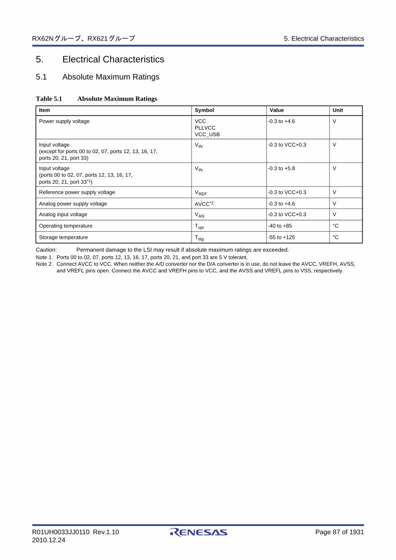
R01UH0033JJ0110 Rev.1.10 Page 87 of 19312010.12.24
RX62Nグループ、RX621グループ 5. Electrical Characteristics
5. Electrical Characteristics
5.1 Absolute Maximum Ratings
Caution: Permanent damage to the LSI may result if absolute maximum ratings are exceeded.Note 1. Ports 00 to 02, 07, ports 12, 13, 16, 17, ports 20, 21, and port 33 are 5 V tolerant.Note 2. Connect AVCC to VCC. When neither the A/D converter nor the D/A converter is in use, do not leave the AVCC, VREFH, AVSS,
and VREFL pins open. Connect the AVCC and VREFH pins to VCC, and the AVSS and VREFL pins to VSS, respectively.
Table 5.1 Absolute Maximum Ratings
Item Symbol Value Unit
Power supply voltage VCCPLLVCC VCC_USB
-0.3 to +4.6 V
Input voltage(except for ports 00 to 02, 07, ports 12, 13, 16, 17, ports 20, 21, port 33)
VIN -0.3 to VCC+0.3 V
Input voltage(ports 00 to 02, 07, ports 12, 13, 16, 17, ports 20, 21, port 33*1)
VIN -0.3 to +5.8 V
Reference power supply voltage VREF -0.3 to VCC+0.3 V
Analog power supply voltage AVCC*2 -0.3 to +4.6 V
Analog input voltage VAN -0.3 to VCC+0.3 V
Operating temperature Topr -40 to +85 °C
Storage temperature Tstg -55 to +125 °C

R01UH0033JJ0110 Rev.1.10 Page 88 of 19312010.12.24
RX62Nグループ、RX621グループ 5. Electrical Characteristics
5.2 DC Characteristics
Table 5.2 DC Characteristics (1)Conditions: VCC = PLLVCC = AVCC = VCC_USB = 2.7 to 3.6V, VREFH = 2.7V to AVCC
VSS = PLLVSS = AVSS = VREFL = VSS_USB = 0V
Ta = -40 to +85C
Item Symbol Min. Typ. Max. Unit Test Conditions
Schmitt trigger input voltage*2
IRQ input pin*1
MTU input pin*1
TMR input pin*1
SCI input pin*1
ADTRG input pin*1
RES#, NMI
VIH VCC × 0.8 — VCC+0.3 V
VIL -0.3 — VCC × 0.2
ΔVT VCC × 0.06 — —
RIIC input pin(except for SMBus)
VIH VCC × 0.7 — 5.8
VIL -0.3 — VCC × 0.3
ΔVT VCC × 0.05 — —
Ports 00 to 02, 07ports 12, 13, 16, 17ports 20, 21port 33
VIH VCC × 0.8 — 5.8
VIL -0.3 — VCC × 0.2
Ports 03, 05, 10, 11, 14, 15ports 22 to 27ports 30 to 32, 34, 35ports 4 to GOther input pins
VIH VCC × 0.8 — VCC+0.3
VIL -0.3 — VCC × 0.2
Input high voltage (except Schmitt trigger input pin)
MD pin, EMLE VIH VCC × 0.9 — VCC+0.3 V
EXTAL, RSPI, ETHERCEXDMAC, WAIT#, TCK
VCC × 0.8 — VCC+0.3
XCIN VCC × 0.8 — VCC+0.3
D0 to D31 VCC × 0.7 — VCC+0.3
RIIC (SMBus) 2.1 — VCC+0.3
Input low voltage (except Schmitt trigger input pin)
MD pin, EMLE VIL -0.3 — VCC × 0.1 V
EXTAL, RSPI, ETHERCEXDMAC, WAIT#, TCK
-0.3 — VCC × 0.2
XCIN -0.3 — VCC×0.2
D0 to D31 -0.3 — VCC×0.3
RIIC (SMBus) -0.3 — 0.8

R01UH0033JJ0110 Rev.1.10 Page 89 of 19312010.12.24
RX62Nグループ、RX621グループ 5. Electrical Characteristics
Table 5.3 DC Characteristics (2)Conditions: VCC = PLLVCC = AVCC = VCC_USB = 2.7 to 3.6V, VREFH = 2.7V to AVCC
VSS = PLLVSS = AVSS = VREFL = VSS_USB = 0V
Ta = -40 to +85C
Item Symbol Min. Typ. Max. Unit Test Conditions
Output high voltage
All output pins VOH VCC-0.5 — — V IOH = -1mA
Output low voltage
All output pins(except for RIIC pins)
VOL — — 0.5 V IOL = 1.0mA
RIIC pins — — 0.4 V IOL = 3.0mA
— — 0.6 IOL = 6.0mA
RIIC pins(only P12 and P13 in channel 0)
VOL — — 0.4 V IOL = 15.0mA
(ICFER.FMPE = 1)
— 0.4 — IOL = 20.0mA
(ICFER.FMPE = 1)
Input leakage current
RES#, MD pin, EMLE, NMI | Iin | — — 1.0 µA Vin = 0V
Vin = VCC
Three-state leakage current (off state)
Ports 03, 05, 10, 11, 14, 15ports 22 to 27ports 30 to 32, 34, 35ports 4 to G
| ITSI | — — 1.0 µA Vin = 0V
Vin = VCC
Ports 00 to 02, 07, 12, 13Ports 16, 17, 20, 21, 33
— — 5.0
Input pull-up MOS current
Ports 9 to E, G -Ip 10 — 300 µA VCC = 2.7 to 3.6VVin = 0V
Input capacitance
All input pins(except for ports 12, 13, 20, 21ports 40 to 47, and EMLE)
Cin — — 15 pF Vin = 0V
f = 1MHzTa = 25°C
Ports 12, 13, 20, 21, Ports 40 to 47, EMLE
— — 30

R01UH0033JJ0110 Rev.1.10 Page 90 of 19312010.12.24
RX62Nグループ、RX621グループ 5. Electrical Characteristics
Note 1. This does not include the pins, which are multiplexed as ports 00 to 02, 07, ports 12, 13, 16, 17, ports 20, 21, and port 33 for 5 V tolerant.
Note 2. Supply current values are with all output pins unloaded and all input pull-up MOSs in the off state.Note 3. Measured with clocks supplied to the peripheral functions. This does not include the BGO operation.Note 4. ICC depends on f (ICLK) as follows. (ICLK: PCLK: BCLK = 8 : 4: 2)
ICC max. = 0.89 x f + 11 (max.)ICC typ. = 0.43 x f + 5 (normal operation, peripheral function: clocks supplied)ICC typ. = 0.30 x f + 5 (normal operation, peripheral function: clocks not supplied)ICC max. = 0.48 x f + 12 (sleep mode)
Note 5. This does not include the BGO operation.Note 6. Incremented if data is written to or erased from the ROM or data flash for data storage during the program execution.Note 7. The values are for reference.
Table 5.4 DC Characteristics (3)Conditions: VCC = PLLVCC = AVCC = VCC_USB = 2.7 to 3.6V, VREFH = 2.7V to AVCC
VSS = PLLVSS = AVSS = VREFL = VSS_USB = 0V
Ta = -40 to +85C
Item Symbol Min. Typ. Max. Unit Test Conditions
Supply current*2
In operation Max.*3 ICC*4 — — 100 mA ICLK = 100MHz
PCLK = 50MHzBCLK = 50MHz
Peripheral function: Clocks supplied*5
— 48 —
Peripheral function Clocks not supplied*5
— 15 —
Sleep — 20 60
All-module-clock-stop mode*7 — 14 28
Standby mode
Software standby mode — 0.12 3.0 mA
Deep software standby mode
RTCin operation
RAM, USB retained
— 30 206 µA
RAM, USB power supply halted
— 26 66 µA
RTChalted
RAM, USB retained
— 25 200 µA
RAM, USB power supply halted
— 21 60 µA
Analog power supply current
During 12-bit A/D conversion (per unit) AICC — 2.5 3.0 mA
During 10-bit A/D conversion (per unit) — 0.8 1.2 mA
During D/A conversion (per unit) — 0.3 2.0 µA
Idle (all units) — 30 35 µA
Reference power supply current
During 12-bit A/D conversion (per unit) AICC — 0.5 0.7 mA
During 10-bit A/D conversion (per unit) — 0.06 0.1 mA
During D/A conversion (per unit) — 0.6 1.0 mA
Idle (all units) — 0.4 0.6 mA
RAM standby voltage VRAM 2.48 — — V
VCC rising gradient SVCC — — 20 ms/V
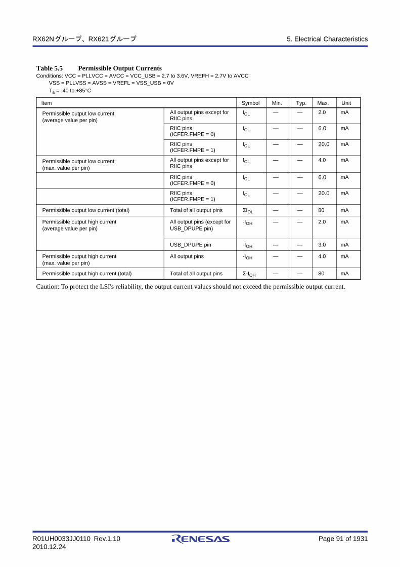
R01UH0033JJ0110 Rev.1.10 Page 91 of 19312010.12.24
RX62Nグループ、RX621グループ 5. Electrical Characteristics
Caution: To protect the LSI's reliability, the output current values should not exceed the permissible output current.
Table 5.5 Permissible Output CurrentsConditions: VCC = PLLVCC = AVCC = VCC_USB = 2.7 to 3.6V, VREFH = 2.7V to AVCC
VSS = PLLVSS = AVSS = VREFL = VSS_USB = 0V
Ta = -40 to +85C
Item Symbol Min. Typ. Max. Unit
Permissible output low current (average value per pin)
All output pins except for RIIC pins
IOL — — 2.0 mA
RIIC pins(ICFER.FMPE = 0)
IOL — — 6.0 mA
RIIC pins(ICFER.FMPE = 1)
IOL — — 20.0 mA
Permissible output low current (max. value per pin)
All output pins except for RIIC pins
IOL — — 4.0 mA
RIIC pins(ICFER.FMPE = 0)
IOL — — 6.0 mA
RIIC pins(ICFER.FMPE = 1)
IOL — — 20.0 mA
Permissible output low current (total) Total of all output pins ΣIOL — — 80 mA
Permissible output high current (average value per pin)
All output pins (except for USB_DPUPE pin)
-IOH — — 2.0 mA
USB_DPUPE pin -IOH — — 3.0 mA
Permissible output high current (max. value per pin)
All output pins -IOH — — 4.0 mA
Permissible output high current (total) Total of all output pins Σ-IOH — — 80 mA
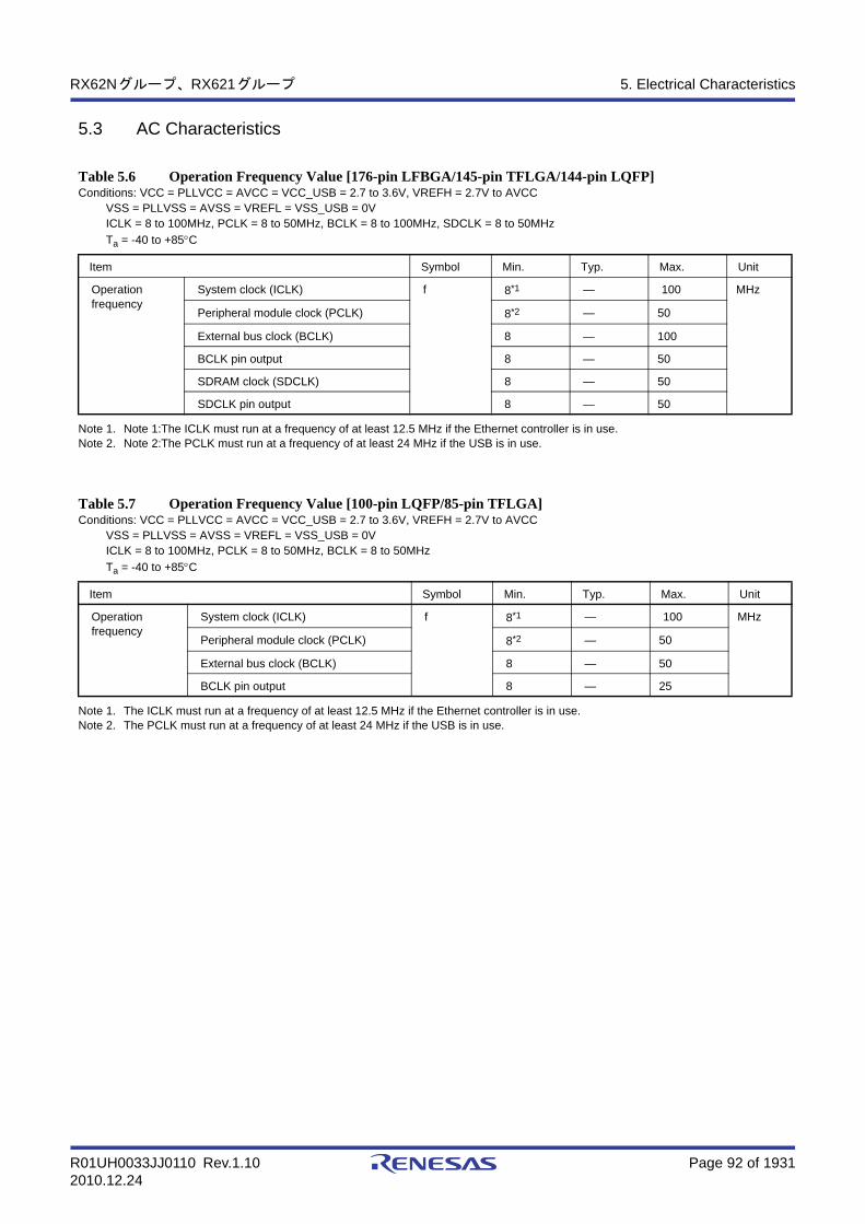
R01UH0033JJ0110 Rev.1.10 Page 92 of 19312010.12.24
RX62Nグループ、RX621グループ 5. Electrical Characteristics
5.3 AC Characteristics
Note 1. Note 1:The ICLK must run at a frequency of at least 12.5 MHz if the Ethernet controller is in use.Note 2. Note 2:The PCLK must run at a frequency of at least 24 MHz if the USB is in use.
Note 1. The ICLK must run at a frequency of at least 12.5 MHz if the Ethernet controller is in use.Note 2. The PCLK must run at a frequency of at least 24 MHz if the USB is in use.
Table 5.6 Operation Frequency Value [176-pin LFBGA/145-pin TFLGA/144-pin LQFP]Conditions: VCC = PLLVCC = AVCC = VCC_USB = 2.7 to 3.6V, VREFH = 2.7V to AVCC
VSS = PLLVSS = AVSS = VREFL = VSS_USB = 0VICLK = 8 to 100MHz, PCLK = 8 to 50MHz, BCLK = 8 to 100MHz, SDCLK = 8 to 50MHz
Ta = -40 to +85C
Item Symbol Min. Typ. Max. Unit
Operationfrequency
System clock (ICLK) f 8*1 — 100 MHz
Peripheral module clock (PCLK) 8*2 — 50
External bus clock (BCLK) 8 — 100
BCLK pin output 8 — 50
SDRAM clock (SDCLK) 8 — 50
SDCLK pin output 8 — 50
Table 5.7 Operation Frequency Value [100-pin LQFP/85-pin TFLGA]Conditions: VCC = PLLVCC = AVCC = VCC_USB = 2.7 to 3.6V, VREFH = 2.7V to AVCC
VSS = PLLVSS = AVSS = VREFL = VSS_USB = 0VICLK = 8 to 100MHz, PCLK = 8 to 50MHz, BCLK = 8 to 50MHz
Ta = -40 to +85C
Item Symbol Min. Typ. Max. Unit
Operationfrequency
System clock (ICLK) f 8*1 — 100 MHz
Peripheral module clock (PCLK) 8*2 — 50
External bus clock (BCLK) 8 — 50
BCLK pin output 8 — 25

R01UH0033JJ0110 Rev.1.10 Page 93 of 19312010.12.24
RX62Nグループ、RX621グループ 5. Electrical Characteristics
5.3.1 Clock Timing
Table 5.8 Clock TimingConditions: VCC = PLLVCC = AVCC = VCC_USB = 2.7 to 3.6V, VREFH = 2.7V to AVCC
VSS = PLLVSS = AVSS = VREFL = VSS_USB = 0V
Ta = -40 to +85C
Item Symbol Min. Max. Unit Test Conditions
BCLK pin output cycle time[176-pin LFBGA/145-pin TFLGA/144-pin LQFP]
tBcyc 20 125 ns Figure 5.1
BCLK pin output cycle time[100-pin LQFP/85-pin TFLGA]
tBcyc 40 125 ns
BCLK pin output high pulse width tCH 5 — ns
BCLK pin output low pulse width tCL 5 — ns
BCLK pin output rising time tCr — 5 ns
BCLK pin output falling time tCf — 5 ns
SDCLK pin output cycle time tSDcyc 20 125 ns
SDCLK pin output high pulse width tCH 5 — ns
SDCLK pin output low pulse width tCL 5 — ns
SDCLK pin output rising time tCr — 5 ns
SDCLK pin output falling time tCf — 5 ns
Oscillation settling time after reset (crystal) tOSC1 10 — ms Figure 5.2
Oscillation settling time after leaving software standby mode (crystal)
tOSC2 10 — ms Figure 5.3
Oscillation settling time after leaving deep software standby mode (crystal)
tOSC3 10 — ms Figure 5.4
EXTAL external clock output delay settling time tDEXT 1 — ms Figure 5.2
EXTAL external clock input low pulse width tEXL 35.71 — ns Figure 5.5
EXTAL external clock input high pulse width tEXH 35.71 — ns
EXTAL external clock rising time tEXr — 5 ns
EXTAL external clock falling time tEXf — 5 ns
XCIN sub-clock oscillation settling time tSUBOSC 2 — s Figure 5.6
XCIN sub-clock oscillation frequency fSUB 32.768 — kHz
On-chip oscillator (IWDTCLK) oscillation frequency fIWDTCLK 62.5 187.5 kHz

R01UH0033JJ0110 Rev.1.10 Page 94 of 19312010.12.24
RX62Nグループ、RX621グループ 5. Electrical Characteristics
Figure 5.1 BCLK Pin Output, SDCLK Pin Output Timing
Figure 5.2 Oscillation Settling Timing
Figure 5.3 Oscillation Settling Timing after Software Standby Mode
tCH
tBcyc, tSDcyc
tCf
tCL
tCr
Test conditions: VOH = VCC x 0.7, VOL = VCC x 0.3, IOH = -1.0mA, IOL = 1.0mA, C = 30pF
BCLK pin output, SDCLK pin output
tOSC1
tDEXT
VCC
EXTAL
RES#
ICLK
Software standby mode (power-down mode)
IRQ exception handlingIRQMD[1:0] = 10bSSBY = 1
WAIT instructionOscillation
settling timetOSC2
IRQ exception handling
01 10
SSBY
IRQCRn.IRQMD[1:0]
IRQ
ICLK
Oscillator

R01UH0033JJ0110 Rev.1.10 Page 95 of 19312010.12.24
RX62Nグループ、RX621グループ 5. Electrical Characteristics
Figure 5.4 Oscillation Settling Timing after Deep Software Standby Mode
Invalid by the internal reset
IRQ exception handlingDIRQnEG = 1SSBY = 1
Deep software standby mode
(power-down mode)Reset exception handling
Oscillation settling time
tOSC3
WAIT instruction
When IOKEEP=L
Operating
When IOKEEP=H
Oscillator
ICLK
IRQ
IRQ interrupt
DIRQnF set request Set
DIRQnEG bit Set
DPSBY bit Set
IOKEEP bit ClearedSetL
I/O port Operating Retained
IOKEEP bit
I/O port Operating Retained Operating
DPSRSTF flag
Internal reset
L
H

R01UH0033JJ0110 Rev.1.10 Page 96 of 19312010.12.24
RX62Nグループ、RX621グループ 5. Electrical Characteristics
Figure 5.5 EXTAL External Input Clock Timing
Figure 5.6 XCIN Sub-Clock Oscillation Settling Time
tEXf
VCC×0.5EXTAL
tEXH tEXL
tEXr
XCIN
VCC tSUBOSC
Oscillation settling time
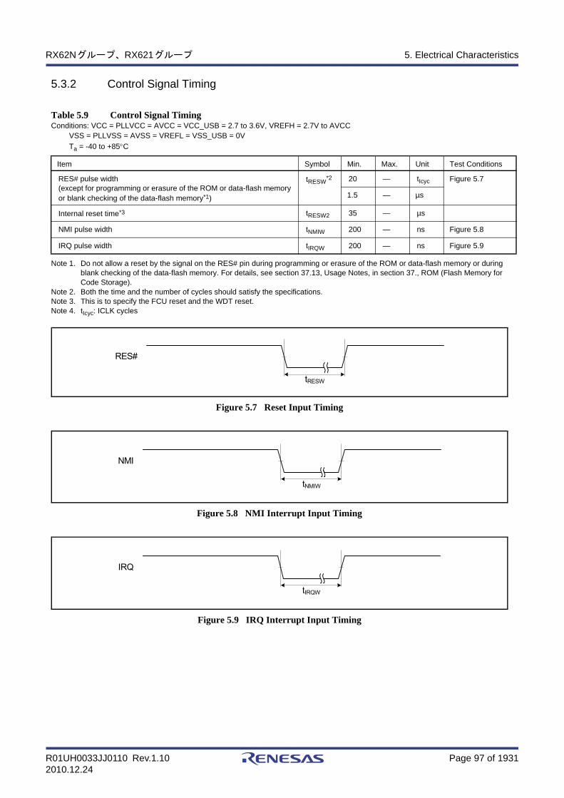
R01UH0033JJ0110 Rev.1.10 Page 97 of 19312010.12.24
RX62Nグループ、RX621グループ 5. Electrical Characteristics
5.3.2 Control Signal Timing
Note 1. Do not allow a reset by the signal on the RES# pin during programming or erasure of the ROM or data-flash memory or during blank checking of the data-flash memory. For details, see section 37.13, Usage Notes, in section 37., ROM (Flash Memory for Code Storage).
Note 2. Both the time and the number of cycles should satisfy the specifications.Note 3. This is to specify the FCU reset and the WDT reset.Note 4. tIcyc: ICLK cycles
Figure 5.7 Reset Input Timing
Figure 5.8 NMI Interrupt Input Timing
Figure 5.9 IRQ Interrupt Input Timing
Table 5.9 Control Signal TimingConditions: VCC = PLLVCC = AVCC = VCC_USB = 2.7 to 3.6V, VREFH = 2.7V to AVCC
VSS = PLLVSS = AVSS = VREFL = VSS_USB = 0V
Ta = -40 to +85C
Item Symbol Min. Max. Unit Test Conditions
RES# pulse width (except for programming or erasure of the ROM or data-flash memory or blank checking of the data-flash memory*1)
tRESW*2 20 — tIcyc Figure 5.7
1.5 — µs
Internal reset time*3 tRESW2 35 — µs
NMI pulse width tNMIW 200 — ns Figure 5.8
IRQ pulse width tIRQW 200 — ns Figure 5.9
RES#
tRESW
NMI
tNMIW
IRQ
tIRQW

R01UH0033JJ0110 Rev.1.10 Page 98 of 19312010.12.24
RX62Nグループ、RX621グループ 5. Electrical Characteristics
5.3.3 Bus Timing
Table 5.10 Bus Timing [176-pin LFBGA/145-pin TFLGA/144-pin LQFP]Conditions: VCC = PLLVCC = AVCC = VCC_USB = 2.7 to 3.6V, VREFH = 2.7V to AVCC
VSS = PLLVSS = AVSS = VREFL = VSS_USB = 0VICLK = 8 to 100MHz, BCLK = 8 to 100MHz, SDCLK = 8 to 50MHz
Ta = -40 to +85C
Output load conditions: VOH = VCC×0.5, VOL = VCC×0.5, IOH = -1.0mA, IOL = 1.0mA, C = 30pF
Item Symbol Min. Max. Unit Test Conditions
Address delay time tAD— 15 ns Figure 5.10 to Figure 5.13
Byte control delay time tBCD— 15 ns
CS# delay time tCSD— 15 ns
RD# delay time tRSD— 15 ns
Read data setup time tRDS15 — ns
Read data hold time tRDH0.0 — ns
WR# delay time tWRD— 15 ns
Write data delay time tWDD— 15 ns
Write data hold time tWDH0 — ns
WAIT# setup time tWTS15 — ns Figure 5.14
WAIT# hold time tWTH0.0 — ns
Address delay time 2 (SDRAM) tAD21 15 ns Figure 5.22 to Figure 5.28
CS# delay time 2 (SDRAM) tCSD21 15 ns
DQM delay time (SDRAM) tDQMD1 15 ns
CKE delay time (SDRAM) tCKED1 15 ns
Read data setup time 2 (SDRAM) tRDS212 — ns
Read data hold time 2 (SDRAM) tRDH20 — ns
Write data delay time 2 (SDRAM) tWDD2— 15 ns
Write data hold time 2 (SDRAM) tWDH21 — ns
WE# delay time (SDRAM) tWED1 15 ns
RAS# delay time (SDRAM) tRASD1 15 ns
CAS# delay time (SDRAM) tCASD1 15 ns
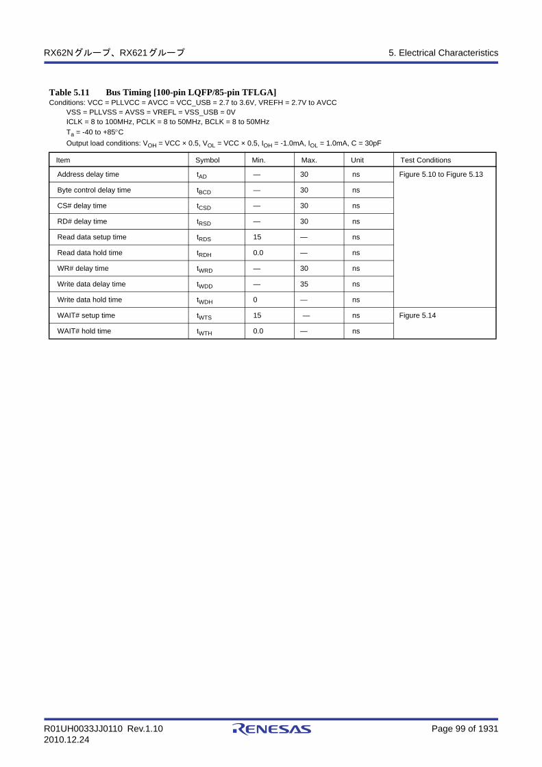
R01UH0033JJ0110 Rev.1.10 Page 99 of 19312010.12.24
RX62Nグループ、RX621グループ 5. Electrical Characteristics
Table 5.11 Bus Timing [100-pin LQFP/85-pin TFLGA]Conditions: VCC = PLLVCC = AVCC = VCC_USB = 2.7 to 3.6V, VREFH = 2.7V to AVCC
VSS = PLLVSS = AVSS = VREFL = VSS_USB = 0VICLK = 8 to 100MHz, PCLK = 8 to 50MHz, BCLK = 8 to 50MHz
Ta = -40 to +85COutput load conditions: VOH = VCC × 0.5, VOL = VCC × 0.5, IOH = -1.0mA, IOL = 1.0mA, C = 30pF
Item Symbol Min. Max. Unit Test Conditions
Address delay time tAD — 30 ns Figure 5.10 to Figure 5.13
Byte control delay time tBCD — 30 ns
CS# delay time tCSD — 30 ns
RD# delay time tRSD — 30 ns
Read data setup time tRDS 15 — ns
Read data hold time tRDH 0.0 — ns
WR# delay time tWRD — 30 ns
Write data delay time tWDD — 35 ns
Write data hold time tWDH 0 — ns
WAIT# setup time tWTS 15 — ns Figure 5.14
WAIT# hold time tWTH 0.0 — ns
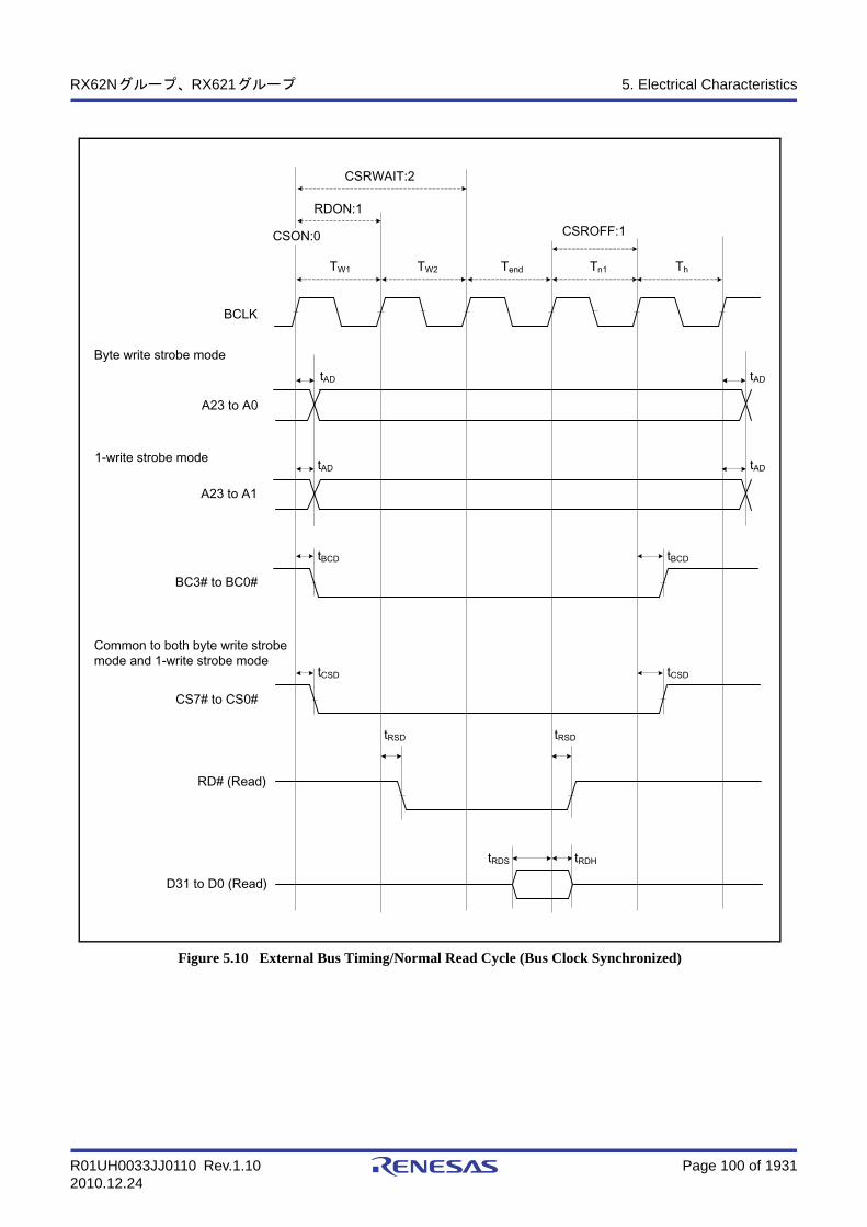
R01UH0033JJ0110 Rev.1.10 Page 100 of 19312010.12.24
RX62Nグループ、RX621グループ 5. Electrical Characteristics
Figure 5.10 External Bus Timing/Normal Read Cycle (Bus Clock Synchronized)
A23 to A1
CS7# to CS0#
tAD
BCLK
A23 to A0
D31 to D0 (Read)
Byte write strobe mode
1-write strobe mode
BC3# to BC0#
Common to both byte write strobe mode and 1-write strobe mode
tBCD
tCSD tCSD
RD# (Read)
tRSD tRSD
tAD
tRDHtRDS
tAD
tAD
tBCD
TW1 TW2 Tend Tn1 Th
RDON:1
CSRWAIT:2
CSROFF:1CSON:0

R01UH0033JJ0110 Rev.1.10 Page 101 of 19312010.12.24
RX62Nグループ、RX621グループ 5. Electrical Characteristics
Figure 5.11 External Bus Timing/Normal Write Cycle (Bus Clock Synchronized)
A23 to A1
CS7# to CS0#
tAD
BCLK
A23 to A0
Byte write strobe mode
1-write strobe mode
BC3# to BC0#
Common to both byte write strobe mode and 1-write strobe mode
tBCD
tCSD tCSD
tAD
tAD
tAD
tBCD
D31 to D0 (Write)
WR3# to WR0#, WR# (Write)
tWRD tWRD
tWDH
tWDD
TW1 TW2 Tend Tn1 Th
WRON:1WDON:1*1
CSWWAIT:2
CSWOFF:1WDOFF:1*1CSON:0
Note1: Be sure to specify WDON and WDOFF as at least one cycle of BCLK.

R01UH0033JJ0110 Rev.1.10 Page 102 of 19312010.12.24
RX62Nグループ、RX621グループ 5. Electrical Characteristics
Figure 5.12 External Bus Timing/Page Read Cycle (Bus Clock Synchronized)
Figure 5.13 External Bus Timing/Page Write Cycle (Bus Clock Synchronized)
A23 to A1
CS7# to CS0#
tAD
BCLK
A23 to A0
D31 to D0 (Read)
Byte write strobe mode
1-write strobe mode
BC3# to BC0#
Common to both byte write strobe mode and 1-write strobe mode
tBCD
tCSD tCSD
RD# (Read)
tRSD tRSD
tRDHtRDS
tAD
tBCD
TW1 TW2 Tend Tpw1 Tpw2
tAD tAD
tRSD tRSD
tRDHtRDS
tRSD tRSD
tRDHtRDS
Tend Tpw1 Tpw2 Tend Tn1 Th
tAD tAD tAD tAD
RDON:1
CSRWAIT:2
CSROFF:1
tRSD tRSD
tRDHtRDS
tAD
tAD
CSPRWAIT:2
Tpw1 Tpw2 Tend
RDON:1
CSPRWAIT:2
RDON:1
CSPRWAIT:2
RDON:1
CSON:0
A23 to A1
CS7# to CS0#
tAD
BCLK
A23 to A0
Byte write strobe mode
1-write strobe mode
BC3# to BC0#
Common to both byte write strobe mode and 1-write strobe mode
tBCD
tCSD tCSD
tAD
tBCD
TW1
D31 to D0 (Write)
WR3# to WR0#, WR# (Write)
tWRD tWRD
tWDHtWDD
TW2 Tend Tpw1 Tpw2
tAD tAD
tWRD tWRD
tWDHtWDD
tWRD tWRD
tWDHtWDD
Tdw1 Tend Tpw1 Tpw2 Tend Tn1 ThTdw1
tAD tAD tAD tAD
WRON:1WDON:1*1
CSWWAIT:2 CSPWWAIT:2
WDOFF:1*1
CSPWWAIT:2
WDOFF:1*1CSWOFF:1WDOFF:1*1
CSON:0
Note1: Be sure to specify WDON and WDOFF as at least one cycle of BCLK.
WRON:1WDON:1*1
WRON:1WDON:1*1

R01UH0033JJ0110 Rev.1.10 Page 103 of 19312010.12.24
RX62Nグループ、RX621グループ 5. Electrical Characteristics
Figure 5.14 External Bus Timing/External Wait Control
tWTS tWTH tWTS tWTH
CSRWAIT:3CSWWAIT:3
BCLK
A23 to A0
CS7# to CS0#
RD# (Read)
WR# (Write)
WAIT#
TW1 TW2 (Tend) TendTW3 Tn1 Th
External wait

R01UH0033JJ0110 Rev.1.10 Page 104 of 19312010.12.24
RX62Nグループ、RX621グループ 5. Electrical Characteristics
Figure 5.15 SDRAM Space Single Read Bus Timing
tAD2
SDCLK
A18 to A0
SDCS#
AP*1
DQMn
D31 to D0
RAS#
CAS#
WE#
CKE
Note 1: Address pins for output of the precharge-setting command (Precharge-sel) for SDRAM.
tDQMD
(High)
RowAddress Column Address
SDRAM command ACT RD PRA
tAD2
tCSD2
tRASD
tAD2
tAD2
tCSD2
tRASD
tAD2
tAD2
tCSD2
tRASD
tAD2
tAD2
tCSD2
tRASD
tWED tWED
tCSD2 tCSD2
tCASD tCASD
tRDS2 tRDH2
PRA Command

R01UH0033JJ0110 Rev.1.10 Page 105 of 19312010.12.24
RX62Nグループ、RX621グループ 5. Electrical Characteristics
Figure 5.16 SDRAM Space Single Write Bus Timing
tAD2
SDCLK
A18 to A0
SDCS#
AP*1
DQMn
D31 to D0
RAS#
CAS#
WE#
CKE
Note 1: Address pins for output of the precharge-setting command (Precharge-sel) for SDRAM.
tDQMD
(High)
RowAddress Column Address
SDRAM command ACT WR PRA
tAD2
tCSD2
tRASD
tWED
tCASD
tWDD2
tAD2
tAD2
tCSD2
tRASD
tAD2
tAD2
tCSD2
tRASD
tAD2
tAD2
tCSD2
tRASD
tCSD2 tCSD2
tCASD
tWED tWED tWED
tWDH2
PRA command

R01UH0033JJ0110 Rev.1.10 Page 106 of 19312010.12.24
RX62Nグループ、RX621グループ 5. Electrical Characteristics
Figure 5.17 SDRAM Space Multiple Read Bus Timing
SDCLK
Note 1: Address pins for output of the precharge-setting command (Precharge-sel) for SDRAM.
ACT RD RD RD RD PRA
A18 to A0
tAD2 tAD2 tAD2 tAD2 tAD2 tAD2 tAD2 tAD2
AP*1
SDCS#
RAS#
CAS#
WE#
CKE
DQMn
D31 to D0
C1 C2 C3RowAddress
C0 (Column Address)
tAD2 tAD2 tAD2 tAD2 tAD2
tCSD2 tCSD2 tCSD2 tCSD2 tCSD2
tRAS
D
tRAS
D
tRAS
D
tRAS
D
tRAS
D
tCAS
D
tCAS
DtCAS
D
tWED tWED
(High)
tDQMD tDQMD
tRDS2 tRDH2 tRDS2 tRDH2
PRAcommand

R01UH0033JJ0110 Rev.1.10 Page 107 of 19312010.12.24
RX62Nグループ、RX621グループ 5. Electrical Characteristics
Figure 5.18 SDRAM Space Multiple Write Bus Timing
ACT WR PRAWR WR WR
SDCLK
A18 to A0
AP*1
SDCS#
RAS#
CAS#
WE#
CKE
DQMn
D31 to D0
tAD2 tAD2 tAD2 tAD2 tAD2 tAD2 tAD2 tAD2
tAD2 tAD2 tAD2 tAD2 tAD2
tCSD2 tCSD2 tCSD2 tCSD2 tCSD2
tRAS
D
tRAS
D
tRAS
D
tRAS
D
tRAS
D
tCAS
DtCAS
D
tCAS
D
tWED tWED
(High)
tDQMD tDQMD
tWDD2 tWDH2 tWDD2 tWDH2
C1 C2 C3RowAddress
C0 (Column Address)
PRAcommand
Note 1: Address pins for output of the precharge-setting command (Precharge-sel) for SDRAM.

R01UH0033JJ0110 Rev.1.10 Page 108 of 19312010.12.24
RX62Nグループ、RX621グループ 5. Electrical Characteristics
Figure 5.19 SDRAM Space Multiple Read Line Stride Bus Timing
R1A18 to A0
SDCLK
SDCS#
AP*1
DQMn
D31 to D0
RAS#
CAS#
WE#
CKE
SDRAM command
Note 1: Address pins for output of the precharge-setting command (Precharge-sel) for SDRAM.
ACT RD RD RD RD PRA ACT RD RD RD RD PRA
tCASD
tRASD
tCSD2
t AD2 t AD2 t AD2 t AD2 t AD2 t AD2 t AD2 t AD2 t AD2 t AD2 t AD2 t AD2 t AD2 t AD2
t AD2 t AD2 t AD2 t AD2 t AD2 t AD2 t AD2 t AD2
tCSD2 tCSD2 t CSD2 tCSD2 tCSD2 tCSD2 tCSD2
tRASD tRASD tRASD tRASD tRASD
tCASD tCASD
tRASD tRASD
tCASD
tDQMD
tRDS2 tRDH2 t RDS2 tRDH2 t RDS2 tRDH2 tRDS2 tRDH2
(High)
Row Address
C0 (Column Address 0) C1 C2 C3 C4 C5 C6 C7
PRA command
PRA command
t WED t WED t WED t WED
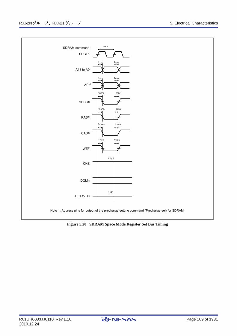
R01UH0033JJ0110 Rev.1.10 Page 109 of 19312010.12.24
RX62Nグループ、RX621グループ 5. Electrical Characteristics
Figure 5.20 SDRAM Space Mode Register Set Bus Timing
A18 to A0
SDCLK
SDCS#
AP*1
DQMn
D31 to D0
RAS#
CAS#
WE#
CKE
SDRAM command
(Hi-Z)
(High)
tCASD
tRASD
tCSD2
t AD2
MRS
t AD2
t AD2
t AD2
tCASD
tRASD
tCSD2
Note 1: Address pins for output of the precharge-setting command (Precharge-sel) for SDRAM.
t WED t WED

R01UH0033JJ0110 Rev.1.10 Page 110 of 19312010.12.24
RX62Nグループ、RX621グループ 5. Electrical Characteristics
Figure 5.21 SDRAM Space Self-Refresh Bus Timing
A18 to A0
(RFS)
SDCLK
SDCS#
AP*1
DQMn
D31 to D0
RAS#
CAS#
WE#
CKE
(Hi-Z)
tCKED
(High)
tCASDtCASDtCASD
tRASD tRASD tRASD
tCSD2tCSD2tCSD2
t AD2
t AD2
(RFA)Ts (RFX) (RFA)
t AD2
t AD2
tCSD2 tCSD2tCSD2t CSD2
tRASD tRASD tRASD tRASD
tCASD tCASD tCASD tCASD
tCKED
Note 1: Address pins for output of the precharge-setting command (Precharge-sel) for SDRAM.
SDRAM command
t DQMD t DQMD
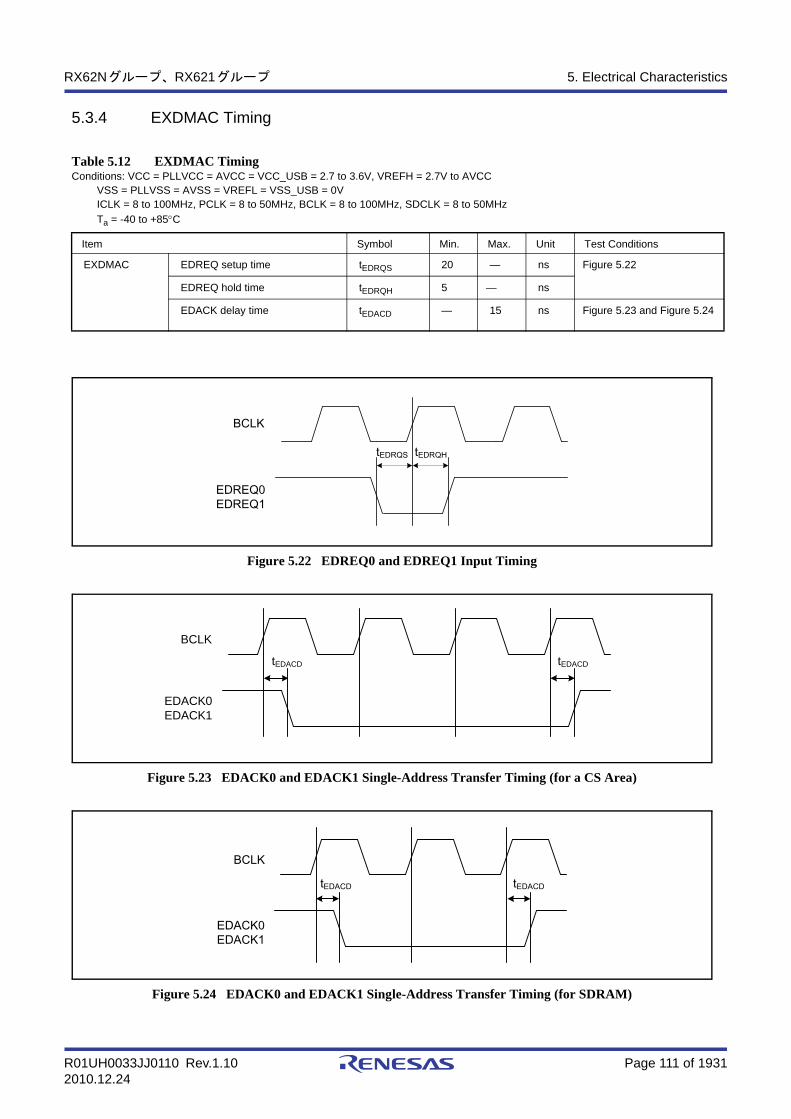
R01UH0033JJ0110 Rev.1.10 Page 111 of 19312010.12.24
RX62Nグループ、RX621グループ 5. Electrical Characteristics
5.3.4 EXDMAC Timing
Figure 5.22 EDREQ0 and EDREQ1 Input Timing
Figure 5.23 EDACK0 and EDACK1 Single-Address Transfer Timing (for a CS Area)
Figure 5.24 EDACK0 and EDACK1 Single-Address Transfer Timing (for SDRAM)
Table 5.12 EXDMAC TimingConditions: VCC = PLLVCC = AVCC = VCC_USB = 2.7 to 3.6V, VREFH = 2.7V to AVCC
VSS = PLLVSS = AVSS = VREFL = VSS_USB = 0VICLK = 8 to 100MHz, PCLK = 8 to 50MHz, BCLK = 8 to 100MHz, SDCLK = 8 to 50MHz
Ta = -40 to +85C
Item Symbol Min. Max. Unit Test Conditions
EXDMAC EDREQ setup time tEDRQS 20 — ns Figure 5.22
EDREQ hold time tEDRQH 5 — ns
EDACK delay time tEDACD — 15 ns Figure 5.23 and Figure 5.24
BCLK
tEDRQS tEDRQH
EDREQ0EDREQ1
EDACK0EDACK1
tEDACD
BCLK
tEDACD
EDACK0EDACK1
tEDACD
BCLK
tEDACD

R01UH0033JJ0110 Rev.1.10 Page 112 of 19312010.12.24
RX62Nグループ、RX621グループ 5. Electrical Characteristics
5.3.5 Timing of On-Chip Peripheral Modules
Table 5.13 Timing of On-Chip Peripheral Modules (1)Conditions: VCC = PLLVCC = AVCC = VCC_USB = 2.7 to 3.6V, VREFH = 2.7V to AVCC
VSS = PLLVSS = AVSS = VREFL = VSS_USB = 0VPCLK = 8 to 50MHz
Ta = -40 to +85C
Item Symbol Min. Max. Unit Test Conditions
I/O ports Output data delay time tPWD — 40 ns Figure 5.25
Input data setup time tPRS 25 — ns
Input data hold time tPRH25 — ns
MTU2 Output compare output delay time tTOCD— 40 ns Figure 5.26
Input capture input setup time tTICS20 — ns
Input capture input pulse width(single-edge setting)
tTICW1.5 × tPcyc — ns
Input capture input pulse width(both-edge setting)
tTICW2.5 × tPcyc — ns
Timer input setup time tTCKS20 — ns Figure 5.27
Timer clock pulse width (single-edge setting)
tTCKWH/L1.5 × tPcyc — ns
Timer clock pulse width (both-edge setting)
tTCKWH/L2.5 × tPcyc — ns
Timer clock pulse width (phase coefficient mode)
tTCKWH/L2.5 × tPcyc — ns
POE2 POE# input setup time tPOES50 — ns Figure 5.28
POE# input pulse width tPOEW1.5 × tPcyc — ns
PPG Pulse output delay time tPOD— 40 ns Figure 5.29
8-bit timer Timer output delay time tTMOD— 40 ns Figure 5.30
Timer reset input setup time tTMRS25 — ns Figure 5.31
Timer clock input setup time tTMCS25 — ns Figure 5.32
Timer clock pulse width
Single-edge setting tTMCWH1.5 × tPcyc — ns
Both-edge setting tTMCWL2.5 × tPcyc — ns
WDT Overflow output delay time tWOVD— 40 ns Figure 5.33

R01UH0033JJ0110 Rev.1.10 Page 113 of 19312010.12.24
RX62Nグループ、RX621グループ 5. Electrical Characteristics
Table 5.13 Timing of On-Chip Peripheral Modules (1) (1/2)Conditions: VCC = PLLVCC = AVCC = VCC_USB = 2.7 to 3.6V, VREFH = 2.7V to AVCC
VSS = PLLVSS = AVSS = VREFL = VSS_USB = 0VPCLK = 8 to 50MHz
Ta = -40 to +85C
Item Symbol Min. Max. Unit Test Conditions
SCI Input clock cycle Asynchronous tScyc4 × tPcyc — ns Figure 5.34 and
Figure 5.35Clock synchronous
6 × tPcyc —
Input clock pulse width tSCKW0.4 × tScyc 0.6 × tScyc ns
Input clock rise time tSCKr— 20 ns
Input clock fall time tSCKf— 20 ns
Output clock cycle Asynchronous tScyc4 × tPcyc — ns
Clock synchronous
6 × tPcyc —
Output clock pulse width tSCKW0.4 × tScyc 0.6 × tScyc ns
Output clock rise time tSCKr— 20 ns
Output clock fall time tSCKf— 20 ns
Transmit data delay time (clock synchronous)
tTXD — 40 ns
Receive data setup time (clock synchronous)
tRXS 40 — ns
Receive data hold time (clock synchronous)
tRXH 40 — ns
A/D converter
10-bit A/D convertertrigger input setup time
tTRGS 25 — ns Figure 5.36
12-bit A/D convertertrigger input setup time
tTRGS 25 — ns
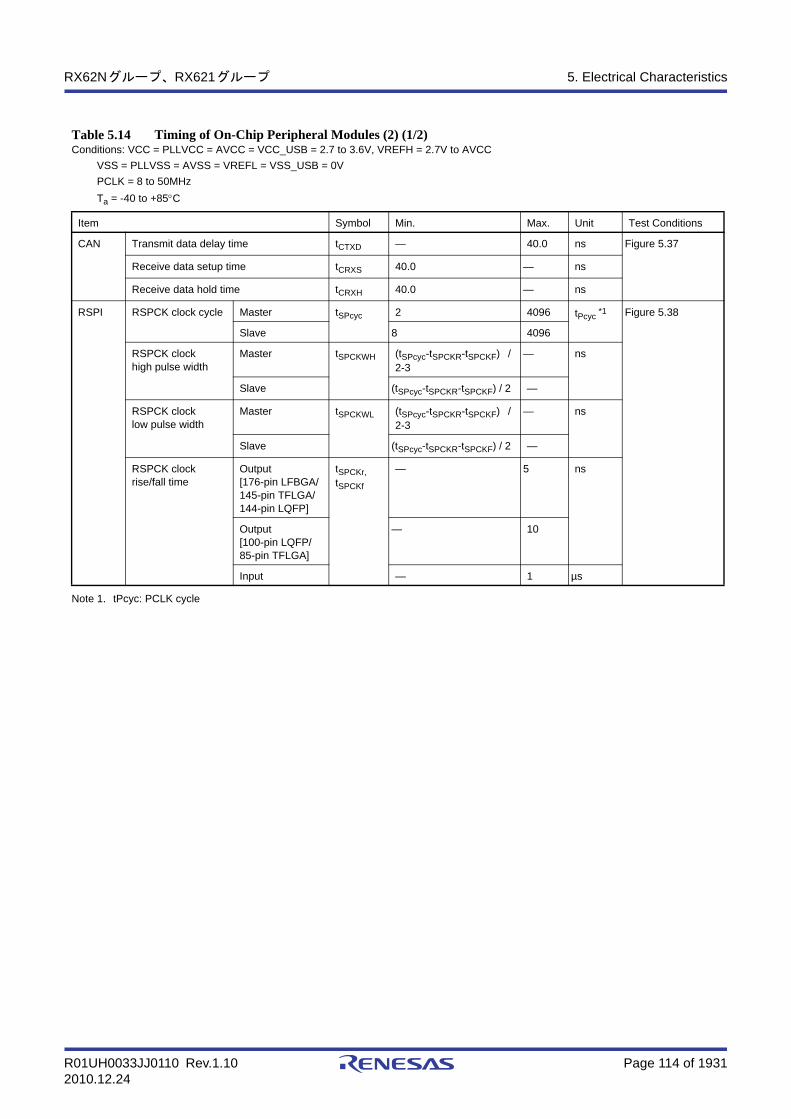
R01UH0033JJ0110 Rev.1.10 Page 114 of 19312010.12.24
RX62Nグループ、RX621グループ 5. Electrical Characteristics
Note 1. tPcyc: PCLK cycle
Table 5.14 Timing of On-Chip Peripheral Modules (2) (1/2)Conditions: VCC = PLLVCC = AVCC = VCC_USB = 2.7 to 3.6V, VREFH = 2.7V to AVCC
VSS = PLLVSS = AVSS = VREFL = VSS_USB = 0V
PCLK = 8 to 50MHz
Ta = -40 to +85C
Item Symbol Min. Max. Unit Test Conditions
CAN Transmit data delay time tCTXD — 40.0 ns Figure 5.37
Receive data setup time tCRXS 40.0 — ns
Receive data hold time tCRXH 40.0 — ns
RSPI RSPCK clock cycle Master tSPcyc 2 4096 tPcyc *1 Figure 5.38
Slave 8 4096
RSPCK clock high pulse width
Master tSPCKWH (tSPcyc-tSPCKR-tSPCKF) /2-3
— ns
Slave (tSPcyc-tSPCKR-tSPCKF) / 2 —
RSPCK clocklow pulse width
Master tSPCKWL (tSPcyc-tSPCKR-tSPCKF) /2-3
— ns
Slave (tSPcyc-tSPCKR-tSPCKF) / 2 —
RSPCK clockrise/fall time
Output[176-pin LFBGA/145-pin TFLGA/144-pin LQFP]
tSPCKr, tSPCKf
— 5 ns
Output[100-pin LQFP/85-pin TFLGA]
— 10
Input — 1 µs

R01UH0033JJ0110 Rev.1.10 Page 115 of 19312010.12.24
RX62Nグループ、RX621グループ 5. Electrical Characteristics
Note 1. tPcyc: PCLK cycle
Table 5.14 Timing of On-Chip Peripheral Modules (2) (2/2)Conditions: VCC = PLLVCC = AVCC = VCC_USB = 2.7 to 3.6V, VREFH = 2.7V to AVCC
VSS = PLLVSS = AVSS = VREFL = VSS_USB = 0VPCLK = 8 to 50MHz
Ta = -40 to +85C
Item Symbol Min. Max. Unit Test Conditions
RSPI Data input setup time Master[176-pin LFBGA/145-pin TFLGA/144-pin LQFP]
tSU 16 — ns Figure 5.39 to Figure 5.42
Master[100-pin LQFP/85-pin TFLGA]
30 —
Slave 20-2 × tPcyc —
Data input hold time Master tH 0 — ns
Slave 20+2 × tPcyc —
SSL setup time Master tLEAD 1 8 tSPcyc
Slave 4 — tPcyc
SSL hold time Master tLAG 1 8 tSPcyc
Slave 4 — tPcyc
Data output delay time Master[176-pin LFBGA/145-pin TFLGA/144-pin LQFP]
tOD — 20 ns
Master[100-pin LQFP/85-pin TFLGA]
— 30
Slave[176-pin LFBGA/145-pin TFLGA/144-pin LQFP]
— 3 × tPcyc+40
Slave[100-pin LQFP/85-pin TFLGA]
— 3 × tPcyc+50

R01UH0033JJ0110 Rev.1.10 Page 116 of 19312010.12.24
RX62Nグループ、RX621グループ 5. Electrical Characteristics
Note 1. tPcyc: PCLK cycle
Table 5.15 Timing of On-Chip Peripheral Modules (3)Conditions: VCC = PLLVCC = AVCC = VCC_USB = 2.7 to 3.6V, VREFH = 2.7V to AVCC
VSS = PLLVSS = AVSS = VREFL = VSS_USB = 0VPCLK = 8 to 50MHz
Ta = -40 to +85C
Item Symbol Min. Max. Unit Test Conditions
RSPI Data output hold time Master tOH 0 — ns Figure 5.39 to Figure 5.42
Slave 0 —
Sucessive transmission delay time
Master tTD tSPcyc+2 × tPcyc 8 × tSPcyc+2 × tPcyc
ns
Slave 4 × tPcyc —
MOSI, MISO rise/fall time Output[176-pin LFBGA/145-pin TFLGA/144-pin LQFP]
tDr, tDf
— 5 ns
Output[100-pin LQFP/85-pin TFLGA]
— 10
Input — 1 µs
SSL rise/fall time Output[176-pin LFBGA145-pin TFLGA144-pin LQFP]
tSSLr, tSSLf
— 5 ns
Output[100-pin LQFP/85-pin TFLGA]
— 10
Input — 1 µs
Slave access time tSA — 4 tPcyc Figure 5.41 and Figure 5.42
Slave output release tim tREL — 3 tPcyc
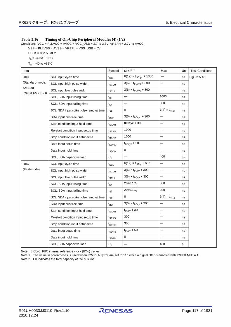
R01UH0033JJ0110 Rev.1.10 Page 117 of 19312010.12.24
RX62Nグループ、RX621グループ 5. Electrical Characteristics
Note: tIICcyc: RIIC internal reference clock (IICφ) cyclesNote 1. The value in parentheses is used when ICMR3.NF[1:0] are set to 11b while a digital filter is enabled with ICFER.NFE = 1.Note 2. Cb indicates the total capacity of the bus line.
Table 5.16 Timing of On-Chip Peripheral Modules (4) (1/2)Conditions: VCC = PLLVCC = AVCC = VCC_USB = 2.7 to 3.6V, VREFH = 2.7V to AVCC
VSS = PLLVSS = AVSS = VREFL = VSS_USB = 0V
PCLK = 8 to 50MHz
Ta = -40 to +85C
Ta = -40 to +85C
Item Symbol Min.*1*2 Max. Unit Test Conditions
RIIC
(Standard-mode,
SMBus)
ICFER.FMPE = 0
SCL input cycle time tSCL6(12) × tIICcyc + 1300 — ns Figure 5.43
SCL input high pulse width tSCLH3(6) × tIICcyc + 300 — ns
SCL input low pulse width tSCLL3(6) × tIICcyc + 300 — ns
SCL, SDA input rising time tSr— 1000 ns
SCL, SDA input falling time tSf— 300 ns
SCL, SDA input spike pulse removal time tSP0 1(4) × tIICcy ns
SDA input bus free time tBUF3(6) × tIICcyc + 300 — ns
Start condition input hold time tSTAHtIICcyc + 300 — ns
Re-start condition input setup time tSTAS1000 — ns
Stop condition input setup time tSTOS1000 — ns
Data input setup time tSDAStIICcyc + 50 — ns
Data input hold time tSDAH0 — ns
SCL, SDA capacitive load Cb— 400 pF
RIIC
(Fast-mode)
SCL input cycle time tSCL6(12) × tIICcy + 600 — ns
SCL input high pulse width tSCLH3(6) × tIICcy + 300 — ns
SCL input low pulse width tSCLL3(6) × tIICcy + 300 — ns
SCL, SDA input rising time tSr20+0.1Cb 300 ns
SCL, SDA input falling time tSf20+0.1Cb 300 ns
SCL, SDA input spike pulse removal time tSP0 1(4) × tIICcy ns
SDA input bus free time tBUF3(6) × tIICcy + 300 — ns
Start condition input hold time tSTAHtIICcy + 300 — ns
Re-start condition input setup time tSTAS300 — ns
Stop condition input setup time tSTOS300 — ns
Data input setup time tSDAStIICcy + 50 — ns
Data input hold time tSDAH0 — ns
SCL, SDA capacitive load Cb — 400 pF

R01UH0033JJ0110 Rev.1.10 Page 118 of 19312010.12.24
RX62Nグループ、RX621グループ 5. Electrical Characteristics
Note: tIICcyc: RIIC internal reference clock (IICφ) cyclesNote 1. The value in parentheses is used when ICMR3.NF[1:0] are set to 11b while a digital filter is enabled with ICFER.NFE = 1.Note 2. Cb indicates the total capacity of the bus line.
Table 5.16 Timing of On-Chip Peripheral Modules (4) (2/2)Conditions: VCC = PLLVCC = AVCC = VCC_USB = 2.7 to 3.6V, VREFH = 2.7V to AVCC
VSS = PLLVSS = AVSS = VREFL = VSS_USB = 0V
PCLK = 8 to 50MHz
Ta = -40 to +85Cz
Ta = -40 to +85C
Item Symbol Min.*1*2 Max. Unit Test Conditions
RIIC
(Fast-mode+)
ICFER.FMPE = 1
SCL input cycle time tSCL6(12) × tIICcyc + 240 — ns Figure 5.43
SCL input high pulse width tSCLH3(6) × tIICcyc + 120 — ns
SCL input low pulse width tSCLL3(6) × tIICcyc + 120 — ns
SCL, SDA input rising time tSr— 120 ns
SCL, SDA input falling time tSf— 120 ns
SCL, SDA input spike pulse removal time tSP0 1(4) × tIICcyc ns
SDA input bus free time tBUF3(6) × tIICcyc + 120 — ns
Start condition input hold time tSTAHtIICcyc + 120 ns
Re-start condition input setup time tSTAS120 — ns
Stop condition input setup time tSTOS120 — ns
Data input setup time tSDAStIICcyc + 20 — ns
Data input hold time tSDAH 0 — ns
SCL, SDA capacitive load Cb — 550 pF
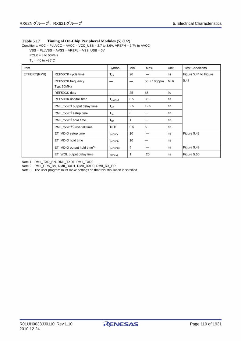
R01UH0033JJ0110 Rev.1.10 Page 119 of 19312010.12.24
RX62Nグループ、RX621グループ 5. Electrical Characteristics
Note 1. RMII_TXD_EN, RMII_TXD1, RMII_TXD0Note 2. RMII_CRS_DV, RMII_RXD1, RMII_RXD0, RMII_RX_ERNote 3. The user program must make settings so that this stipulation is satisfied.
Table 5.17 Timing of On-Chip Peripheral Modules (5) (1/2)Conditions: VCC = PLLVCC = AVCC = VCC_USB = 2.7 to 3.6V, VREFH = 2.7V to AVCC
VSS = PLLVSS = AVSS = VREFL = VSS_USB = 0V
PCLK = 8 to 50MHz
Ta = -40 to +85C
Item Symbol Min. Max. Unit Test Conditions
ETHERC(RMII) REF50CK cycle time Tck 20 — ns Figure 5.44 to Figure
5.47REF50CK frequency
Typ. 50MHz
— — 50 + 100ppm MHz
REF50CK duty — 35 65 %
REF50CK rise/fall time Tckr/ckf 0.5 3.5 ns
RMII_xxxx*1 output delay time Tco 2.5 12.5 ns
RMII_xxxx*2 setup time Tsu 3 — ns
RMII_xxxx*2 hold time Thd 1 — ns
RMII_xxxx*1*2 rise/fall time Tr/Tf 0.5 6 ns
ET_MDIO setup time tMDIOs 10 — ns Figure 5.48
ET_MDIO hold time tMDIOh 10 — ns
ET_MDIO output hold time*3 tMDIODh 5 — ns Figure 5.49
ET_WOL output delay time tWOLd 1 20 ns Figure 5.50

R01UH0033JJ0110 Rev.1.10 Page 120 of 19312010.12.24
RX62Nグループ、RX621グループ 5. Electrical Characteristics
Note 1. RMII_TXD_EN, RMII_TXD1, RMII_TXD0Note 2. RMII_CRS_DV, RMII_RXD1, RMII_RXD0, RMII_RX_ERNote 3. The user program must make settings so that this stipulation is satisfied.
Table 5.17 Timing of On-Chip Peripheral Modules (5) (2/2)Conditions: VCC = PLLVCC = AVCC = VCC_USB = 2.7 to 3.6V, VREFH = 2.7V to AVCC
VSS = PLLVSS = AVSS = VREFL = VSS_USB = 0V
PCLK = 8 to 50MHz
Ta = -40 to +85C
Item Symbol Min. Max. Unit Test Conditions
ETHERC(MII) ET_TX_CLK cycle time tTcyc 40 — ns —
ET_TX_EN output delay time tTENd 1 20 ns Figure 5.51
ET_ETXD0 to ET_ETXD3 output delay time tMTDd 1 20 ns
ET_CRS setup time tCRSs 10 — ns
ET_CRS hold time tCRSh 10 — ns
ET_COL setup time tCOLs 10 — ns Figure 5.52
ET_COL hold time tCOLh 10 — ns
ET_RX_CLK cycle time tTRcyc 40 — ns —
ET_RX_DV setup time tRDVs 10 ns Figure 5.53
ET_RX_DV hold time tRDVh 10 — ns
ET_ERXD0 to ET_ERXD3 setup time tMRDs 10 — ns
ET_ERXD0 to ET_ERXD3 hold time tMRDh 10 — ns
ET_RX_ER setup time tRERs 10 — ns Figure 5.54
ET_RX_ER hold time tRESh 10 — ns
ET_MDIO setup time tMDIOs 10 — ns Figure 5.55
ET_MDIO hold time tMDIOh 10 — ns
ET_MDIO utput hold time tMDIOdh 5 — ns Figure 5.56
ET_WOL output delay time tWOLd 1 20 ns Figure 5.57

R01UH0033JJ0110 Rev.1.10 Page 121 of 19312010.12.24
RX62Nグループ、RX621グループ 5. Electrical Characteristics
Figure 5.25 I/O Port Input/Output Timing
Figure 5.26 MTU2 Input/Output Timing
Table 5.18 Timing of On-Chip Peripheral Modules (6)Conditions: VCC = PLLVCC = AVCC = VCC_USB = 2.7 to 3.6V, VREFH = 2.7V to AVCC
VSS = PLLVSS = AVSS = VREFL = VSS_USB = 0V
PCLK = 8 to 50MHz
Ta = -40 to +85C
Item Symbol Min. Typ. Max. Unit Test Conditions
TCK clock cycle time tTCKcyc 100 — — ns Figure 5.58
TCK clock high pulse width tTCKH 45 — — ns
TCK clock low pulse width tTCKL 45 — — ns
TCK clock rising time tTCKr — — 5 ns
TCK clock falling time tTCKf — — 5 ns
TRST# pulse width tTRSTW 20 — — tTCKcyc Figure 5.59
TMS setup time tTMSS 20 — — ns Figure 5.60
TMS hold time tTMSH 20 — — ns
TDI setup time tTDIS 20 — — ns
TDI hold time tTDIH 20 — — ns
TDO data delay time tTDOD — — 40 ns
PCLK
T1
tPRS
T2
tPRH
tPWD
Input port (read)
Output port (write)
Output compare output
Input capture input
PCLK
tTOCD
tTICS
tTICW

R01UH0033JJ0110 Rev.1.10 Page 122 of 19312010.12.24
RX62Nグループ、RX621グループ 5. Electrical Characteristics
Figure 5.27 MTU2 Clock Input Timing
Figure 5.28 POE# Input Timing
Figure 5.29 PPG Output Timing
Figure 5.30 8-Bit Timer Output Timing
MTCLKA to MTCLKH
PCLK
tTCKWL tTCKWH
tTCKS tTCKS
POEn# input
PCLK
tPOES
tPOEW
PCLK
PO31 to PO0
tPOD
PCLK
TMO0 to TMO3
tTMOD

R01UH0033JJ0110 Rev.1.10 Page 123 of 19312010.12.24
RX62Nグループ、RX621グループ 5. Electrical Characteristics
Figure 5.31 8-Bit Timer Reset Input Timing
Figure 5.32 8-Bit Timer Clock Input Timing
Figure 5.33 WDT Output Timing
Figure 5.34 SCK Clock Input Timing
PCLK
TMRI0 to TMRI3
tTMRS
PCLK
TMCI0 to TMCI3
tTMCS tTMCS
tTMCWL tTMCWH
PCLK
WDTOVF#
tWOVDtWOVD
tSCKW tSCKr tSCKf
tScyc
SCKn(n = 0 to 3, 5, 6)

R01UH0033JJ0110 Rev.1.10 Page 124 of 19312010.12.24
RX62Nグループ、RX621グループ 5. Electrical Characteristics
Figure 5.35 SCI Input/Output Timing: Clock Synchronous Mode
Figure 5.36 A/D Converter External Trigger Input Timing
Figure 5.37 CAN Input/Output Timing
tTXD
tRXS tRXH
TxDn
RxDn
SCKn
n = 0 to 3, 5, 6
tTRGS
ADTRG0#-A/BADTRG1#
PCLK
PCLK
tCRXS
CRX0
CTX0
tCRXH
tCTXD
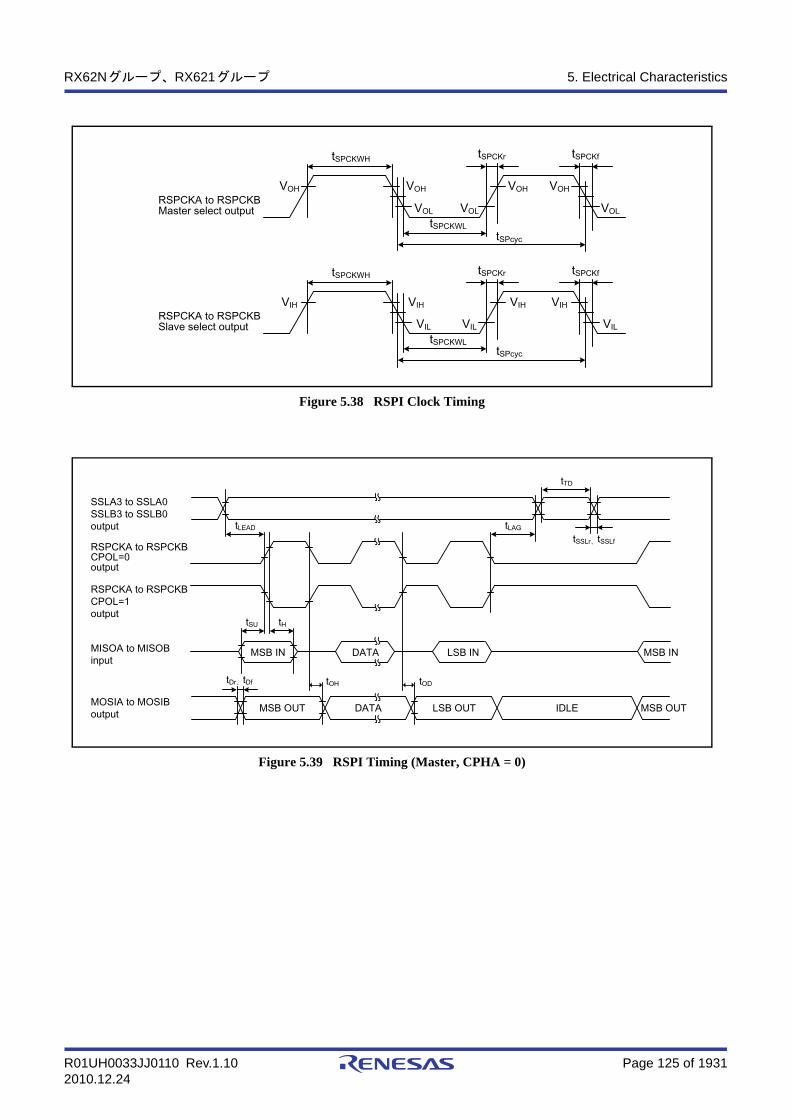
R01UH0033JJ0110 Rev.1.10 Page 125 of 19312010.12.24
RX62Nグループ、RX621グループ 5. Electrical Characteristics
Figure 5.38 RSPI Clock Timing
Figure 5.39 RSPI Timing (Master, CPHA = 0)
RSPCKA to RSPCKBMaster select output
RSPCKA to RSPCKBSlave select output
tSPCKWH
VOH VOH
VOL VOL
VOH VOH
tSPCKWL
tSPCKr tSPCKf
VOL
tSPcyc
tSPCKWH
VIH VIH
VIL VIL
VIH VIH
tSPCKWL
tSPCKr tSPCKf
VIL
tSPcyc
SSLA3 to SSLA0SSLB3 to SSLB0output
RSPCKA to RSPCKBCPOL=0output
RSPCKA to RSPCKBCPOL=1output
MISOA to MISOBinput
MOSIA to MOSIBoutput
tDr、tDf
tSU tH
tLEAD
tTD
tLAG
tSSLr、tSSLf
tOH tOD
MSB IN DATA LSB IN MSB IN
MSB OUT DATA LSB OUT IDLE MSB OUT

R01UH0033JJ0110 Rev.1.10 Page 126 of 19312010.12.24
RX62Nグループ、RX621グループ 5. Electrical Characteristics
Figure 5.40 RSPI Timing (Master, CPHA = 1)
Figure 5.41 RSPI Timing (Slave, CPHA = 0)
SSLA3 to SSLA0SSLB3 to SSLB0output
RSPCKA to RSPCKBCPOL=0output
RSPCKA to RSPCKBCPOL=1output
MISOA to MISOBinput
MOSIA to MOSIBoutput
tDr、tDf
tSU tH
tLEAD
tTD
tLAG
tSSLr、tSSLf
tOH
MSB IN DATA LSB IN MSB IN
MSB OUT DATA LSB OUT IDLE MSB OUT
tOD
SSLA0SSLB0input
RSPCKA to RSPCKBCPOL=0input
RSPCKA to RSPCKBCPOL=1input
MOSIA to MOSIBinput
MISOA to MISOBoutput
tDr、tDftSU tH
tLEAD
tTD
tLAG
tSA
MSB IN DATA LSB IN MSB IN
MSB OUT DATA LSB OUT MSB IN MSB OUT
tOH tOD tREL
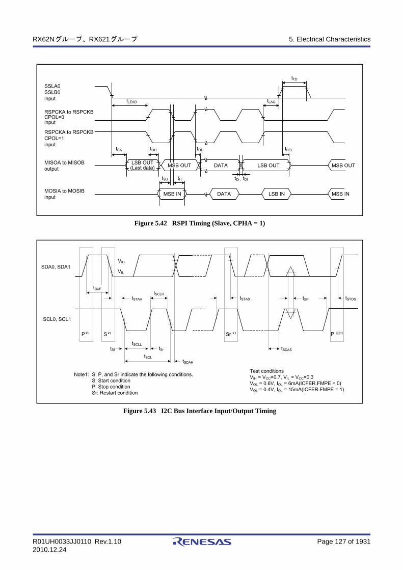
R01UH0033JJ0110 Rev.1.10 Page 127 of 19312010.12.24
RX62Nグループ、RX621グループ 5. Electrical Characteristics
Figure 5.42 RSPI Timing (Slave, CPHA = 1)
Figure 5.43 I2C Bus Interface Input/Output Timing
SSLA0SSLB0input
RSPCKA to RSPCKBCPOL=0input
RSPCKA to RSPCKBCPOL=1input
MISOA to MISOBoutput
MOSIA to MOSIBinput
tDr、tDf
tSA tOH
tLEAD
tTD
tLAG
tH
LSB OUT(Last data) DATA MSB OUT
MSB IN DATA LSB IN MSB IN
LSB OUT
tSU
tOD tREL
MSB OUT
SDA0, SDA1
SCL0, SCL1
VIH
VIL
tSTAHtSCLH
tSCLL
P *1 S *1
tSf tSr
tSCLtSDAH
tSDAS
tSTAS tSP tSTOS
P(注1)
tBUF
Note1: S, P, and Sr indicate the following conditions.S: Start conditionP: Stop conditionSr: Restart condition
Test conditionsVIH = VCC×0.7, VIL = VCC×0.3VOL = 0.6V, IOL = 6mA(ICFER.FMPE = 0)VOL = 0.4V, IOL = 15mA(ICFER.FMPE = 1)
Sr *1

R01UH0033JJ0110 Rev.1.10 Page 128 of 19312010.12.24
RX62Nグループ、RX621グループ 5. Electrical Characteristics
Figure 5.44 REF50CK and RMII Signal Timing
Figure 5.45 RMII Transmission Timing
Figure 5.46 RMII Reception Timing (Normal Operation)
Tck
REF50CK
Tckr
Tckf
Tco Tsu Thd
SignalSignal Signal transitions
Signal transitions
Signal transitions
TfTr
90%
50%
10%
90%
50%
10%
RMII_xxxx *1
Note1. RMII_TXD_EN、RMII_TXD1、RMII_TXD0、RMII_CRS_DV、RMII_RXD1、RMII_RXD0、RMII_RX_ER
Tck
Tco
DATA
Tco
SFD CRCRMII_TXD1RMII_TXD0
RMII_TXD_EN
REF50CK
Preamble
DATA
SFD
CRCPreamble
Thd
TsuRMII_RXD1RMII_RXD0
RMII_RX_ER
RMII_CRS_DV
REF50CK
L
ThdTsu

R01UH0033JJ0110 Rev.1.10 Page 129 of 19312010.12.24
RX62Nグループ、RX621グループ 5. Electrical Characteristics
Figure 5.47 RMII Reception Timing (Error Occurrence)
Figure 5.48 MDIO Input Timing (RMII)
Figure 5.49 MDIO Output Timing (RMII)
Figure 5.50 WOL Output Timing (RMII)
DATASFD xxxxPreamble
REF50CK
Tsu
RMII_RXD1RMII_RXD0
RMII_RX_ER
RMII_CRS_DV
Thd
ET_MDC
ET_MDIO
tMDIOhtMDIOs
ET_MDC
ET_MDIO
tMDIOdh
ET_WOL
tWOLd
REF50CK
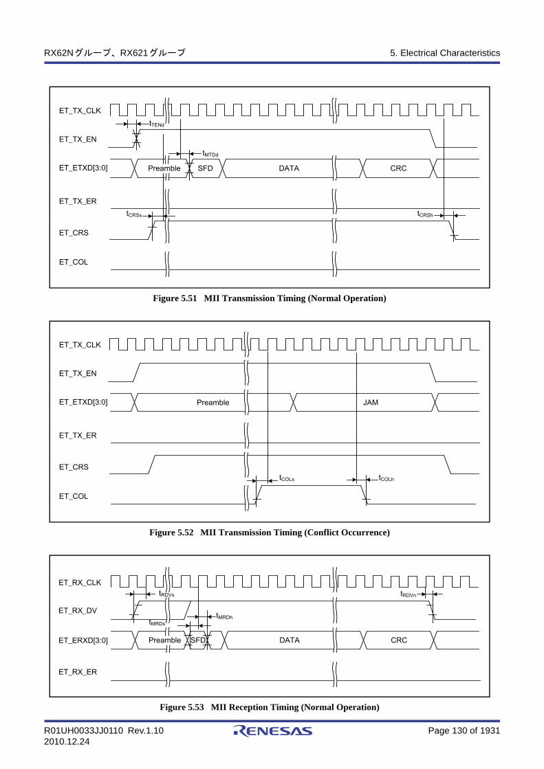
R01UH0033JJ0110 Rev.1.10 Page 130 of 19312010.12.24
RX62Nグループ、RX621グループ 5. Electrical Characteristics
Figure 5.51 MII Transmission Timing (Normal Operation)
Figure 5.52 MII Transmission Timing (Conflict Occurrence)
Figure 5.53 MII Reception Timing (Normal Operation)
DATASFD CRC
tMTDd
tTENd
tCRSs tCRSh
Preamble
ET_COL
ET_CRS
ET_TX_ER
ET_ETXD[3:0]
ET_TX_EN
ET_TX_CLK
JAM
tCOLh
Preamble
ET_COL
ET_CRS
ET_TX_ER
ET_ETXD[3:0]
ET_TX_EN
ET_TX_CLK
tCOLs
DATASFD CRC
tMRDh
Preamble
ET_RX_ER
tRDVs
tMRDs
tRDVn
ET_ERXD[3:0]
ET_RX_DV
ET_RX_CLK

R01UH0033JJ0110 Rev.1.10 Page 131 of 19312010.12.24
RX62Nグループ、RX621グループ 5. Electrical Characteristics
Figure 5.54 MII Reception Timing (Error Occurrence)
Figure 5.55 MDIO Input Timing (MII)
Figure 5.56 MDIO Output Timing(MII)
Figure 5.57 WOL Output Timing(MII)
DATASFD XXXXtRERh
Preamble
ET_RX_ER
ET_ERXD[3:0]
ET_RX_DV
ET_RX_CLK
tRERs
ET_MDC
ET_MDIO
tMDIOhtMDIOs
ET_MDC
ET_MDIO
tMDIOdh
ET_RX_CLK
ET_WOL
tWOLd

R01UH0033JJ0110 Rev.1.10 Page 132 of 19312010.12.24
RX62Nグループ、RX621グループ 5. Electrical Characteristics
Figure 5.58 Boundary Scan TCK Timing
Figure 5.59 Boundary Scan TRST# Timing
Figure 5.60 Boundary Scan Input/Output Timing
TCK
tTCKcyc
tTCKH
tTCKf
tTCKL tTCKr
RES#
TRST#
TCK
tTRSTW
tTMSS
TCK
TMS
TDI
TDO
tTMSH
tTDIS tTDIH
tTDOD
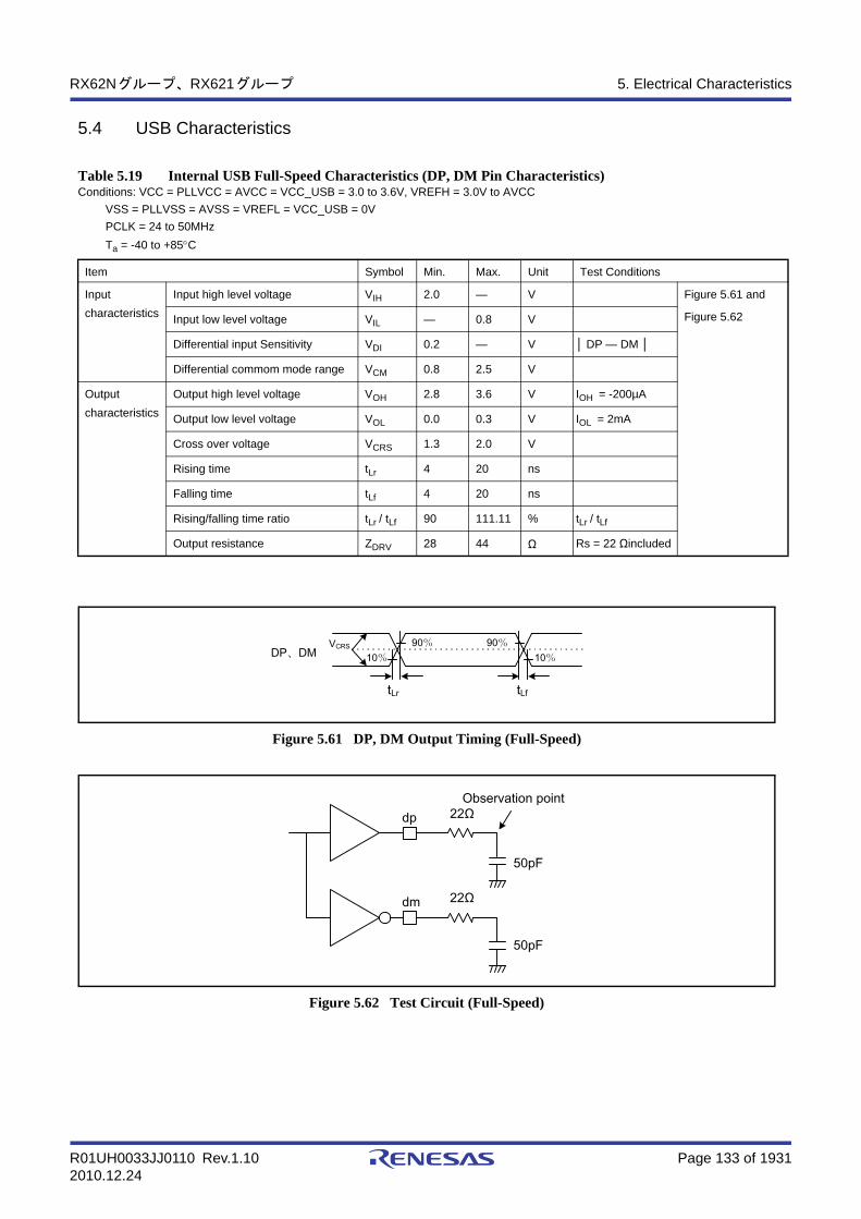
R01UH0033JJ0110 Rev.1.10 Page 133 of 19312010.12.24
RX62Nグループ、RX621グループ 5. Electrical Characteristics
5.4 USB Characteristics
Figure 5.61 DP, DM Output Timing (Full-Speed)
Figure 5.62 Test Circuit (Full-Speed)
Table 5.19 Internal USB Full-Speed Characteristics (DP, DM Pin Characteristics)Conditions: VCC = PLLVCC = AVCC = VCC_USB = 3.0 to 3.6V, VREFH = 3.0V to AVCC
VSS = PLLVSS = AVSS = VREFL = VCC_USB = 0V
PCLK = 24 to 50MHz
Ta = -40 to +85C
Item Symbol Min. Max. Unit Test Conditions
Input
characteristics
Input high level voltage VIH 2.0 — V Figure 5.61 and
Figure 5.62Input low level voltage VIL — 0.8 V
Differential input Sensitivity VDI 0.2 — V DP — DM
Differential commom mode range VCM 0.8 2.5 V
Output
characteristics
Output high level voltage VOH 2.8 3.6 V IOH = -200µA
Output low level voltage VOL 0.0 0.3 V IOL = 2mA
Cross over voltage VCRS 1.3 2.0 V
Rising time tLr 4 20 ns
Falling time tLf 4 20 ns
Rising/falling time ratio tLr / tLf 90 111.11 % tLr / tLf
Output resistance ZDRV 28 44 Ω Rs = 22 Ωincluded
DP、DM
tLftLr
90%10%10%
90%VCRS
Observation point22Ω
22Ω
50pF
50pF
dp
dm
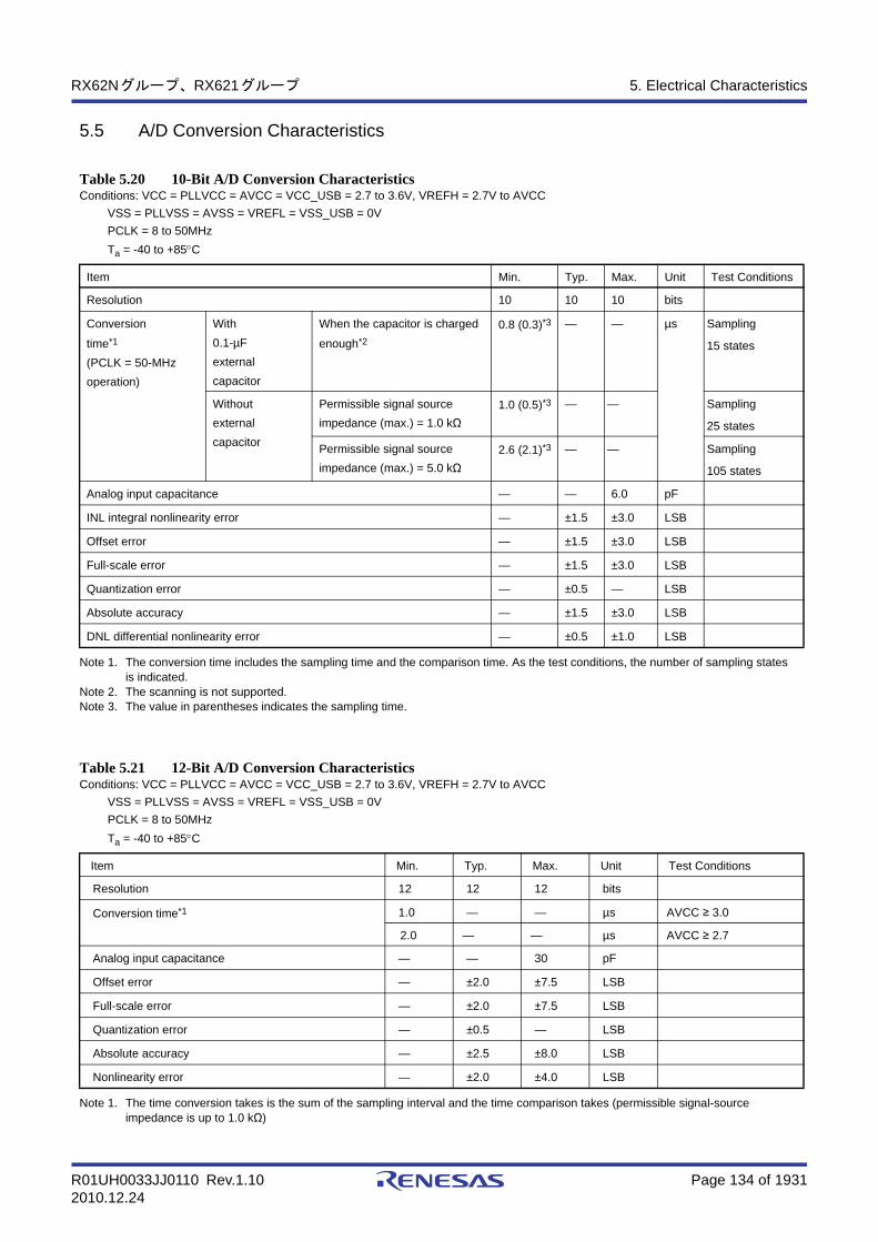
R01UH0033JJ0110 Rev.1.10 Page 134 of 19312010.12.24
RX62Nグループ、RX621グループ 5. Electrical Characteristics
5.5 A/D Conversion Characteristics
Note 1. The conversion time includes the sampling time and the comparison time. As the test conditions, the number of sampling states is indicated.
Note 2. The scanning is not supported.Note 3. The value in parentheses indicates the sampling time.
Note 1. The time conversion takes is the sum of the sampling interval and the time comparison takes (permissible signal-source impedance is up to 1.0 kΩ)
Table 5.20 10-Bit A/D Conversion CharacteristicsConditions: VCC = PLLVCC = AVCC = VCC_USB = 2.7 to 3.6V, VREFH = 2.7V to AVCC
VSS = PLLVSS = AVSS = VREFL = VSS_USB = 0V
PCLK = 8 to 50MHz
Ta = -40 to +85C
Item Min. Typ. Max. Unit Test Conditions
Resolution 10 10 10 bits
Conversion
time*1
(PCLK = 50-MHz
operation)
With
0.1-µF
external
capacitor
When the capacitor is charged
enough*2
0.8 (0.3)*3 — — µs Sampling
15 states
Without
external
capacitor
Permissible signal source
impedance (max.) = 1.0 kΩ
1.0 (0.5)*3 — — Sampling
25 states
Permissible signal source
impedance (max.) = 5.0 kΩ
2.6 (2.1)*3 — — Sampling
105 states
Analog input capacitance — — 6.0 pF
INL integral nonlinearity error — ±1.5 ±3.0 LSB
Offset error — ±1.5 ±3.0 LSB
Full-scale error — ±1.5 ±3.0 LSB
Quantization error — ±0.5 — LSB
Absolute accuracy — ±1.5 ±3.0 LSB
DNL differential nonlinearity error — ±0.5 ±1.0 LSB
Table 5.21 12-Bit A/D Conversion CharacteristicsConditions: VCC = PLLVCC = AVCC = VCC_USB = 2.7 to 3.6V, VREFH = 2.7V to AVCC
VSS = PLLVSS = AVSS = VREFL = VSS_USB = 0V
PCLK = 8 to 50MHz
Ta = -40 to +85C
Item Min. Typ. Max. Unit Test Conditions
Resolution 12 12 12 bits
Conversion time*1 1.0 — — µs AVCC ≥ 3.0
2.0 — — µs AVCC ≥ 2.7
Analog input capacitance — — 30 pF
Offset error — ±2.0 ±7.5 LSB
Full-scale error — ±2.0 ±7.5 LSB
Quantization error — ±0.5 — LSB
Absolute accuracy — ±2.5 ±8.0 LSB
Nonlinearity error — ±2.0 ±4.0 LSB
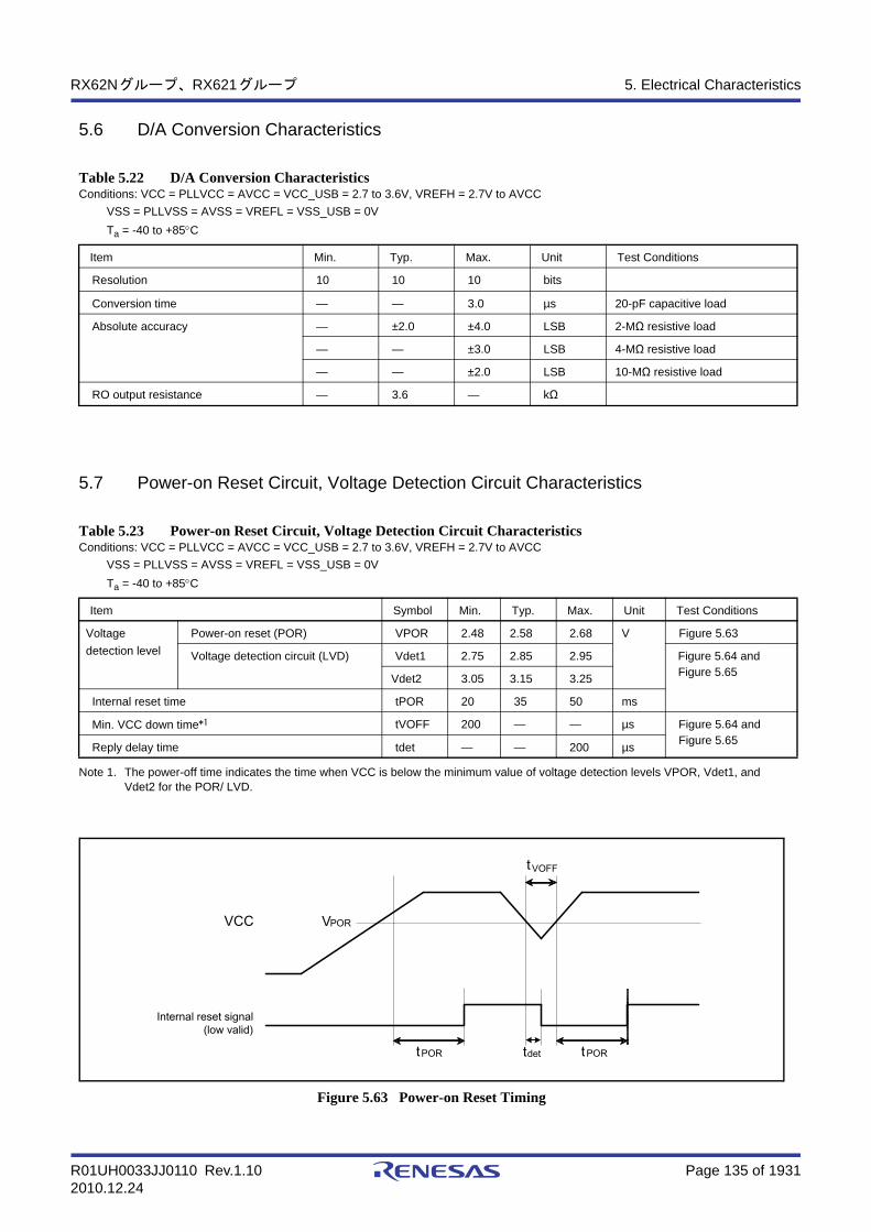
R01UH0033JJ0110 Rev.1.10 Page 135 of 19312010.12.24
RX62Nグループ、RX621グループ 5. Electrical Characteristics
5.6 D/A Conversion Characteristics
5.7 Power-on Reset Circuit, Voltage Detection Circuit Characteristics
Note 1. The power-off time indicates the time when VCC is below the minimum value of voltage detection levels VPOR, Vdet1, and Vdet2 for the POR/ LVD.
Figure 5.63 Power-on Reset Timing
Table 5.22 D/A Conversion CharacteristicsConditions: VCC = PLLVCC = AVCC = VCC_USB = 2.7 to 3.6V, VREFH = 2.7V to AVCC
VSS = PLLVSS = AVSS = VREFL = VSS_USB = 0V
Ta = -40 to +85C
Item Min. Typ. Max. Unit Test Conditions
Resolution 10 10 10 bits
Conversion time — — 3.0 µs 20-pF capacitive load
Absolute accuracy — ±2.0 ±4.0 LSB 2-MΩ resistive load
— — ±3.0 LSB 4-MΩ resistive load
— — ±2.0 LSB 10-MΩ resistive load
RO output resistance — 3.6 — kΩ
Table 5.23 Power-on Reset Circuit, Voltage Detection Circuit CharacteristicsConditions: VCC = PLLVCC = AVCC = VCC_USB = 2.7 to 3.6V, VREFH = 2.7V to AVCC
VSS = PLLVSS = AVSS = VREFL = VSS_USB = 0V
Ta = -40 to +85C
Item Symbol Min. Typ. Max. Unit Test Conditions
Voltage
detection level
Power-on reset (POR) VPOR 2.48 2.58 2.68 V Figure 5.63
Voltage detection circuit (LVD) Vdet1 2.75 2.85 2.95 Figure 5.64 and Figure 5.65
Vdet2 3.05 3.15 3.25
Internal reset time tPOR 20 35 50 ms
Min. VCC down time*1 tVOFF 200 — — µs Figure 5.64 and Figure 5.65
Reply delay time tdet — — 200 µs
Internal reset signal (low valid)
VCC
tVOFF
VPOR
tPORtPOR tdet
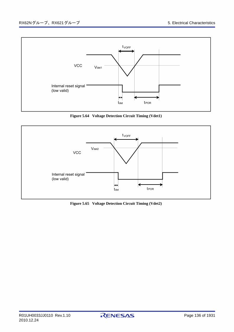
R01UH0033JJ0110 Rev.1.10 Page 136 of 19312010.12.24
RX62Nグループ、RX621グループ 5. Electrical Characteristics
Figure 5.64 Voltage Detection Circuit Timing (Vdet1)
Figure 5.65 Voltage Detection Circuit Timing (Vdet2)
VCC Vdet1
tVOFF
tPORtdet
Internal reset signal (low valid)
VCCVdet2
tVOFF
tPORtdet
Internal reset signal (low valid)

R01UH0033JJ0110 Rev.1.10 Page 137 of 19312010.12.24
RX62Nグループ、RX621グループ 5. Electrical Characteristics
5.8 Oscillation Stop Detection Timing
Figure 5.66 Oscillation Stop Detection Timing
Table 5.24 Oscillation Stop Detection Circuit CharacteristicsConditions: VCC = PLLVCC = AVCC = VCC_USB = 2.7 to 3.6V, VREFH = 2.7V to AVCC
VSS = PLLVSS = AVSS = VREFL = VSS_USB = 0V
Ta = -40 to +85C
Item Symbol Min. Typ. Max. Unit Test Conditions
Detection time tdr — — 1.0 ms Figure 5.66
Internal oscillation frequency when oscillation
stop is detected
fMAIN 0.5 — 7.0 MHz
ICLK
Main clock oscillator
Internal oscillation
Nomal operation Abnomal operationOSTDF*
Note : * This indicates the OSTDF flag in the oscillation detection control register (OSTDCR).
tdr

R01UH0033JJ0110 Rev.1.10 Page 138 of 19312010.12.24
RX62Nグループ、RX621グループ 5. Electrical Characteristics
5.9 ROM (Flash Memory for Code Storage) Characteristics
Note 1. Definition of rewrite/erase cycle:The rewrite/erase cycle is the number of erasing for each block. When the rewrite/erase cycle is n times (n = 1000), erasing can be performed n times for each block. For instance, when 256-byte writing is performed 16 times for different addresses in 4-Kbyte block and then the entire block is erased, the rewrite/erase cycle is counted as one. However, writing to the same address for several times as one erasing is not enabled (over writing is prohibited).
Note 2. This indicates the minimum number that guarantees the characteristics after rewriting. (The guaranteed value is in the range from one to the minimum number.)
Note 3. This indicates the characteristic when rewrite is performed within the specification range including the minimum number.
Table 5.25 ROM (Flash Memory for Code Storage) CharacteristicsConditions: VCC = PLLVCC = AVCC = VCC_USB = 2.7 to 3.6V, VREFH = 2.7V to AVCC
VSS = PLLVSS = AVSS = VREFL = VSS_USB = 0V
Temperature range for the programming/erasure operation: Ta = -40 to +85C
Item Symbol Min. Typ. Max. Unit Test Conditions
Programming time 256 bytes tP256 — 2 12 ms PCLK = 50MHz
NPEC ≤ 1004 Kbytes tP4K — 23 50 ms
16 Kbytes tP16K — 90 200 ms
256 byte tP256 — 2.4 14.4 ms PCLK = 50MHz
NPEC > 1004 Kbytes tP4K — 27.6 60 ms
16 Kbytes tP16K — 108 240 ms
Erasure time 4 Kbytes tE4K — 25 60 ms PCLK = 50MHz
NPEC ≤ 10016 Kbytes tE16K — 100 240 ms
4 Kbytes tE4K — 30 72 ms PCLK = 50MHz
NPEC > 10016 Kbytes tE16K — 120 288 ms
Rewrite/erase cycle*1 NPEC — — Times
Suspend delay time during writing tSPD — — 120 µs Figure 5.67
PCLK = 50-MHz
operationFirst suspend delay time during erasing
(in suspend priority mode)
tSESD1 — — 120 µs
Second suspend delay time during erasing (in
suspend priority mode)
tSESD2 — — 1.7 ms
Suspend delay time during erasing
(in erasure priority mode)
tSEED — — 1.7 ms
Data hold time*3 tDRP 10 — — Year

R01UH0033JJ0110 Rev.1.10 Page 139 of 19312010.12.24
RX62Nグループ、RX621グループ 5. Electrical Characteristics
5.10 Data Flash (Flash Memory for Data Storage) Characteristics
Note 1. Definition of rewrite/erase cycle:The rewrite/erase cycle is the number of erasing for each block. When the rewrite/erase cycle is n times (n = 30000), erasing can be performed n times for each block. For instance, when 128-byte writing is performed 16 times for different addresses in 2-Kbyte block and then the entire block is erased, the rewrite/erase cycle is counted as one. However, writing to the same address for several times as one erasing is not enabled (over writing is prohibited).
Note 2. This indicates the minimum number that guarantees the characteristics after rewriting. (The guaranteed value is in the range from one to the minimum number.)
Note 3. This indicates the characteristic when rewrite is performed within the specification range including the minimum number.
Table 5.26 Data Flash (Flash Memory for Data Storage) CharacteristicsConditions: VCC = PLLVCC = AVCC = VCC_USB = 2.7 to 3.6V, VREFH = 2.7V to AVCC
VSS = PLLVSS = AVSS = VREFL = VSS_USB = 0V
Temperature range for the programming/erasure operation: Ta = -40 to +85C
Item Symbol Min. Typ. Max. Unit Test Conditions
Programming time 8 bytes tDP8 — 0.4 2 ms PCLK = 50-MHz
operation128 bytes tDP128 — 1 5 ms
Erasure time 2 Kbytes tDE2K — 70 250 ms PCLK = 50-MHz
operation
Blank check time 8 bytes tDBC8 — — 30 µs PCLK = 50-MHz
operationz2 Kbytes tDBC2K — — 0.7 ms
Rewrite/erase cycle*1 NDPEC 30000*2 — — Times
Suspend delay time during writing tDSPD — — 120 µs Figure 5.67
PCLK = 50-MHz
operationFirst suspend delay time during erasing (in
suspend priority mode)
tDSESD1 — — 120 µs
Second suspend delay time during erasing (in
suspend priority mode)
tDSESD2 — — 1.7 ms
Suspend delay time during erasing (in
erasure priority mode)
tDSEED — — 1.7 ms
Data hold time*3 tDDRP 10 — — Year

R01UH0033JJ0110 Rev.1.10 Page 140 of 19312010.12.24
RX62Nグループ、RX621グループ 5. Electrical Characteristics
Figure 5.67 Flash Memory Write/Erase Suspend Timing
FCU command
FSTATR0.FRDY
Write pulse
・Write suspend
FCU command
FSTATR0.FRDY
Erasure pulse
・Erasure suspend in suspend priority mode
FCU command
FSTATR0.FRDY
Erasure pulse
・Erasure suspend in erasure priority mode
Program Suspend
Ready Not Ready Ready
Programming
tSPD
Erase Suspend
Ready Not Ready Ready
tSEED
Erasing
Erase Suspend Resume Suspend
Ready Not Ready Ready Not Ready
tSESD1 tSESD2
Erasing Erasing
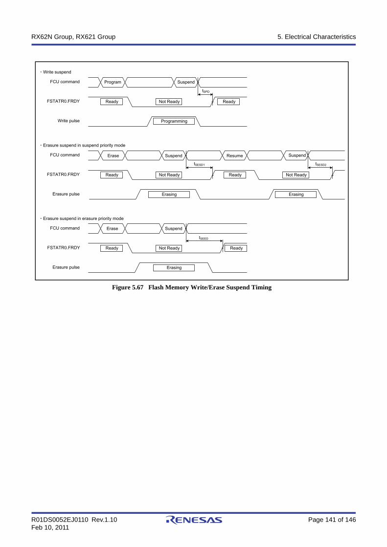
R01DS0052EJ0110 Rev.1.10 Page 141 of 146Feb 10, 2011
RX62N Group, RX621 Group 5. Electrical Characteristics
Figure 5.67 Flash Memory Write/Erase Suspend Timing
FCU command
FSTATR0.FRDY
Write pulse
・Write suspend
FCU command
FSTATR0.FRDY
Erasure pulse
・Erasure suspend in suspend priority mode
FCU command
FSTATR0.FRDY
Erasure pulse
・Erasure suspend in erasure priority mode
Program Suspend
Ready Not Ready Ready
Programming
tSPD
Erase Suspend
Ready Not Ready Ready
tSEED
Erasing
Erase Suspend Resume Suspend
Ready Not Ready Ready Not Ready
tSESD1 tSESD2
Erasing Erasing

R01DS0052EJ0110 Rev.1.10 Page 142 of 146Feb 10, 2011
RX62N Group, RX621 Group Appendix 1. Package Dimensions
Appendix 1.Package DimensionsInformation on the latest version of the package dimensions or mountings has been displayed in "Packages" on Renesas
Electronics Corp. website.
Figure A 176-Pin LFBGA (PLBG0176GA-A) Package Dimensions
e
A1
MaxNomMin
Dimension in Millimeters
SymbolReference
A
b
x
y
13.0
0.10
0.80
0.45 0.50 0.55
0.35 0.40 0.45
1.40
13.0
0.08
v
w
0.90
0.90
y1 0.2
0.20
0.15
ZE
ZD
SE
SD
E
D
1E
D
1
A
x4
A
B
φ x M S A B
S
Sy
Sw A Sw B
v
Sy1
2 3 4 5 6 7 8 9 10 11 12 13 14 15
B
C
D
E
F
G
H
J
K
L
M
N
P
R
φb
Z
e
e Z
A
A
E
D
Previous CodeJEITA Package Code RENESAS Code
BP-176/BP-176V 0.45g
MASS[Typ.]
P-LFBGA176-13x13-0.80 PLBG0176GA-A

R01DS0052EJ0110 Rev.1.10 Page 143 of 146Feb 10, 2011
RX62N Group, RX621 Group Appendix 1. Package Dimensions
Figure B 145-Pin TFLGA (PTLG0145JB-A) Package Dimensions
BASφ x n
B
A
Bw SAw S
S
y S
1y S
vx4
K
J
H
G
F
E
D
C
B
A
10987654321
D
E
L
11 12 13
M
N
Z
e
Z e
φb
AE
D
PTLG0145JB-AP-TFLGA145-9x9-0.65 0.15g
MASS[Typ.]Previous CodeJEITA Package Code RENESAS Code
-
e
A1
MaxNomMin
Dimension in Millimeters
SymbolReference
A
b
x
y
9.0
0.1
0.65
0.30 0.35 0.40
1.2
9.0
0.08
v
w
0.6
0.6
y1 0.20
0.20
0.15
ZE
ZD
SE
SD
E
D
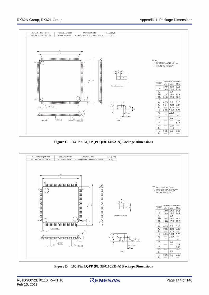
R01DS0052EJ0110 Rev.1.10 Page 144 of 146Feb 10, 2011
RX62N Group, RX621 Group Appendix 1. Package Dimensions
Figure C 144-Pin LQFP (PLQP0144KA-A) Package Dimensions
Figure D 100-Pin LQFP (PLQP0100KB-A) Package Dimensions
Terminal cross section
b1
c 1
bp
c
1.0
0.125
0.20
1.25
1.25
0.08
0.200.1450.09
0.270.220.17
MaxNomMin
Dimension in MillimetersSymbol
Reference
20.120.019.9D
20.120.019.9E
1.4A2
22.222.021.8
22.222.021.81.7A
0.150.10.05
0.650.50.35L
x
8°0°
c
0.5e
0.10y
HD
HE
A1
bp
b1
c1
ZD
ZE
L1
P-LQFP144-20x20-0.50 1.2g
MASS[Typ.]
144P6Q-A / FP-144L / FP-144LVPLQP0144KA-A
RENESAS CodeJEITA Package Code Previous Code
F
1 36
37
72
73108
109
144
*1
*2
*3
x
Index mark
y
HEE
D
HD
bp
ZD
ZE
Detail F
cA
LA1
A2
L1
2.
1. DIMENSIONS "*1" AND "*2"DO NOT INCLUDE MOLD FLASH.
NOTE)
DIMENSION "*3" DOES NOTINCLUDE TRIM OFFSET.
e
Terminal cross section
b1
c 1
bp
c
2.
1. DIMENSIONS "*1" AND "*2"DO NOT INCLUDE MOLD FLASH.
NOTE)
DIMENSION "*3" DOES NOTINCLUDE TRIM OFFSET.
y
Index mark
x
1 25
26
50
5175
76
100
F
*1
*3
*2
ZE
ZD
E
D
HD
HE
bp
Detail F
L1
A2
A1 L
A
c
L1
ZE
ZD
c1
b1
bp
A1
HE
HD
y 0.08
e 0.5
c
0° 8°
x
L 0.35 0.5 0.65
0.05 0.1 0.15
A 1.715.8 16.0 16.2
15.8 16.0 16.2
A2 1.4
E 13.9 14.0 14.1
D 13.9 14.0 14.1
ReferenceSymbol
Dimension in Millimeters
Min Nom Max
0.15 0.20 0.25
0.09 0.145 0.20
0.08
1.0
1.0
0.18
0.125
1.0
Previous CodeJEITA Package Code RENESAS Code
PLQP0100KB-A 100P6Q-A / FP-100U / FP-100UV
MASS[Typ.]
0.6gP-LQFP100-14x14-0.50
e

R01DS0052EJ0110 Rev.1.10 Page 145 of 146Feb 10, 2011
RX62N Group, RX621 Group Appendix 1. Package Dimensions
Figure E 85-Pin TFLGA (PTLG0085JA-A) Package Dimensions
B
A
Bw SAw S
S
y S
1y S
v
1 2 3 4 5 6 7 8 9 10
A
B
C
D
E
F
G
H
J
K
A
PTLG0085JA-AP-TFLGA85-7x7-0.65
D
E
D
E
SD
SE
ZD
ZE
Z D
Z E
MASS[Typ.]
0.1gTLP-85V
RENESAS CodeJEITA Package Code Previous Code
0.15
0.20
0.2y1
0.575
0.575
w
v
0.08
7.0
1.20
0.400.350.30
0.65
0.10
7.0
y
x
b
A
ReferenceSymbol
Dimension in Millimeters
Min Nom Max
A1
e
e
e
BASφ × bφ
M
×4

R01DS0052EJ0110 Rev.1.10 Page 146 of 146Feb 10, 2011
RX62N Group, RX621 Group REVISION HISTORY
REVISION HISTORY RX62N Group, RX621 Group Datasheet
Rev. DateDescription
Page Summary
1.00 2011.02.04 — First Edition issued
1.10 2011.02.10 — Features reviewed
All trademarks and registered trademarks are the property of their respective owners.
REVISION HISTORY