RTU-2-B-3 A 40GHz to 67GHz Bandwidth 23dB Gain 5.8dB ... · Bandwidth enhancement. RTU-2-B-3 •...
20
1 RFIC2015 RTU-2-B-3 A 40GHz to 67GHz Bandwidth 23dB Gain 5.8dB Maximum NF mm-Wave LNA in 28nm CMOS K. Hadipour 1,2 , A. Ghilioni 1 , A. Mazzanti 1 , M. Bassi 1 , F. Svelto 1 1 University of Pavia, Pavia, Italy 2 Johannes Kepler University, Linz, Austria RTU-2-B-3
Transcript of RTU-2-B-3 A 40GHz to 67GHz Bandwidth 23dB Gain 5.8dB ... · Bandwidth enhancement. RTU-2-B-3 •...

1
RFIC2015
RTU-2-B-3
A 40GHz to 67GHz Bandwidth 23dB Gain 5.8dB Maximum NF mm-Wave
LNA in 28nm CMOS
K. Hadipour1,2, A. Ghilioni1, A. Mazzanti1, M. Bassi1, F. Svelto1
1University of Pavia, Pavia, Italy2Johannes Kepler University, Linz, Austria
RTU-2-B-3

2
RFIC2015Outline
• Introduction• Bandwidth enhancement• High gain amplification• A high GBW amplifier• Proposed low noise amplifier• Measurement results• Conclusion
RTU-2-B-3
3
RFIC2015Introduction
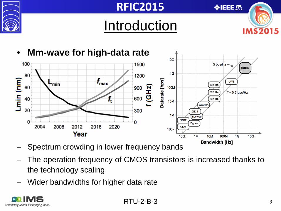
• Mm-wave for high-data rate
− Spectrum crowding in lower frequency bands− The operation frequency of CMOS transistors is increased thanks to
the technology scaling− Wider bandwidths for higher data rate
RTU-2-B-3
4
RFIC2015Introduction
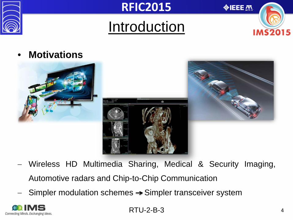
• Motivations
− Wireless HD Multimedia Sharing, Medical & Security Imaging,
Automotive radars and Chip-to-Chip Communication
− Simpler modulation schemes Simpler transceiver system
RTU-2-B-3
5
RFIC2015Bandwidth enhancement
RTU-2-B-3
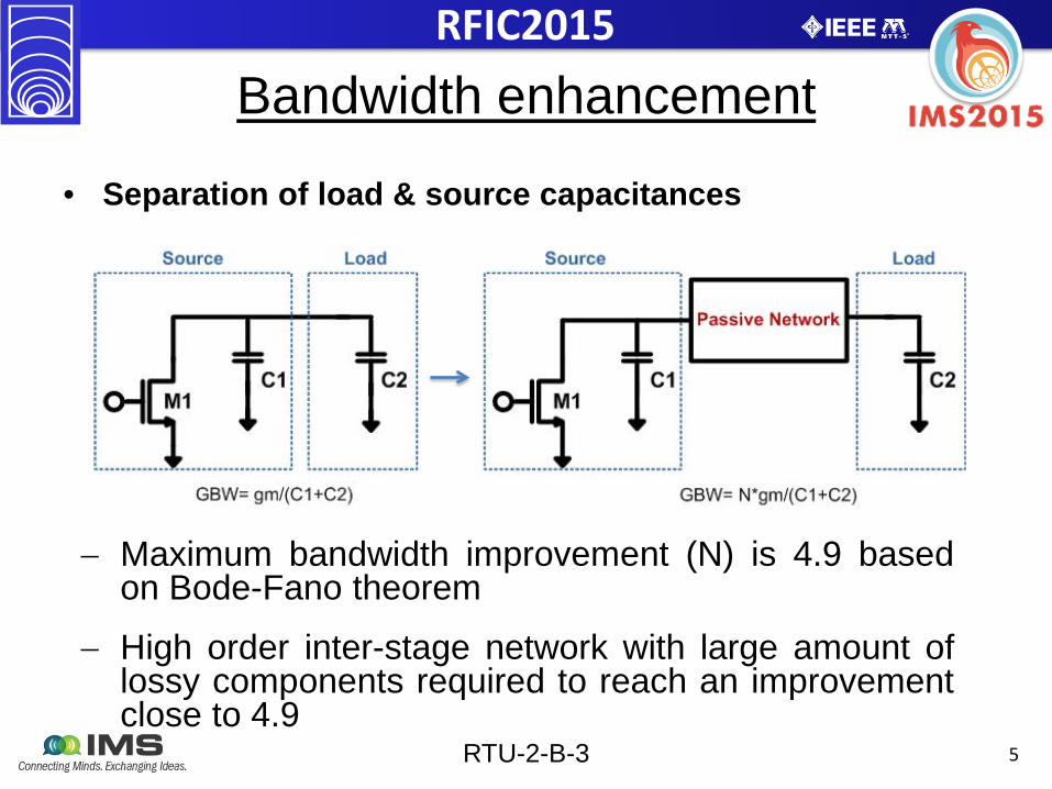
• Separation of load & source capacitances
− Maximum bandwidth improvement (N) is 4.9 basedon Bode-Fano theorem
− High order inter-stage network with large amount oflossy components required to reach an improvementclose to 4.9
6
RFIC2015Coupled resonators
RTU-2-B-3
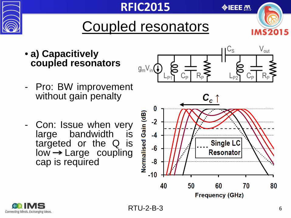
• a) Capacitivelycoupled resonators
- Pro: BW improvementwithout gain penalty
- Con: Issue when verylarge bandwidth istargeted or the Q islow Large couplingcap is required
7
RFIC2015Coupled resonators
RTU-2-B-3
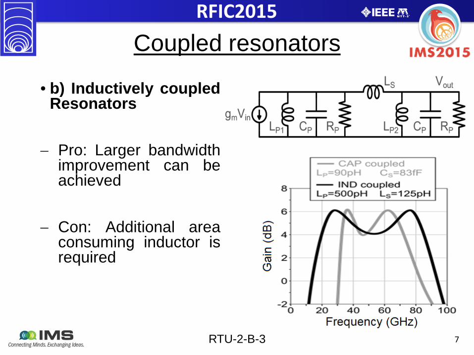
• b) Inductively coupledResonators
− Pro: Larger bandwidthimprovement can beachieved
− Con: Additional areaconsuming inductor isrequired
8
RFIC2015Proposed solution for inter-stage network
RTU-2-B-3
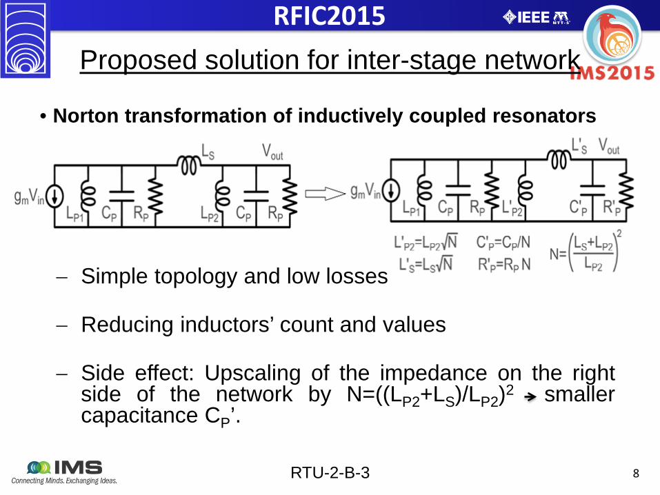
• Norton transformation of inductively coupled resonators
− Simple topology and low losses
− Reducing inductors’ count and values
− Side effect: Upscaling of the impedance on the rightside of the network by N=((LP2+LS)/LP2)2 smallercapacitance CP’.
9
RFIC2015Optimization of active stages
RTU-2-B-3
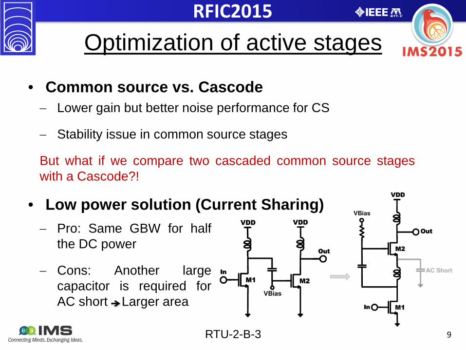
• Common source vs. Cascode
− Pro: Same GBW for halfthe DC power
− Cons: Another largecapacitor is required forAC short . Larger area
− Lower gain but better noise performance for CS
− Stability issue in common source stages
But what if we compare two cascaded common source stageswith a Cascode?!
• Low power solution (Current Sharing)
10
RFIC2015Proposed amplification stage
RTU-2-B-3
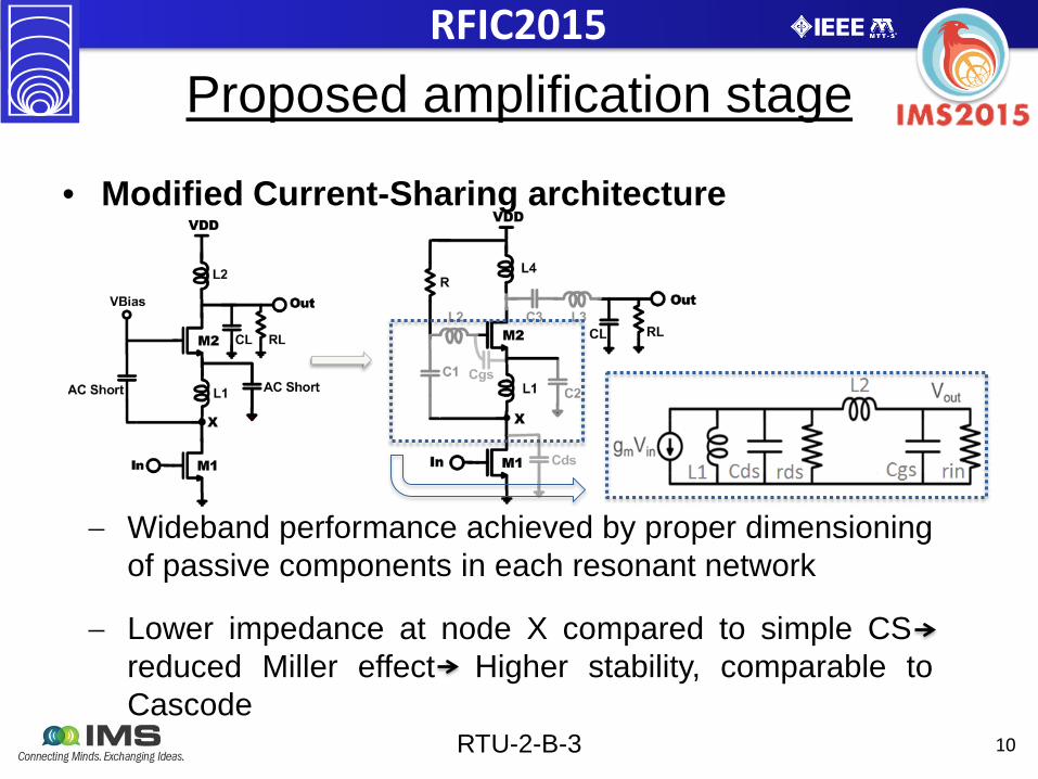
− Wideband performance achieved by proper dimensioningof passive components in each resonant network
− Lower impedance at node X compared to simple CS .
reduced Miller effect Higher stability, comparable toCascode
• Modified Current-Sharing architecture

11
RFIC2015Further bandwidth enhancement
RTU-2-B-3
− Wider BW for each network at the cost of more in-band ripple
− Stagger-tuning to compensate the in-band ripple andfurther extend BW
• Wideband stagger tuning
12
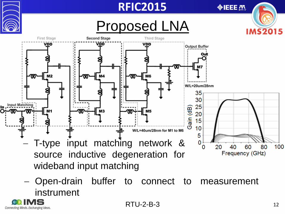
RFIC2015Proposed LNA
RTU-2-B-3
− Open-drain buffer to connect to measurementinstrument
− T-type input matching network &source inductive degeneration forwideband input matching
13
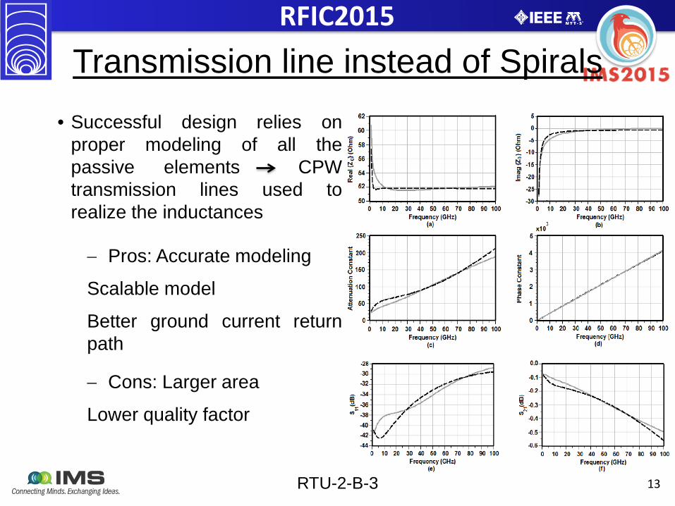
RFIC2015Transmission line instead of Spirals
RTU-2-B-3
• Successful design relies onproper modeling of all thepassive elements CPWtransmission lines used torealize the inductances
− Pros: Accurate modeling
Scalable model
Better ground current returnpath
− Cons: Larger area
Lower quality factor
14
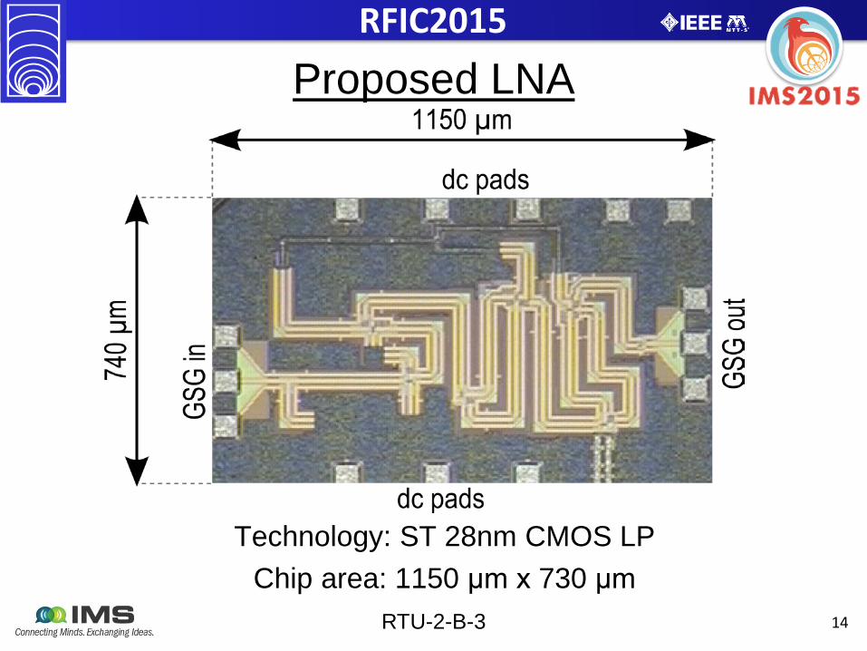
RFIC2015Proposed LNA
RTU-2-B-3
Technology: ST 28nm CMOS LPChip area: 1150 μm x 730 μm
15
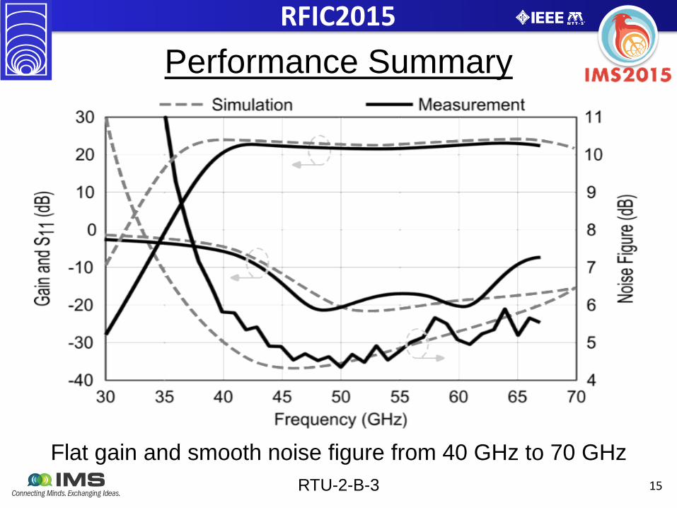
RFIC2015Performance Summary
Flat gain and smooth noise figure from 40 GHz to 70 GHzRTU-2-B-3

16
RFIC2015Performance Summary
K >10 and |∆|<1 in measured frequency bandOP-1dB > -4 dBm @ 60 GHz
RTU-2-B-3
17
RFIC2015Performance Summary
RTU-2-B-3
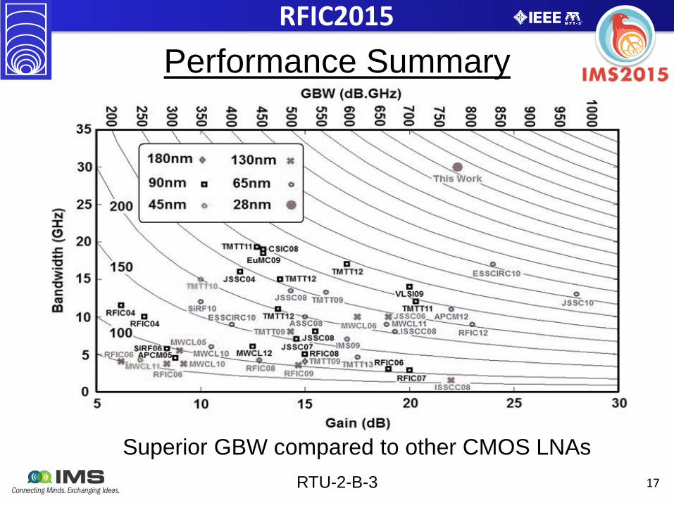
Superior GBW compared to other CMOS LNAs
18
RFIC2015Performance Summary
RTU-2-B-3
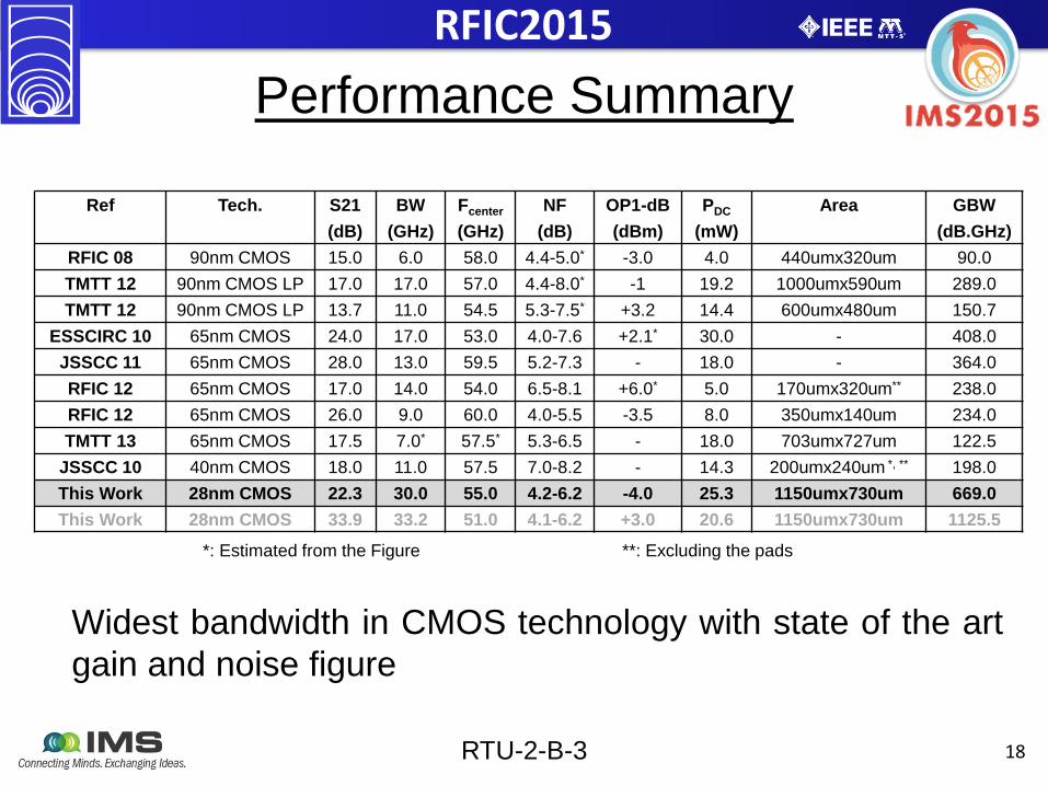
*: Estimated from the Figure **: Excluding the pads
Ref Tech. S21(dB)
BW(GHz)
Fcenter
(GHz)NF
(dB)OP1-dB (dBm)
PDC
(mW)Area GBW
(dB.GHz)RFIC 08 90nm CMOS 15.0 6.0 58.0 4.4-5.0* -3.0 4.0 440umx320um 90.0TMTT 12 90nm CMOS LP 17.0 17.0 57.0 4.4-8.0* -1 19.2 1000umx590um 289.0TMTT 12 90nm CMOS LP 13.7 11.0 54.5 5.3-7.5* +3.2 14.4 600umx480um 150.7
ESSCIRC 10 65nm CMOS 24.0 17.0 53.0 4.0-7.6 +2.1* 30.0 - 408.0JSSCC 11 65nm CMOS 28.0 13.0 59.5 5.2-7.3 - 18.0 - 364.0RFIC 12 65nm CMOS 17.0 14.0 54.0 6.5-8.1 +6.0* 5.0 170umx320um** 238.0RFIC 12 65nm CMOS 26.0 9.0 60.0 4.0-5.5 -3.5 8.0 350umx140um 234.0TMTT 13 65nm CMOS 17.5 7.0* 57.5* 5.3-6.5 - 18.0 703umx727um 122.5
JSSCC 10 40nm CMOS 18.0 11.0 57.5 7.0-8.2 - 14.3 200umx240um *, ** 198.0This Work 28nm CMOS 22.3 30.0 55.0 4.2-6.2 -4.0 25.3 1150umx730um 669.0This Work 28nm CMOS 33.9 33.2 51.0 4.1-6.2 +3.0 20.6 1150umx730um 1125.5
Widest bandwidth in CMOS technology with state of the artgain and noise figure
19
RFIC2015Conclusion
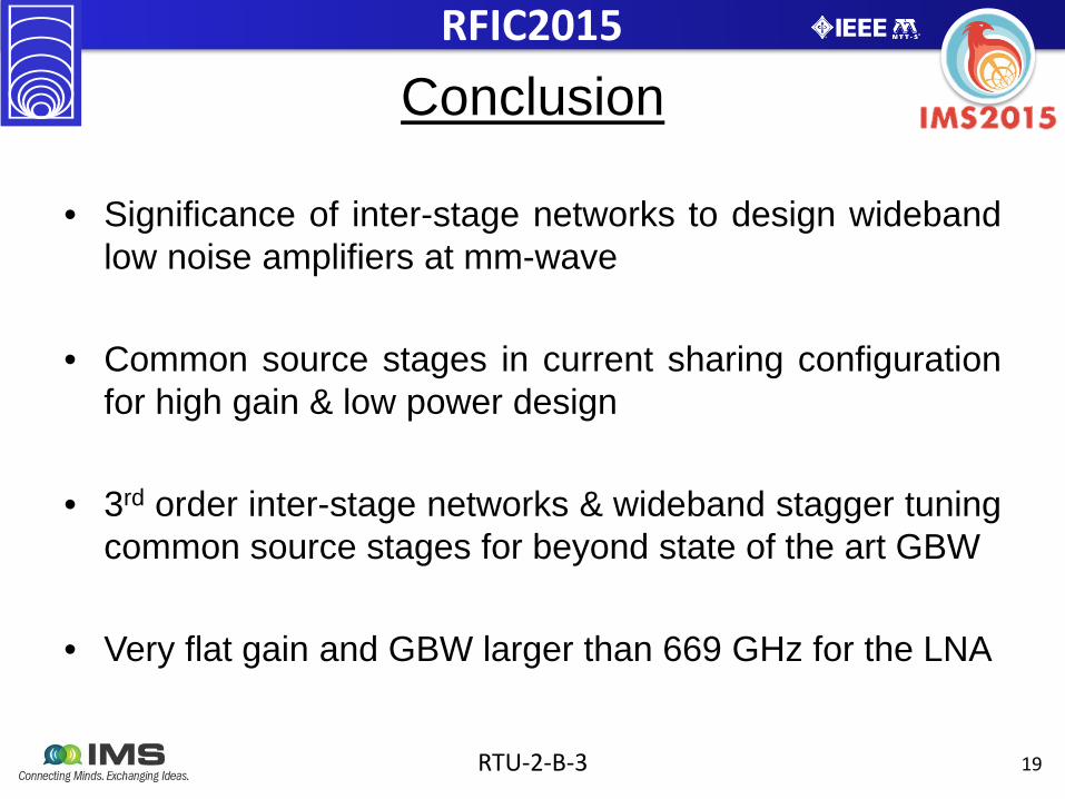
• Significance of inter-stage networks to design widebandlow noise amplifiers at mm-wave
• Common source stages in current sharing configurationfor high gain & low power design
• 3rd order inter-stage networks & wideband stagger tuningcommon source stages for beyond state of the art GBW
• Very flat gain and GBW larger than 669 GHz for the LNA
RTU-2-B-3
20
RFIC2015
Thank You!
RTU-2-B-3