Rockchip RK817 Datasheet
118
RK817 Datasheet Rev 1.01 Copyright ©2018 Fuzhou Rockchip Electronics Co., Ltd. 1 Rockchip RK817 Datasheet Revision 1.01 Aug.2018
Transcript of Rockchip RK817 Datasheet

RK817 Datasheet Rev 1.01
Copyright ©2018 Fuzhou Rockchip Electronics Co., Ltd. 1
Rockchip RK817
Datasheet
Revision 1.01 Aug.2018

RK817 Datasheet Rev 1.01
Copyright ©2018 Fuzhou Rockchip Electronics Co., Ltd. 2
Revision History
Date Revision Description
2018-8-28 1.01 Spec change @ power up sequence
2018-3-12 1.0 Initial release

RK817 Datasheet Rev 1.01
Copyright ©2018 Fuzhou Rockchip Electronics Co., Ltd. 3
Table of Content
Table of Content .................................................................................................. 3 Figure Index ....................................................................................................... 5 Table Index 6
Warranty Disclaimer ............................................................................................. 7 Chapter 1 Introduction ....................................................................................... 8
1.2 Feature ................................................................................................... 9
1.3 Typical Application Diagrams ..................................................................... 10
Chapter 2 Package information ........................................................................... 11
2.1 Ordering information ................................................................................ 11
2.2 Top Marking ............................................................................................ 11
2.3 Dimension .............................................................................................. 12
2.4 Pin Assignment ........................................................................................ 13
2.5 Pinout Number Order ............................................................................... 13
Chapter 3 Electrical Characteristics ...................................................................... 16
3.1 Absolute Maximum Ratings ....................................................................... 16
3.2 Recommended Operating Conditions ........................................................... 16
3.3 DC Characteristics ................................................................................... 16
Chapter 4 Function Description ........................................................................... 21
4.1 POWER UP/POWER DOWN ......................................................................... 21
4.2 SWITCHING CHARGER .............................................................................. 21
4.3 POWER PATH MANAGEMENT ...................................................................... 22
4.4 THERMAL FOLDBACK ................................................................................ 22
4.5 BATTERY FUEL GAUGE .............................................................................. 22
4.6 BUCK CONVERTERS ................................................................................. 22
4.7 BOOST CONVERTER ................................................................................. 23
4.8 LOW DROPOUT REGULATORS (LDOS) ......................................................... 23
4.9 REAL TIME CLOCK (RTC) ........................................................................... 23
4.10 RC OSCILLATOR ...................................................................................... 23
4.11 I2S interface ........................................................................................... 23
4.12 Audio CODEC .......................................................................................... 23
4.13 Head Phone driver ................................................................................... 23
4.14 ClassD driver .......................................................................................... 24
4.15 POWER SEQUENCE .................................................................................. 24
Chapter 5 Register Description ............................................................................ 25
5.1 Register Summary ................................................................................... 25

RK817 Datasheet Rev 1.01
Copyright ©2018 Fuzhou Rockchip Electronics Co., Ltd. 4
5.2 Register Description ................................................................................. 30
Chapter 6 Thermal Management ....................................................................... 118
6.1 Overview .............................................................................................. 118
6.2 Package Thermal Characteristics .............................................................. 118

RK817 Datasheet Rev 1.01
Copyright ©2018 Fuzhou Rockchip Electronics Co., Ltd. 5
Figure Index
Fig. 1-1RK817 Typical Application Diagram ......................................................... 10 Fig. 2-1QFN687mm X 7mm .............................................................................. 12 Fig. 2-2 Pin Assignment QFN7x7-68(Pitch=0.35mm) ........................................... 13

RK817 Datasheet Rev 1.01
Copyright ©2018 Fuzhou Rockchip Electronics Co., Ltd. 6
Table Index
Table 4-1Power up/down sequence(x:BUCK3 voltage determined by external divided resistor) .............................................................................................................. 24
Table 6-1 Thermal Resistance Characteristics .................................................... 118
RK817 Datasheet Rev 1.01
Copyright ©2018 Fuzhou Rockchip Electronics Co., Ltd. 7
Warranty Disclaimer Rockchip Electronics Co.,Ltd makes no warranty, representation or guarantee (expressed, implied, statutory, or otherwise) by or with respect to anything in this document, and shall not be liable for any implied warranties of non-infringement, merchantability or fitness for a particular purpose or for any indirect, special or consequential damages. Information furnished is believed to be accurate and reliable. However, Rockchip Electronics Co., Ltd assumes no responsibility for the consequences of use of such information or for any infringement of patents or other rights of third parties that may result from its use. Rockchip Electronics Co.,Ltd’s products are not designed, intended, or authorized for using as components in systems intended for surgical implant into the body, or other applications intended to support or sustain life, or for any other application in which the failure of the Rockchip Electronics Co.,Ltd’s product could create a situation where personal injury or death may occur, should buyer purchase or use Rockchip Electronics Co.,Ltd’s products for any such unintended or unauthorized application, buyers shall indemnify and hold Rockchip Electronics Co.,Ltd and its officers, employees, subsidiaries, affiliates, and distributors harmless against all claims, costs, damages, expenses, and reasonable attorney fees arising out of, either directly or indirectly, any claim of personal injury or death that may be associated with such unintended or unauthorized use, even if such claim alleges that Rockchip Electronics Co.,Ltd was negligent regarding the design or manufacture of the part.
Copyright and Patent Right Information in this document is provided solely to enable system and software implementers to use Rockchip Electronics Co., Ltd ’s products. There are no expressed or implied copyright licenses granted hereunder to design or fabricate any integrated circuits or integrated circuits based on the information in this document.
Rockchip Electronics Co.,Ltd does not convey any license under its patent rights nor the rights of others.
All copyright and patent rights referenced in this document belong to their respective owners and shall be subject to corresponding copyright and patent licensing requirements.
Trademarks Rockchip and RockchipTM logo and the name of Rockchip Electronics Co.,Ltd’s products are trademarks of Rockchip Electronics Co.,Ltd. and are exclusively owned by Rockchip Electronics Co.,Ltd. References to other companies and their products use trademarks owned by the respective companies and are for reference purpose only.
Confidentiality The information contained herein (including any attachments) is confidential. The recipient hereby acknowledges the confidentiality of this document, and except for the specific purpose, this document shall not be disclosed to any third party.
Reverse engineering or disassembly is prohibited. ROCKCHIP ELECTRONICS CO.,LTD. RESERVES THE RIGHT TO MAKE CHANGES IN ITS PRODUCTS OR PRODUCT SPECIFICATIONS WITH THE INTENT TO IMPROVE FUNCTION OR DESIGN AT ANY TIME AND WITHOUT NOTICE AND IS NOT REQUIRED TO UNDATE THIS DOCUMENTATION TO REFLECT SUCH CHANGES.
Copyright ©2018 Rockchip Electronics Co.,Ltd. All rights reserved. No part of this publication may be reproduced, stored in a retrieval system, or transmitted in any form or by any means, electric or mechanical, by photocopying, recording, or otherwise, without the prior written consent of Rockchip Electronics Co.,Ltd.

RK817 Datasheet Rev 1.01
Copyright ©2018 Fuzhou Rockchip Electronics Co., Ltd. 8
Chapter 1 Introduction
1.1 Overview
The RK817 is a complex power-management integrated circuit (PMIC) integrated
CODEC for multi-core system applications powered by a Li-ion or a Li-ion polymer battery
cell, or by a 5V input either from an USB port or from an adaptor. The RK817 can provide
a complete power management solution with very few external components.
The RK817 provides four configurable synchronous step-down converters. The
device also contains 9 LDO regulators, one switch-mode charger, a battery fuel gauge,
and the power path management function. Power-up/power-down controller is
configurable and can support any customized power-up/power-down sequences (OTP
based). A real-time clock (RTC) is also integrated to provide a 32.768-kHz output buffer,
and real time function. The RK817 supports 32.768-kHz clock generation based on a
crystal oscillator. It also includes Audio CODEC, real ground Head phone driver and
ClassD driver.
The switch-mode charger, together with the power path controller integrated in the
RK817, allows supplying power to the loads while it is charging the battery. The charger
provides functions such as input current limiting, trickle current charging, constant
current (CC)/constant voltage (CV) charging, charging termination, charging over time
protection, etc. All these functions can be conveniently configured through the I2C digital
interface. When an input current limiting is triggered, the power path controller will
distribute the input power in a way that the loads have the higher priority than the battery
to take the input power. The difference between the input and output power will be used
to charge the battery. In a case that the output power required by the loads exceeds the
input power, the power path controller will automatically turn on the battery switch so
that the battery can supply extra power to the loads together with the input supply. A
“battery fuel gauge” is also integrated in the RK817. Using the proprietary algorithms
and the sensed battery current and voltage, the gauge can accurately calculate the
battery capacity based on the charging/discharging characteristics of the battery
preloaded in the system. The gauge then sends the battery capacity information to the
processor through the I2C interface. Other functions that the charger provides includes
tiny current charging for an over discharged battery, or so called “dead battery”, battery
temperature monitoring, safe charging timer and over temperature shut down.
The RK817 can dynamically adjust the output voltage of each DC-DC converter, as
required by the processor based on the processor’s operation status so as to maximize
the system efficiency. The output voltages of most channels can be configured through
the I2C interface. The inputs of all channels have soft start function, which greatly
reduces the inrush current at the startup.
The 2MHz switching frequency allows small size inductors to be used for both buck
and boost converters. Also, as all the power switches are integrated on chip, no external
power switches and Schottky diodes are needed, which reduces the system cost
significantly.
The RK817 is available in a QFN68 7.0 mm x 7.0 mm package, with a 0.35-mm pin pitch.
RK817 Datasheet Rev 1.01
Copyright ©2018 Fuzhou Rockchip Electronics Co., Ltd. 9
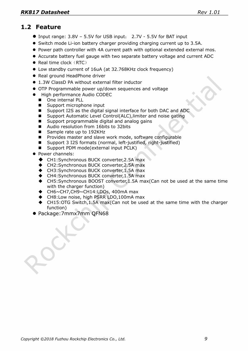
1.2 Feature
Input range: 3.8V – 5.5V for USB input; 2.7V - 5.5V for BAT input
Switch mode Li-ion battery charger providing charging current up to 3.5A.
Power path controller with 4A current path with optional extended external mos.
Accurate battery fuel gauge with two separate battery voltage and current ADC
Real time clock(RTC)
Low standby current of 16uA (at 32.768KHz clock frequency)
Real ground HeadPhone driver
1.3W ClassD PA without external filter inductor
OTP Programmable power up/down sequences and voltage
High performance Audio CODEC One internal PLL Support microphone input
Support I2S as the digital signal interface for both DAC and ADC Support Automatic Level Control(ALC),limiter and noise gating Support programmable digital and analog gains
Audio resolution from 16bits to 32bits Sample rate up to 192KHz Provides master and slave work mode, software configurable
Support 3 I2S formats (normal, left-justified, right-justified) Support PDM mode(external input PCLK)
Power channels:
CH1:Synchronous BUCK converter,2.5A max CH2:Synchronous BUCK converter,2.5A max CH3:Synchronous BUCK converter,1.5A max CH4:Synchronous BUCK converter,1.5A max
CH5:Synchronous BOOST converter,1.5A max(Can not be used at the same time with the charger function)
CH6~CH7,CH9~CH14:LDOs, 400mA max
CH8:Low noise, high PSRR LDO,100mA max CH15:OTG Switch,1.5A max(Can not be used at the same time with the charger
function)
Package:7mmx7mm QFN68

RK817 Datasheet Rev 1.01
Copyright ©2018 Fuzhou Rockchip Electronics Co., Ltd. 10
1.3 TypicalApplication Diagrams
XIN22pF
22pF
XOUT
32.768K
SW1
0.47uH/4A
33uF
VFB1
0.47uH/4A
33uF
VFB2
SW3
VFB3
SW4
VFB4
VCC110uF
Vsys
VCC210uF
Vsys
0.47uH/2.5A
22uF
10uF
Vsys
VCC3
VCC40.47uH/3A
22uF
10uF
VCC5
1uF
VLDO11uF
VLDO31uF
VLDO5
1uF
VCC61uF
VLDO4
1uF
VLDO61uF
CLK32K
VREF1uF
GNDREF
SLEEPSLEEP
INT
RESETB
PWRONPWRON
GATEGate
AP
(VCC_IO)
VCC_IO
RK817
SCL
4.7K
SDA
4.7K
SCL
SDA
100K 100K 100K
VCC_IO
VCC_IO
Exposed GND
BAT10uF
10 mohm
SNSP
SNSN
TS/GPIO
USB input /OTG output SYS Vsys
4.7uF
MIDU/BOOST22uF 0.47uH/5A 22uF*2
SW2
VLDO21uF
Vsys
Battery
pack
Vsy
s
Optional
SW5
SYSUSB/OTG
BAT
VLDO8
1uF
VCC71uF
VLDO7
1uF
VLDO91uF
VCC_IO
Vsys
MCLK
BCLK
LRCLKSDI
SDO/PDMDATA
MIC1P
MIC1N
HPR_OUTHPL_OUT
SPKP_OUT
VCC_SPK_HP10uF
Vsys
SPKN_OUT
CPP
CPN
VCC_CPVSS2.2uF
VCC_CPVDD1uF
HP_SNS
VCC_1P8A1uF
VCC_RTC1uF
Optional
2.2uF
VBUCK3
CODEC_IO
PDMCLK
VLDO
VCC_1P8D1uF
Vsys
Fig. 1-1RK817 Typical Application Diagram

RK817 Datasheet Rev 1.01
Copyright ©2018 Fuzhou Rockchip Electronics Co., Ltd. 11
Chapter 2 Package information
2.1 Ordering information
Orderable
Device
RoHS
status
Package Package Qty
RK817-1 RoHS QFN68(7X7) 2600ea/inner box* 6 inner
boxes/outer box
2.2 Top Marking
RK817-1
ABCXXXXXX DEFG
RockchipRKXXXX : Chip Name
Rockchip : Brand Name
ABC : Subcontractor CodeXXXXXX : Die Lot NO #DEFG : Date Code
The first pin

RK817 Datasheet Rev 1.01
Copyright ©2018 Fuzhou Rockchip Electronics Co., Ltd. 12
2.3 Dimension
Fig. 2-1QFN687mm X 7mm
DESCRIPTION SYMBOL MILLIMETER
MIN NOM MAX
TOTAL THICKNESS A 0.70 0.75 0.80
STAND OFF A1 0 0.035 0.05
MOLD THICKNESS A2 - 0.55 0.57
MATERIAL THICKNESS A3 - 0.203REF -
PACKAGE SIZE D - 7BSC -
E - 7BSC -
EP SIZE D1 5.39 5.49 5.59
E1 5.39 5.49 5.59
LEAD LENGTH L 0.30 0.4 0.50
LEAD PITCH e 0.35BSC
LEAD WIDTH b 0.1 0.15 0.2
LEAD OSITION OFFSET aaa 0.07
LEAD COPLANARITY bbb 0.08
PACKAGE EDGE PROFILE ccc 0.10
MOLD FLATNESS ddd 0.10
EP POSITION OFFSET eee 0.10
fff 0.05

RK817 Datasheet Rev 1.01
Copyright ©2018 Fuzhou Rockchip Electronics Co., Ltd. 13
Note:
1. Coplanarity applies to leads, corner leads and die attach pad.
2. Dimension b applies to metalized terminal and is measured between 0.15mm and 0.30mm from the
terminal tip. If the terminal has the optional radius on the other end of the terminal, the dimension
b should not be measure in that radius area.
2.4 Pin Assignment
VC
C5
LD
O2
LD
O1
LD
O3
SLEEP
INT
VC
C4
SW
4
FB
4
SW2
FB2
PW
RO
N
TS
/GP
IO
SN
SN
SN
SP
BA
T
SY
S
XOUT
MID
U/B
OO
ST
LD
O6
VREF
SDA
SCL
RE
SE
TB
VCC2
CL
K3
2K
GNDREF
VCC1
SW1
FB1
LD
O5
XIN
US
B/O
TG
LD
O4
VC
C6
FB
3
VC
C3
SW
3
1
2
3
4
5
6
7
8
10
11
12
13
14
15
9
16
17
18
19
20
21
22
23
24
25
27
28
29
30
31
32
26
33
34
51
50
49
48
47
46
45
44
42
41
40
39
38
37
43
36
35
68
67
66
65
64
63
62
61
59
58
57
56
55
54
60
53
52
QFN68 7×7ePAD
LDO9
LDO7
LDO8
MCLK
VCC7
BA
T
SY
S
SD
O/P
DM
DA
TA
LRCLK
SDI
BCLK
MIC1P
VCC_CPVSS
CPP
CPN
MIC1N
HPR_OUT
VCC_1P8A
VCC_CPVDD
HPL_OUT
VC
C_
SP
K_
HP
SP
KP
_O
UT
SP
KN
_O
UT
HP_SNS
VCC_RTC
VB
UC
K3
SW
5
PD
MC
LK
GA
TE
/GP
IO
VCC_1P8D
Fig. 2-2 Pin Assignment QFN7x7-68(Pitch=0.35mm)
2.5 Pinout Number Order
PIN NO PIN NAME PIN DESCRIPTION
1 SCL I2C clock input
2 SDA I2C data input and output(Open drain output)
3 LDO7 LDO7 output
4 VCC7 Power supply of LDO7/8/9
5 LDO8 LDO8 output
6 LDO9 LDO9 output
7 INT Interrupt request pin, open drain
8 FB2 Output feedback voltage of buck2
9 SW2 Switching node of buck2
10 VCC2 Power supply of buck2
11 VCC1 Power supply of buck1
12 SW1 Switching node of buck1
13 FB1 Output feedback voltage of buck1
14 LRCLK The I2S framing clock
15 BCLK The I2S bit clock
16 MCLK The I2S main clock input pin
17 SDI The I2S DAC input data
18 SDO/PDMDATA The I2S ADC output data/PDM Data for the DSADC
19 PDMCLK PDM CLK for the DSADC OUTPUT
20 LDO3 LDO3 output

RK817 Datasheet Rev 1.01
Copyright ©2018 Fuzhou Rockchip Electronics Co., Ltd. 14
PIN NO PIN NAME PIN DESCRIPTION
21 LDO2 LDO2 output
22 VCC5 Power supply of LDO1/2/3
23 LDO1 LDO1 output
24 VCC3 Power supply of buck3
25 SW3 Switching node of buck3
26 VBUCK3 Output voltage of buck3
27 FB3 Output feedback voltage of buck3
28 LDO4 LDO4 output, internal power supply for I2S
interface(Pin14~Pin19)
29 LDO5 LDO5 output
30 VCC6 Power supply of LDO4/5/6
31 LDO6 LDO6 output
32 SPKP_OUT Positive speaker driver output
33 VCC_SPK_HP Power supply for speaker and head phone
34 SPKN_OUT Negative speaker driver output.
35 VCC_CPVSS Negative power supply for the headphone
36 CPN Negative switching node of the charger pump
37 CPP Positive switching node of the charger pump.
38 VCC_CPVDD Positive power supply for the headphone
39 HPL_OUT Left channel output of the headphone
40 HP_SNS Reference ground for the headphone
41 HPR_OUT Right channel output of the headphone
42 MICIN Negative input of the Microphone
43 MICIP Positive input of the Microphone
44 VCC_1P8A Power supply for internal 1.8V analog circuit
45 VCC_RTC Power supply filter
46 VREF Internal reference voltage
47 GNDREF Reference ground
48 VCC_1P8D Power supply for internal 1.8V digital circuit
49 SLEEP Sleep mode control input
50 XIN 32.768KHz crystal oscillator input
51 XOUT 32.768KHz crystal oscillator output
52 PWRON Power on key input, active low, internal 17k resistor pull high to VCC_RTC
53 SW5 Switching node of charger/boost
54 MIDU/BOOST Middle point of USB power supply / boost output
55 USB/OTG USB power supply/OTG output
56,57 BAT Positive battery terminal
58,59 SYS DC-DC regulator output to power the system load and charge the battery
60 GATE/GPIO Control the external PMOS to reduce the conduction resistance or GPIO function by register setting
61 TS/GPIO Connect the thermistor from this pin to ground. Or it can be
used as an analog input pin of internal ADC if the control bit is set to ADC function or GPIO function by register setting
62 SNSP Bat charging and discharging sense current positive pin
63 SNSN Bat charging and discharging sense current negative pin
64 FB4 Output feedback voltage of buck4
65 SW4 Switching node of buck4
66 VCC4 Power supply of buck4

RK817 Datasheet Rev 1.01
Copyright ©2018 Fuzhou Rockchip Electronics Co., Ltd. 15
PIN NO PIN NAME PIN DESCRIPTION
67 RESETB Reset pin after power on, active low;
68 CLK32K 32.768KHz clock output, open drain
Exposed pad
Exposed ground
Ground

RK817 Datasheet Rev 1.01
Copyright ©2018 Fuzhou Rockchip Electronics Co., Ltd. 16
Chapter 3 Electrical Characteristics
3.1 Absolute Maximum Ratings
Parameter Min Max Units
Voltage range on pins USB/OTG, MIDU/BOOST, SWx, VCC1~7,VCC_RTC,VCC_SPK_HP,LDOx, SYS, BAT, FBx,VBUCK3,SPKP_OUT,SPKN_OUT
-0.3 6.5 V
Voltage range on pin CLK32K,RESETB, SLEEP,SCL,SDA,INT,PWRON,XIN,SOUT, TS/GPIO,GATE/GPIO,
-0.3 6.5 V
Voltage range on pins LRCLK,BCLK,MCLK,SDI,SDO/PDMCLK,PDMCLK,
-0.3 6.5 V
Voltage range on pins SNSP,SNSN,VREF,VCC_1P8D,VCC_1P8A,MIC1N,MIC1P
-0.2 1.98 V
Voltage range on pins HP_SNS,HPR_OUT,HPL_OUT -2.7 2.7 V
Voltage range on pins VCC_CPVDD,CPP -0.3 2.7 V
Voltage range on pins VCC_CPVSS,CPN -2.7 0.3 V
Storage temperature range, TS -40 150
Operating temperature range, TJ -40 125
Maximum Soldering Temperature, TSOLDER 300
Note:
Exposure to the conditions exceeded absolute maximum ratings may cause the permanent
damages and affect the reliability and safety of both device and systems using the device. The
functional operations cannot be guaranteed beyond specified values in the recommended
conditions.
3.2 Recommended Operating Conditions
Parameter Min TYP Max Units
Voltage range on pins USB/OTG 4 5 5.5 V
Power Dissipation 2 W
3.3 DC Characteristics
Test conditions: USB=5.0V,TA=25°C for typical values, unless otherwise noted.
PARAMETERS SYMBOL CONDITION MIN TYP MAX UNIT
USB INPUT
USB Operating Range VUSB 3.8 5 5.5 V
USB Input Current Limit IUSB
Default 400 450 500 mA
Max current 2.8 3 3.2 A
USB input VoltageLimit 0.1V step,
default=4.4V 4 4.7 V
CHARGER
Charge current ICC default=2A 0.5 3.5 A
A/D CONVERTER
Voltage measuring ADC resolution
12 bits

RK817 Datasheet Rev 1.01
Copyright ©2018 Fuzhou Rockchip Electronics Co., Ltd. 17
PARAMETERS SYMBOL CONDITION MIN TYP MAX UNIT
Range of USB/OTG voltage
measurement 1 6 V
Range of BAT voltage measurement
0 4.6 V
Range of SYS voltage measurement
1 6 V
Range of TS voltage measurement
0 1.2 V
Current measuring ADC resolution
15 bits
Range of Current ADC measurement
-56.25 56.25 mV
SYS INPUT
BAT to SYS Resistance ISYS=200mA ,
VBAT=4.2V 0.08 0.12 Ω
BAT to SYS Current Limit IBATLIM 0.5A step,default=3.5A
2 4 A
SYS short 200 mA
CH1:BUCK DC-DC CONVERTER(BUCK1)
Input supply voltage range VINPUT1 2.7 5.5 V
Voltage Adjustable Range, 7bit VFB1 Step=12.5mV(0.5V< VFB1<1.5)
Step=100mV(1.5V< VFB1<2.4)
0.5 2.4 V
Rated output current IMAX1 2.5 A
Conversion Efficiency(Vin=3.8V,Vout=1V)
Iout=2.5A
Iout=0.3A
70
85
%
CH2:BUCK DC-DC CONVERTER(BUCK2)
Input supply voltage range VINPUT2 2.7 5.5 V
Voltage Adjustable Range, 7bit VFB2 Step=12.5mV(0.5
V< VFB2<1.5) Step=100mV(1.5
V< VFB2<2.4)
0.5 2.4 V
Rated output current IMAX2 2.5 A
Conversion Efficiency(Vin=3.8V,Vout=1V)
Iout=2.5A
Iout=0.3A
70
85
%
CH3:BUCK DC-DC CONVERTER(BUCK3)
Input supply voltage range VINPUT3 2.7 5.5 V
Feedback Voltage, Default VFB3(Default) Selection of external resistor
divider
0.784 0.8 0.816 V
Voltage Adjustable Range, 7bit VFB3 Step=12.5mV(0.5V< VFB3<1.5)
Step=100mV(1.5V<VFB3<2.4) Selection of
internal resistor
divider
0.5 2.4 V
Rated output current IMAX3 1.5 A
Conversion Efficiency(Vin=3.8V,Vout=1.5V
) Iout=1.5A
Iout=0.3A
80
88
%

RK817 Datasheet Rev 1.01
Copyright ©2018 Fuzhou Rockchip Electronics Co., Ltd. 18
PARAMETERS SYMBOL CONDITION MIN TYP MAX UNIT
CH4:BUCK DC-DC CONVERTER(BUCK4)
Input supply voltage range VINPUT4 2.7 5.5 V
Voltage Adjustable Range, 7bit VFB4 Step=12.5mV(0.5
V< VFB4<1.5) Step=100mV(1.5
V< VFB4<3.4)
0.5 3.4 V
Rated output current IMAX4 1.5 A
Conversion Efficiency,
(Vin=3.8V,Vout=3.3V) Iout=1 .5A Iout=300mA
85
95
%
CH5:BOOST DC-DC CONVERTER (BOOST)
Input supply voltage range VINPUT5 2.7 4.4 V
Output Voltage VFB5 Step=0.1v,default=5v
4.7 5.4 V
Voltage, Default VFB5(Default) 4.90 5.0 5.10 V
Rated output current IMAX5 1.5 A
CH6:LDO1
Input supply voltage range VINPUT6 2 5.5 V
VOUT VOUT6 Step=25mV 0.6 3.4 V
Rated output current IMAX6 VINPUT6=3.6V, VOUT6=3.3V
RegLDO1_MAX=1
400 mA
VINPUT6=2V, VOUT6=1.8V
200 mA
CH7:LDO2
Input supply voltage range VINPUT7 2 5.5 V
VOUT VOUT7 Step=25mV 0.6 3.4 V
Rated output current IMAX7 VINPUT7=3.6V, VOUT7=3.3V
RegLDO2_MAX=1
400 mA
VINPUT7=2V, VOUT7=1.8V
200 mA
CH8:LDO3
Input supply voltage range VINPUT8 2 5.5 V
VOUT VOUT8 Step=25mV 0.6 3.4 V
Power Supply Reject Ratio (f = 10kHz, VOUT9=1.1V)
PSRR8 65 dB
Rated output current IMAX8 VINPUT8=3.6V, VOUT8=3.3V
RegLDO3_MAX=1
100 mA
VINPUT8=2V,
VOUT8=1.8V
100 mA
CH9: LDO4
Input supply voltage range VINPUT9 2 5.5 V
VOUT VOUT9 Step=25mV 0.6 3.4 V
Rated output current IMAX9 VINPUT9=3.6V, VOUT9=3.3V
RegLDO4_MAX=1
400 mA
VINPUT9=2V,
VOUT9=1.8V
200 mA
CH10:LDO5
Input supply voltage range VINPUT10 2 5.5 V
VOUT VOUT10 Step=25mV 0.6 3.4 V
Rated output current IMAX10 VINPUT10=3.6V,VOUT
10=3.3V RegLDO5_MAX=1
400 mA
VINPUT10=2V,
VOUT10=1.8V
200 mA
CH11:LDO6
Input supply voltage range VINPUT11 2 5.5 V

RK817 Datasheet Rev 1.01
Copyright ©2018 Fuzhou Rockchip Electronics Co., Ltd. 19
PARAMETERS SYMBOL CONDITION MIN TYP MAX UNIT VOUT VOUT11 Step=25mV 0.6 3.4 V
Rated output current IMAX11 VINPUT11=3.6V, VOUT11=3.3V
RegLDO6_MAX=1
400 mA
VINPUT11=2V, VOUT11=1.8V
200 mA
CH12:LDO7
Input supply voltage range VINPUT12 2 5.5 V
VOUT VOUT12 Step=25mV 0.6 3.4 V
Rated output current IMAX12 VINPUT12=3.6V, VOUT12=3.3V
RegLDO7_MAX=1
400 mA
VINPUT12=2V, VOUT12=1.8V
200 mA
CH13:LDO8
Input supply voltage range VINPUT13 2 5.5 V
VOUT VOUT13 Step=25mV 0.6 3.4 V
Rated output current IMAX13 VINPUT13=3.6V, VOUT13=3.3V
RegLDO8_MAX=1
400 mA
VINPUT13=2V, VOUT13=1.8V
200 mA
CH14:LDO9
Input supply voltage range VINPUT14 2 5.5 V
VOUT VOUT14 Step=25mV 0.6 3.4 V
Rated output current IMAX14 VINPUT14=3.6V, VOUT14=3.3V
RegLDO9_MAX=1
400 mA
VINPUT14=2V, VOUT14=1.8V
200 mA
CH15:OTG
Input supply voltage range VINPUT15 4.7 5.4 V
Rdson_OTG 90 mohm
Rated output current IMAX15 1500 mA
ClassD Audio PA
Input supply voltage range VINPUT14 VCC_SPK_HP 2.7 5.5 V
THD+N 1KHz, Po=0.4Wrms, VCC_SPK_HP
=3.8V
0.1 %
RMS Power 8 ohm load, VCC_SPK_HP
=3.8V, THD+N=1%
700 mW
8 ohm load,
VCC_SPK_HP
=5V, THD+N=1%
1100 mW
8 ohm load, VCC_SPK_HP
=5V, THD+N=10%
1300 mW
PSRR 217Hz, VCC_SPK_HP =200mVpk-
pk+3.8V,
65 dB
Output Offset Voltage VCC_SPK_HP
=3.8V
+/- 15 mV
Noise Level VCC_SPK_HP =3.8V 0dB Gain,
8ohm, A-weighted
100 uV
Efficiency VCC_SPK_HP
=3.8V,0.4W,8ohm with 68uH, 1KHz
88 %

RK817 Datasheet Rev 1.01
Copyright ©2018 Fuzhou Rockchip Electronics Co., Ltd. 20
PARAMETERS SYMBOL CONDITION MIN TYP MAX UNIT Quiescent current No load,
VCC_SPK_HP =3.8
4 mA
DAC to Head phone outputs
Full scale output level RL=32ohm 0.5 Vrms
RL=300ohm 0.8 Vrms
Signal to Noise Ratio SNR A-weighted RL=32ohm,-
60dBFS,
Fs=48KHz
97 dB
Total Harmonic Distortion + Noise
THD+N A-weighted RL=32ohm -
3dBFS Fs=48KHz
-75 dB
ADC stereo input
Full sale input voltage Vpp 1 V
SNR A-weighted,-
60dBFS,Fs=48KHz
88 dB
THD+N A-weighted 997Hz -3dBFS Differential input signal, Fs=48KHz
-75 dB
I2C interface (7bits I2C address is 0x20)
SCL clock frequency fSCL 1000 KHz
LOGIC INPUT
Input LOW-Level Voltage VIL 0.4 V
Input HIGH-Level Voltage: LRCLK,BCLK,MCLK,SDI,PDMCLK
VIH1 LDO4* 0.7
VCC_RTC
V
Input HIGH-Level Voltage:
SCL,SDA,SLEEP,PWRON,TS/GPIO,GATE/GPIO,RESETB
VIH2 VCC_1P
8D*0.7
VCC_RT
C
V
LOGIC OUTPUT
LOW-Level Output Voltage,
3.0 mA sink current
VOL 0.4 V
HIGH-Level Output Voltage,
3.0 mA source current:
LRCLK,BCLK,SDO/PDMDATA
VOH1 LDO4-
0.4
LDO4 V
HIGH-Level Output Voltage,
3.0 mA source current:
TS/GPIO,GATE/GPIO
VOH2 VCC_RT
C-0.4
VCC_RT
V
V
OPEN DRAIN OUTPUT PIN
CLK32K,RESETB,INT,SDA

RK817 Datasheet Rev 1.01
Copyright ©2018 Fuzhou Rockchip Electronics Co., Ltd. 21
Chapter 4 Function Description
4.1 POWER UP/POWER DOWN
The RK817 can be powered by either a battery, or an external power supply through the USB port. When the PMIC is powered by a battery only, pressing the PWRON key powers up the PMIC. All the power channels start up at the default output voltages with a preset power
up sequence, which has 2mS intervals between the channels. When the power up process is done, the RESETB turns to high logic level to inform the processor that all the power rails are up and stable. And now the processor can communicate with the PMIC to re-configure the
output voltage of each power channel if needed. To power down the PMIC, the processor needs to issue a “power down” signal through the
I2C interface. Upon receiving the power down signal, the PMIC first saves all the information on the existing states, and then switches the RESETB to low logic level. At this point, the
power channels start to be turned off one after another with the power down sequence. If for any reason the processor fails to issue the power down signal, the PMIC can be powered off by “pressing and holding” the PWRON key.
In a case where a battery is the sole power supply and the PMIC is in off state, when an
external power supply is plugged into the USB, the PMIC will first check to see if this is a valid
power supply. If the power supply from the USB is valid, then the power channels are turned on and the battery is charged.
4.2 SWITCHING CHARGER
The RK817 has integrated a switch mode charger, which provides the functions like trickle
current charging, constant current charging, constant voltage charging, charging termination, automatic recharging, battery temperature monitoring, charging timer and thermal feedback protection. The values of constant current and constant voltage charging can be set through
I2C interface. The input average current limit function allows as large as possible a charging current to
be used without having to worry about the input current exceeding the maximum current
allowed by the USB port. The input current limits can be configured through I2C interface. For example, when an USB port is used as the input, the input current limit can be configured to either 450mA, or 850mA, to meet the requirements of USB2.0 and USB3.0 respectively.
The charger also has a timer function which sets the maximum charging time for trickle,
constant current and constant voltage charging, respectively. If the charging does not
complete when a preset maximum charging time is reached, the charging is terminated. The battery temperature can be monitored through the TS pin. A battery typically has a
thermistor inside. The RK817 sinks a constant current into the thermistor and senses the voltage across the thermistor through an internal ADC. A safe charging temperature range is preset in the PMIC. The charging can proceed normally if the battery temperature falls within
the preset range. If, however, the battery temperature goes either above the upper limit or below the lower limit of the preset range, the charging will pause until the battery temperature goes back in the preset range. If the value of the available thermistor is either
too large or too small, a normal resistor can be connected in series or in parallel with the thermistor so that the sensed voltage fits the ADC’s input range.
During Charging, Vsyswill be set to 3.6V when the battery voltage is below 3.6V. This design is to guarantee that when an external power supply is plugged into the USB port to charge the battery while the battery voltage is low, the Vsys is already at 3.6V, which allows
the PMIC to start up quickly without having to wait for the Vsys ramping up.

RK817 Datasheet Rev 1.01
Copyright ©2018 Fuzhou Rockchip Electronics Co., Ltd. 22
4.3 POWER PATH MANAGEMENT
A power path management function is integrated in the RK817, which, together with the accurate input current limit function, can provide intelligent power path control. In a power path control process, the PMIC gives the outputs, or the system loads, the highest priority of
using the input power. The battery is getting charged only if the input power is greater than the output power required by the system loads. The intelligent power path control function automatically reduces the charging current when the output power required by the loads
increases. In an extreme case where the required output power is greater than the input power, the charging current will be cut off and the battery will join the input power supply to provide power to the load. This is how the intelligent power path control works: As the
system power loading increases, the PMIC will draw more input current from the power supply to meet the output power requirement while keep the charging current unchanged. If
the system power loading continues to increase to the point where the input current limit is reached, then the PMIC will lower the charging current so that enough power still goes to the load. If the system power loading further increases and due to the input current limit, the
input power can not meet the output power requirement, then the battery will start to discharge to supply power to the load together with the USB power supply. If for some reason the USB is unplugged, the battery will automatically switched in to take over the USB power
supply and provide full power to the load. The wide power path loop bandwidth allows all the above mentioned power path switching transient to be quick and seamless and therefore no overshoot and notch occur at the system and output voltages.
To minimize the loss from the voltage drop along the current path when the battery is
charged or discharged, a 100mΩ MOSFET is integrated in the RK817 to serve as a control
switch as well as the power switch of the switching mode battery charger.
4.4 THERMAL FOLDBACK
Generally speaking, the higher the operating junction temperature is, the shorter the
chip’s life time. Therefore, keeping the operating junction temperature as low as possible is one of the keys in reliability design. The RK817 provides a thermal feedback protection function for charging process. When the die temperature reaches a preset value, the PMIC
will lower the charging current so as to keep the die temperature within an appropriate range. The life time of the PMIC equipped with this function can be reliably prolonged and no over-heat damage will occur.
4.5 BATTERY FUEL GAUGE
The RK817 provides an accurate battery fuel gauge. A 12-bit battery voltage ADC and a 15-bit battery current ADC are integrated in the RK817 to collect the information on the
battery, such as battery voltage, charging/discharging status, battery temperature, etc. Using the proprietary algorithms and the information collected by the ADC, the battery fuel gauge can accurately calculate the battery capacity based on the charging/discharging
characteristics of the battery preloaded in the system. The gauge then sends the battery capacity information to the processor through the I2C interface.
4.6 BUCK CONVERTERS
The RK817 provides four high current synchronous buck converters, which deliver up to 2.5A, 2.5A, 1.5A and 1.5A, respectively. An enhanced COT architecture is used, which improves the transient response significantly. All output voltages can be adjusted dynamically
during operation through DVS (Dynamic Voltage Scaling), which guarantees a linear and gradual voltage ramping up and down. A complete set of protection functions, such as short circuit protection, is implemented in the buck converters too.

RK817 Datasheet Rev 1.01
Copyright ©2018 Fuzhou Rockchip Electronics Co., Ltd. 23
The key parameters such as operating mode, output voltage, DVS change rate, and output current limit can be configured through the I2C interface.
4.7 BOOST CONVERTER
The synchronous boost converter has 1.5A current capability and is used to power the
OTG. The OTG has a built-in current limiting switch, which can effectively protect the boost converter from being damaged if a short circuit occurs at the OTG port.
As the USB input port and the OTG output port share a same pin, when the USB port is being used as a power supply and charging the battery, the OTG switch is forbidden to be turned on. Only when there is no external power supply plugged into the USB port, can the
OTG be turned on and serve as a power supply.
The key parameters such as operating mode, output voltage, and output current limit can be configured through the I2C interface.
4.8 LOW DROPOUT REGULATORS (LDOS)
The RK817 also integrates nine LDOs, with 8 LDOs (Ch6, Ch7, Ch9 ~Ch14) capable of providing up to 400mA and one LDO (CH8 ) providing maximum 100mA. The LDO on CH8 is a low noise, high PSRR LDO . The parameters such as output voltage in the different
operating modes can be adjusted through the I2C interface.
4.9 REAL TIME CLOCK (RTC)
The RK817 integrates a crystal oscillator buffer and a real time clock (RTC). The buffer
works with an external 32.768kHz crystal oscillator. With the RTC function, the PMIC provides second/minute/hour/day/month/year information, alarm wake up as well as time calibration. The RK817 provides one channel of 32.768kHz clocks with open drain outputs, where it is
default on and is controlled through I2C interface.
4.10 RC OSCILLATOR
The RK817 integrates an RC oscillator. If the external crystal oscillator is not connected,
the chip will be driven by the internal RC oscillator. Without external crystal oscillator , the system costs can be saved, but the RTC and the fuel gauge will be inaccurate.
4.11 I2S interface
The RK817 supports I2S for the digital audio data interface. The I2S/PCM audio digital interface is used to input data to a stereo DAC or output data from a stereo ADC. The I2S/PCM audio interface can be configured to Master mode or Slave mode. In Master Mode,
BCLK and LRCLK are configured as output, but MCLK is fixed as input. In Slave Mode, BCLK and LRCLK are configured as input, and the MCLK is still as input.
4.12 Audio CODEC
The RK817 integrates a high performance stereo ADC and a high performance stereo DAC.
The audio recording path is composed of MIC_PGA and audio ADC.
4.13 Head Phone driver
The RK817 integrates a stereo output and with cap-free type headphone amplifier. It doesn’t need to connect external capacitance, and can connect to earphone device directly.

RK817 Datasheet Rev 1.01
Copyright ©2018 Fuzhou Rockchip Electronics Co., Ltd. 24
4.14 ClassD driver
The RK817 integrates a high efficiency stereo Class-D type amplifier capable of delivering 1.3W of power on an 8ohm BTL load from a 5V power supply. It integrates over-current protection.
4.15 POWER SEQUENCE
RK817-1
Range of output voltage
Maximum
output
current
Default
voltage
Start up
sequence
BUCK1 0.5V-2.4V 2.5A 1.1V 1
BUCK2 0.5V-2.4V 2.5A 1.1V 1
BUCK3
X(external divided resistor)
Or 0.5V-2.4v(internal divided
resistor)
1.5A x 3
BUCK4 0.5V-3.4V 1.5A 3.0V 4
BOOST 4.7V-5.4V 1.5A 5.0V OFF
LDO1 0.6V-3.4V 400mA 1.0V 2
LDO2 0.6V-3.4V 400mA 1.8V 2
LDO3 0.6V-3.4V 400mA 1.0V 1
LDO4 0.6V-3.4V 100mA 3.0V 4
LDO5 0.6V-3.4V 400mA 3.0V 4
LDO6 0.6V-3.4V 400mA 3.0V 4
LDO7 0.6V-3.4V 400mA 2.8V OFF
LDO8 0.6V-3.4V 400mA 1.8V OFF
LDO9 0.6V-3.4V 400mA 1.5V OFF
OTG Equals to BOOST 1.5A 5.0V OFF
Table 4-1Power up/down sequence(x:BUCK3 voltage determined by external divided resistor)

RK817 Datasheet Rev 1.01
Copyright ©2018 Fuzhou Rockchip Electronics Co., Ltd. 25
Chapter 5 Register Description
5.1 Register Summary
Name Offset Size Reset
Value Description
RTC_SECONDS 0x0000 B 0x00
RTC_MINUTES 0x0001 B 0x00
RTC_HOURS 0x0002 B 0x09
RTC_DAYS 0x0003 B 0x04
RTC_MONTHS 0x0004 B 0x08
RTC_YEARS 0x0005 B 0x17
RTC_WEEKS 0x0006 B 0x05
RTC_ALARM_SECONDS 0x0007 B 0x00
RTC_ALARM_MINUTES 0x0008 B 0x00
RTC_ALARM_HOURS 0x0009 B 0x00
RTC_ALARM_DAYS 0x000a B 0x01
RTC_ALARM_MONTHS 0x000b B 0x01
RTC_ALARM_YEARS 0x000c B 0x00
RTC_RTC_CTRL 0x000d B 0x00
RTC_RTC_STATUS 0x000e B 0x82
RTC_RTC_INT 0x000f B 0x00
RTC_RTC_COMP_LSB 0x0010 B 0x00
RTC_RTC_COMP_MSB 0x0011 B 0x00
CODEC_DTOP_VUCTL 0x0012 B 0x03
CODEC_DTOP_VUCTIME 0x0013 B 0x00
CODEC_DTOP_LPT_SRST 0x0014 B 0x00
CODEC_DTOP_DIGEN_CLKE 0x0015 B 0x00
CODEC_AREF_RTCFG1 0x0017 B 0x06
CODEC_AADC_CFG0 0x0018 B 0xc8
CODEC_DADC_VOLL 0x001a B 0x00
CODEC_DADC_VOLR 0x001b B 0x00
CODEC_DADC_SR_ACL0 0x001e B 0x00
CODEC_DADC_ALC1 0x001f B 0x00
CODEC_DADC_ALC2 0x0020 B 0x00
CODEC_DADC_NG 0x0021 B 0x00
CODEC_DADC_HPF 0x0022 B 0x00
CODEC_DADC_RVOLL 0x0023 B 0xff
CODEC_DADC_RVOLR 0x0024 B 0xff
CODEC_AMIC_CFG0 0x0027 B 0x70
CODEC_AMIC_CFG1 0x0028 B 0x00
CODEC_DMIC_PGA_GAIN 0x0029 B 0x66
CODEC_DMIC_LMT1 0x002a B 0x00
CODEC_DMIC_LMT2 0x002b B 0x00
CODEC_DMIC_NG1 0x002c B 0x00

RK817 Datasheet Rev 1.01
Copyright ©2018 Fuzhou Rockchip Electronics Co., Ltd. 26
Name Offset Size Reset
Value Description
CODEC_DMIC_NG2 0x002d B 0x00
CODEC_ADAC_CFG1 0x002f B 0x07
CODEC_DDAC_POPD_DACST 0x0030 B 0x82
CODEC_DDAC_VOLL 0x0031 B 0x00
CODEC_DDAC_VOLR 0x0032 B 0x00
CODEC_DDAC_SR_LMT0 0x0035 B 0x00
CODEC_DDAC_LMT1 0x0036 B 0x00
CODEC_DDAC_LMT2 0x0037 B 0x00
CODEC_DDAC_MUTE_MIXCTL 0x0038 B 0xa0
CODEC_DDAC_RVOLL 0x0039 B 0xff
CODEC_DDAC_RVOLR 0x003a B 0xff
CODEC_AHP_ANTI0 0x003b B 0x00
CODEC_AHP_ANTI1 0x003c B 0x00
CODEC_AHP_CFG0 0x003d B 0xe0
CODEC_AHP_CFG1 0x003e B 0x1f
CODEC_AHP_CP 0x003f B 0x09
CODEC_ACLASSD_CFG1 0x0040 B 0x69
CODEC_ACLASSD_CFG2 0x0041 B 0x44
CODEC_APLL_CFG0 0x0042 B 0x04
CODEC_APLL_CFG1 0x0043 B 0x00
CODEC_APLL_CFG2 0x0044 B 0x30
CODEC_APLL_CFG3 0x0045 B 0x19
CODEC_APLL_CFG4 0x0046 B 0x65
CODEC_APLL_CFG5 0x0047 B 0x01
CODEC_DI2S_CKM 0x0048 B 0x01
CODEC_DI2S_RSD 0x0049 B 0x00
CODEC_DI2S_RXCR1 0x004a B 0x00
CODEC_DI2S_RXCR2 0x004b B 0x17
CODEC_DI2S_RXCMD_TSD 0x004c B 0x00
CODEC_DI2S_TXCR1 0x004d B 0x00
CODEC_DI2S_TXCR2 0x004e B 0x17
CODEC_DI2S_TXCR3_TXCMD 0x004f B 0x00
gas_gauge_ADC_CONFIG0 0x0050 B 0x8c
gas_gauge_ADC_CONFIG1 0x0055 B 0x30
gas_gauge_GG_CON 0x0056 B 0x44
gas_gauge_GG_STS 0x0057 B 0x00
gas_gauge_RELAX_THRE_H 0x0058 B 0x00
gas_gauge_RELAX_THRE_L 0x0059 B 0x60
gas_gauge_RELAX_VOL1_H 0x005a B 0x00
gas_gauge_RELAX_VOL1_L 0x005b B 0x00
gas_gauge_RELAX_VOL2_H 0x005c B 0x00
gas_gauge_RELAX_VOL2_L 0x005d B 0x00
gas_gauge_RELAX_CUR1_H 0x005e B 0x00

RK817 Datasheet Rev 1.01
Copyright ©2018 Fuzhou Rockchip Electronics Co., Ltd. 27
Name Offset Size Reset
Value Description
gas_gauge_RELAX_CUR1_L 0x005f B 0x00
gas_gauge_RELAX_CUR2_H 0x0060 B 0x00
gas_gauge_RELAX_CUR2_L 0x0061 B 0x00
gas_gauge_OCV_THRE_VOL 0x0062 B 0x00
gas_gauge_OCV_VOL_H 0x0063 B 0x00
gas_gauge_OCV_VOL_L 0x0064 B 0x00
gas_gauge_OCV_VOL0_H 0x0065 B 0x00
gas_gauge_OCV_VOL0_L 0x0066 B 0x00
gas_gauge_OCV_CUR_H 0x0067 B 0x00
gas_gauge_OCV_CUR_L 0x0068 B 0x00
gas_gauge_OCV_CUR0_H 0x0069 B 0x00
gas_gauge_OCV_CUR0_L 0x006a B 0x00
gas_gauge_PWRON_VOL_H 0x006b B 0x00
gas_gauge_PWRON_VOL_L 0x006c B 0x00
gas_gauge_PWRON_CUR_H 0x006d B 0x00
gas_gauge_PWRON_CUR_L 0x006e B 0x00
gas_gauge_OFF_CNT 0x006f B 0x00
gas_gauge_Q_INIT_H3 0x0070 B 0x00
gas_gauge_Q_INIT_H2 0x0071 B 0x00
gas_gauge_Q_INIT_L1 0x0072 B 0x00
gas_gauge_Q_INIT_L0 0x0073 B 0x00
gas_gauge_Q_PRES_H3 0x0074 B 0x00
gas_gauge_Q_PRES_H2 0x0075 B 0x00
gas_gauge_Q_PRES_L1 0x0076 B 0x00
gas_gauge_Q_PRES_L0 0x0077 B 0x00
gas_gauge_BAT_VOL_H 0x0078 B 0x00
gas_gauge_BAT_VOL_L 0x0079 B 0x00
gas_gauge_BAT_CUR_H 0x007a B 0x00
gas_gauge_BAT_CUR 0x007b B 0x00
gas_gauge_BAT_TS_H 0x007c B 0x00
gas_gauge_BAT_TS_L 0x007d B 0x00
gas_gauge_USB_VOL_H 0x007e B 0x00
gas_gauge_USB_VOL_L 0x007f B 0x00
gas_gauge_SYS_VOL_H 0x0080 B 0x00
gas_gauge_SYS_VOL_L 0x0081 B 0x00
gas_gauge_Q_MAX_H3 0x0082 B 0x00
gas_gauge_Q_MAX_H2 0x0083 B 0x00
gas_gauge_Q_MAX_L1 0x0084 B 0x00
gas_gauge_Q_MAX_L0 0x0085 B 0x00
gas_gauge_Q_TERM_H3 0x0086 B 0x00
gas_gauge_Q_TERM_H2 0x0087 B 0x00
gas_gauge_Q_TERM_L1 0x0088 B 0x00
gas_gauge_Q_TERM_L0 0x0089 B 0x00

RK817 Datasheet Rev 1.01
Copyright ©2018 Fuzhou Rockchip Electronics Co., Ltd. 28
Name Offset Size Reset
Value Description
gas_gauge_Q_OCV_H3 0x008a B 0x00
gas_gauge_Q_OCV_H2 0x008b B 0x00
gas_gauge_Q_OCV_L1 0x008c B 0x00
gas_gauge_Q_OCV_L0 0x008d B 0x00
gas_gauge_OCV_CNT 0x008e B 0x00
gas_gauge_SLEEP_CON_SAMP
_CUR_H 0x008f B 0x00
gas_gauge_SLEEP_CON_SAMP
_CUR 0x0090 B 0x60
gas_gauge_CAL_OFFSET_H 0x0091 B 0x7f
gas_gauge_CAL_OFFSET_L 0x0092 B 0xff
gas_gauge_VCALIB0_H 0x0093 B 0x00
gas_gauge_VCALIB0_L 0x0094 B 0x00
gas_gauge_VCALIB1_H 0x0095 B 0x00
gas_gauge_VCALIB1_L 0x0096 B 0x00
gas_gauge_IOFFSET_H 0x0097 B 0x00
gas_gauge_IOFFSET_L 0x0098 B 0x00
gas_gauge_BAT_R0 0x0099 B 0x00
gas_gauge_BAT_R1 0x009a B 0x00
gas_gauge_BAT_R2 0x009b B 0x00
gas_gauge_BAT_R3 0x009c B 0x00
gas_gauge_DATA0 0x009d B 0x00
gas_gauge_DATA1 0x009e B 0x00
gas_gauge_DATA2 0x009f B 0x00
gas_gauge_DATA3 0x00a0 B 0x00
gas_gauge_DATA4 0x00a1 B 0x00
gas_gauge_DATA5 0x00a2 B 0x00
gas_gauge_DATA6 0x00a3 B 0x00
gas_gauge_DATA7 0x00a4 B 0x00
gas_gauge_DATA8 0x00a5 B 0x00
gas_gauge_DATA9 0x00a6 B 0x00
gas_gauge_DATA10 0x00a7 B 0x00
gas_gauge_DATA11 0x00a8 B 0x00
gas_gauge_VOL_ADC_B3 0x00a9 B 0x00
gas_gauge_VOL_ADC_B2 0x00aa B 0x00
gas_gauge_VOL_ADC_B1 0x00ab B 0x00
gas_gauge_VOL_ADC_B_7_0 0x00ac B 0x00
gas_gauge_CUR_ADC_K3 0x00ad B 0x00
gas_gauge_CUR_ADC_K2 0x00ae B 0x00
gas_gauge_CUR_ADC_K1 0x00af B 0x00
gas_gauge_CUR_ADC_K0 0x00b0 B 0x00
PMIC_POWER_EN0 0x00b1 B 0x0f
PMIC_POWER_EN1 0x00b2 B 0x0f

RK817 Datasheet Rev 1.01
Copyright ©2018 Fuzhou Rockchip Electronics Co., Ltd. 29
Name Offset Size Reset
Value Description
PMIC_POWER_EN2 0x00b3 B 0x06
PMIC_POWER_EN3 0x00b4 B 0x00
PMIC_POWER_SLP_EN0 0x00b5 B 0x0f
PMIC_POWER_SLP_EN1 0x00b6 B 0x6f
PMIC_POWER_DISCHRG_EN0 0x00b7 B 0xff
PMIC_POWER_DISCHRG_EN1 0x00b8 B 0xff
PMIC_POWER_CONFIG 0x00b9 B 0x00
PMIC_BUCK1_CONFIG 0x00ba B 0x64
PMIC_BUCK1_ON_VSEL 0x00bb B 0x28
PMIC_BUCK1_SLP_VSEL 0x00bc B 0x28
PMIC_BUCK2_CONFIG 0x00bd B 0x64
PMIC_BUCK2_ON_VSEL 0x00be B 0x28
PMIC_BUCK2_SLP_VSEL 0x00bf B 0x28
PMIC_BUCK3_CONFIG 0x00c0 B 0x64
PMIC_BUCK3_ON_VSEL 0x00c1 B 0x50
PMIC_BUCK3_SLP_VSEL 0x00c2 B 0x50
PMIC_BUCK4_CONFIG 0x00c3 B 0x64
PMIC_BUCK4_ON_VSEL 0x00c4 B 0x62
PMIC_BUCK4_SLP_VSEL 0x00c5 B 0x62
PMIC_BUCK4_CMIN 0x00c6 B 0x04
PMIC_LDO1_ON_VSEL 0x00cc B 0x6c
PMIC_LDO1_SLP_VSEL 0x00cd B 0x6c
PMIC_LDO2_ON_VSEL 0x00ce B 0x10
PMIC_LDO2_SLP_VSEL 0x00cf B 0x10
PMIC_LDO3_ON_VSEL 0x00d0 B 0x6c
PMIC_LDO3_SLP_VSEL 0x00d1 B 0x6c
PMIC_LDO4_ON_VSEL 0x00d2 B 0x10
PMIC_LDO4_SLP_VSEL 0x00d3 B 0x10
PMIC_LDO5_ON_VSEL 0x00d4 B 0x30
PMIC_LDO5_SLP_VSEL 0x00d5 B 0x30
PMIC_LDO6_ON_VSEL 0x00d6 B 0x30
PMIC_LDO6_SLP_VSEL 0x00d7 B 0x30
PMIC_LDO7_ON_VSEL 0x00d8 B 0x30
PMIC_LDO7_SLP_VSEL 0x00d9 B 0x30
PMIC_LDO8_ON_VSEL 0x00da B 0x6c
PMIC_LDO8_SLP_VSEL 0x00db B 0x6c
PMIC_LDO9_ON_VSEL 0x00dc B 0x58
PMIC_LDO9_SLP_VSEL 0x00dd B 0x58
PMIC_BOOST_OTG_CONFIG0 0x00de B 0x0b
PMIC_BOOST_CONFIG1 0x00df B 0x33
PMIC_CHRG_OUT 0x00e4 B 0xa2
PMIC_CHRG_IN 0x00e5 B 0xc8
PMIC_CHRG_TERM 0x00e6 B 0xc1

RK817 Datasheet Rev 1.01
Copyright ©2018 Fuzhou Rockchip Electronics Co., Ltd. 30
Name Offset Size Reset
Value Description
PMIC_CHRG_TERM_DIG 0x00e7 B 0x00
PMIC_BAT_HTS_TS 0x00e8 B 0x00
PMIC_BAT_LTS_TS 0x00e9 B 0xff
PMIC_CHRG_TO 0x00ea B 0x22
PMIC_CHRG_STS 0x00eb B 0x00
PMIC_BAT_DISCHRG 0x00ec B 0x0a
PMIC_CHIP_NAME 0x00ed B 0x81
PMIC_CHIP_VER 0x00ee B 0x72
PMIC_OTP_VER 0x00ef B 0x00
PMIC_SYS_STS 0x00f0 B 0x00
PMIC_SYS_CFG0 0x00f1 B 0x84
PMIC_SYS_CFG1 0x00f2 B 0x80
PMIC_SYS_CFG2 0x00f3 B 0x00
PMIC_SYS_CFG3 0x00f4 B 0x20
PMIC_ON_SOURCE 0x00f5 B 0x00
PMIC_OFF_SOURCE 0x00f6 B 0x00
PMIC_PWRON_KEY 0x00f7 B 0x06
PMIC_INT_STS0 0x00f8 B 0x00
PMIC_INT_MSK0 0x00f9 B 0x00
PMIC_INT_STS1 0x00fa B 0x00
PMIC_INT_MSK1 0x00fb B 0x00
PMIC_INT_STS2 0x00fc B 0x00
PMIC_INT_MSK2 0x00fd B 0x00
PMIC_GPIO_INT_CONFIG 0x00fe B 0x22
Notes:Size:B- Byte (8 bits) access, HW- Half WORD (16 bits) access, W-WORD (32 bits) access
5.2 Register Description
RTC_SECONDS Address: Operational Base + offset (0x0000)
Bit Attr Reset Value Description
7 RW 0x0 RESV
Reserved
6:4 RW 0x0
SEC1
Set the second digit of the RTC seconds (0-
5)
3:0 RW 0x0 SEC0
Set the first digit of the RTC seconds (0-9)
RTC_MINUTES Address: Operational Base + offset (0x0001)

RK817 Datasheet Rev 1.01
Copyright ©2018 Fuzhou Rockchip Electronics Co., Ltd. 31
Bit Attr Reset Value Description
7 RW 0x0 RESV
Reserved
6:4 RW 0x0
MIN1
Set the second digit of the RTC minutes (0-
5)
3:0 RW 0x0 MIN0
Set the first digit of the RTC minutes (0-9)
RTC_HOURS Address: Operational Base + offset (0x0002)
Bit Attr Reset Value Description
7 RW 0x0 AMPM
Only used in PM-AM mode, 1: PM. 0:AM
6 RW 0x0 RESV
Reserved
5:4 RW 0x0 HOUR1
Set the second digit of the RTC hours
3:0 RW 0x9 HOUR0
Set the first digit of the RTC hours
RTC_DAYS
Address: Operational Base + offset (0x0003)
Bit Attr Reset Value Description
7:6 RW 0x0 RESV
Reserved
5:4 RW 0x0 DAY1
Set the second digit of the RTC days
3:0 RW 0x4 DAY0
Set the first digit of the RTC days
RTC_MONTHS
Address: Operational Base + offset (0x0004)
Bit Attr Reset Value Description
7:5 RW 0x0 RESV
Reserved
4 RW 0x0 MONTH1
Set the second digit of the RTC months
3:0 RW 0x8 MONTH0
Set the first digit of the RTC months
RTC_YEARS

RK817 Datasheet Rev 1.01
Copyright ©2018 Fuzhou Rockchip Electronics Co., Ltd. 32
Address: Operational Base + offset (0x0005)
Bit Attr Reset Value Description
7:4 RW 0x1 YEAR1
Set the second digit of the RTC years
3:0 RW 0x7 YEAR0
Set the first digit of the RTC years
RTC_WEEKS Address: Operational Base + offset (0x0006)
Bit Attr Reset Value Description
7:3 RW 0x00 RESV
Reserved
2:0 RW 0x5 WEEK
Set the second digit of the RTC weeks
RTC_ALARM_SECONDS Address: Operational Base + offset (0x0007)
Bit Attr Reset Value Description
7 RW 0x0 RESV
Reserved
6:4 RW 0x0
ALARM_SEC1
Set the second digit of the RTC alarm
seconds
3:0 RW 0x0 ALARM_SEC0
Set the first digit of the RTC alarm seconds
RTC_ALARM_MINUTES Address: Operational Base + offset (0x0008)
Bit Attr Reset Value Description
7 RW 0x0 RESV
Reserved
6:4 RW 0x0
ALARM_MIN1
Set the second digit of the RTC alarm
minutes
3:0 RW 0x0 ALARM_MIN0
Set the first digit of the RTC alarm minutes
RTC_ALARM_HOURS Address: Operational Base + offset (0x0009)
RK817 Datasheet Rev 1.01
Copyright ©2018 Fuzhou Rockchip Electronics Co., Ltd. 33
Bit Attr Reset Value Description
7 RW 0x0
ALARM_PM_AM
Set alarm PM or AM: only used in PM-AM
mode, 1: PM. 0:AM
6 RW 0x0 RESV
Reserved
5:4 RW 0x0 ALARM_HOUR1
Set the second digit of the RTC alarm hours
3:0 RW 0x0 ALARM_HOUR0
Set the first digit of the RTC alarm hours
RTC_ALARM_DAYS Address: Operational Base + offset (0x000a)
Bit Attr Reset Value Description
7:6 RW 0x0 RESV
Reserved
5:4 RW 0x0 ALARM_DAY1
Set the second digit of the RTC alarm days
3:0 RW 0x1 ALARM_DAY0
Set the first digit of the RTC alarm days
RTC_ALARM_MONTHS Address: Operational Base + offset (0x000b)
Bit Attr Reset Value Description
7:5 RW 0x0 RESV
Reserved
4 RW 0x0
ALARM_MONTH1
Set the second digit of the RTC alarm
months
3:0 RW 0x1 ALARM_MONTH0
Set the first digit of the RTC alarm months
RTC_ALARM_YEARS Address: Operational Base + offset (0x000c)
Bit Attr Reset Value Description
7:4 RW 0x0 ALARM_YEAR1
Set the second digit of the RTC alarm years
3:0 RW 0x0 ALARM_YEAR0
Set the first digit of the RTC alarm years
RTC_RTC_CTRL Address: Operational Base + offset (0x000d)

RK817 Datasheet Rev 1.01
Copyright ©2018 Fuzhou Rockchip Electronics Co., Ltd. 34
Bit Attr Reset Value Description
7 RW 0x0
RTC_READ_SEL
0: Read access directly to dynamic registers
1: Read access to static shadowed registers
6 RW 0x0
GET_TIME
Rising transition of this register transferred
dynamic registers into static shadowed
registers.
5 RW 0x0
SET_32_COUNTER
1: set the 32-kHz counter with COMP_REG
value.
Note: It must only be used when the RTC is
frozen.
4 RW 0x0 RESV
Reserved
3 RW 0x0
AMPM_MODE
0: 24 hours mode. 1: 12 hours mode (PM-
AM mode)
2 RW 0x0
AUTO_COMP
0: No auto compensation. 1: Auto
compensation enabled
1 RW 0x0
ROUND_30S
When "1" is written, the time is rounded to
the closest minute in next second.
Note: self cleared after rounding (Auto Clr)
0 RW 0x0
STOP_RTC
1: RTC is frozen 0: RTC is running.
Note: RTC_timecan only be changed during
RTC frozen.
RTC_RTC_STATUS Address: Operational Base + offset (0x000e)
Bit Attr Reset Value Description
7 W1C 0x1
POWER_UP
POWER_UP is set by a reset, is cleared by
writing "1" in this bit.
6 W1C 0x0
ALARM
Indicates that an alarm interrupt has been
generated.
Note: The alarm interrupt keeps its low level,
until the micro-controller write "1" in the
ALARM bit
5 W1C 0x0 EVENT_1D
One day has occurred

RK817 Datasheet Rev 1.01
Copyright ©2018 Fuzhou Rockchip Electronics Co., Ltd. 35
Bit Attr Reset Value Description
4 W1C 0x0 EVENT_1H
One hour has occurred
3 W1C 0x0 EVENT_1M
One minute has occurred
2 W1C 0x0 EVENT_1S
One second has occurred
1 RO 0x1
RUN
0: RTC is frozen. 1: RTC is running.
Note: This bit shows the real state of the
RTC.
0 RW 0x0 RESV
Reserved
RTC_RTC_INT
Address: Operational Base + offset (0x000f)
Bit Attr Reset Value Description
7:6 RW 0x0 RESV
Reserved
5 RW 0x0
ALARM_EN_PWRON
enable the Alarm interrupt to triggle power
on.
1: enable;
0: disable
4 RW 0x0
INT_SLEEP_MASK_EN
1: Mask periodic interrupt while the device is
in SLEEP mode
0: Normal mode, no interrupt masked.
3 RW 0x0
INT_ALARM_EN
Enable one interrupt when the alarm value is
reached
1: Enable
0: Disable
2 RW 0x0
INT_TIMER_EN
1: Enable periodic interrupt; 0: disable
periodic interrupt
1:0 RW 0x0
EVERY
00: every second; 01: every minute; 10:
every hour; 11: every day
RTC_RTC_COMP_LSB Address: Operational Base + offset (0x0010)

RK817 Datasheet Rev 1.01
Copyright ©2018 Fuzhou Rockchip Electronics Co., Ltd. 36
Bit Attr Reset Value Description
7:0 RW 0x00
RTC_COMP_LSB
This register contains the number of 32-kHz
periods to be added into the 32KHz counter
every hour [LSB]
RTC_RTC_COMP_MSB
Address: Operational Base + offset (0x0011)
Bit Attr Reset Value Description
7:0 RW 0x00
RTC_COMP_MSB
This register contains the number of 32-kHz
periods to be added into the 32KHz counter
every hour [MSB]
CODEC_DTOP_VUCTL
Address: Operational Base + offset (0x0012)
Bit Attr Reset Value Description
7 RW 0x0
ADC_BYPS
ADC volume control bypass
0:ADC volume control enable
1: ADC volume control bypass
6 RW 0x0
DAC_BYPS
0:DAC volume control enable
1:DAC volume control bypass
5 RW 0x0
ADCFade
ADC Fade: ADC volume adjust mode
0:update to new volume immediately;
1:update volume as ADCZDT field describes;
4 RW 0x0
DACFade
DAC Fade: DAC volume adjust mode
0:update to new volume immediately;
1:update volume as DACZDT field describes;
3:2 RW 0x0 RESV
Reserved
1 RW 0x1
ADCZDT
ADC cross zero detect enable. It works when
ADC_BYPS is 0 and ADC_FADE is 1.
0:volume adjusts every sample
1:volume adjusts only when audio waveform
crosses zero or volume-control time-limit
condition meets;
Note: All codec register reset by ‘RST’or
power down.

RK817 Datasheet Rev 1.01
Copyright ©2018 Fuzhou Rockchip Electronics Co., Ltd. 37
Bit Attr Reset Value Description
0 RW 0x1
DACZDT
DAC cross zero detect enable. It works when
DAC_BYPS is 0 and DAC_FADE is 1.
0:volume adjusts every sample
1:volume adjusts only when audio waveform
crosses zero or volume-control time-limit
condition meets;
Note: All codec register reset by ‘RST’or
power down.
CODEC_DTOP_VUCTIME
Address: Operational Base + offset (0x0013)
Bit Attr Reset Value Description
7:0 RW 0x00
VUCT
VUCT: volume control time limit, valid only
in fade cross zero mode
Time limit = VUCT *(1/sample rate)
Unit: LRCLK
CODEC_DTOP_LPT_SRST Address: Operational Base + offset (0x0014)
Bit Attr Reset Value Description
7 RW 0x0 RESV
Reserved
6 RW 0x0
SRST
soft reset, write 1 to reset
read 1: resetting 0: not resetting
5 RW 0x0
LP_DET
LP_DET: low power detected, valid when
DAC automatically power-on and power-
down enabled
0:not detected;
1:low power detected;
4:0 RW 0x00
LPT
LPT: low power detect
threshold:power(2,LPT)
CODEC_DTOP_DIGEN_CLKE Address: Operational Base + offset (0x0015)

RK817 Datasheet Rev 1.01
Copyright ©2018 Fuzhou Rockchip Electronics Co., Ltd. 38
Bit Attr Reset Value Description
7 RW 0x0
ADC_CKE
ADC clock enable
1:enable; 0:disable;
6 RW 0x0
I2STX_CKE
I2S Tx channel clock enable
1:enable; 0:disable;
5 RW 0x0
ADC_EN
Digital adc channel enable
1:enable; 0:disable;
4 RW 0x0
I2STX_EN
I2S Tx channel enable
1:enable; 0:disable;
3 RW 0x0
DAC_CKE
DAC clock enable
1:enable; 0:disable;
2 RW 0x0
I2SRX_CKE
I2S Rx channel clock enable
1:enable; 0:disable;
1 RW 0x0
DAC_EN
Digital dac channel enable
1:enable; 0:disable;
0 RW 0x0
I2SRX_EN
I2S Rx channel enable
1:enable; 0:disable;
CODEC_AREF_RTCFG1
Address: Operational Base + offset (0x0017)
Bit Attr Reset Value Description
7 RW 0x0 Internal used, don't over write.
6 RW 0x0
LDO1P8A_EN_CODEC
Enable the LDO 1P8A,default don't setup.
For sleep used only.
0:not effect 1:enable
5 RW 0x0
REF_ADC_SEL
Select the ADC reference voltage
0: 1.2V 1: 1.5V
4:3 RW 0x0
VAG_SEL
Select the VAG voltage
00:0.9V 01:0.72V 10:1.08V 11:1.26V
2 RW 0x1
PWD_IBIAS
Power down the ibias block in REF_TOP
0:IBIAS block power on
1:IBIAS block power down

RK817 Datasheet Rev 1.01
Copyright ©2018 Fuzhou Rockchip Electronics Co., Ltd. 39
Bit Attr Reset Value Description
1 RW 0x1
PWD_VAG_BUF
Power down the Vag buffer in REF_TOP
0:Vag buffer block power on
1:Vag buffer block power down
0 RW 0x0 RESV
Reserved
CODEC_AADC_CFG0
Address: Operational Base + offset (0x0018)
Bit Attr Reset Value Description
7 RW 0x1
ADC_L_PWD
Power down ADC left channel
0: ADC left channel power on
1: ADC left channel power down
6 RW 0x1
ADC_R_PWD
Power down ADC right channel
0: ADC right channel power on
1: ADC right channel power down
5 RW 0x0
ADC_CLK_EDGE_SEL
Select the ADC output data and clock edge
relationship
0: using the ADC falling edge to send the
ADC data
1: using the ADC rising edge to send the
ADC data
4 RW 0x0 RESV
Reserved
3 RW 0x1
ADC_DITH_OFF
Disable the dither function of ADC
0: enable the ADC dither
1:disable the ADC dither
2:0 RW 0x0
ADC_DITH_SEL
Select the dither frequency of ADC
000: 1/50 of ADC clock
001: 1/33 of ADC clock
010: 1/20 of ADC clock
011: 1/15 of ADC clock
100: 1/10 of ADC clock
101: 1/8 of ADC clock
110: 1/6 of ADC clock
111: 1/4 of ADC clock
CODEC_DADC_VOLL

RK817 Datasheet Rev 1.01
Copyright ©2018 Fuzhou Rockchip Electronics Co., Ltd. 40
Address: Operational Base + offset (0x001a)
Bit Attr Reset Value Description
7:0 RW 0x00
ADCLV
ADC path L-channel Digital Volume Register
0db~-95db, 0.375db/step
8’h0: 0db
8’h1:-0.375db
8’h2:-0.75db
8’h3:-1.125db
…
8’hff:-95db
CODEC_DADC_VOLR Address: Operational Base + offset (0x001b)
Bit Attr Reset Value Description
7:0 RW 0x00
ADCRV
ADC path R-channel Digital Volume Register
0db~-95db, 0.375db/step
8’h0: 0db
8’h1:-0.375db
8’h2:-0.75db
8’h3:-1.125db
…
8’hff:-95db
CODEC_DADC_SR_ACL0
Address: Operational Base + offset (0x001e)
Bit Attr Reset Value Description
7 RW 0x0
ALCL
ALC L-channel enable: automatic level
control enable for ADC left channel
0: disable 1:enable
6 RW 0x0
ALCR
ALC R-channel enable: automatic level
control enable for ADC right channel
0: disable 1:enable
5 RW 0x0
ADC_LV_POL
ADC path L-channel Digital Volume polarity
0:negative gain; 1:postive gain
4 RW 0x0
ADC_RV_POL
ADC path R-channel Digital Volume polarity
0:negative gain; 1:postive gain
3 RW 0x0 RESV
Reserved
RK817 Datasheet Rev 1.01
Copyright ©2018 Fuzhou Rockchip Electronics Co., Ltd. 41
Bit Attr Reset Value Description
2:0 RW 0x0
ADCSRT
ADC sample rate times:
sample rate = 8k/11.025k/12k *
power(2,ADCSRT)
note that sample rate
base(8K/11.025K/12K) is decided by PLL
configuration.
CODEC_DADC_ALC1
Address: Operational Base + offset (0x001f)
Bit Attr Reset Value Description
7:4 RW 0x0
ALCARATE
ALC attack rate =sample
rate/( 8*power(2,ALCARATE))
3:0 RW 0x0
ALCRRATE
ALC Release rate=sample
rate/( 8*power(2,ALCRRATE))
CODEC_DADC_ALC2 Address: Operational Base + offset (0x0020)
Bit Attr Reset Value Description
7 RO 0x0 NGVALID: noise gate valid status
0:not in NG status;1: now in NG status;
6:4 RW 0x0
ALCMAX
The highest threshold of ALC;
000~100:0db~-12db,3db/step;
101~111:-18db~-30db,6db/step;
3 RW 0x0 RESV
Reserved
2:0 RW 0x0
ALCMIN
The lowest threshold of ALC;
000~100:0db~-12db,3db/step;
101~111:-18db~-30db,6db/step;
CODEC_DADC_NG Address: Operational Base + offset (0x0021)
Bit Attr Reset Value Description
7 RW 0x0
NGCHL: noise gate channel
0,individual channel(or);
1,both channel(and);

RK817 Datasheet Rev 1.01
Copyright ©2018 Fuzhou Rockchip Electronics Co., Ltd. 42
Bit Attr Reset Value Description
6 RW 0x0
NGEN: noise gate enable
0,Noise gate Disable;
1,Noise gate enable;
5 RW 0x0
NGBOOST: noise gate boost
0,Normal noise gate;
1,Boost noise gate;
4:2 RW 0x0
NGGATE: noise gate threshold
NGBOOST = 0: 000~111(-63~-84,3db/step)
NGBOOST = 1: 000~111(-33~-54,3db/step)
1:0 RW 0x0
NGDLY: noise gate delay
The delay time before the noise gate attacks
00~11:2048~4096~8192~16384 samples
CODEC_DADC_HPF Address: Operational Base + offset (0x0022)
Bit Attr Reset Value Description
7 RW 0x0
HPFL: high pass filter enable for left channel
0:high pass filter for left channel is disabled
1: high pass filter for left channel is enabled
6 RW 0x0
HPFR: high pass filter enable for right
channel
0:high pass filter for right channel is disabled
1: high pass filter for right channel is
enabled
5:4 RW 0x0 HPF_CF: high pass filter configure register
00:3.79Hz; 01:60Hz; 02:243Hz; 03:493Hz
3:0 RW 0x0 RESV
Reserved
CODEC_DADC_RVOLL Address: Operational Base + offset (0x0023)
Bit Attr Reset Value Description
7:0 RO 0xff ADCRLV
ADC internal gain of left ch
CODEC_DADC_RVOLR Address: Operational Base + offset (0x0024)
Bit Attr Reset Value Description
7:0 RO 0xff ADCRRV
ADC internal gain of right ch
CODEC_AMIC_CFG0

RK817 Datasheet Rev 1.01
Copyright ©2018 Fuzhou Rockchip Electronics Co., Ltd. 43
Address: Operational Base + offset (0x0027)
Bit Attr Reset Value Description
7 RW 0x0
MIC_DIFF_EN
Enable differential mic mode
0:disable 1:enable
6 RW 0x1
PWD_MIC
MIC Power Down
0: MIC block power on
1: MIC block power down
5 RW 0x1
PWD_PGA_L
PGA_L Power Down
0:PGA_L block power on
1:PGA_L block power down
4 RW 0x1
PWD_PGA_R
PGA_R Power Down
0:PGA_R block power on
1:PGA_R block power down
3:2 RW 0x0
MIC_L_BOOST
Select the gain of left mic input signal
00:0dB, 01:10dB 10:20dB 11:30dB
1:0 RW 0x0
MIC_R_BOOST
Select the gain of right mic input signal
00:0dB, 01:10dB 10:20dB 11:30dB
CODEC_AMIC_CFG1 Address: Operational Base + offset (0x0028)
Bit Attr Reset Value Description
7 RW 0x0
PGA_L_IN_SEL
PGA L-channel input select
0: Positive end of Mic amplifier output
1:internal reference voltage
6 RW 0x0
PGA_R_IN_SEL
PGA R-channel input select
0: Negative end of Mic amplifier output
1:internal reference voltage
5 RW 0x0
MIC_CHOP_EN
Enable the chopping function of MIC
0:disable 1:enable
4 RW 0x0
PGA_CHOP_EN
Enable the chopping function of PGA
0:disable 1:enable
3:2 RW 0x0 MIC_CHOP_SEL
00:200k, 01:400k, 10:800k, 11:Reserved
1:0 RW 0x0 PGA_CHOP_SEL
00:200k, 01:400k, 10:800k, 11:Reserved

RK817 Datasheet Rev 1.01
Copyright ©2018 Fuzhou Rockchip Electronics Co., Ltd. 44
CODEC_DMIC_PGA_GAIN
Address: Operational Base + offset (0x0029)
Bit Attr Reset Value Description
7:4 RW 0x6
PGA_L_GAIN
Change the gain of PGA block, the value
changed from -18dB to 27dB.
0000:-18db; 1111:27db, 3db/step
3:0 RW 0x6
PGA_R_GAIN
Change the gain of PGA block, the value
changed from -18dB to 27dB.
0000: -18db; 1111:27db, 3db/step
CODEC_DMIC_LMT1 Address: Operational Base + offset (0x002a)
Bit Attr Reset Value Description
7 RW 0x0
PGA_LMT_EN
PGA gain limiter enable
0:disable 1:enable
6:4 RW 0x0
MAX_PGA_LMT
The highest threshold of LIMITER;
000~100:0db~-12db,3db/step;
101~111:-18db~-30db,6db/step;
3 RW 0x0 RESV
Reserved
2:0 RW 0x0 MIN_PGA_LMT
The lowest threshold of LIMITER
CODEC_DMIC_LMT2
Address: Operational Base + offset (0x002b)
Bit Attr Reset Value Description
7:4 RW 0x0
ATK_RATE_PGA_LMT
LIMITER Attack
rate=(power(2,ATK_RATE_PGA_LMT)*(8*clk
1x))
Clk1x is such as
4.096Mhz,5.6448Mhz,6.144Mhz
3:0 RW 0x0
RLS_RATE_PGA_LMT
LIMITER Release
rate=(power(2,RLS_RATE_PGA_LMT)*(8*clk
1x))
Clk1x is such as
4.096Mhz,5.6448Mhz,6.144Mhz

RK817 Datasheet Rev 1.01
Copyright ©2018 Fuzhou Rockchip Electronics Co., Ltd. 45
CODEC_DMIC_NG1
Address: Operational Base + offset (0x002c)
Bit Attr Reset Value Description
7 RW 0x0 NGCHL_LI
0:individual channel; 1:both channel;
6 RW 0x0 NGEN_LI
0:Noise gate Disable; 1:Noise gate enable;
5 RW 0x0 NGBOOST_LI
0:Normal noise gate; 1: Boost noise gate;
4:2 RW 0x0
NGGATE_LI
NGBOOST_LI = 0: 000~111(-63~-
84,3db/step)
NGBOOST_LI = 1: 000~111(-33~-
54,3db/step)
1:0 RW 0x0
NGDLY_LI
The delay time before the noise gate attacks
00~11:2048~4096~8192~16384, unit:
(clk1x * 8)
CODEC_DMIC_NG2 Address: Operational Base + offset (0x002d)
Bit Attr Reset Value Description
7:1 RO 0x00 RESV
Reserved
0 RO 0x0 NGVALID_LI
Noise gate valid status
CODEC_ADAC_CFG1
Address: Operational Base + offset (0x002f)
Bit Attr Reset Value Description
7 RW 0x0 DOUBLE_DACIBIAS
double DAC internal current resource
6 RW 0x0
INC_DAC_SWITCH
increase the DAC internal switch signal
control time
5 RW 0x0 STOP_DAC_RSTB
stop the RSTB clock
4 RW 0x0 STOP_DAC_SWITCH
stop the switch clock in DAC
RK817 Datasheet Rev 1.01
Copyright ©2018 Fuzhou Rockchip Electronics Co., Ltd. 46
Bit Attr Reset Value Description
3 RW 0x0
PWD_DACIBIAS
power down the DAC internal current
resource
0: DACIBIAS powerup
1: DACIBIAS powerdown
2 RW 0x1
PWD_DACD
Class D DAC power down
0: Class D DAC power up
1: Class D DAC power down
1 RW 0x1
PWD_DACL
L channel DAC power down
0: L channel DAC power up
1: L channel DAC power down
0 RW 0x1
PWD_DACR
R channel DAC power down
0: R channel DAC power up
1: R channel DAC power down
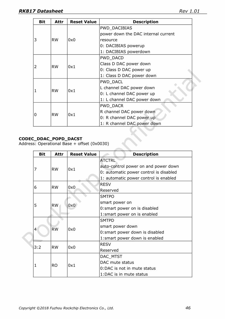
CODEC_DDAC_POPD_DACST Address: Operational Base + offset (0x0030)
Bit Attr Reset Value Description
7 RW 0x1
ATCTRL
auto-control power on and power down
0: automatic power control is disabled
1: automatic power control is enabled
6 RW 0x0 RESV
Reserved
5 RW 0x0
SMTPO
smart power on
0:smart power on is disabled
1:smart power on is enabled
4 RW 0x0
SMTPD
smart power down
0:smart power down is disabled
1:smart power down is enabled
3:2 RW 0x0 RESV
Reserved
1 RO 0x1
DAC_MTST
DAC mute status
0:DAC is not in mute status
1:DAC is in mute status

RK817 Datasheet Rev 1.01
Copyright ©2018 Fuzhou Rockchip Electronics Co., Ltd. 47
Bit Attr Reset Value Description
0 RO 0x0
DAC_PWRST
DAC power status
0:DAC is powered down
1:DAC is powered on
CODEC_DDAC_VOLL
Address: Operational Base + offset (0x0031)
Bit Attr Reset Value Description
7:0 RW 0x00
DACLV
DAC path L-channel Digital Volume Register
0db~-95db,0.375db/step
CODEC_DDAC_VOLR Address: Operational Base + offset (0x0032)
Bit Attr Reset Value Description
7:0 RW 0x00
DACRV
DAC path R-channel Digital Volume Register
0db~-95db,0.375db/step
CODEC_DDAC_SR_LMT0 Address: Operational Base + offset (0x0035)
Bit Attr Reset Value Description
7 RW 0x0
LIMEN
LIMITER enable;
0:disable 1:enable
6 RW 0x0 LIMCHL
0:(left+right)/2 1:independent
5 RW 0x0 DAC_LV_POL
0:negative gain; 1:postive gain
4 RW 0x0 DAC_RV_POL
0:negative gain; 1:postive gain
3 RW 0x0 RESV
Reserved
2:0 RW 0x0
DACSRT
DAC sample rate times
sample rate = 8k/11.025k/12k *
power(2,DACSRT)
CODEC_DDAC_LMT1 Address: Operational Base + offset (0x0036)

RK817 Datasheet Rev 1.01
Copyright ©2018 Fuzhou Rockchip Electronics Co., Ltd. 48
Bit Attr Reset Value Description
7:4 RW 0x0
LIMRRATE
LIMITER Release rate=
8*power(2,LIMRRATE) samples
3:0 RW 0x0
LIMARATE
LIMITER attack rate=8*power(2,LIMARATE)
samples
CODEC_DDAC_LMT2
Address: Operational Base + offset (0x0037)
Bit Attr Reset Value Description
7 RW 0x0 RESV
Reserved
6:4 RW 0x0
LIMMAX
The highest threshold of LIMITER;
000~100:0db~-12db,3db/step;
101~111:-18db~-30db,6db/step;
3 RW 0x0 RESV
Reserved
2:0 RW 0x0 LIMMIN
The lowest threshold of LIMITER;
CODEC_DDAC_MUTE_MIXCTL Address: Operational Base + offset (0x0038)
Bit Attr Reset Value Description
7 RW 0x1 DAC_D_HPF
0:disable HPF;1:enable HPF;
6:5 RW 0x1 DAC_D_HPF_CF
00:80HZ; 01:100HZ; 02:120HZ; 03:140HZ
4 RW 0x0 CLASS_D_MODE
1:CLASS D mode, 0:L/R mode
3 RW 0x0 CLASSD_MODE_L_SEL
0:(L+R)/2; 1:L
2 RW 0x0 RESV
Reserved
1 RW 0x0 MIX_ON
0:mixer disable;1:enable;
0 RW 0x0
DACMT
DAC mute enable
0:DAC mute is disabled
1:DAC mute is enable
CODEC_DDAC_RVOLL Address: Operational Base + offset (0x0039)
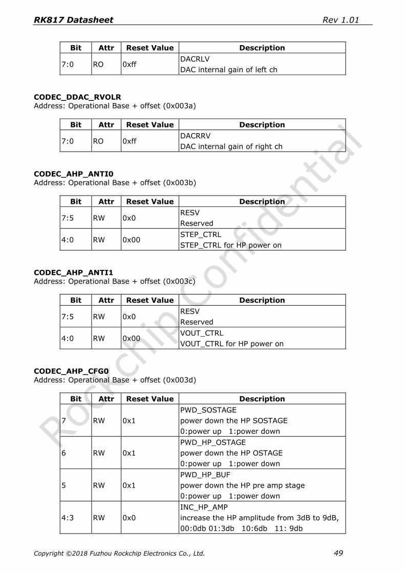
RK817 Datasheet Rev 1.01
Copyright ©2018 Fuzhou Rockchip Electronics Co., Ltd. 49
Bit Attr Reset Value Description
7:0 RO 0xff DACRLV
DAC internal gain of left ch
CODEC_DDAC_RVOLR Address: Operational Base + offset (0x003a)
Bit Attr Reset Value Description
7:0 RO 0xff DACRRV
DAC internal gain of right ch
CODEC_AHP_ANTI0 Address: Operational Base + offset (0x003b)
Bit Attr Reset Value Description
7:5 RW 0x0 RESV
Reserved
4:0 RW 0x00 STEP_CTRL
STEP_CTRL for HP power on
CODEC_AHP_ANTI1 Address: Operational Base + offset (0x003c)
Bit Attr Reset Value Description
7:5 RW 0x0 RESV
Reserved
4:0 RW 0x00 VOUT_CTRL
VOUT_CTRL for HP power on
CODEC_AHP_CFG0
Address: Operational Base + offset (0x003d)
Bit Attr Reset Value Description
7 RW 0x1
PWD_SOSTAGE
power down the HP SOSTAGE
0:power up 1:power down
6 RW 0x1
PWD_HP_OSTAGE
power down the HP OSTAGE
0:power up 1:power down
5 RW 0x1
PWD_HP_BUF
power down the HP pre amp stage
0:power up 1:power down
4:3 RW 0x0
INC_HP_AMP
increase the HP amplitude from 3dB to 9dB,
00:0db 01:3db 10:6db 11: 9db
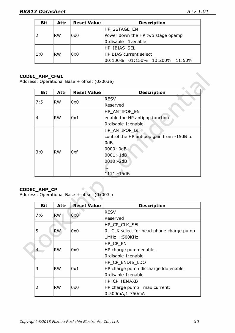
RK817 Datasheet Rev 1.01
Copyright ©2018 Fuzhou Rockchip Electronics Co., Ltd. 50
Bit Attr Reset Value Description
2 RW 0x0
HP_2STAGE_EN
Power down the HP two stage opamp
0:disable 1:enable
1:0 RW 0x0
HP_IBIAS_SEL
HP BIAS current select
00:100% 01:150% 10:200% 11:50%
CODEC_AHP_CFG1
Address: Operational Base + offset (0x003e)
Bit Attr Reset Value Description
7:5 RW 0x0 RESV
Reserved
4 RW 0x1
HP_ANTIPOP_EN
enable the HP antipop function
0:disable 1:enable
3:0 RW 0xf
HP_ANTIPOP_BIT
control the HP antipop gain from -15dB to
0dB
0000: 0dB
0001:-1dB
0010:-2dB
…
1111:-15dB
CODEC_AHP_CP
Address: Operational Base + offset (0x003f)
Bit Attr Reset Value Description
7:6 RW 0x0 RESV
Reserved
5 RW 0x0
HP_CP_CLK_SEL
0:CLK select for head phone charge pump
1MHz :500KHz
4 RW 0x0
HP_CP_EN
HP charge pump enable.
0:disable 1:enable
3 RW 0x1
HP_CP_ENDIS_LDO
HP charge pump discharge ldo enable
0:disable 1:enable
2 RW 0x0
HP_CP_HIMAXB
HP charge pump max current:
0:500mA,1:750mA
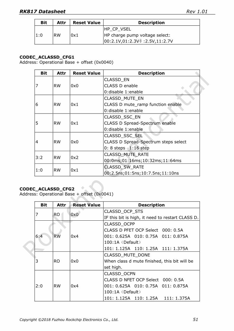
RK817 Datasheet Rev 1.01
Copyright ©2018 Fuzhou Rockchip Electronics Co., Ltd. 51
Bit Attr Reset Value Description
1:0 RW 0x1
HP_CP_VSEL
HP charge pump voltage select:
00:2.1V,01:2.3Vꂺ :2.5V,11:2.7V
CODEC_ACLASSD_CFG1
Address: Operational Base + offset (0x0040)
Bit Attr Reset Value Description
7 RW 0x0
CLASSD_EN
CLASS D enable
0:disable 1:enable
6 RW 0x1
CLASSD_MUTE_EN
CLASS D mute_ramp function enable
0:disable 1:enable
5 RW 0x1
CLASSD_SSC_EN
CLASS D Spread-Spectrum enable
0:disable 1:enable
4 RW 0x0
CLASSD_SSC_SEL
CLASS D Spread-Spectrum steps select
0: 8 steps 1:16 step
3:2 RW 0x2 CLASSD_MUTE_RATE
00:0ms;01:16ms;10:32ms;11:64ms
1:0 RW 0x1 CLASSD_SW_RATE
00:2.5ns;01:5ns;10:7.5ns;11:10ns
CODEC_ACLASSD_CFG2 Address: Operational Base + offset (0x0041)
Bit Attr Reset Value Description
7 RO 0x0 CLASSD_OCP_STS
IF this bit is high, it need to restart CLASS D.
6:4 RW 0x4
CLASSD_OCPP
CLASS D PFET OCP Select 000: 0.5A
001: 0.625A 010: 0.75A 011: 0.875A
100:1A(Default)
101: 1.125A 110: 1.25A 111: 1.375A
3 RO 0x0
CLASSD_MUTE_DONE
When class d mute finished, this bit will be
set high.
2:0 RW 0x4
CLASSD_OCPN
CLASS D NFET OCP Select 000: 0.5A
001: 0.625A 010: 0.75A 011: 0.875A
100:1A(Default)
101: 1.125A 110: 1.25A 111: 1.375A

RK817 Datasheet Rev 1.01
Copyright ©2018 Fuzhou Rockchip Electronics Co., Ltd. 52
CODEC_APLL_CFG0 Address: Operational Base + offset (0x0042)
Bit Attr Reset Value Description
7:4 RW 0x0 RESV
Reserved
3 RW 0x0
PLL_CLKIN_SEL
the PLL input clock select, 0->main clk
1->main clk/2
2 RW 0x1
PLL_OUTDIV_EN
enable PLL VCO output clock divide
0:disable 1:enable
1:0 RW 0x0 PLL_VCO_BANDSEL
PLL VCO working band select
CODEC_APLL_CFG1
Address: Operational Base + offset (0x0043)
Bit Attr Reset Value Description
7:6 RW 0x0 PLL_RES_SEL
PLL filter resistor value select
5:3 RW 0x0 PLL_CUR_SEL
PLL charge-pump working current select
2:0 RW 0x0
PLL_POSDIV_L3
PLL feedback clock divide value select low 3
bits
CODEC_APLL_CFG2
Address: Operational Base + offset (0x0044)
Bit Attr Reset Value Description
7:0 RW 0x30
PLL_POSDIV_H8
PLL feedback clock divide value select high 8
bits
CODEC_APLL_CFG3 Address: Operational Base + offset (0x0045)
Bit Attr Reset Value Description
7:0 RW 0x19 PLL_PREDIV_BIT
PLL input clock pre-divide value select
CODEC_APLL_CFG4 Address: Operational Base + offset (0x0046)

RK817 Datasheet Rev 1.01
Copyright ©2018 Fuzhou Rockchip Electronics Co., Ltd. 53
Bit Attr Reset Value Description
7:4 RW 0x6
PLL_OUTDIV
PLL VCO output clock divide value select
outdiv<3:2>: 00-> divide 5 01-> divide 10
10-> divide 3 11-> divide 6
outdiv<1:0>: 00-> divide 3 01-> divide 1
10-> divide 2 11-> divide 1"
3:0 RW 0x5
PLL_CLK_DIV
PLL divided ratio of PLL_HIGH_clk,
0000->divded 1 and 1111->divided 15
CODEC_APLL_CFG5
Address: Operational Base + offset (0x0047)
Bit Attr Reset Value Description
7:3 RW 0x00 RESV
Reserved
2 RW 0x0
PLL_RESET
reset the total PLL register
0:release reset 1:set reset
1 RW 0x0
PLL_TEST
check the PLL internal VCO control voltage
0:disable 1:enable
0 RW 0x1
PLL_PWD
pll power down
0: PLL power up
1:PLL power down
CODEC_DI2S_CKM Address: Operational Base + offset (0x0048)
Bit Attr Reset Value Description
7:4 RW 0x0 SCK_DIV
F(mclk2x)/F(sclk) - 1
3 RW 0x0
PDM_EN
I2S SDO output delta-sigma ADC 1bit data.
0:disable; 1:enable.
2 RW 0x0
SCK_EN
i2ssclk clock enable, active in master mode.
0:disable 1:enable
1 RW 0x0
SCK_P
sclk polarity
0: normal
1:inverted

RK817 Datasheet Rev 1.01
Copyright ©2018 Fuzhou Rockchip Electronics Co., Ltd. 54
Bit Attr Reset Value Description
0 RW 0x1
I2S_TX_MST
I2S TX module as
0: slave mode 1: master mode
CODEC_DI2S_RSD
Address: Operational Base + offset (0x0049)
Bit Attr Reset Value Description
7:4 RW 0x0 RESV
Reserved
3 RW 0x0 PDM_LR_SEL
0:L; 1:R
2:1 RW 0x0
SCKD_RX
sclk divider for rxlrck generator
00:64 01:128 10:256(01 valid only if lrclk<=
96k, 10 valid only if lrclk<= 48k)
0 RW 0x0
RXRL_P
I2S Rx lrck polarity
0: normal
1:inverted
CODEC_DI2S_RXCR1
Address: Operational Base + offset (0x004a)
Bit Attr Reset Value Description
7 RW 0x0 RESV
Reserved
6 RW 0x0
TFS_RX
Rx transfer mode selector:
0: I2S 1:PCM
5:4 RW 0x0
PBM_RX
Rx PCM bus mode:
00: delay0 01:delay1
10: delay2 11:delay3
3:2 RW 0x0
IBM_RX
Rx I2S bus mode:
00: normal 01:left 10:right
1 RW 0x0
EXRL_RX
Rx exchange right/left channel for rx
0: normal
1:exchange right and left channel
0 RW 0x0 LSB_RX
0: LSB 1:MSB
CODEC_DI2S_RXCR2

RK817 Datasheet Rev 1.01
Copyright ©2018 Fuzhou Rockchip Electronics Co., Ltd. 55
Address: Operational Base + offset (0x004b)
Bit Attr Reset Value Description
7:5 RW 0x0 RESV
Reserved
4:0 RW 0x17
VDW_RX
valid date width
0x17: 24 bits data width; 0x0F: 16 bits data
width; others: reserved
CODEC_DI2S_RXCMD_TSD Address: Operational Base + offset (0x004c)
Bit Attr Reset Value Description
7:6 RW 0x0 RESV
Reserved
5 RW 0x0
RXS
rx transfer start
0: rx stop 1:rx start
4 RW 0x0 RXC
rx transfer clear, high active
3 RW 0x0 RESV
Reserved
2:1 RW 0x0
SCKD_TX
sclk divider for txlrck generator
00:64 01:128 10:256(01 valid only if lrclk<=
96k, 10 valid only if lrclk<= 48k)
0 RW 0x0
TXRL_P
I2S Txlrck polarity
0:normal 1:inverted
CODEC_DI2S_TXCR1 Address: Operational Base + offset (0x004d)
Bit Attr Reset Value Description
7 RW 0x0 RESV
Reserved
6 RW 0x0
TFS_TX
Tx transfer mode selector:
0: I2S 1:PCM
5:4 RW 0x0
PBM_TX
Tx PCM bus mode:
00: delay0 01: delay1
10: delay2
RK817 Datasheet Rev 1.01
Copyright ©2018 Fuzhou Rockchip Electronics Co., Ltd. 56
Bit Attr Reset Value Description
3:2 RW 0x0
IBM_TX
Tx I2S bus mode:
00: normal 01:left 10:right
1 RW 0x0
EXRL_TX
Tx exchange right/left channel for TX
0: normal
1:exchange right and left channel
0 RW 0x0 LSB_TX
0: LSB 1:MSB
CODEC_DI2S_TXCR2 Address: Operational Base + offset (0x004e)
Bit Attr Reset Value Description
7:5 RW 0x0 RESV
Reserved
4:0 RW 0x17
VDW_TX
valid date width
0x17: 24 bits data width; 0x0F: 16 bits data
width; others: reserved
CODEC_DI2S_TXCR3_TXCMD
Address: Operational Base + offset (0x004f)
Bit Attr Reset Value Description
7 RW 0x0
TXS
tx transfer start
0: tx stop 1:tx start
6 RW 0x0 TXC
tx transfer clear, high active
5:0 RW 0x00
RCNT_TX
right justified counter for I2S right justified
slave mode only
gas_gauge_ADC_CONFIG0 Address: Operational Base + offset (0x0050)
Bit Attr Reset Value Description
7 RW 0x1
GG_EN
GG_EN: Gasgauge module enable bit
0:disable 1: enable
6 RW 0x0
SYS_VOL_ADC_EN
SYS_VOL_ADC_EN: if GG_EN=0, then the
ADC of SYS voltage controlled by the bit
0:disable 1:enable

RK817 Datasheet Rev 1.01
Copyright ©2018 Fuzhou Rockchip Electronics Co., Ltd. 57
Bit Attr Reset Value Description
5 RW 0x0
TS_ADC_EN
TS_ADC_EN: if GG_EN=0, the ADC of TS1
controlled by the bit
0:disable 1:enable
4 RW 0x0
USB_VOL_ADC_EN
USB_VOL_ADC_EN: if GG_EN=0, the ADC
of USB voltage by the bit
0:disable 1:enable
3 RW 0x1
BAT_VOL_ADC_EN
BAT_VOL_ADC_EN: if GG_EN=0, then the
ADC of BAT voltage controlled by the bit
0:disable 1:enable
2 RW 0x1
BAT_CUR_ADC_EN
BAT_CUR_ADC_EN: if GG_EN=0, then the
ADC of BAT current controlled by the bit
0:disable 1:enable
1 RW 0x0 RESV
RESV:Reserve
0 RW 0x0
ADC_SLP_RATE
ADC_SLP_RATE: the ADC sample rate:
0:512; 1:1024
gas_gauge_ADC_CONFIG1 Address: Operational Base + offset (0x0055)
Bit Attr Reset Value Description
7 RC 0x0
VOL_CUR_CALIB_UPD
VOL_CUR_CALIB_UPD: The voltage ADC and
current ADC calibration finished status
0:not finished 1:finished
(Write “1” to clear)
6 RW 0x0 RESV
RESV:Reserve
5:4 RW 0x3
VOL_ADC_TSCUR_SEL
VOL_ADC_TSCUR_SEL: TS pin flow out
current in active state
00:20uA 01:40uA 10:60uA 11:80uA
3 RW 0x0
TS_FUN
TS_FUN: TS pin function selection
0:source current to TS pin
1:external voltage input directly
2 RW 0x0 RESV
RESV:Reserve

RK817 Datasheet Rev 1.01
Copyright ©2018 Fuzhou Rockchip Electronics Co., Ltd. 58
Bit Attr Reset Value Description
1:0 RW 0x0
RLX_CUR_FILTER
RLX_CUR_FILTER:Relax mode enter
threshold filter.
00:4S; 01:1S; 10:2S; 11:8S;
gas_gauge_GG_CON
Address: Operational Base + offset (0x0056)
Bit Attr Reset Value Description
7:6 RW 0x1
RLX_SPT
RLX_SPT: relax mode voltage sampling
interval time
T_RELAX: Relax mode enter and quit time
00:8min 01:16min 10:32min 11:48min
5:4 RW 0x0
ADC_OFF_CAL_INTERV
ADC_OFF_CAL_INTERV<1:0>: ADC offset
calibration interval time
00:8min 01:16min 10:32min 11:48min
3:2 RW 0x1
FRAME_SMP_INTERV
FRAME_SMP_INTERV<1:0>:Data frame
sample interval in the sleep state(Unit:S)
00:0S 01:1S 10:2S 11:3S
1 RW 0x0
VOL_OUT_MOD
VOL_OUT_MOD: Voltageoutput mode
0:Average Voltage 1:Instant Voltage
0 RW 0x0
CUR_OUT_MOD
CUR_OUT_MOD: Current output mode
0:Average Current 1:Instant Current
gas_gauge_GG_STS Address: Operational Base + offset (0x0057)
Bit Attr Reset Value Description
7 RO 0x0
OCV_STS
OCV_STS: OCV mode status.
1: ocv mode;
0: null ocv mode.
6 RO 0x0
TERM_UPD
TERM_UPD: Flag bit for Q_TERM update
0:NOT 1:YES
5 RW 0x0
QMAX_UPD_SOFT
QMAX_UPD_SOFT: software Flag bit for
QMAX update
0:NOT 1:YES

RK817 Datasheet Rev 1.01
Copyright ©2018 Fuzhou Rockchip Electronics Co., Ltd. 59
Bit Attr Reset Value Description
4 RO 0x0
BAT_CON
BAT_CON: battery first connection, edge
trigger
0:NOT 1:YES
3 RO 0x0
RELAX_VOL1_UPD
RELAX_VOL1_UPD: battery voltage1
updated in relax status
0:NOT 1:YES
2 RO 0x0
RELAX_VOL2_UPD
RELAX_VOL2_UPD: battery voltage2
updated in relax status
0:NOT 1:YES
1 RO 0x0
RELAX_STS
RELAX_STS: battery coming into relax status
0:NOT 1:YES
0 RO 0x0
OCV_UPD
OCV_UPD: Flag bit for OCV update
0:NOT 1:YES
gas_gauge_RELAX_THRE_H
Address: Operational Base + offset (0x0058)
Bit Attr Reset Value Description
7:0 RW 0x00
RELAX_THRE_CUR
RELAX_THRE_CUR: relax mode threshold
current set.<15:8>
gas_gauge_RELAX_THRE_L Address: Operational Base + offset (0x0059)
Bit Attr Reset Value Description
7:0 RW 0x60
RELAX_THRE_CUR
RELAX_THRE_CUR: relax mode threshold
current set. <7:0>
gas_gauge_RELAX_VOL1_H Address: Operational Base + offset (0x005a)
Bit Attr Reset Value Description
7:0 RO 0x00
RELAX_VOL1_H
RELAX_VOL1_H<15:8>: relax 1st mode
voltage
gas_gauge_RELAX_VOL1_L Address: Operational Base + offset (0x005b)

RK817 Datasheet Rev 1.01
Copyright ©2018 Fuzhou Rockchip Electronics Co., Ltd. 60
Bit Attr Reset Value Description
7:0 RO 0x00
RELAX_VOL1_L
RELAX_VOL1_L<7:0>: relax 1st mode
voltage
gas_gauge_RELAX_VOL2_H Address: Operational Base + offset (0x005c)
Bit Attr Reset Value Description
7:0 RO 0x00
RELAX_VOL2
RELAX_VOL2<15:8>: relax 2nd mode
voltage
gas_gauge_RELAX_VOL2_L Address: Operational Base + offset (0x005d)
Bit Attr Reset Value Description
7:0 RO 0x00
RELAX_VOL2
RELAX_VOL2<7:0>: relax 2nd mode
voltage
gas_gauge_RELAX_CUR1_H
Address: Operational Base + offset (0x005e)
Bit Attr Reset Value Description
7:0 RO 0x00 RELAX_CUR1
RELAX_CUR1<15:8>:relax 1st mode current
gas_gauge_RELAX_CUR1_L Address: Operational Base + offset (0x005f)
Bit Attr Reset Value Description
7:0 RO 0x00 RELAX_CUR1
RELAX_CUR1<7:0>: relax 1st mode current
gas_gauge_RELAX_CUR2_H
Address: Operational Base + offset (0x0060)
Bit Attr Reset Value Description
7:0 RO 0x00
RELAX_CUR2
RELAX_CUR2<15:8>: relax 2nd mode
current
gas_gauge_RELAX_CUR2_L Address: Operational Base + offset (0x0061)
RK817 Datasheet Rev 1.01
Copyright ©2018 Fuzhou Rockchip Electronics Co., Ltd. 61
Bit Attr Reset Value Description
7:0 RO 0x00 RELAX_CUR2
RELAX_CUR2<7:0>: relax 2nd mode current
gas_gauge_OCV_THRE_VOL Address: Operational Base + offset (0x0062)
Bit Attr Reset Value Description
7:0 RW 0x00
OCV_THRE_VOL
OCV_THRE_VOL:OCV mode threshold.
00:0.5mV; 01:1mV;
02:1.5mV…..FF:127.5mV
gas_gauge_OCV_VOL_H Address: Operational Base + offset (0x0063)
Bit Attr Reset Value Description
7:0 RO 0x00 OCV_VOL_REG
OCV_VOL_REG<15:8>: OCV voltage
gas_gauge_OCV_VOL_L
Address: Operational Base + offset (0x0064)
Bit Attr Reset Value Description
7:0 RO 0x00 OCV_VOL_REG
OCV_VOL_REG<7:0>:OCV voltage
gas_gauge_OCV_VOL0_H Address: Operational Base + offset (0x0065)
Bit Attr Reset Value Description
7:0 RO 0x00 OCV_VOL0_REG
OCV_VOL0_REG<15:8>:OCV voltage 0
gas_gauge_OCV_VOL0_L
Address: Operational Base + offset (0x0066)
Bit Attr Reset Value Description
7:0 RO 0x00 OCV_VOL0_REG
OCV_VOL0_REG<7:0>:OCV voltage 0
gas_gauge_OCV_CUR_H Address: Operational Base + offset (0x0067)

RK817 Datasheet Rev 1.01
Copyright ©2018 Fuzhou Rockchip Electronics Co., Ltd. 62
Bit Attr Reset Value Description
7:0 RO 0x00 OCV_CUR_REG
OCV_CUR_REG<15:8>:OCV current
gas_gauge_OCV_CUR_L
Address: Operational Base + offset (0x0068)
Bit Attr Reset Value Description
7:0 RO 0x00 OCV_CUR_REG
OCV_CUR_REG<7:0>:OCV current
gas_gauge_OCV_CUR0_H Address: Operational Base + offset (0x0069)
Bit Attr Reset Value Description
7:0 RO 0x00 OCV_CUR0_REG
OCV_CUR0_REG<15:8>: OCV current 0
gas_gauge_OCV_CUR0_L Address: Operational Base + offset (0x006a)
Bit Attr Reset Value Description
7:0 RO 0x00 OCV_CUR0_REG
OCV_CUR0_REG<7:0>: OCV current 0
gas_gauge_PWRON_VOL_H Address: Operational Base + offset (0x006b)
Bit Attr Reset Value Description
7:0 RO 0x00
PWRON_VOL_REG
PWRON_VOL_REG<15:8>: power on bat
voltage
gas_gauge_PWRON_VOL_L Address: Operational Base + offset (0x006c)
Bit Attr Reset Value Description
7:0 RO 0x00
PWRON_VOL_REG
PWRON_VOL_REG<7:0>: power on bat
voltage
gas_gauge_PWRON_CUR_H
Address: Operational Base + offset (0x006d)

RK817 Datasheet Rev 1.01
Copyright ©2018 Fuzhou Rockchip Electronics Co., Ltd. 63
Bit Attr Reset Value Description
7:0 RO 0x00
PWRON_CUR_REG
PWRON_CUR_REG<15:8>: power on bat
current
gas_gauge_PWRON_CUR_L
Address: Operational Base + offset (0x006e)
Bit Attr Reset Value Description
7:0 RO 0x00
PWRON_CUR_REG
PWRON_CUR_REG<7:0>: power on bat
current
gas_gauge_OFF_CNT Address: Operational Base + offset (0x006f)
Bit Attr Reset Value Description
7:0 RW 0x00 OFF_CNT
OFF_CNT<7:0>: power off time
gas_gauge_Q_INIT_H3 Address: Operational Base + offset (0x0070)
Bit Attr Reset Value Description
7:0 RW 0x00 Q_INIT
Q_INIT<31:24>:power off time
gas_gauge_Q_INIT_H2 Address: Operational Base + offset (0x0071)
Bit Attr Reset Value Description
7:0 RW 0x00 Q_INIT
Q_INIT<23:16>:power off time
gas_gauge_Q_INIT_L1 Address: Operational Base + offset (0x0072)
Bit Attr Reset Value Description
7:0 RW 0x00 Q_INIT
Q_INIT<15:8>:power off time
gas_gauge_Q_INIT_L0
Address: Operational Base + offset (0x0073)

RK817 Datasheet Rev 1.01
Copyright ©2018 Fuzhou Rockchip Electronics Co., Ltd. 64
Bit Attr Reset Value Description
7:0 RW 0x00 Q_INIT
Q_INIT<7:0>:power off time
gas_gauge_Q_PRES_H3
Address: Operational Base + offset (0x0074)
Bit Attr Reset Value Description
7:0 RO 0x00 Q_PRES
Q_PRES<31:24>:Coulomp value
gas_gauge_Q_PRES_H2 Address: Operational Base + offset (0x0075)
Bit Attr Reset Value Description
7:0 RO 0x00 Q_PRES
Q_PRES<23:16>:Coulomp value
gas_gauge_Q_PRES_L1 Address: Operational Base + offset (0x0076)
Bit Attr Reset Value Description
7:0 RO 0x00 Q_PRES
Q_PRES<15:8>:Coulomp value
gas_gauge_Q_PRES_L0 Address: Operational Base + offset (0x0077)
Bit Attr Reset Value Description
7:0 RO 0x00 Q_PRES
Q_PRES<7:0>:Coulomp value
gas_gauge_BAT_VOL_H Address: Operational Base + offset (0x0078)
Bit Attr Reset Value Description
7:0 RO 0x00 BAT_VOL
BAT_VOL<15:8>: bat voltage
gas_gauge_BAT_VOL_L
Address: Operational Base + offset (0x0079)
Bit Attr Reset Value Description
7:0 RO 0x00 BAT_VOL
BAT_VOL<7:0>:bat voltage

RK817 Datasheet Rev 1.01
Copyright ©2018 Fuzhou Rockchip Electronics Co., Ltd. 65
gas_gauge_BAT_CUR_H Address: Operational Base + offset (0x007a)
Bit Attr Reset Value Description
7:0 RO 0x00 BAT_CUR
BAT_CUR<15:8>:battery current
gas_gauge_BAT_CUR Address: Operational Base + offset (0x007b)
Bit Attr Reset Value Description
7:0 RO 0x00 BAT_CUR
BAT_CUR<7:0>:BAT_CUR: battery current
gas_gauge_BAT_TS_H Address: Operational Base + offset (0x007c)
Bit Attr Reset Value Description
7:0 RO 0x00 BAT_TS
BAT_TS<15:8>:TS ADC value
gas_gauge_BAT_TS_L
Address: Operational Base + offset (0x007d)
Bit Attr Reset Value Description
7:0 RO 0x00 BAT_TS
BAT_TS<7:0>: TS ADC value
gas_gauge_USB_VOL_H Address: Operational Base + offset (0x007e)
Bit Attr Reset Value Description
7:0 RO 0x00 USB_VOL
USB_VOL<15:8>:USB voltage value
gas_gauge_USB_VOL_L
Address: Operational Base + offset (0x007f)
Bit Attr Reset Value Description
7:0 RO 0x00 USB_VOL
USB_VOL<7:0>:USB voltage value
gas_gauge_SYS_VOL_H Address: Operational Base + offset (0x0080)

RK817 Datasheet Rev 1.01
Copyright ©2018 Fuzhou Rockchip Electronics Co., Ltd. 66
Bit Attr Reset Value Description
7:0 RO 0x00 SYS_VOL
SYS_VOL<15:8>: SYS voltage value
gas_gauge_SYS_VOL_L
Address: Operational Base + offset (0x0081)
Bit Attr Reset Value Description
7:0 RO 0x00 SYS_VOL
SYS_VOL<7:0>:SYS voltage value
gas_gauge_Q_MAX_H3 Address: Operational Base + offset (0x0082)
Bit Attr Reset Value Description
7:0 RW 0x00 Q_MAX
Q_MAX<31:24>:Qmax value
gas_gauge_Q_MAX_H2 Address: Operational Base + offset (0x0083)
Bit Attr Reset Value Description
7:0 RW 0x00 Q_MAX
Q_MAX<23:16>:Qmax value
gas_gauge_Q_MAX_L1 Address: Operational Base + offset (0x0084)
Bit Attr Reset Value Description
7:0 RW 0x00 Q_MAX
Q_MAX<15:8>:Qmax value
gas_gauge_Q_MAX_L0 Address: Operational Base + offset (0x0085)
Bit Attr Reset Value Description
7:0 RW 0x00 Q_MAX
Q_MAX<7:0>:Qmax value
gas_gauge_Q_TERM_H3
Address: Operational Base + offset (0x0086)
Bit Attr Reset Value Description
7:0 RO 0x00
Q_TERM
Q_TERM<31:24>:charge terminal Coulomp
value

RK817 Datasheet Rev 1.01
Copyright ©2018 Fuzhou Rockchip Electronics Co., Ltd. 67
gas_gauge_Q_TERM_H2
Address: Operational Base + offset (0x0087)
Bit Attr Reset Value Description
7:0 RO 0x00
Q_TERM
Q_TERM<23:16>:charge terminal Coulomp
value
gas_gauge_Q_TERM_L1 Address: Operational Base + offset (0x0088)
Bit Attr Reset Value Description
7:0 RO 0x00
Q_TERM
Q_TERM<15:8>:charge terminal Coulomp
value
gas_gauge_Q_TERM_L0
Address: Operational Base + offset (0x0089)
Bit Attr Reset Value Description
7:0 RO 0x00
Q_TERM
Q_TERM<7:0>:charge terminal Coulomp
value
gas_gauge_Q_OCV_H3 Address: Operational Base + offset (0x008a)
Bit Attr Reset Value Description
7:0 RO 0x00 Q_OCV
Q_OCV<31:24>:OCV update Coulomp value
gas_gauge_Q_OCV_H2
Address: Operational Base + offset (0x008b)
Bit Attr Reset Value Description
7:0 RO 0x00 Q_OCV
Q_OCV<23:16>:OCV update Coulomp value
gas_gauge_Q_OCV_L1 Address: Operational Base + offset (0x008c)
Bit Attr Reset Value Description
7:0 RO 0x00 Q_OCV
Q_OCV<15:8>:OCV update Coulomp value

RK817 Datasheet Rev 1.01
Copyright ©2018 Fuzhou Rockchip Electronics Co., Ltd. 68
gas_gauge_Q_OCV_L0 Address: Operational Base + offset (0x008d)
Bit Attr Reset Value Description
7:0 RO 0x00 Q_OCV
Q_OCV<7:0>:OCV update Coulomp value
gas_gauge_OCV_CNT Address: Operational Base + offset (0x008e)
Bit Attr Reset Value Description
7:0 RW 0x00 OCV_CNT
OCV_CNT<7:0>: two OCV time interval
gas_gauge_SLEEP_CON_SAMP_CUR_H Address: Operational Base + offset (0x008f)
Bit Attr Reset Value Description
7:0 RW 0x00
SLEEP_CON_SAMP_CUR
SLEEP_CON_SAMP_CUR<15:8>:SLEEP
mode,When the current is greater than the
set value, it is sampled once again, until it is
less than the set value, and the value is
updated to the RELAX register
gas_gauge_SLEEP_CON_SAMP_CUR
Address: Operational Base + offset (0x0090)
Bit Attr Reset Value Description
7:0 RW 0x60
SLEEP_CON_SAMP_CUR
SLEEP_CON_SAMP_CUR<7:0>: SLEEP
mode,When the current is greater than the
set value, it is sampled once again, until it is
less than the set value, and the value is
updated to the RELAX register
gas_gauge_CAL_OFFSET_H Address: Operational Base + offset (0x0091)
Bit Attr Reset Value Description
7:0 RW 0x7f
CAL_OFFSET_REG
CAL_OFFSET_REG<15:8>: PCB current
offset value high bit
gas_gauge_CAL_OFFSET_L

RK817 Datasheet Rev 1.01
Copyright ©2018 Fuzhou Rockchip Electronics Co., Ltd. 69
Address: Operational Base + offset (0x0092)
Bit Attr Reset Value Description
7:0 RW 0xff
CAL_OFFSET_REG
CAL_OFFSET_REG<7:0>: PCB current offset
value low bit
gas_gauge_VCALIB0_H Address: Operational Base + offset (0x0093)
Bit Attr Reset Value Description
7:0 RO 0x00
VCALIB0
VCALIB0<15:8>:Voltage0 offset value for AP
to calculate offset error and gain error
gas_gauge_VCALIB0_L
Address: Operational Base + offset (0x0094)
Bit Attr Reset Value Description
7:0 RO 0x00
VCALIB0
VCALIB0<7:0>:Voltage0 offset value for AP
to calculate offset error and gain error
gas_gauge_VCALIB1_H Address: Operational Base + offset (0x0095)
Bit Attr Reset Value Description
7:0 RO 0x00
VCALIB1
VCALIB1<15:8>:Voltage1 offset value for AP
to calculate offset error and gain error
gas_gauge_VCALIB1_L
Address: Operational Base + offset (0x0096)
Bit Attr Reset Value Description
7:0 RO 0x00
VCALIB1
VCALIB1<7:0>:Voltage1 offset value for AP
to calculate offset error and gain error
gas_gauge_IOFFSET_H Address: Operational Base + offset (0x0097)
Bit Attr Reset Value Description
7:0 RO 0x00
IOFFSET
IOFFSET<15:8>:Current offset value
calculated

RK817 Datasheet Rev 1.01
Copyright ©2018 Fuzhou Rockchip Electronics Co., Ltd. 70
gas_gauge_IOFFSET_L
Address: Operational Base + offset (0x0098)
Bit Attr Reset Value Description
7:0 RO 0x00
IOFFSET
IOFFSET<7:0>:Current offset value
calculated
gas_gauge_BAT_R0 Address: Operational Base + offset (0x0099)
Bit Attr Reset Value Description
7:0 RW 0x00 BAT_R0
BAT_R0<7:0>:BAT resistance
gas_gauge_BAT_R1
Address: Operational Base + offset (0x009a)
Bit Attr Reset Value Description
7:0 RW 0x00 BAT_R1
BAT_R1<7:0>:BAT resistance
gas_gauge_BAT_R2 Address: Operational Base + offset (0x009b)
Bit Attr Reset Value Description
7:0 RW 0x00 BAT_R2
BAT_R2<7:0>:BAT resistance
gas_gauge_BAT_R3
Address: Operational Base + offset (0x009c)
Bit Attr Reset Value Description
7:0 RW 0x00 BAT_R3
BAT_R3<7:0>:BAT resistance
gas_gauge_DATA0 Address: Operational Base + offset (0x009d)
Bit Attr Reset Value Description
7:0 RW 0x00 DATA
DATA<7:0>:data for AP
gas_gauge_DATA1

RK817 Datasheet Rev 1.01
Copyright ©2018 Fuzhou Rockchip Electronics Co., Ltd. 71
Address: Operational Base + offset (0x009e)
Bit Attr Reset Value Description
7:0 RW 0x00 DATA
DATA<7:0>:data for AP
gas_gauge_DATA2 Address: Operational Base + offset (0x009f)
Bit Attr Reset Value Description
7:0 RW 0x00 DATA
DATA<7:0>:data for AP
gas_gauge_DATA3
Address: Operational Base + offset (0x00a0)
Bit Attr Reset Value Description
7:0 RW 0x00 DATA
DATA<7:0>:data for AP
gas_gauge_DATA4 Address: Operational Base + offset (0x00a1)
Bit Attr Reset Value Description
7:0 RW 0x00 DATA
DATA<7:0>:data for AP
gas_gauge_DATA5
Address: Operational Base + offset (0x00a2)
Bit Attr Reset Value Description
7:0 RW 0x00 DATA
DATA<7:0>:data for AP
gas_gauge_DATA6 Address: Operational Base + offset (0x00a3)
Bit Attr Reset Value Description
7:0 RW 0x00 DATA
DATA<7:0>:data for AP
gas_gauge_DATA7 Address: Operational Base + offset (0x00a4)

RK817 Datasheet Rev 1.01
Copyright ©2018 Fuzhou Rockchip Electronics Co., Ltd. 72
Bit Attr Reset Value Description
7:0 RW 0x00 DATA
DATA<7:0>:data for AP
gas_gauge_DATA8
Address: Operational Base + offset (0x00a5)
Bit Attr Reset Value Description
7:0 RW 0x00 DATA
DATA<7:0>:data for AP
gas_gauge_DATA9 Address: Operational Base + offset (0x00a6)
Bit Attr Reset Value Description
7:0 RW 0x00 DATA
DATA<7:0>:data for AP
gas_gauge_DATA10 Address: Operational Base + offset (0x00a7)
Bit Attr Reset Value Description
7:0 RW 0x00 DATA
DATA<7:0>:data for AP
gas_gauge_DATA11 Address: Operational Base + offset (0x00a8)
Bit Attr Reset Value Description
7:0 RW 0x00 DATA
DATA<7:0>:data for AP
gas_gauge_VOL_ADC_B3 Address: Operational Base + offset (0x00a9)
Bit Attr Reset Value Description
7:0 RO OTP
VOL_ADC_B
VOL_ADC_B<31:24>:
default:OTP
gas_gauge_VOL_ADC_B2
Address: Operational Base + offset (0x00aa) Register0000 Abstract

RK817 Datasheet Rev 1.01
Copyright ©2018 Fuzhou Rockchip Electronics Co., Ltd. 73
Bit Attr Reset Value Description
7:0 RO OTP
VOL_ADC_B
VOL_ADC_B<23:16>
default: OTP
gas_gauge_VOL_ADC_B1
Address: Operational Base + offset (0x00ab) Register0000 Abstract
Bit Attr Reset Value Description
7:0 RO OTP
VOL_ADC_B
VOL_ADC_B<15:8>
default: OTP
gas_gauge_VOL_ADC_B_7_0 Address: Operational Base + offset (0x00ac) Register0000 Abstract
Bit Attr Reset Value Description
7:0 RO OTP
VOL_ADC_B0
VOL_ADC_B<7:0>
default: OTP
gas_gauge_CUR_ADC_K3 Address: Operational Base + offset (0x00ad)
Bit Attr Reset Value Description
7:0 RO OTP
CUR_ADC_K
CUR_ADC_K<31:24>
default: OTP
gas_gauge_CUR_ADC_K2 Address: Operational Base + offset (0x00ae)
Bit Attr Reset Value Description
7:0 RO OTP
CUR_ADC_K
CUR_ADC_K<23:16>
default: OTP
gas_gauge_CUR_ADC_K1 Address: Operational Base + offset (0x00af)
Bit Attr Reset Value Description
7:0 RO OTP
CUR_ADC_K
CUR_ADC_K<15:8>
default: OTP

RK817 Datasheet Rev 1.01
Copyright ©2018 Fuzhou Rockchip Electronics Co., Ltd. 74
gas_gauge_CUR_ADC_K0 Address: Operational Base + offset (0x00b0)
Bit Attr Reset Value Description
7:0 RO OTP
CUR_ADC_K0
CUR_ADC_K<7:0>
default: OTP
PMIC_POWER_EN0 Address: Operational Base + offset (0x00b1)
Bit Attr Reset Value Description
7 RW 0x0
BUCK4_EN_MASK
BUCK4_EN_MASK: MUST write them to "1" if
want to change corresponding BUCK4_EN
bit,The BUCK4_EN_MASK bits should be
clear when BUCK4_EN bits have been
written.
6 RW 0x0
BUCK3_EN_MASK
BUCK3_EN_MASK: MUST write them to "1" if
want to change corresponding BUCK3_EN
bit,The BUCK3_EN_MASK bits should be
clear when BUCK3_EN bits have been
written.
5 RW 0x0
BUCK2_EN_MASK
BUCK2_EN_MASK: MUST write them to "1" if
want to change corresponding BUCK2_EN
bit,The BUCK2_EN_MASK bits should be
clear when BUCK2_EN bits have been
written.
4 RW 0x0
BUCK1_EN_MASK
BUCK1_EN_MASK: MUST write them to "1" if
want to change corresponding BUCK1_EN
bit,The BUCK1_EN_MASK bits should be
clear when BUCK1_EN bits have been
written.
3 RW OTP
BUCK4_EN
BUCK4_EN: BUCK4 enable in active mode
1, Enable
0, Disable
the default value is set by otp
reset by power down or RST.
2 RW OTP
BUCK3_EN
BUCK3_EN: BUCK3 enable in active mode
1, Enable
0, Disable
the default value is set by otp
reset by power down or RST.

RK817 Datasheet Rev 1.01
Copyright ©2018 Fuzhou Rockchip Electronics Co., Ltd. 75
Bit Attr Reset Value Description
1 RW OTP
BUCK2_EN
BUCK2_EN: BUCK2 enable in active mode
1, Enable
0, Disable
the default value is set by otp
reset by power down or RST.
0 RW OTP
BUCK1_EN
BUCK1_EN: BUCK1 enable in active mode
1, Enable
0, Disable
the default value is set by otp
reset by power down or RST.
PMIC_POWER_EN1
Address: Operational Base + offset (0x00b2)
Bit Attr Reset Value Description
7 RW 0x0
LDO4_EN_MASK
LDO4_EN_MASK: MUST write them to "1" if
want to change corresponding LDO4_EN
bit,The LDO4_EN_MASK bits should be
clear when LDO4_EN bits have been written.
6 RW 0x0
LDO3_EN_MASK
LDO3_EN_MASK: MUST write them to "1" if
want to change corresponding LDO3_EN
bit,The LDO3_EN_MASK bits should be
clear when LDO3_EN bits have been written.
5 RW 0x0
LDO2_EN_MASK
LDO2_EN_MASK: MUST write them to "1" if
want to change corresponding LDO2_EN
bit,The LDO2_EN_MASK bits should be
clear when LDO2_EN bits have been written.
4 RW 0x0
LDO1_EN_MASK
LDO1_EN_MASK: MUST write them to "1" if
want to change corresponding LDO1_EN
bit,The LDO1_EN_MASK bits should be
clear when LDO1_EN bits have been written.
3 RW OTP
LDO4_EN
LDO4_EN: LDO4 enable in active mode
1, Enable
0, Disable
the default value is set by otp
reset by power down or RST.

RK817 Datasheet Rev 1.01
Copyright ©2018 Fuzhou Rockchip Electronics Co., Ltd. 76
Bit Attr Reset Value Description
2 RW OTP
LDO3_EN
LDO3_EN: LDO3 enable in active mode
1, Enable
0, Disable
the default value is set by otp
reset by power down or RST.
1 RW OTP
LDO2_EN
LDO2_EN: LDO2 enable in active mode
1, Enable
0, Disable
the default value is set by otp
reset by power down or RST.
0 RW OTP
LDO1_EN
LDO1_EN: LDO1 enable in active mode
1, Enable
0, Disable
the default value is set by otp
reset by power down or RST.
PMIC_POWER_EN2 Address: Operational Base + offset (0x00b3)
Bit Attr Reset Value Description
7 RW 0x0
LDO8_EN_MASK
LDO8_EN_MASK: MUST write them to "1" if
want to change corresponding LDO8_EN
bit,The LDO8_EN_MASK bits should be
clear when LDO8_EN bits have been written.
6 RW 0x0
LDO7_EN_MASK
LDO7_EN_MASK: MUST write them to "1" if
want to change corresponding LDO7_EN
bit,The LDO7_EN_MASK bits should be
clear when LDO7_EN bits have been written.
5 RW 0x0
LDO6_EN_MASK
LDO6_EN_MASK: MUST write them to "1" if
want to change corresponding LDO6_EN
bit,The LDO6_EN_MASK bits should be
clear when LDO6_EN bits have been written.
4 RW 0x0
LDO5_EN_MASK
LDO5_EN_MASK: MUST write them to "1" if
want to change corresponding LDO5_EN
bit,The LDO5_EN_MASK bits should be
clear when LDO5_EN bits have been written.
RK817 Datasheet Rev 1.01
Copyright ©2018 Fuzhou Rockchip Electronics Co., Ltd. 77
Bit Attr Reset Value Description
3 RW OTP
LDO8_EN
LDO8_EN: LDO8 enable in active mode
1, Enable
0, Disable
the default value is set by otp
reset by power down or RST.
2 RW OTP
LDO7_EN
LDO7_EN: LDO7 enable in active mode
1, Enable
0, Disable
the default value is set by otp
reset by power down or RST.
1 RW OTP
LDO6_EN
LDO6_EN: LDO6 enable in active mode
1, Enable
0, Disable
the default value is set by otp
reset by power down or RST.
0 RW OTP
LDO5_EN
LDO5_EN: LDO5 enable in active mode
1, Enable
0, Disable
the default value is set by otp
reset by power down or RST.
PMIC_POWER_EN3 Address: Operational Base + offset (0x00b4)
Bit Attr Reset Value Description
7 RW 0x0 RESV
RESV:Reserve
6 RW 0x0
OTG_EN_MASK
OTG_EN _MASK : MUST write them to "1" if
want to change corresponding OTG_EN bit,
The OTG_EN_MASK bits should be clear
when OTG_EN bits have been written.
5 RW 0x0
BOOST_EN_MASK
BOOST_EN _MASK : MUST write them to "1"
if want to change corresponding BOOST_EN
bit,The BOOST_EN_MASK bits should be
clear when BOOST_EN bits have been
written.

RK817 Datasheet Rev 1.01
Copyright ©2018 Fuzhou Rockchip Electronics Co., Ltd. 78
Bit Attr Reset Value Description
4 RW 0x0
LDO9_EN_MASK
LDO9_EN_MASK: MUST write them to "1" if
want to change corresponding LDO9_EN
bit,The LDO9_EN_MASK bits should be
clear when LDO9_EN bits have been written.
3 RW 0x0 RESV
RESV: Reserve
2 RW OTP
OTG_EN
OTG_EN : OTG enable in active mode
1, Enable
0, Disable
the default value is set by otp
reset by power down or RST.
1 RW OTP
BOOST_EN
BOOST_EN : BOOST enable in active mode
1, Enable
0, Disable
the default value is set by otp
reset by power down or RST.
0 RW OTP
LDO9_EN
LDO9_EN: LDO9 enable in active mode
1, Enable
0, Disable
the default value is set by otp
reset by power down or RST.
PMIC_POWER_SLP_EN0 Address: Operational Base + offset (0x00b5)
Bit Attr Reset Value Description
7 RW 0x0 RESV
RESV:Reserve
6 RW OTP
OTG_SLP_EN
OTG_SLP_EN: OTG enable in SLEEP mode
1, Enable
0, Disable
the default value is set by otp
reset by power down or RST.
5 RW OTP
BOOST_SLP_EN
BOOST_SLP_EN: BOOST enable in SLEEP
mode
1, Enable
0, Disable
the default value is set by otp
reset by power down or RST.

RK817 Datasheet Rev 1.01
Copyright ©2018 Fuzhou Rockchip Electronics Co., Ltd. 79
Bit Attr Reset Value Description
4 RW OTP
LDO9_SLP_EN
LDO9_SLP_EN: LDO9 enable in SLEEP mode
1, Enable
0, Disable
the default value is set by otp
reset by power down or RST.
3 RW OTP
BUCK4_SLP_EN
BUCK4_SLP_EN: BUCK4 enable in SLEEP
mode
1, Enable
0, Disable
the default value is set by otp
reset by power down or RST.
2 RW OTP
BUCK3_SLP_EN
BUCK3_SLP_EN: BUCK3 enable in SLEEP
mode
1, Enable
0, Disable
the default value is set by otp
reset by power down or RST.
1 RW OTP
BUCK2_SLP_EN
BUCK2_SLP_EN: BUCK2 enable in SLEEP
mode
1, Enable
0, Disable
the default value is set by otp
reset by power down or RST.
0 RW OTP
BUCK1_SLP_EN
BUCK1_SLP_EN: BUCK1 enable in SLEEP
mode
1, Enable
0, Disable
the default value is set by otp
reset by power down or RST.
PMIC_POWER_SLP_EN1 Address: Operational Base + offset (0x00b6)
Bit Attr Reset Value Description
7 RW OTP
LDO8_SLP_EN
LDO8_SLP_EN: LDO8 enable in SLEEP mode
1, Enable
0, Disable
the default value is set by otp
reset by power down or RST.

RK817 Datasheet Rev 1.01
Copyright ©2018 Fuzhou Rockchip Electronics Co., Ltd. 80
Bit Attr Reset Value Description
6 RW OTP
LDO7_SLP_EN
LDO7_SLP_EN: LDO7 enable in SLEEP mode
1, Enable
0, Disable
the default value is set by otp
reset by power down or RST.
5 RW OTP
LDO6_SLP_EN
LDO6_SLP_EN: LDO6 enable in SLEEP mode
1, Enable
0, Disable
the default value is set by otp
reset by power down or RST.
4 RW OTP
LDO5_SLP_EN
LDO5_SLP_EN: LDO5 enable in SLEEP mode
1, Enable
0, Disable
the default value is set by otp
reset by power down or RST.
3 RW OTP
LDO4_SLP_EN
LDO4_SLP_EN: LDO4 enable in SLEEP mode
1, Enable
0, Disable
the default value is set by otp
reset by power down or RST.
2 RW OTP
LDO3_SLP_EN
LDO3_SLP_EN: LDO3 enable in SLEEP mode
1, Enable
0, Disable
the default value is set by otp
reset by power down or RST.
1 RW OTP
LDO2_SLP_EN
LDO2_SLP_EN: LDO2 enable in SLEEP mode
1, Enable
0, Disable
the default value is set by otp
reset by power down or RST.
0 RW OTP
LDO1_SLP_EN
LDO1_SLP_EN: LDO1 enable in SLEEP mode
1, Enable
0, Disable
the default value is set by otp
reset by power down or RST.
PMIC_POWER_DISCHRG_EN0 Address: Operational Base + offset (0x00b7)

RK817 Datasheet Rev 1.01
Copyright ©2018 Fuzhou Rockchip Electronics Co., Ltd. 81
Bit Attr Reset Value Description
7 RW 0x1 RESV
RESV:Reserve
6 RW 0x1
OTG_DISCHG_EN
OTG_DISCHG_EN: OTG discharge enable
when the channel is off
0: Disable 1:enable
5 RW 0x1 RESV
RESV:Reserve
4 RW 0x1
LDO9_DISCHG_EN
LDO9_DISCHG_EN: LDO9 discharge enable
when the channel is off
0: Disable 1:enable
3 RW 0x1
BUCK4_DISCHG_EN
BUCK4_DISCHG_EN: BUCK4 discharge
enable when the channel is off
0: Disable 1:enable
2 RW 0x1
BUCK3_DISCHG_EN
BUCK3_DISCHG_EN: BUCK3 discharge
enable when the channel is off
0: Disable 1:enable
1 RW 0x1
BUCK2_DISCHG_EN
BUCK2_DISCHG_EN: BUCK2 discharge
enable when the channel is off
0: Disable 1:enable
0 RW 0x1
BUCK1_DISCHG_EN
BUCK1_DISCHG_EN: BUCK1 discharge
enable when the channel is off
0: Disable 1:enable
PMIC_POWER_DISCHRG_EN1 Address: Operational Base + offset (0x00b8)
Bit Attr Reset Value Description
7 RW 0x1
LDO8_DISCHG_EN
LDO8_DISCHG_EN: LDO8 discharge enable
when the channel is off
0: Disable 1:enable:
6 RW 0x1
LDO7_DISCHG_EN
LDO7_DISCHG_EN: LDO7 discharge enable
when the channel is off
0: Disable 1:enable:
5 RW 0x1
LDO6_DISCHG_EN
LDO6_DISCHG_EN: LDO6 discharge enable
when the channel is off
0: Disable 1:enable:

RK817 Datasheet Rev 1.01
Copyright ©2018 Fuzhou Rockchip Electronics Co., Ltd. 82
Bit Attr Reset Value Description
4 RW 0x1
LDO5_DISCHG_EN
LDO5_DISCHG_EN: LDO5 discharge enable
when the channel is off
0: Disable 1:enable:
3 RW 0x1
LDO4_DISCHG_EN
LDO4_DISCHG_EN: LDO4 discharge enable
when the channel is off
0: Disable 1:enable:
2 RW 0x1
LDO3_DISCHG_EN
LDO3_DISCHG_EN: LDO3 discharge enable
when the channel is off
0: Disable 1:enable:
1 RW 0x1
LDO2_DISCHG_EN
LDO2_DISCHG_EN: LDO2 discharge enable
when the channel is off
0: Disable 1:enable:
0 RW 0x1
LDO1_DISCHG_EN
LDO1_DISCHG_EN: LDO1 discharge enable
when the channel is off
0: Disable 1:enable
PMIC_POWER_CONFIG Address: Operational Base + offset (0x00b9)
Bit Attr Reset Value Description
7 RW 0x0
LDO_SLP_LP_EN
LDO_SLP_LP_EN: Low power function
enable bit of LDO
0: disable 1:enable
6 RW 0x0
BUCK3_FB_RES
BUKC3_FB_RES: BUCK3 feedback select
0: select external feedback resistor; 1: select
internal feedback resistor
5 RW 0x0
BUCK_3VLDO_BYPASS_EN
BUCK_3VLDO_BYPASS_EN:1:3V LDO disable
and short to VDD enable bit
0: disable 1:enable
4 RW 0x0
BUCK_3VLDO_LP_EN
BUCK_3VLDO_LP_EN: Low power function
enable bit of 3VLDO
0: disable 1:enable
3 RW 0x0
BUCK4_LP_EN
BUCK4_LP_EN: Low power function enable
bit of BUCK4
0: disable 1:enable

RK817 Datasheet Rev 1.01
Copyright ©2018 Fuzhou Rockchip Electronics Co., Ltd. 83
Bit Attr Reset Value Description
2 RW 0x0
BUCK3_LP_EN
BUCK3_LP_EN: Low power function enable
bit of BUCK3
0: disable 1:enable
1 RW 0x0
BUCK2_LP_EN
BUCK2_LP_EN: Low power function enable
bit of BUCK2
0: disable 1:enable
0 RW 0x0
BUCK1_LP_EN
BUCK1_LP_EN: Low power function enable
bit of BUCK1
0: disable 1:enable
PMIC_BUCK1_CONFIG Address: Operational Base + offset (0x00ba)
Bit Attr Reset Value Description
7:6 RW 0x1
BUCK1_RATE
BUCK1_RATE<1:0>: BUCK1 voltage change
rate after DVS
00: 3mV/uS; 01: 6.3mV/uS;
10:12.5mV/uS; 11: 25mV/uS
reset by power down or RST.
5:3 RW 0x4
BUCK1_ILPK
BUCK1_ILPK<2:0>: BUCK1 peak current
limit select, MUST linkage adjustment with
the BUCK1_ILVL<2:0>(write the same code)
000:2A 010:2.25A 010:2.5A 011:2.75A
100:3A 110:3.25A 110:3.5A 111:3.75A
reset by power down or RST.
2:0 RW 0x4
BUCK1_ILVL
BUCK1_ILVL<2:0>: BUCK1 valley current
limit select, linkage adjustment with the
BUCK1_ILPK<2:0>(write the same code)
000:2A 010:2.25A 010:2.5A 011:2.75A
100:3A 110:3.25A 110:3.5A 111:3.75A
reset by power down or RST.
PMIC_BUCK1_ON_VSEL Address: Operational Base + offset (0x00bb)

RK817 Datasheet Rev 1.01
Copyright ©2018 Fuzhou Rockchip Electronics Co., Ltd. 84
Bit Attr Reset Value Description
7 RW 0x0
BUCK1_ON_FPWM
BUCK1_ON_FPWM: BUCK1 Forced PWM
mode selection
1, Forced PWM mode in active mode;
0, PWM/PFM auto change mode
reset by power down or RST.
6:0 RW OTP
BUCK1_ON_VSEL
BUCK1_ON_VSEL<6:0>: BUCK1 active
mode voltage select
0000000:0.5V
0000001:0.5125V
0000010:0.525V
...
1010000:1.5V
1010001:1.6V
1010010:1.7V
...
1011000:2.3V
1011001~1111111:2.4V
the default value is set by otp
reset by power down or RST.
PMIC_BUCK1_SLP_VSEL
Address: Operational Base + offset (0x00bc)
Bit Attr Reset Value Description
7 RW 0x0
BUCK1_SLP_FPWM
BUCK1_SLP_FPWM:
1, Forced PWM mode in sleep mode.
0, PWM/PFM auto change mode.
reset by power down or RST.
6:0 RW OTP
BUCK1_SLP_VSEL
BUCK1_SLP_VSEL<6:0>: BUCK1 SLEEP
mode voltage select
0000000:0.5V
0000001:0.5125V
0000010:0.525V
...
1010000:1.5V
1010001:1.6V
1010010:1.7V
...
1011000:2.3V
1011001~1111111:2.4V
the default value is set byotp
reset by power down or RST.

RK817 Datasheet Rev 1.01
Copyright ©2018 Fuzhou Rockchip Electronics Co., Ltd. 85
PMIC_BUCK2_CONFIG
Address: Operational Base + offset (0x00bd)
Bit Attr Reset Value Description
7:6 RW 0x1
BUCK2_RATE
BUCK2_RATE<1:0>: BUCK2 voltage change
rate after DVS
00: 3mV/uS; 01: 6.3mV/uS;
10:12.5mV/uS; 11: 25mV/uS
reset by power down or RST.
5:3 RW 0x4
BUCK2_ILPK
BUCK2_ILPK<2:0>: BUCK2 peak current
limit select, MUST linkage adjustment with
the BUCK2_ILVL<2:0>(write the same code)
000:2A 010:2.25A 010:2.5A 011:2.75A
100:3A 110:3.25A 110:3.5A 111:3.75A
reset by power down or RST.
2:0 RW 0x4
BUCK2_ILVL
BUCK2_ILVL<2:0>: BUCK2 valley current
limit select, linkage adjustment with the
BUCK2_ILPK<2:0>(write the same code)
000:2A 010:2.25A 010:2.5A 011:2.75A
100:3A 110:3.25A 110:3.5A 111:3.75A
reset by power down or RST.
PMIC_BUCK2_ON_VSEL
Address: Operational Base + offset (0x00be)
Bit Attr Reset Value Description
7 RW 0x0
BUCK2_ON_FPWM
BUCK2_ON_FPWM: BUCK2 Forced PWM
mode selection
1, Forced PWM mode in active mode;
0, PWM/PFM auto change mode
reset by power down or RST.

RK817 Datasheet Rev 1.01
Copyright ©2018 Fuzhou Rockchip Electronics Co., Ltd. 86
Bit Attr Reset Value Description
6:0 RW OTP
BUCK2_ON_VSEL
BUCK2_ON_VSEL<6:0>: BUCK2 active
mode voltage select
0000000:0.5V
0000001:0.5125V
0000010:0.525V
...
1010000:1.5V
1010001:1.6V
1010010:1.7V
...
1011000:2.3V
1011001~1111111:2.4V
the default value is set by otp
reset by power down or RST.
PMIC_BUCK2_SLP_VSEL
Address: Operational Base + offset (0x00bf)
Bit Attr Reset Value Description
7 RW 0x0
BUCK2_SLP_FPWM
BUCK2_SLP_FPWM:
1, Forced PWM mode in sleep mode.
0, PWM/PFM auto change mode.
reset by power down or RST.
6:0 RW OTP
BUCK2_SLP_VSEL
BUCK2_SLP_VSEL<6:0>: BUCK2 SLEEP
mode voltage select
0000000:0.5V
0000001:0.5125V
0000010:0.525V
...
1010000:1.5V
1010001:1.6V
1010010:1.7V
...
1011000:2.3V
1011001~1111111:2.4V
the default value is set by otp
reset by power down or RST.
PMIC_BUCK3_CONFIG Address: Operational Base + offset (0x00c0)

RK817 Datasheet Rev 1.01
Copyright ©2018 Fuzhou Rockchip Electronics Co., Ltd. 87
Bit Attr Reset Value Description
7:6 RW 0x1
BUCK3_RATE
BUCK3_RATE<1:0>: BUCK3 voltage change
rate after DVS
00: 3mV/uS; 01: 6.3mV/uS;
10:12.5mV/uS; 11: 25mV/uS
reset by power down or RST.
5:3 RW 0x4
BUCK3_ILPK
BUCK3_ILPK<2:0>: BUCK3 peak current
limit select, MUST linkage adjustment with
the BUCK3_ILVL<2:0>(write the same code)
000:1A 010:1.25A 010:1.5A 011:1.75A
100:2A 110:2.25A 110:2.5A 111:2.75A
reset by power down or RST.
2:0 RW 0x4
BUCK3_ILVL
BUCK3_ILVL<2:0>: BUCK3 valley current
limit select, linkage adjustment with the
BUCK3_ILPK<2:0>(write the same code)
000:1A 010:1.25A 010:1.5A 011:1.75A
100:2A 110:2.25A 110:2.5A 111:2.75A
reset by power down or RST.
PMIC_BUCK3_ON_VSEL Address: Operational Base + offset (0x00c1)
Bit Attr Reset Value Description
7 RW 0x0
BUCK3_ON_FPWM
BUCK3_ON_FPWM: BUCK3 Forced PWM
mode selection
1, Forced PWM mode in active mode;
0, PWM/PFM auto change mode
reset by power down or RST.
6:0 RW OTP
BUCK3_ON_VSEL
BUCK3_ON_VSEL<6:0>: BUCK3 active
mode voltage select
0000000:0.5V
0000001:0.5125V
0000010:0.525V
...
1010000:1.5V
1010001:1.6V
1010010:1.7V
...
1011000:2.3V
1011001~1111111:2.4V
the default value is set by otp
reset by power down or RST.
RK817 Datasheet Rev 1.01
Copyright ©2018 Fuzhou Rockchip Electronics Co., Ltd. 88
PMIC_BUCK3_SLP_VSEL
Address: Operational Base + offset (0x00c2)
Bit Attr Reset Value Description
7 RW 0x0
BUCK3_SLP_FPWM
BUCK3_SLP_FPWM:
1, Forced PWM mode in sleep mode.
0, PWM/PFM auto change mode.
reset by power down or RST.
6:0 RW OTP
BUCK3_SLP_VSEL
BUCK3_SLP_VSEL<6:0>: BUCK3 SLEEP
mode voltage select
0000000:0.5V
0000001:0.5125V
0000010:0.525V
...
1010000:1.5V
1010001:1.6V
1010010:1.7V
...
1011000:2.3V
1011001~1111111:2.4V
the default value is set by otp
reset by power down or RST.
PMIC_BUCK4_CONFIG Address: Operational Base + offset (0x00c3)
Bit Attr Reset Value Description
7:6 RW 0x1
BUCK4_RATE
BUCK4_RATE<1:0>: BUCK4 voltage change
rate after DVS
00: 3mV/uS; 01: 6.3mV/uS;
10:12.5mV/uS; 11: 25mV/uS
reset by power down or RST.
5:3 RW 0x4
BUCK4_ILPK
BUCK4_ILPK<2:0>: BUCK4 peak current
limit select, MUST linkage adjustment with
the BUCK4_ILVL<2:0>(write the same code)
000:1A 010:1.25A 010:1.5A 011:1.75A
100:2A 110:2.25A 110:2.5A 111:2.75A
reset by power down or RST.

RK817 Datasheet Rev 1.01
Copyright ©2018 Fuzhou Rockchip Electronics Co., Ltd. 89
Bit Attr Reset Value Description
2:0 RW 0x4
BUCK4_ILVL
BUCK4_ILVL<2:0>: BUCK4 valley current
limit select, linkage adjustment with the
BUCK4_ILPK<2:0>(write the same code)
000:1A 010:1.25A 010:1.5A 011:1.75A
100:2A 110:2.25A 110:2.5A 111:2.75A
reset by power down or RST.
PMIC_BUCK4_ON_VSEL
Address: Operational Base + offset (0x00c4)
Bit Attr Reset Value Description
7 RW 0x0
BUCK4_ON_FPWM
BUCK4_ON_FPWM: BUCK4 Forced PWM
mode selection
1, Forced PWM mode in active mode;
0, PWM/PFM auto change mode
reset by power down or RST.
6:0 RW OTP
BUCK4_ON_VSEL
BUCK4_ON_VSEL<6:0>: BUCK4 active
mode voltage select
0000000:0.5V
0000001:0.5125V
0000010:0.525V
...
1010000:1.5V
1010001:1.6V
1010010:1.7V
...
1100011~1111111:3.4V
the default value is set by otp
reset by power down or RST.
PMIC_BUCK4_SLP_VSEL Address: Operational Base + offset (0x00c5)
Bit Attr Reset Value Description
7 RW 0x0
BUCK4_SLP_FPWM
BUCK4_SLP_FPWM:
1, Forced PWM mode in sleep mode.
0, PWM/PFM auto change mode.
reset by power down or RST.

RK817 Datasheet Rev 1.01
Copyright ©2018 Fuzhou Rockchip Electronics Co., Ltd. 90
Bit Attr Reset Value Description
6:0 RW OTP
BUCK4_SLP_VSEL
BUCK4_SLP_VSEL<6:0>: BUCK4 SLEEP
mode voltage select
0000000:0.5V
0000001:0.5125V
0000010:0.525V
...
1010000:1.5V
1010001:1.6V
1010010:1.7V
...
1100011~1111111:3.4V
the default value is set by otp
reset by power down or RST.
PMIC_BUCK4_CMIN
Address: Operational Base + offset (0x00c6)
Bit Attr Reset Value Description
7 RW 0x0
SYSUV_DLY_SEL
SYSUV_DLY_SEL: Sys under voltage delay
time selection 0: 5uS 1:50uS
6 RW 0x0
LDO3_UVSD_EN
LDO3_UVSD_EN: SYSUV to shutdown the
LDO3 function
0:Disable 1:enable
5 RW 0x0
SYSUV_TRIG_RESETB_EN
SYSUV_TRIG_RESETB_EN:SYSUV to trigger
restart the PMIC function
0:Disable 1:enable
4 RW 0x0
I2S_RX_MST
I2S RX module as master mode(1)/slave
mode(0)
reset by power down or RST.
3 RW 0x0
BUCK4_CMIN_EN
BUCK4_CMIN_EN:BUCK4 min Current limit
enable
1, Enable
0, Disable
reset by power down or RST.

RK817 Datasheet Rev 1.01
Copyright ©2018 Fuzhou Rockchip Electronics Co., Ltd. 91
Bit Attr Reset Value Description
2:1 RW 0x2
BUCK4_CMIN_SEL
BUCK4_CMIN_SEL<2:1>:BUCK4 min
Current limit select
reset by power down or RST.
00:200mA 01:300mA 10:400mA
11:500mA
0 RW 0x0 RESV
RESV: Reserve
PMIC_LDO1_ON_VSEL
Address: Operational Base + offset (0x00cc)
Bit Attr Reset Value Description
7 RW 0x0
LDO1_IMAX
LDO1_IMAX:LDO1 current limit setting
0: normal,
1: 130% of nominal value
reset by power down or RST.
6:0 RW OTP
LDO1_ON_VSEL
LDO1_ON_VSEL: LDO1 active mode voltage
select, 0.6V~3.4V(step=25mV)
0000000:0.6V
0000001:0.625V
0000010:0.65V
...
1110000~1111111:3.4V
the default value is set by otp
reset by power down or RST.
PMIC_LDO1_SLP_VSEL Address: Operational Base + offset (0x00cd)
Bit Attr Reset Value Description
7 RW 0x0 RESV
RESV:Reserve
6:0 RW OTP
LDO1_SLP_VSEL
LDO1_SLP_VSEL:LDO1 SLEEP mode voltage
select, 0.6V~3.4V(step=25mV)
0000000:0.6V
0000001:0.625V
0000010:0.65V
...
1110000~1111111:3.4V
the default value is set by otp
reset by power down or RST.

RK817 Datasheet Rev 1.01
Copyright ©2018 Fuzhou Rockchip Electronics Co., Ltd. 92
PMIC_LDO2_ON_VSEL Address: Operational Base + offset (0x00ce)
Bit Attr Reset Value Description
7 RW 0x0
LDO2_IMAX
LDO2_IMAX:LDO2 current limit setting
0: normal,
1: 130% of nominal value
reset by power down or RST.
6:0 RW OTP
LDO2_ON_VSEL
LDO2_ON_VSEL: LDO2 active mode voltage
select, 0.6V~3.4V(step=25mV)
0000000:0.6V
0000001:0.625V
0000010:0.65V
...
1110000~1111111:3.4V
the default value is set by otp
reset by power down or RST.
PMIC_LDO2_SLP_VSEL Address: Operational Base + offset (0x00cf)
Bit Attr Reset Value Description
7 RW 0x0 RESV
RESV:Reserve
6:0 RW OTP
LDO2_SLP_VSEL
LDO2_SLP_VSEL:LDO2 SLEEP mode voltage
select, 0.6V~3.4V(step=25mV)
0000000:0.6V
0000001:0.625V
0000010:0.65V
...
1110000~1111111:3.4V
the default value is set by otp
reset by power down or RST.
PMIC_LDO3_ON_VSEL
Address: Operational Base + offset (0x00d0)
Bit Attr Reset Value Description
7 RW 0x0
LDO3_IMAX
LDO3_IMAX:LDO3 current limit setting
0: normal,
1: 130% of nominal value
reset by power down or RST.
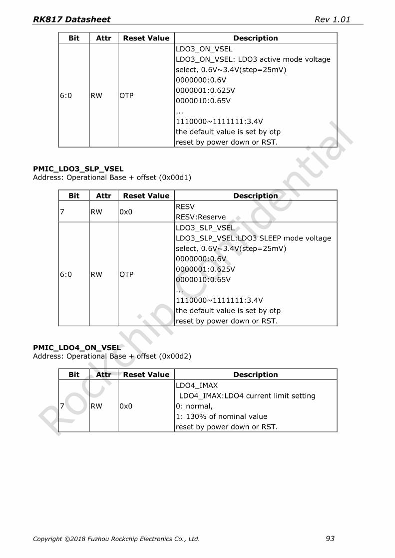
RK817 Datasheet Rev 1.01
Copyright ©2018 Fuzhou Rockchip Electronics Co., Ltd. 93
Bit Attr Reset Value Description
6:0 RW OTP
LDO3_ON_VSEL
LDO3_ON_VSEL: LDO3 active mode voltage
select, 0.6V~3.4V(step=25mV)
0000000:0.6V
0000001:0.625V
0000010:0.65V
...
1110000~1111111:3.4V
the default value is set by otp
reset by power down or RST.
PMIC_LDO3_SLP_VSEL
Address: Operational Base + offset (0x00d1)
Bit Attr Reset Value Description
7 RW 0x0 RESV
RESV:Reserve
6:0 RW OTP
LDO3_SLP_VSEL
LDO3_SLP_VSEL:LDO3 SLEEP mode voltage
select, 0.6V~3.4V(step=25mV)
0000000:0.6V
0000001:0.625V
0000010:0.65V
...
1110000~1111111:3.4V
the default value is set by otp
reset by power down or RST.
PMIC_LDO4_ON_VSEL Address: Operational Base + offset (0x00d2)
Bit Attr Reset Value Description
7 RW 0x0
LDO4_IMAX
LDO4_IMAX:LDO4 current limit setting
0: normal,
1: 130% of nominal value
reset by power down or RST.

RK817 Datasheet Rev 1.01
Copyright ©2018 Fuzhou Rockchip Electronics Co., Ltd. 94
Bit Attr Reset Value Description
6:0 RW OTP
LDO4_ON_VSEL
LDO4_ON_VSEL: LDO4 active mode voltage
select, 0.6V~3.4V(step=25mV)
0000000:0.6V
0000001:0.625V
0000010:0.65V
...
1110000~1111111:3.4V
the default value is set by otp
reset by power down or RST.
PMIC_LDO4_SLP_VSEL
Address: Operational Base + offset (0x00d3)
Bit Attr Reset Value Description
7 RW 0x0 RESV
RESV:Reserve
6:0 RW OTP
LDO4_SLP_VSEL
LDO4_SLP_VSEL:LDO4 SLEEP mode voltage
select, 0.6V~3.4V(step=25mV)
0000000:0.6V
0000001:0.625V
0000010:0.65V
...
1110000~1111111:3.4V
the default value is set by otp
reset by power down or RST.
PMIC_LDO5_ON_VSEL Address: Operational Base + offset (0x00d4)
Bit Attr Reset Value Description
7 RW 0x0
LDO5_IMAX
LDO5_IMAX:LDO5current limit setting
0: normal,
1: 130% of nominal value
reset by power down or RST.

RK817 Datasheet Rev 1.01
Copyright ©2018 Fuzhou Rockchip Electronics Co., Ltd. 95
Bit Attr Reset Value Description
6:0 RW OTP
LDO5_ON_VSEL
LDO5_ON_VSEL: LDO5 active mode voltage
select, 0.6V~3.4V(step=25mV)
0000000:0.6V
0000001:0.625V
0000010:0.65V
...
1110000~1111111:3.4V
the default value is set by otp
reset by power down or RST.
PMIC_LDO5_SLP_VSEL
Address: Operational Base + offset (0x00d5)
Bit Attr Reset Value Description
7 RW 0x0 RESV
RESV:Reserve
6:0 RW OTP
LDO5_SLP_VSEL
LDO5_SLP_VSEL:LDO5 SLEEP mode
voltage select, 0.6V~3.4V(step=25mV)
0000000:0.6V
0000001:0.625V
0000010:0.65V
...
1110000~1111111:3.4V
the default value is set by otp
reset by power down or RST.
PMIC_LDO6_ON_VSEL Address: Operational Base + offset (0x00d6)
Bit Attr Reset Value Description
7 RW 0x0
LDO6_IMAX
LDO6_IMAX:LDO6 current limit setting
0: normal,
1: 130% of nominal value
reset by power down or RST.

RK817 Datasheet Rev 1.01
Copyright ©2018 Fuzhou Rockchip Electronics Co., Ltd. 96
Bit Attr Reset Value Description
6:0 RW OTP
LDO6_ON_VSEL
LDO6_ON_VSEL: LDO6 active mode voltage
select, 0.6V~3.4V(step=25mV)
0000000:0.6V
0000001:0.625V
0000010:0.65V
...
1110000~1111111:3.4V
the default value is set by otp
reset by power down or RST.
PMIC_LDO6_SLP_VSEL
Address: Operational Base + offset (0x00d7)
Bit Attr Reset Value Description
7 RW 0x0 RESV
RESV:Reserve
6:0 RW OTP
LDO6_SLP_VSEL
LDO6_SLP_VSEL:LDO6 SLEEP mode voltage
select, 0.6V~3.4V(step=25mV)
0000000:0.6V
0000001:0.625V
0000010:0.65V
...
1110000~1111111:3.4V
the default value is set by otp
reset by power down or RST.
PMIC_LDO7_ON_VSEL Address: Operational Base + offset (0x00d8)
Bit Attr Reset Value Description
7 RW 0x0
LDO7_IMAX
Field0000 Abstract
LDO7_IMAX:LDO7 current limit setting
0: normal,
1: 130% of nominal value
reset by power down or RST.

RK817 Datasheet Rev 1.01
Copyright ©2018 Fuzhou Rockchip Electronics Co., Ltd. 97
Bit Attr Reset Value Description
6:0 RW OTP
LDO7_ON_VSEL
LDO7_ON_VSEL: LDO7 active mode voltage
select, 0.6V~3.4V(step=25mV)
0000000:0.6V
0000001:0.625V
0000010:0.65V
...
1110000~1111111:3.4V
the default value is set by otp
reset by power down or RST.
PMIC_LDO7_SLP_VSEL
Address: Operational Base + offset (0x00d9)
Bit Attr Reset Value Description
7 RW 0x0 RESV
RESV:Reserve
6:0 RW OTP
LDO7_SLP_VSEL
LDO7_SLP_VSEL:LDO7 SLEEP mode voltage
select, 0.6V~3.4V(step=25mV)
0000000:0.6V
0000001:0.625V
0000010:0.65V
...
1110000~1111111:3.4V
the default value is set by otp
reset by power down or RST.
PMIC_LDO8_ON_VSEL Address: Operational Base + offset (0x00da)
Bit Attr Reset Value Description
7 RW 0x0
LDO8_IMAX
LDO8_IMAX:LDO8 current limit setting
0: normal,
1: 130% of nominal value
reset by power down or RST.

RK817 Datasheet Rev 1.01
Copyright ©2018 Fuzhou Rockchip Electronics Co., Ltd. 98
Bit Attr Reset Value Description
6:0 RW OTP
LDO8_ON_VSEL
Field0000 Abstract
LDO8_ON_VSEL: LDO8 active mode voltage
select, 0.6V~3.4V(step=25mV)
0000000:0.6V
0000001:0.625V
0000010:0.65V
...
1110000~1111111:3.4V
the default value is set by otp
reset by power down or RST.
PMIC_LDO8_SLP_VSEL
Address: Operational Base + offset (0x00db)
Bit Attr Reset Value Description
7 RW 0x0 RESV
RESV:Reserve
6:0 RW OTP
LDO8_SLP_VSEL
LDO8_SLP_VSEL:LDO8 SLEEP mode voltage
select, 0.6V~3.4V(step=25mV)
0000000:0.6V
0000001:0.625V
0000010:0.65V
...
1110000~1111111:3.4V
the default value is set by otp
reset by power down or RST.
PMIC_LDO9_ON_VSEL Address: Operational Base + offset (0x00dc)
Bit Attr Reset Value Description
7 RW 0x0
LDO9_IMAX
LDO9_IMAX:LDO9 current limit setting
0: normal,
1: 130% of nominal value
reset by power down or RST.

RK817 Datasheet Rev 1.01
Copyright ©2018 Fuzhou Rockchip Electronics Co., Ltd. 99
Bit Attr Reset Value Description
6:0 RW OTP
LDO9_ON_VSEL
LDO9_ON_VSEL: LDO9 active mode voltage
select, 0.6V~3.4V(step=25mV)
0000000:0.6V
0000001:0.625V
0000010:0.65V
...
1110000~1111111:3.4V
the default value is set by otp
reset by power down or RST.
PMIC_LDO9_SLP_VSEL
Address: Operational Base + offset (0x00dd)
Bit Attr Reset Value Description
7 RW 0x0 RESV
RESV:Reserve
6:0 RW OTP
LDO9_SLP_VSEL
LDO9_SLP_VSEL:LDO9 SLEEP mode voltage
select, 0.6V~3.4V(step=25mV)
0000000:0.6V
0000001:0.625V
0000010:0.65V
...
1110000~1111111:3.4V
the default value is set by otp
reset by power down or RST.
PMIC_BOOST_OTG_CONFIG0 Address: Operational Base + offset (0x00de)
Bit Attr Reset Value Description
7:6 RW 0x0
OTG_ILIM
OTG_ILIM: OTG current limit selection
00: 1A 01:1.5A 10:1.8A 11: 2.1A
reset by power down or RST.
5 RW 0x0 RESV
Reserved
4:3 RW 0x1
BOOST_ILMAX
BOOST_ILMAX:BOOST inductor peak current
setting
00:2.5A 01:3A 10:4A 11:5A
reset by power down or RST.

RK817 Datasheet Rev 1.01
Copyright ©2018 Fuzhou Rockchip Electronics Co., Ltd. 100
Bit Attr Reset Value Description
2:0 RW OTP
BOOST_ON_VSEL
BOOST_ON_VSEL:BOOST active mode
voltage select.
000:4.7V 001:4.8V 010:4.9V 011:5V
100:5.1V 101:5.2V 110:5.3V 111:5.4V
the default value is set by otp
reset by power down or RST.
PMIC_BOOST_CONFIG1 Address: Operational Base + offset (0x00df)
Bit Attr Reset Value Description
7:5 RW 0x1 RESV
Reserved
4:3 RW 0x2
BOOST_ZCD
BOOST_ZCD<1:0>: BOOSTzero current
detection select
00:50mA 01: 100mA 10:150mA
11:200mA
2:0 RW OTP
BOOST_SLP_VSEL
BOOST_SLP_VSEL:BOOST SLEEP mode
voltage select.
000: 4.7V; 001: 4.8V; 010: 4.9V; 011: 5.0V
100: 5.1V; 101: 5.2V; 110: 5.3V; 111: 5.4V
the default value is set by otp
reset by power down or RST.
PMIC_CHRG_OUT Address: Operational Base + offset (0x00e4)
Bit Attr Reset Value Description
7 RW 0x1
POWERPATH_EN
PWOERPATH_EN: PWOERPATH enable signal
0:disable 1: enable
6:4 RW 0x2
CHRG_VOL_SEL
CHRG_VOL_SEL: charger voltage selection
000:4.1V 001:4.15V 010:4.2V 011:4.25V
100:4.3V 101:4.35; 110:4.4V; 111:4.45V
3 RW 0x0
CHRG_CT_EN
CHRG_CT_EN:Charger Thermal foldback
enable
0:disable 1:enable
2:0 RW 0x2
CHRG_CUR_SEL
CHRG_CUR_SEL: charger current selection
000:1A 001:1.5A 010:2A 011:2.5A
100:2.75A 101:3A 110:3.5A 111:0.5A

RK817 Datasheet Rev 1.01
Copyright ©2018 Fuzhou Rockchip Electronics Co., Ltd. 101
PMIC_CHRG_IN
Address: Operational Base + offset (0x00e5)
Bit Attr Reset Value Description
7 RW 0x1
USB_VLIM_EN
USB_VLIM_EN: whether the USB input
voltage limit function is enable
0:disable 1: enable
6:4 RW 0x4
USB_VLIM_SEL
USB_VLIM_SEL: the USB input voltage limit
selection
000:4.0V 001:4.1V 010:4.2V 011:4.3V
100:4.4V 101:4.5V 110:4.6V 111:4.7V
3 RW 0x1
USB_ILIM_EN
USB_ILIM_EN: whether the USB input
current limit function is enable
0:disable 1: enable
2:0 RW OTP
USB_ILIM_SEL
USB_ILIM_SEL: the USB input average
current limit selection
000:0.45 001:0.08A 010:0.85A 011:1.5A
100:1.75A 101:2A 110:2.5A 111:3A
the default value is set by OTP.
PMIC_CHRG_TERM Address: Operational Base + offset (0x00e6)
Bit Attr Reset Value Description
7 RW 0x1
SYS_CAN_SD
SYS_CAN_SD:whether the system voltage
can be shutdown in Bat_off mode
0:not 1:yes
6 RW 0x1
CHRG_EN
CHRG_EN: enable charger
0:disable 1:enable
reset by power down or RST.
5:4 RW 0x0 RESV
RESV:Reserve
3 RW 0x0
BAT_OVP_EN
BAT_OVP_EN: BAT OVP ENABLE
0:disable 1: enable
2 RW 0x1
CHRG_TERM_ANA_DIG
CHRG_TERM_ANA_DIG:charger termination
adjustment selection
0: analog 1:digital

RK817 Datasheet Rev 1.01
Copyright ©2018 Fuzhou Rockchip Electronics Co., Ltd. 102
Bit Attr Reset Value Description
1:0 RW 0x1
CHRG_TERM_ANA_SEL
CHRG_TERM_ANA_SEL: analog charging
termination selection
00:150mA 01:200mA 10:300mA 11:400mA
PMIC_CHRG_TERM_DIG
Address: Operational Base + offset (0x00e7)
Bit Attr Reset Value Description
7:0 RW 0x20
CHRG_TERM_DIG
CHRG_TERM_DIG: CHRG TERM DIGITAL
CURRENT SELLECT
Compared with BAT_CUR<12:5>
PMIC_BAT_HTS_TS Address: Operational Base + offset (0x00e8)
Bit Attr Reset Value Description
7:0 RW 0x00
BAT_HTS_TS
BAT_HTS_TS: battery high temperature
protection in TS
according to ADC SPEC, high 8bit of ADC
value, the external resistor is negative
temperature coefficient, so
BAT_HTS_TS<BAT_LTS_TS
PMIC_BAT_LTS_TS Address: Operational Base + offset (0x00e9)
Bit Attr Reset Value Description
7:0 RW 0xff
BAT_LTS_TS
BAT_LTS_TS: battery low temperature
protection in TS
according to ADC SPEC,high 8bit of ADC
value, the external resistor is negative
temperature coefficient, so
BAT_HTS_TS<BAT_LTS_TS
PMIC_CHRG_TO Address: Operational Base + offset (0x00ea)

RK817 Datasheet Rev 1.01
Copyright ©2018 Fuzhou Rockchip Electronics Co., Ltd. 103
Bit Attr Reset Value Description
7 RW 0x0
CHRG_TIMER_TRIKL_EN
CHRG_TIMER_TRIKL_EN: trickle charging
timer enable,
0:disable 1:enable
6:4 RW 0x2
CHRG_TIMER_TRIKL
CHRG_TIMER_TRIKL: trickle charge timer
selection
000:30min 001:45min 010:60min
011:90min 100:120min 101:150min
110:180min 111:210min
3 RW 0x0
CHRG_TIMER_CCCV_EN
CHRG_TIMER_CCCV_EN: Constant current
and Constant voltage charging timer enable,
0:disable 1:enable
2:0 RW 0x2
CHRG_TIMER_CCCV
CHRG_TIMER_CCCV:CC CV charge timer
selection
000:4h 001:5h 010:6h 011:8h 100:10h
101:12h 110:14h 111:16h
PMIC_CHRG_STS Address: Operational Base + offset (0x00eb)
Bit Attr Reset Value Description
7 RO 0x0
BAT_EXS
BAT_EXS:bat exists (only writable at test
mode)
0:Not exists 1:exists
6:4 RO 0x0
CHG_STS
CHG_STS: charging status
000: charge off 001:dead charge
010:trickle charge 011: CC or CV charge
100:charge TERM 101:USB over voltage
110:BAT temperature error 111:BAT time
error
3 RO 0x0
BAT_OVP_STS
BAT_OVP_STS:BAT OVP happen, this bit will
be set high.
2 RO 0x0
CHRG_IN_CLAMP
CHRG_IN_CLAMP: When charger incc, incv
or constant temperature happen, this bit will
be set "1"

RK817 Datasheet Rev 1.01
Copyright ©2018 Fuzhou Rockchip Electronics Co., Ltd. 104
Bit Attr Reset Value Description
1 RO 0x0
USB_EXS
USB_EXS:USB exists (only writable at test
mode)
0: Not exists, 1: exists
0 RO 0x0
USB_EFF
USB_EFF:USB is effective (only writable
at test mode)
0: Not effective, 1: effective
PMIC_BAT_DISCHRG
Address: Operational Base + offset (0x00ec)
Bit Attr Reset Value Description
7 RW 0x0 RESV
RESV:Reserve
6 RO 0x0
BAT_DIS_ILIM_STS
BAT_DIS_ILIM_STS:When bat discharge
current is limited, this bit will be set high.
5:4 RW 0x0
BAT_SYS_CMP_DLY
BAT_SYS_CMP_DLY:bat and system
comparator delay time
00:5uS 10:10uS 01:25uS 11:30uS
3 RW 0x1
BAT_DIS_ILIM_EN
BAT_DIS_ILIM_EN:the bat discharger
current limit function enable
0:disable 1:enalbe
2:0 RW 0x2
BAT_DISCHRG_ILIM
BAT_DISCHRG_ILIM:battery discharge
current limit
000:2A 001:2.5A 010:3A 011 3.5A 1xx:4A
PMIC_CHIP_NAME Address: Operational Base + offset (0x00ed)
Bit Attr Reset Value Description
7:0 RO 0x81
CHIP_NAME
CHIP_NAME:CHIP name code<11:4>.
RK817: default 81
PMIC_CHIP_VER
Address: Operational Base + offset (0x00ee)

RK817 Datasheet Rev 1.01
Copyright ©2018 Fuzhou Rockchip Electronics Co., Ltd. 105
Bit Attr Reset Value Description
7:4 RO 0x7
CHIP_NAME
CHIP_NAME:CHIP name code<3:0>.
RK817: default 7
3:0 RO 0x2
CHIP_VER
CHIP_VER:CHIP version code<3:0>, from 1
to 15.
PMIC_OTP_VER
Address: Operational Base + offset (0x00ef)
Bit Attr Reset Value Description
7:6 RW 0x0
LDO1P8A_VSEL
LDO1P8A_VSEL: VCC_1P8A voltage select
00: 1.8V 01: 1.6V 10: 1.9V 11:2.0V
5:4 RO 0x0 RESV
RESV:Reserve
3:0 RO OTP
OTP_VER
OTP_VER: OTP revize version.
default OTP.
PMIC_SYS_STS
Address: Operational Base + offset (0x00f0)
Bit Attr Reset Value Description
7 RO 0x0
PWRON_STS
PWRON_STS: PWRON key status
0: PWRON not press 1:PWRON button
pressed
reset by power down or RST
6 RO 0x0
PLUG_IN_STS
PLUG_IN_STS: USB plug-in event
occurs(USB voltage >3.8V after pull down
20mA current)
0: no USB plug in
1: USB plugged in
5 RO 0x0
VB_UV_STS
VB_UV_STS: Battery under voltage lockout
status
4 RO 0x0
VB_LO_STS
VB_LO_STS: Battery low voltage status
0: VBAT>VB_LO_SEL
1: VBAT<VB_LO_SEL
3 RO 0x0 HOTDIE_STS
HOTDIE_STS: Hot-die warning

RK817 Datasheet Rev 1.01
Copyright ©2018 Fuzhou Rockchip Electronics Co., Ltd. 106
Bit Attr Reset Value Description
2 RO 0x0 TSD_STS
TSD_STS: Thermal shut down
1 RO 0x0
BAT_HI_STS
BAT_HI_STS:battery higher than USB status
bit
0 RO 0x0 SYS_OV_STS
SYS_OV_STS: system over voltage status bit
PMIC_SYS_CFG0 Address: Operational Base + offset (0x00f1)
Bit Attr Reset Value Description
7 RW 0x1
SYS_OV_EN
SYS_OV_EN: SYS over voltage function
enable
0:disable 1:enable
6:4 RW 0x0
VB_UV_SEL
VB_UV_SEL:SYS shut down voltage select,
2.7V~3.4V, step=100mV
000:2.7V; 001:2.8V; 010:2.9V; 011:3.0V
100:3.1V; 101:3.2V; 110:3.3V; 111:3.4V
reset by power down or RST
3 RW 0x1
VB_LO_ACT
VB_LO_ACT: SYS low volatge action
0: shut down system
1: insert interrupt
reset by power down or RST
2:0 RW 0x4
VB_LO_SEL
VB_LO_SEL: SYS low voltage
threshold,2.8V~3.5V, step=100mV
000:2.8V; 001:2.9V; 010:3.0V; 011:3.1V
100:3.2V; 101:3.3V; 110:3.4V; 111:3.5V
reset by power down or RST
PMIC_SYS_CFG1 Address: Operational Base + offset (0x00f2)
Bit Attr Reset Value Description
7 RW 0x1
CLK32KOUT_EN
CLK32KOUT_EN: CLK32K output is enable
1. enable
0. disable
reset by power down or RST
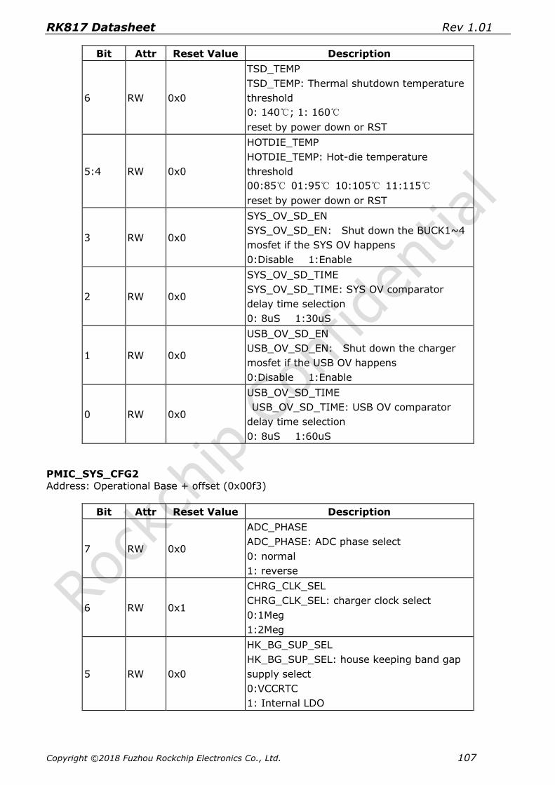
RK817 Datasheet Rev 1.01
Copyright ©2018 Fuzhou Rockchip Electronics Co., Ltd. 107
Bit Attr Reset Value Description
6 RW 0x0
TSD_TEMP
TSD_TEMP: Thermal shutdown temperature
threshold
0: 140; 1: 160
reset by power down or RST
5:4 RW 0x0
HOTDIE_TEMP
HOTDIE_TEMP: Hot-die temperature
threshold
00:85 01:95 10:105 11:115
reset by power down or RST
3 RW 0x0
SYS_OV_SD_EN
SYS_OV_SD_EN: Shut down the BUCK1~4
mosfet if the SYS OV happens
0:Disable 1:Enable
2 RW 0x0
SYS_OV_SD_TIME
SYS_OV_SD_TIME: SYS OV comparator
delay time selection
0: 8uS 1:30uS
1 RW 0x0
USB_OV_SD_EN
USB_OV_SD_EN: Shut down the charger
mosfet if the USB OV happens
0:Disable 1:Enable
0 RW 0x0
USB_OV_SD_TIME
USB_OV_SD_TIME: USB OV comparator
delay time selection
0: 8uS 1:60uS
PMIC_SYS_CFG2
Address: Operational Base + offset (0x00f3)
Bit Attr Reset Value Description
7 RW 0x0
ADC_PHASE
ADC_PHASE: ADC phase select
0: normal
1: reverse
6 RW 0x1
CHRG_CLK_SEL
CHRG_CLK_SEL: charger clock select
0:1Meg
1:2Meg
5 RW 0x0
HK_BG_SUP_SEL
HK_BG_SUP_SEL: house keeping band gap
supply select
0:VCCRTC
1: Internal LDO

RK817 Datasheet Rev 1.01
Copyright ©2018 Fuzhou Rockchip Electronics Co., Ltd. 108
Bit Attr Reset Value Description
4 RW 0x0
HK_REF_RES_SEL
HK_REF_RES_SEL: house keeping reference
filter resistor select
0:100%
1:200%
3 RW 0x0
HK_REF_LP_EN
HK_REF_LP_EN: house keeping reference
lower power enable
1. enable
0. disable
2 RW 0x0
USB_OV_SEL
USB_OV_SEL: usb over voltage threshold
select
0: 6V
1: 5.8V
1 RW 0x0
SYS_UV_PRE_DLY
SYS_UV_PRE_DLY: SYS under voltage delay
time select
0:1.5uS
1:5uS
0 RW 0x0
USB_OV_DLY
USB_OV_DLY: usb over voltage delay time
select
0: 5uS
1:3uS
PMIC_SYS_CFG3 Address: Operational Base + offset (0x00f4)
Bit Attr Reset Value Description
7:6 RW 0x0
RST_FUN: reset function selection:
00: Restart the PMU.
01: reset DCDC and LDO. (Do not use this
mode when SLEEP.)
1x: Do not use.
5 RW 0x1
SLP_POL
SLP_POL: SLEEP pin polarity
0:active low
1:active high
reset by power down or RST

RK817 Datasheet Rev 1.01
Copyright ©2018 Fuzhou Rockchip Electronics Co., Ltd. 109
Bit Attr Reset Value Description
4:3 RW 0x0
SLP_FUN
SLP_FUN: SLEEP PIN function selection:
00: not effect; 01: sleep function;
10:shutdown function; 11:restart pmu
function.
reset by power down or RST
2 RW 0x0
DEV_RST
DEV_RST: Write 1 will 'RST' the device.
Note: 'RST' is not only a reset source, but a
special function defined by 'RST_FUN'
reset by power down or RST
1 RW 0x0
DEV_SLP
DEV_SLP: Write 1 will go to SLEEP state.
reset by power down or RST
0 RW 0x0
DEV_OFF
DEV_OFF: Write 1 will shutdown the device.
reset by power down or RST
PMIC_ON_SOURCE Address: Operational Base + offset (0x00f5)
Bit Attr Reset Value Description
7 RO 0x0
ON_PWRON
ON_PWRON: PRESS PWRON to turn on PMU
reset by power down or RST, and load this
bit after reset.
6 RO 0x0
ON_PLUG_IN
ON_PLUG_IN:USB PLUG IN to turn on PMU
reset by power down or RST
5 RO 0x0
ON_RTC
ON_RTC:RTC timer to turn on PMU
reset by power down or RST
4 RO 0x0
RESTART_RESETB
RESTART_RESETB:PULL LOW the RESETB
PIN to restart the PMU
reset by power down or RST
3 RO 0x0
RESTART_PWRON_LP
RESTART_PWRON_LP:Long press PWRON to
restart the PMU
reset by power down or RST
2 RO 0x0
RESTART_SLP
RESTART_SLP:SLEEP PIN ACTIVE to restart
the PMU
reset by power down or RST

RK817 Datasheet Rev 1.01
Copyright ©2018 Fuzhou Rockchip Electronics Co., Ltd. 110
Bit Attr Reset Value Description
1 RW 0x0
RESTART_DEV_RST
RESTART_DEV_RST: I2C write DEV_RST to
restart PMU
reset by power down or RST
0 RO 0x0 RESV
RESV: Reserve
PMIC_OFF_SOURCE
Address: Operational Base + offset (0x00f6)
Bit Attr Reset Value Description
7 RO 0x0
OFF_SLP
OFF_SLP: SLEEP PIN ACTIVE to turn off PMU
reset by power down or RST, and load this
bit after reset.
6 RO 0x0
OFF_SYS_OV
OFF_SYS_OV:SYS OV to turn off PMU
reset by power down or RST, and load this
bit after reset.
5 RO 0x0
OFF_TSD
OFF_TSD:TSD to turn off PMU
reset by power down or RST, and load this
bit after reset.
4 RO 0x0
OFF_VB_UV
OFF_VB_UV:SYS UV to turn off PMU
reset by power down or RST, and load this
bit after reset.
3 RO 0x0
OFF_DEV_OFF
OFF_DEV_OFF:I2C write DEV_OFF to turn off
PMU
reset by power down or RST, and load this
bit after reset.
2 RO 0x0
OFF_PWRON_LP
OFF_PWRON_LP:long press PWRON to turn
off PMU
reset by power down or RST, and load this
bit after reset.
1 RO 0x0
OFF_USB_EFF_NOT
OFF_USB_EFF_NOT: USB OV or UV to turn
off PMU when BUCK MODE
reset by power down or RST, and load this
bit after reset.

RK817 Datasheet Rev 1.01
Copyright ©2018 Fuzhou Rockchip Electronics Co., Ltd. 111
Bit Attr Reset Value Description
0 RO 0x0
OFF_VB_LO
OFF_VB_LO:SYS Low (if VB_LO_ACT=0)to
turn off PMU
reset by power down or RST, and load this
bit after reset.
PMIC_PWRON_KEY
Address: Operational Base + offset (0x00f7)
Bit Attr Reset Value Description
7 RW OTP
PWRON_ON_TIME
PWRON_ON_TIME:0:500mS; 1:100mS
default OTP.
6 RW 0x0
PWRON_LP_ACT
PWRON_LP_ACT: PWRON long press act
0: turn off
1: turn off and then restart
5:4 RW 0x0
PWRON_LP_OFF_TIME
PWRON_LP_OFF_TIME: PWRON long press
time:
00: 6s, 01: 8s, 10: 10s, 11: 12s
3:2 RW 0x1
PWRON_LP_TM
PWRON_LP_TM_SEL<1:0>:PWRON long
press interrupt time selection:
00: 0.5S 01:1S 10:1.5S 11:2S
1:0 RW 0x2
PWRON_DB_SEL
PWRON_DB_SEL<1:0>:PWRON interrupt
debounce time selection:
00: 32uS 01:10mS 10:20mS 11:40mS
PMIC_INT_STS0 Address: Operational Base + offset (0x00f8)
Bit Attr Reset Value Description
7 W1C 0x0
VB_LO_INT
VB_LO_INT: Battery under voltage alarm
event interrupt status.
reset by power down or RST.
6 W1C 0x0
RTC_PERIOD_INT
RTC_PERIOD_INT: RTC period event
interrupt.
reset by power down or RST.
5 W1C 0x0
RTC_ALARM_INT
RTC_ALARM_INT: RTC alarm event interrupt.
reset by power down or RST.

RK817 Datasheet Rev 1.01
Copyright ©2018 Fuzhou Rockchip Electronics Co., Ltd. 112
Bit Attr Reset Value Description
4 W1C 0x0
HOTDIE_INT
HOTDIE_INT: Hot die event interrupt
status.
reset by power down or RST.
3 W1C 0x0
PWRON_LP_INT
PWRON_LP_INT: PWRON PIN long press
event interrupt status.
reset by power down or RST.
2 W1C 0x0
PWRON_INT
PWRON_INT: PWRON event interrupt
status.
reset by power down or RST.
1 W1C 0x0
PWRON_RISE_INT
PWRON_RISE_INT:PWRON rising event
interrupt
reset by power down or RST.
0 W1C 0x0
PWRON_FALL_INT
PWRON_FALL_INT:PWRON falling event
interrupt
reset by power down or RST.
PMIC_INT_MSK0 Address: Operational Base + offset (0x00f9)
Bit Attr Reset Value Description
7 RW 0x0
VB_LO_IM
VB_LO_IM: Battery under voltage alarm
event interrupt mask
reset by power down or RST.
6 RW 0x0
RTC_PERIOD_IM
RTC_PERIOD_IM: RTC period event interrupt
mask
reset by power down or RST.
5 RW 0x0
RTC_ALARM_IM
RTC_ALARM_IM: RTC alarm event interrupt
mask
reset by power down or RST.
4 RW 0x0
HOTDIE_IM
HOTDIE_IM: Hot die event interrupt mask
reset by power down or RST.
3 RW 0x0
PWRON_LP_IM
PWRON_LP_IM: PWRON PIN long press
event interrupt mask
reset by power down or RST.

RK817 Datasheet Rev 1.01
Copyright ©2018 Fuzhou Rockchip Electronics Co., Ltd. 113
Bit Attr Reset Value Description
2 RW 0x0
PWRON_IM
PWRON_IM:PWRON event interrupt mask
reset by power down or RST.
1 RW 0x0
PWRON_RISE_INT_IM
PWRON_RISE_INT_IM:PWRON rising event
interrupt mask
reset by power down or RST.
0 RW 0x0
PWRON_FALL_INT_IM
PWRON_FALL_INT_IM:PWRON falling event
interrupt mask
reset by power down or RST.
PMIC_INT_STS1 Address: Operational Base + offset (0x00fa)
Bit Attr Reset Value Description
7 W1C 0x0
BAT_DIS_ILIM_INT
BAT_DIS_ILIM_INT:Battery discharge
current over the setting value event
interrupt.
reset by power down or RST.
6 W1C 0x0
CHRG_IN_CLMP_INT
CHRG_IN_CLMP_INT:Charger USB input
current limit or USB input voltage limit or
chip constant temperature event interrupt
(write 1 clear or POWERPATH_EN=0 clear)
5 W1C 0x0
USB_OV_INT
USB_OV_INT:USB over voltage event
interrupt
(write 1 clear or POWERPATH_EN=0 clear)
4 W1C 0x0
CHRG_TS_INT
CHRG_TS_INT:Charger TS over or under
temperature event interrupt
(write 1 clear or POWERPATH_EN=0 clear)
3 W1C 0x0
CHRG_TIME_INT
CHRG_TIME_INT:Charger time error event
interrupt
(write 1 clear or POWERPATH_EN=0 clear)
2 W1C 0x0
CHRG_TERM__INT
CHRG_TERM__INT:Charger finished event
interrupt
(write 1 clear or POWERPATH_EN=0 clear)
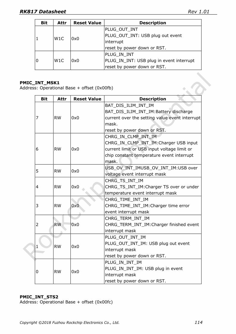
RK817 Datasheet Rev 1.01
Copyright ©2018 Fuzhou Rockchip Electronics Co., Ltd. 114
Bit Attr Reset Value Description
1 W1C 0x0
PLUG_OUT_INT
PLUG_OUT_INT: USB plug out event
interrupt
reset by power down or RST.
0 W1C 0x0
PLUG_IN_INT
PLUG_IN_INT: USB plug in event interrupt
reset by power down or RST.
PMIC_INT_MSK1
Address: Operational Base + offset (0x00fb)
Bit Attr Reset Value Description
7 RW 0x0
BAT_DIS_ILIM_INT_IM
BAT_DIS_ILIM_INT_IM:Battery discharge
current over the setting value event interrupt
mask.
reset by power down or RST.
6 RW 0x0
CHRG_IN_CLMP_INT_IM
CHRG_IN_CLMP_INT_IM:Charger USB input
current limit or USB input voltage limit or
chip constant temperature event interrupt
mask.
5 RW 0x0 USB_OV_INT_IMUSB_OV_INT_IM:USB over
voltage event interrupt mask
4 RW 0x0
CHRG_TS_INT_IM
CHRG_TS_INT_IM:Charger TS over or under
temperature event interrupt mask
3 RW 0x0
CHRG_TIME_INT_IM
CHRG_TIME_INT_IM:Charger time error
event interrupt mask
2 RW 0x0
CHRG_TERM_INT_IM
CHRG_TERM_INT_IM:Charger finished event
interrupt mask
1 RW 0x0
PLUG_OUT_INT_IM
PLUG_OUT_INT_IM: USB plug out event
interrupt mask
reset by power down or RST.
0 RW 0x0
PLUG_IN_INT_IM
PLUG_IN_INT_IM: USB plug in event
interrupt mask
reset by power down or RST.
PMIC_INT_STS2 Address: Operational Base + offset (0x00fc)

RK817 Datasheet Rev 1.01
Copyright ©2018 Fuzhou Rockchip Electronics Co., Ltd. 115
Bit Attr Reset Value Description
7 RC 0x0
CHRG_BAT_HI_INT
CHRG_BAT_HI_INT: BAT HI interrupt.
reset by power down or RST.
6 W1C 0x0
BAT_OVP_INT
BAT_OVP_INT:BAT OVP interrupt.
reset by power down or RST.
5 W1C 0x0
CLASSD_OCP_INT
CLASSD_OCP_INT:CLASS D OCP interrupt.
reset by power down or RST.
4 W1C 0x0
CLASSD_MUTE_DONE
CLASSD_MUTE_DONE_INT:CLASSD_MUTE_D
ONE interrupt.
reset by power down or RST.
3 W1C 0x0
CODEC_PO_INT
CODEC_PO_INT: CODEC ANTI-POP DAC
SMART POWER ON DONE interrupt.
reset by power down or RST.
2 W1C 0x0
CODEC_PD_INT
CODEC_PD_INT: CODEC ANTI-POP DAC
SMART POWER OFF DONE interrupt.
reset by power down or RST.
1 W1C 0x0
TS_GPIO_INT
TS_GPIO_INT: TS_GPIO PIN input signal
posedge or negedge interrupt.
reset by power down or RST.
0 W1C 0x0
GATE_GPIO_INT
GATE_GPIO_INT: GATE_GPIO PIN input
signal posedge or negedge interrupt.
reset by power down or RST.
PMIC_INT_MSK2 Address: Operational Base + offset (0x00fd)
Bit Attr Reset Value Description
7 RW 0x0
CHRG_BAT_HI_INT_IM
CHRG_BAT_HI_INT_IM:BAT HI interrupt
mask.
reset by power down or RST.
6 RW 0x0
BAT_OVP_INT_IM
BAT_OVP_INT_IM:BAT OVP interrupt mask.
reset by power down or RST.
5 RW 0x0
CLASSD_OCP_INT_IM
CLASSD_OCP_INT_IM:CLASS D OCP
interrupt mask.
reset by power down or RST.
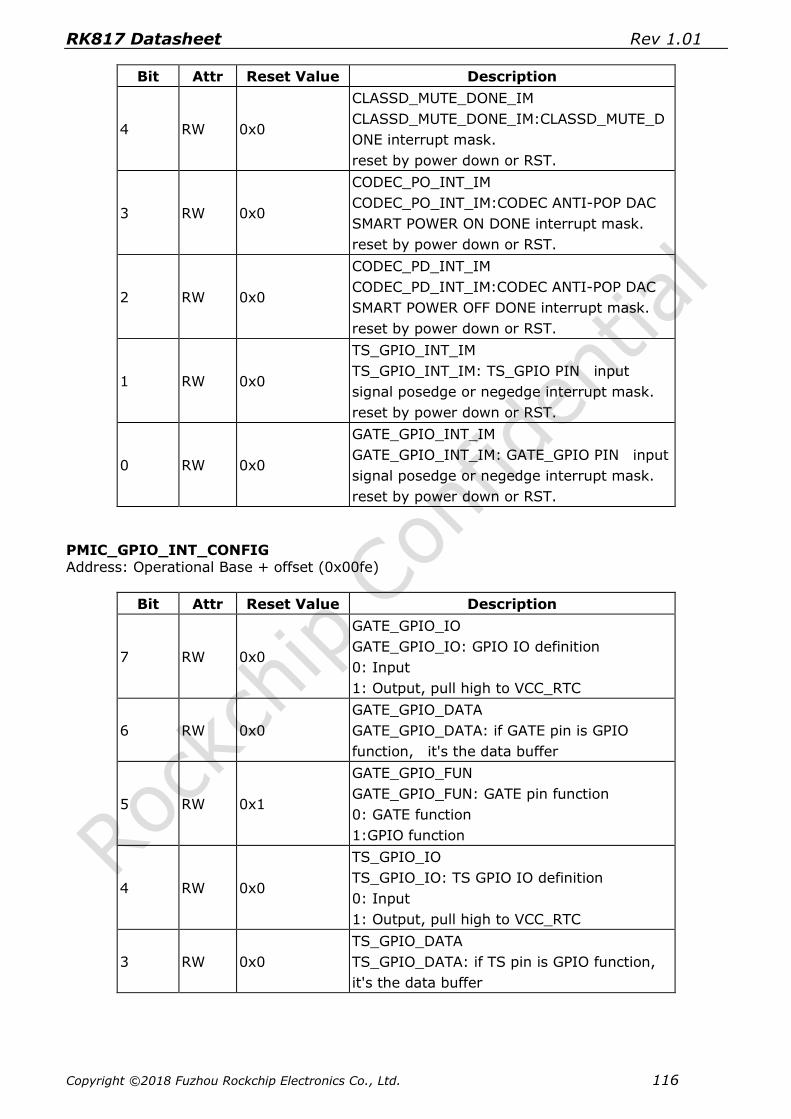
RK817 Datasheet Rev 1.01
Copyright ©2018 Fuzhou Rockchip Electronics Co., Ltd. 116
Bit Attr Reset Value Description
4 RW 0x0
CLASSD_MUTE_DONE_IM
CLASSD_MUTE_DONE_IM:CLASSD_MUTE_D
ONE interrupt mask.
reset by power down or RST.
3 RW 0x0
CODEC_PO_INT_IM
CODEC_PO_INT_IM:CODEC ANTI-POP DAC
SMART POWER ON DONE interrupt mask.
reset by power down or RST.
2 RW 0x0
CODEC_PD_INT_IM
CODEC_PD_INT_IM:CODEC ANTI-POP DAC
SMART POWER OFF DONE interrupt mask.
reset by power down or RST.
1 RW 0x0
TS_GPIO_INT_IM
TS_GPIO_INT_IM: TS_GPIO PIN input
signal posedge or negedge interrupt mask.
reset by power down or RST.
0 RW 0x0
GATE_GPIO_INT_IM
GATE_GPIO_INT_IM: GATE_GPIO PIN input
signal posedge or negedge interrupt mask.
reset by power down or RST.
PMIC_GPIO_INT_CONFIG Address: Operational Base + offset (0x00fe)
Bit Attr Reset Value Description
7 RW 0x0
GATE_GPIO_IO
GATE_GPIO_IO: GPIO IO definition
0: Input
1: Output, pull high to VCC_RTC
6 RW 0x0
GATE_GPIO_DATA
GATE_GPIO_DATA: if GATE pin is GPIO
function, it's the data buffer
5 RW 0x1
GATE_GPIO_FUN
GATE_GPIO_FUN: GATE pin function
0: GATE function
1:GPIO function
4 RW 0x0
TS_GPIO_IO
TS_GPIO_IO: TS GPIO IO definition
0: Input
1: Output, pull high to VCC_RTC
3 RW 0x0
TS_GPIO_DATA
TS_GPIO_DATA: if TS pin is GPIO function,
it's the data buffer

RK817 Datasheet Rev 1.01
Copyright ©2018 Fuzhou Rockchip Electronics Co., Ltd. 117
Bit Attr Reset Value Description
2 RW 0x0
TS_GPIO_FUN
TS_GPIO_FUN: TS pin function
0: TS function
1:GPIO function
1 RW 0x1
INT_POL
INT_POL: INT pin polarity
0: active low
1: active high
reset by power down or RST.
0 RW 0x0
INT_FC_EN
INT_FC_EN:interrupt watchdog function
enable
0:disable
1:enable
reset by power down or RST.

RK817 Datasheet Rev 1.01
Copyright ©2018 Fuzhou Rockchip Electronics Co., Ltd. 118
Chapter 6 Thermal Management
6.1 Overview
For reliability and operability concerns, the absolute maximum junction temperature of RK817 has to be below 125ºC.
Depending on the thermal mechanical design (Smartphone, Tablet, Personal Navigation
Device, etc), the system thermal management software and worst case thermal applications, the junction temperature might be exposed to higher values than those specified above.
Therefore, it is recommended to perform thermal simulations at device level (Smartphone,
Tablet, Personal Navigation Device, etc) with the measured power of the worst case UC of the device.
6.2 Package Thermal Characteristics
Table 6-1 provides the thermal resistance characteristics for the package used on this
device.
Table 6-1 Thermal Resistance Characteristics
PACKAGE
(QFN7X7-68) POWER(W) 𝜽𝑱𝑨(/𝑾) 𝜽𝑱𝑩(/𝑾) 𝜽𝑱𝑪(/𝑾)
RK817 2 21.99 12 6.58
Note: The testing PCB is based on 4 layers, 114mm x 76 mm, 1.6mm thickness, Ambient temperature is 85°C.