

Robust Low Power VLSI R obust L ow P ower VLSI Tutorial to Correct Unwanted Silk Screen Overlaps in...
14
Robu st Low Powe r VLSI Robust Low Power VLSI Tutorial to Correct Unwanted Silk Screen Overlaps in the Final PCB Arijit Banerjee
-
Upload
joel-stafford -
Category
Documents
-
view
215 -
download
0
Transcript of Robust Low Power VLSI R obust L ow P ower VLSI Tutorial to Correct Unwanted Silk Screen Overlaps in...

Rob
ust
Low
Power
VLSI
Robust
LowPower
VLSI
Tutorial to Correct Unwanted Silk Screen Overlaps in the Final PCB
Arijit Banerjee

Rob
ust
Low
Power
VLSI 2
The IssueWhen you see the routed layout it looks OK After you submit in the Advanced Circuit and have the “results” email, if you look into the PDF attached full Layout view you may see some unwanted Silk Screen texts are overlapping with your documentation

Rob
ust
Low
Power
VLSI 3
Snapshot of No-Silk-Screen-Issue in Routed Layout

Rob
ust
Low
Power
VLSI 4
Snapshot of Silk-Screen-Issue in the “Results” Pdf from Advanced Circuit
Rob
ust
Low
Power
VLSI 5
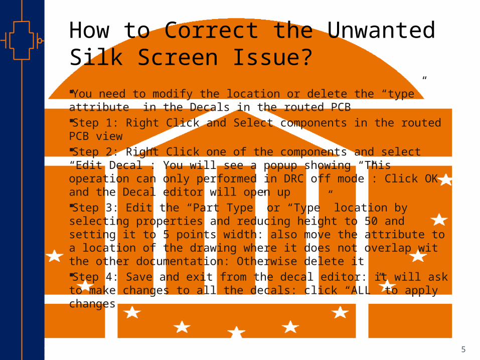
How to Correct the Unwanted Silk Screen Issue?You need to modify the location or delete the “type” attribute in the Decals in the routed PCBStep 1: Right Click and Select components in the routed PCB viewStep 2: Right Click one of the components and select “Edit Decal”: You will see a popup showing “This operation can only performed in DRC off mode”: Click OK and the Decal editor will open upStep 3: Edit the “Part Type” or “Type” location by selecting properties and reducing height to 50 and setting it to 5 points width: also move the attribute to a location of the drawing where it does not overlap wit the other documentation: Otherwise delete itStep 4: Save and exit from the decal editor: it will ask to make changes to all the decals: click “ALL” to apply changes

Rob
ust
Low
Power
VLSI 6
Screenshot of Step 1
Rob
ust
Low
Power
VLSI 7
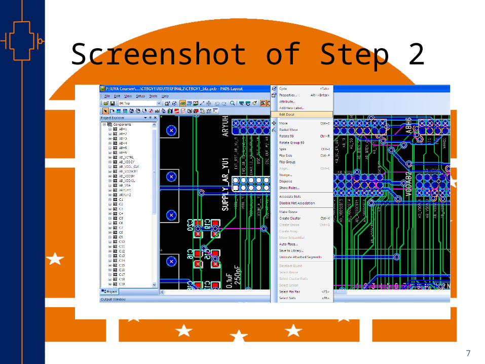
Screenshot of Step 2

Rob
ust
Low
Power
VLSI 8
Screenshot of Step 2 contd.

Rob
ust
Low
Power
VLSI 9
Screenshot of Step 3

Rob
ust
Low
Power
VLSI 10
Screenshot of Step 3 contd.
Rob
ust
Low
Power
VLSI 11
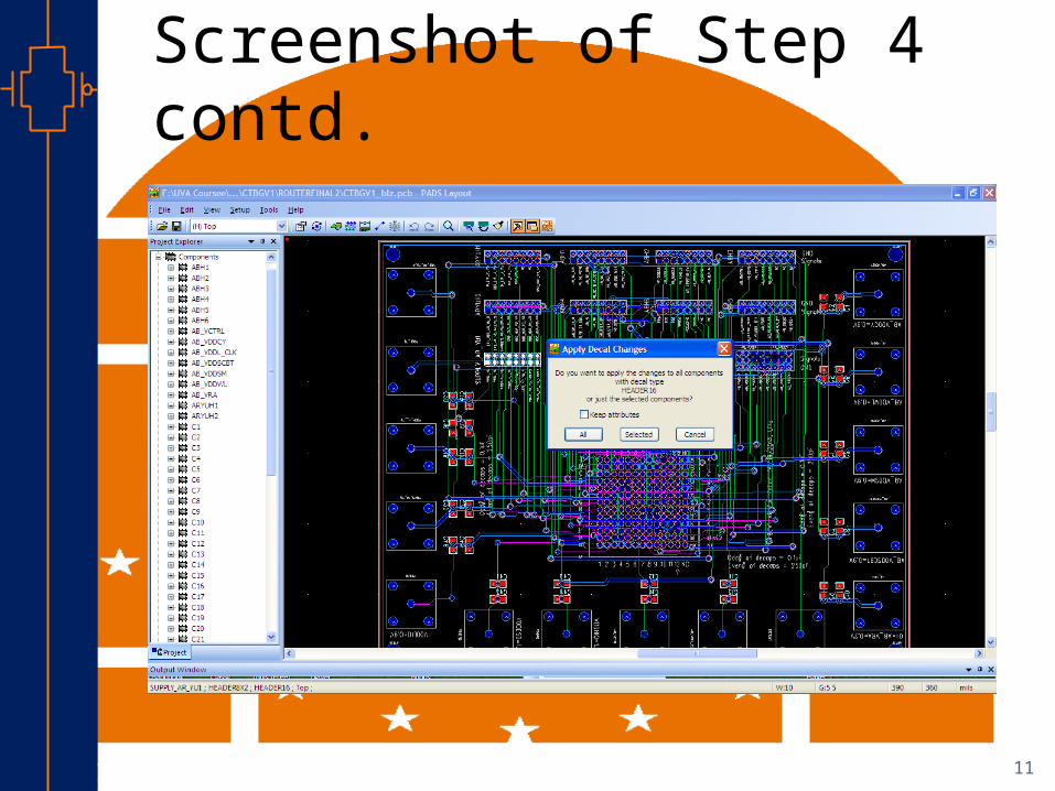
Screenshot of Step 4 contd.
Rob
ust
Low
Power
VLSI 12
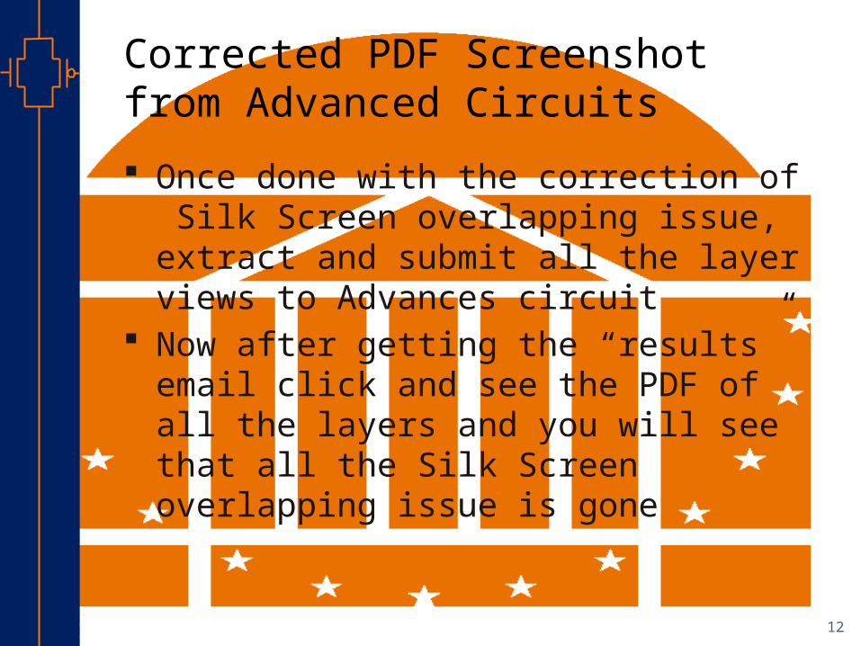
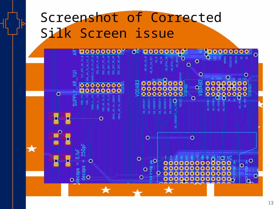
Corrected PDF Screenshot from Advanced Circuits Once done with the correction of Silk Screen
overlapping issue, extract and submit all the layer views to Advances circuit
Now after getting the “results” email click and see the PDF of all the layers and you will see that all the Silk Screen overlapping issue is gone
Rob
ust
Low
Power
VLSI 13
Screenshot of Corrected Silk Screen issue