RLDRAM II Controller MegaCore Function v9.1 User … · OpenCore Plus Evaluation ... functional...
62
101 Innovation Drive San Jose, CA 95134 www.altera.com RLDRAM II Controller MegaCore Function User Guide MegaCore Version: 9.1 Document Date: November 2009 CAUTION: The IP described in this document is scheduled for product obsolescence and discontinued support as described in PDN1403. Therefore, Altera does not recommend use of this IP in new designs. For more information about Altera's current IP offering, refer to Altera's Intellectual Property website.
Transcript of RLDRAM II Controller MegaCore Function v9.1 User … · OpenCore Plus Evaluation ... functional...

101 Innovation DriveSan Jose, CA 95134www.altera.com
RLDRAM II Controller
MegaCore Function User Guide
MegaCore Version: 9.1Document Date: November 2009
CAUTION: The IP described in this document is scheduled for product obsolescenceand discontinued support as described in PDN1403. Therefore, Altera does notrecommend use of this IP in new designs. For more information about Altera'scurrent IP offering, refer to Altera's Intellectual Property website.

Copyright © 2009 Altera Corporation. All rights reserved. Altera, The Programmable Solutions Company, the stylized Altera logo, specific device des-ignations, and all other words and logos that are identified as trademarks and/or service marks are, unless noted otherwise, the trademarks andservice marks of Altera Corporation in the U.S. and other countries. All other product or service names are the property of their respective holders. Al-tera products are protected under numerous U.S. and foreign patents and pending applications, maskwork rights, and copyrights. Altera warrantsperformance of its semiconductor products to current specifications in accordance with Altera's standard warranty, but reserves the right to makechanges to any products and services at any time without notice. Altera assumes no responsibility or liability arising out of the ap-plication or use of any information, product, or service described herein except as expressly agreed to in writing by AlteraCorporation. Altera customers are advised to obtain the latest version of device specifications before relying on any published in-formation and before placing orders for products or services.
ii MegaCore Version 9.1 Altera CorporationRLDRAM II Controller MegaCore Function User Guide
UG-RLDRAM-8.1
Altera Corporation M
Contents
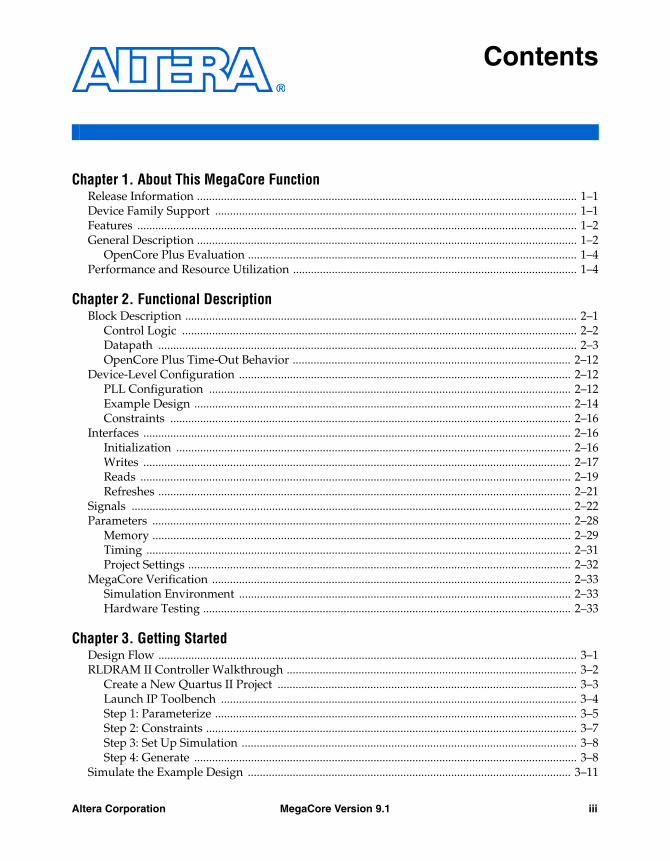
Chapter 1. About This MegaCore FunctionRelease Information ............................................................................................................................... 1–1Device Family Support ......................................................................................................................... 1–1Features ................................................................................................................................................... 1–2General Description ............................................................................................................................... 1–2
OpenCore Plus Evaluation .............................................................................................................. 1–4Performance and Resource Utilization ............................................................................................... 1–4
Chapter 2. Functional DescriptionBlock Description ................................................................................................................................... 2–1
Control Logic .................................................................................................................................... 2–2Datapath ............................................................................................................................................ 2–3OpenCore Plus Time-Out Behavior ............................................................................................. 2–12
Device-Level Configuration ............................................................................................................... 2–12PLL Configuration ......................................................................................................................... 2–12Example Design .............................................................................................................................. 2–14Constraints ...................................................................................................................................... 2–16
Interfaces ............................................................................................................................................... 2–16Initialization .................................................................................................................................... 2–16Writes ............................................................................................................................................... 2–17Reads ................................................................................................................................................ 2–19Refreshes .......................................................................................................................................... 2–21
Signals ................................................................................................................................................... 2–22Parameters ............................................................................................................................................ 2–28
Memory ............................................................................................................................................ 2–29Timing .............................................................................................................................................. 2–31Project Settings ................................................................................................................................ 2–32
MegaCore Verification ........................................................................................................................ 2–33Simulation Environment ............................................................................................................... 2–33Hardware Testing ........................................................................................................................... 2–33
Chapter 3. Getting StartedDesign Flow ............................................................................................................................................ 3–1RLDRAM II Controller Walkthrough ................................................................................................. 3–2
Create a New Quartus II Project .................................................................................................... 3–3Launch IP Toolbench ....................................................................................................................... 3–4Step 1: Parameterize ......................................................................................................................... 3–5Step 2: Constraints ............................................................................................................................ 3–7Step 3: Set Up Simulation ................................................................................................................ 3–8Step 4: Generate ................................................................................................................................ 3–8
Simulate the Example Design ............................................................................................................ 3–11
egaCore Version 9.1 iii

Contents
Simulate with IP Functional Simulation Models ....................................................................... 3–11Simulating in Third-Party Simulation Tools Using NativeLink ............................................. 3–12
Edit the PLL .......................................................................................................................................... 3–13Compile the Example Design ............................................................................................................ 3–14Program a Device ................................................................................................................................ 3–15Implement Your Design ..................................................................................................................... 3–15Set Up Licensing .................................................................................................................................. 3–15
Additional InformationRevision History ......................................................................................................................................... iHow to Contact Altera ............................................................................................................................... iTypographic Conventions ....................................................................................................................... ii
iv MegaCore Version 9.1 Altera CorporationRLDRAM II Controller MegaCore Function User Guide

Altera Corporation MNovember 2009
1. About This MegaCoreFunction
Release Information
Table 1–1 provides information about this release of the Altera® RLDRAM II Controller MegaCore® function.
f For more information about this release, refer to the MegaCore IP Library Release Notes and Errata.
Altera verifies that the current version of the Quartus® II software compiles the previous version of each MegaCore function. The MegaCore IP Library Release Notes and Errata report any exceptions to this verification. Altera does not verify compilation with MegaCore function versions older than one release.
Device Family Support
MegaCore functions provide either full or preliminary support for target Altera device families:
■ Full support means the MegaCore function meets all functional and timing requirements for the device family and may be used in production designs
■ Preliminary support means the MegaCore function meets all functional requirements, but may still be undergoing timing analysis for the device family; it may be used in production designs with caution.
Table 1–1. Release Information
Item Description
Version 9.1
Release Date November 2009
Ordering Code IP-RLDRAMII
Product ID 00AC
Vendor ID 6AF7
egaCore Version 9.1 1–1

Features
Table 1–2 shows the level of support offered by the RLDRAM II Controller MegaCore function to each Altera device family.
Features ■ Common I/O (CIO) and separate I/O (SIO) device support■ Memory burst length 2, 4, and 8-beat support■ Nonmultiplexed addressing■ Datapath generation ■ Data strobe signal (DQS) and non-DQS capture modes■ Automatic constraint generation■ Easy-to-use IP Toolbench interface■ IP functional simulation models for use in Altera-supported VHDL
and Verilog HDL simulators■ Support for OpenCore Plus evaluation
General Description
The RLDRAM II controller MegaCore function handles the complex aspects of using RLDRAM II—initializing the memory devices and translating read and write requests from the local interface into all the necessary RLDRAM II command signals.
The RLDRAM II controller is optimized for Altera Stratix II devices and has preliminary support for Stratix II GX and HardCopy II devices. The advanced features available in these devices allow you to interface directly to RLDRAM II devices.
Figure 1–1 on page 1–3 shows a system-level diagram including the example design that the RLDRAM II Controller MegaCore function creates for you.
Table 1–2. Device Family Support
Device Family Support
HardCopy® II Preliminary
Stratix® II Full
Stratix II GX Full
Other device families No support
1–2 MegaCore Version 9.1 Altera CorporationRLDRAM II Controller MegaCore Function User Guide November 2009

About This MegaCore Function
Figure 1–1. RLDRAM II Controller System-Level Diagram
Note to Figure 1–1:(1) Non-DQS mode only.
IP Toolbench generates the following items:
■ A testbench, which instantiates the example design■ A synthesizable example design which instantiates the following
modules:● RLDRAM II controller:
• Encrypted control logic, which takes transaction requests from the local interface and issues writes, reads, and refreshes to the memory interface
• A clear-text datapath● Example driver—generates write, read and refresh requests and
outputs a pass_fail signal to indicate that the tests are passing or failing
● System phase-locked loop (PLL)—generates the RLDRAM II controller clocks
● Delay locked loop (DLL)—instantiated in DQS mode and generates the DQS delay control signal for the dedicated DQS delay circuitry
RLDRAM II
Example Driver
SystemPLL
DLL
RLDRAM IIInterface
Passor Fail
Clock
Local Interface
Example Design
RLDRAM II Controller
Datapath(Clear Text)
Control Logic(Encrypted)
FedbackClock
PLL (1)
Altera Corporation MegaCore Version 9.1 1–3November 2009 RLDRAM II Controller MegaCore Function User Guide

Performance and Resource Utilization
● Optional fedback clock PLL—instantiated in non-DQS mode and generates a capture clock for the datapath read capture and logic path
OpenCore Plus Evaluation
With Altera’s free OpenCore Plus evaluation feature, you can perform the following actions:
■ Simulate the behavior of a megafunction (Altera MegaCore function or AMPPSM megafunction) within your system
■ Verify the functionality of your design, as well as evaluate its size and speed quickly and easily
■ Generate time-limited device programming files for designs that include MegaCore functions
■ Program a device and verify your design in hardware
You only need to obtain a license for the megafunction when you are completely satisfied with its functionality and performance, and want to take your design to production.
f For more information on OpenCore Plus hardware evaluation using the RLDRAM II controller, refer to “OpenCore Plus Time-Out Behavior” on page 2–12 and AN 320: OpenCore Plus Evaluation of Megafunctions.
Performance and Resource Utilization
Table 1–3 shows typical expected performance for the RLDRAM II Controller MegaCore function, with the Quartus II software.
Table 1–3. Performance
Device Capture Mode fMAX (MHz)
Stratix II (EP2S60F1020C3)
Non-DQS 200
DQS 300
Stratix II GX (EP2SGX30CF780C3)
Non-DQS 200
DQS 300
1–4 MegaCore Version 9.1 Altera CorporationRLDRAM II Controller MegaCore Function User Guide November 2009

About This MegaCore Function
Stratix II and Stratix II GX devices support RLDRAM at up to 300 MHz. Table 1–4 shows the clock frequency support for Stratix II and Stratix GX device families, with the Quartus II software.
Table 1–5 shows typical sizes in combinational adaptive look-up tables (ALUTs) and logic registers for the RLDRAM II controller.
Table 1–4. RLDRAM II Maximum Clock Frequency Support in Stratix II & Stratix GX Devices
Speed Grade Frequency (MHz)
–3 300
–4 250
–5 200
Table 1–5. Typical Size Note (1)
Device Memory Width (Bits) CombinationalALUTs
Logic Registers
Stratix II and Stratix II GX
9 127 169
18 130 209
36 151 287
72 185 444
Notes to Table 1–5:(1) These sizes are a guide only and vary with different choices of parameters.
Altera Corporation MegaCore Version 9.1 1–5November 2009 RLDRAM II Controller MegaCore Function User Guide

Performance and Resource Utilization
1–6 MegaCore Version 9.1 Altera CorporationRLDRAM II Controller MegaCore Function User Guide November 2009

Altera Corporation MNovember 2009
2. Functional Description
Block Description
Figure 2–1 shows the RLDRAM II Controller MegaCore function block diagram.
Figure 2–1. RLDRAM II Controller Block Diagram Note (1) , (2)
Notes to Figure 2–1:(1) You can edit the rldramii_ prefix in IP Toolbench.(2) The default signal is <signal>_0. When you specify additional address and command busses, both <signal>_0 and
<signal>_1 are present.(3) Non-DQS mode only.(4) DQS mode only.
Control Logic(Encrypted)
RLDRAM II Controller
clkwrite_clk
addr_cmd_clknon_dqs_
capture_clk (Note 3)reset_clk_n
reset_addr_cmd_clk_nreset_read_clk_n[]
capture_clk[] (Note 4)dqs_delay_ctrl[] (Note 4)
local_addr[]local_bank_addr[]
local_dm[]local_read_req
local_refresh_reqlocal_wdata[]
local_write_req
local_init_donelocal_rdata[]
local_rdata_valid[]local_wdata_req
Datapath
rldramii_dq[]rldramii_q[]rldramii_qk[]rldramii_qvld[]
rldramii_a_0[]rldramii_ba_0[]rldramii_clk[]rldramii_clk_n[]rldramii_cs_n_0rldramii_d[]rldramii_dm[]rldramii_ref_n_0rldramii_we_n_0
egaCore Version 9.1 2–1
Block Description
The RLDRAM II controller comprises the following two blocks:
■ Control logic (encrypted)■ Datapath (clear text)
The control logic performs the following actions:
■ Generates initialization sequence using the RLDRAM II initialization values set in IP Toolbench
■ Generates write, read, or refresh accesses when requested at the local interface
■ Generates datapath control signals that ensure that the write data is output on the memory rldramii_dq[] (CIO devices) or rldramii_d[] (SIO devices) bus during the correct clock cycles
The datapath performs the following actions:
■ Interfaces to common I/O (CIO) or separate I/O (SIO) RLDRAM II devices
■ Generates RLDRAM II clocks■ Places RLDRAM II commands onto the memory command bus using
one of the following system PLL clocks on either the rising or falling edge:● System clock● Write clock● Dedicated clock
■ Places write data onto the rldramii_dq[] or rldramii_d[] bus during the correct clock cycles
■ Captures the read data using dedicated data strobe signal (DQS) delay circuitry during DQS mode or an external capture clock in non-DQS mode
Control Logic
The control logic is responsible for controlling transactions at the memory interface. The control logic accepts read, write, and refresh requests and executes them immediately as RLDRAM II transactions.
In addition to reads, writes, and refreshes the control logic is also responsible for controlling initialization of the RLDRAM II devices.
f For more information on reads, writes, refreshes, and initialization, see “Interfaces” on page 2–16.
2–2 MegaCore Version 9.1 Altera CorporationRLDRAM II Controller MegaCore Function User Guide November 2009
Functional Description
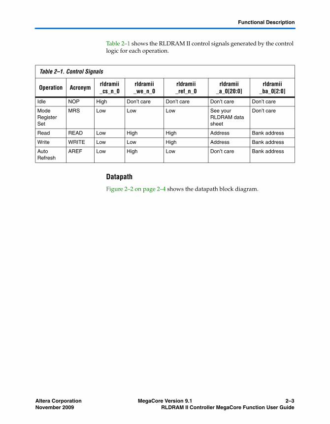
Table 2–1 shows the RLDRAM II control signals generated by the control logic for each operation.
Datapath
Figure 2–2 on page 2–4 shows the datapath block diagram.
Table 2–1. Control Signals
Operation Acronym rldramii_cs_n_0
rldramii_we_n_0
rldramii_ref_n_0
rldramii_a_0[20:0]
rldramii_ba_0[2:0]
Idle NOP High Don’t care Don’t care Don’t care Don’t care
Mode Register Set
MRS Low Low Low See your RLDRAM data sheet
Don’t care
Read READ Low High High Address Bank address
Write WRITE Low Low High Address Bank address
Auto Refresh
AREF Low High Low Don’t care Bank address
Altera Corporation MegaCore Version 9.1 2–3November 2009 RLDRAM II Controller MegaCore Function User Guide

Block Description
Figure 2–2. Datapath Block Diagram Note (1)
Note to Figure 2–2:(1) The default signal is <signal>_0. When you specify additional address and command busses, both <signal>_0 and
<signal>_1 are present.
The datapath performs the following functions:
■ Interfaces to CIO or SIO RLDRAM II devices■ Outputs write data to the RLDRAM II interface■ Captures RLDRAM II read data and data valid (QVLD) signals with:
● In DQS mode, a delayed rldramii_qk[] generated by the dedicated DQS delay circuitry
● In non-DQS mode, an external capture clock
OptionalPipeline
Registers
Datapath
rldramii_clk[]
Address &Command
OutputRegisters
OptionalPipeline
Registers
Write DataLogic
OptionalPipeline
RegistersRead DataLogic
MemoryClock
Generatorrldramii_clk_n[]
OptionalPipeline
Registers
QVLDGroup
DMGroup
DQS Group
control_dm[]control_doing_wr
control_wdata[]control_wdata_valid
control_a[]control_ba[]
control_cs_ncontrol_ref_ncontrol_we_n
control_rdata[]
capture_clk[]non_dqs_capture_clk
dqs_delay_ctrl[]
control_qvld[]
rldramii_dq[]rldramii_d[]
rldramii_q[]rldramii_qk[]
rldramii_qvld[]
rldramii_dm[]
rldramii_a_0[]rldramii_ba_0[]rldramii_cs_n_0rldramii_ref_n_0rldramii_we_n_0
2–4 MegaCore Version 9.1 Altera CorporationRLDRAM II Controller MegaCore Function User Guide November 2009
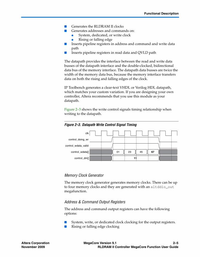
Functional Description
■ Generates the RLDRAM II clocks■ Generates addresses and commands on:
● System, dedicated, or write clock ● Rising or falling edge
■ Inserts pipeline registers in address and command and write data path
■ Inserts pipeline registers in read data and QVLD path
The datapath provides the interface between the read and write data busses of the datapath interface and the double-clocked, bidirectional data bus of the memory interface. The datapath data busses are twice the width of the memory data bus, because the memory interface transfers data on both the rising and falling edges of the clock.
IP Toolbench generates a clear-text VHDL or Verilog HDL datapath, which matches your custom variation. If you are designing your own controller, Altera recommends that you use this module as your datapath.
Figure 2–3 shows the write control signals timing relationship when writing to the datapath.
Figure 2–3. Datapath Write Control Signal Timing
Memory Clock Generator
The memory clock generator generates memory clocks. There can be up to four memory clocks and they are generated with an altddio_out megafunction.
Address & Command Output Registers
The address and command output registers can have the following options:
■ System, write, or dedicated clock clocking for the output registers.■ Rising or falling edge clocking
clk
control_doing_wr
control_wdata_valid
control_wdata[]
control_dm[]
01 23 45 6767
1111
Altera Corporation MegaCore Version 9.1 2–5November 2009 RLDRAM II Controller MegaCore Function User Guide

Block Description
Pipeline Registers
IP Toolbench can insert pipeline registers into the datapath to help meet timing at higher frequencies. IP Toolbench offers the following pipeline options:
■ Insert address and command and write data pipeline registers. The pipeline depth is the same for the write-data path and the address and command path. The write data and address and command pipeline registers are clocked off the system clock.
■ Insert read data and QVLD pipeline registers. The pipeline depth is the same for the read-data path and the QVLD path. The read data and QVLD pipeline registers are clocked off the clock that captures the read data—the delayed rldramii_qk[] signal in DQS mode; the external capture clock in non-DQS mode.
DQS Group
The datapath instantiates one or more DQS groups, which generates write data, rldramii_dq[] (CIO devices), or rldramii_d[] (SIO devices) and captures read data rldramii_dq[] (CIO devices), or rldramii_q[] (SIO devices). The IP Toolbench DQ per DQS (CIO devices) or Q per DQS (SIO devices) parameter determines the DQS group width. For example, if DQ per DQS is 9 bits, the control_wdata[] and control_rdata[] signals are 18-bits wide. To build larger widths, the datapath instantiates multiple DQS group modules to increase the data-bus width in increments of DQ per DQS (or Q per DQS) bits.
1 The datapath generates the DM output, rldramii_dm[], in the DM group module. It generates the DM output in the same way as the write data.
1 The datapath captures the QVLD input, rldramii_qvld[], in the QVLD group module. The rldramii_qvld[] signal is captured in the same way that the DQS group module captures the read data. In DQS mode, the delayed rldramii_qk[] captures rldramii_qvld[]; in non-DQS mode, the external clock captures rldramii_qvld[].
Figure 2–4 on page 2–7 shows the Stratix II series and HardCopy II devices DQS group block diagram (DQS mode, CIO devices).
2–6 MegaCore Version 9.1 Altera CorporationRLDRAM II Controller MegaCore Function User Guide November 2009

Functional Description
Figure 2–4. DQS Group Block Diagram—DQS Mode, CIO Devices Note (1), (2), (3)
Notes to Figure 2–4:(1) This figure shows the logic for one DQ output only. (2) All clocks are clk, unless marked otherwise.(3) Bus width W is dependent on the DQ per DQS parameter.(4) Invert combout of the I/O element (IOE) for the dqs pin before feeding in to inclock of the IOE for the DQ pin.
This inversion is automatic if you use an altdq megafunction for the DQ pins.
Figure 2–5 on page 2–8 shows the Stratix II series and HardCopy II devices DQS group block diagram (DQS mode, SIO devices).
DQS
DQS Delay
Q D
Q DQ D
D
Q
Q Q
D Q
D
D
Q
D Q
control_wdata
DQ
write_clk
control_doing_wr
control_rdata
dq_capture_clk
dq_oe
0
1
2W
2W
W
W
W
W
D
EN
EN
control_wdata_valid
capture_clk
Note 4
Altera Corporation MegaCore Version 9.1 2–7November 2009 RLDRAM II Controller MegaCore Function User Guide

Block Description
Figure 2–5. DQS Group Block Diagram—DQS Mode, SIO Devices Note (1), (2), (3)
Notes to Figure 2–4:(1) This figure shows the logic for one Q output and one D input only. (2) All clocks are clk, unless marked otherwise.(3) Bus width W is dependent on the Q per DQS parameter.(4) Invert combout of the I/O element (IOE) for the dqs pin before feeding in to inclock of the IOE for the Q pin.
This inversion is automatic if you use an altdq megafunction for the Q pins.
Datapath Example
Figure 2–6 shows an example datapath. The example RLDRAM II controller and memory configuration has the following parameters:
■ DQS mode■ Two 18-bit CIO RLDRAM II devices. Each RLDRAM II device has
two rldramii_qk[] data strobes, each associated with 9-bits of data
■ 36-bit RLDRAM II interface, which requires a 72-bit datapath interface
DQS
DQS Delay
Q D
Q DQ D
D
Q
Q Q
D Q
D
D
Q
D Q
control_wdata
D
Qwrite_clk
control_doing_wr
control_rdata
dq_capture_clk
dq_oe
0
1
2W
2W
W
D
EN
EN
control_wdata_valid
capture_clk
Note 4
W
W
W
2–8 MegaCore Version 9.1 Altera CorporationRLDRAM II Controller MegaCore Function User Guide November 2009

Functional Description
Figure 2–6. Example Datapath
Figure 2–6 shows the following points, which are applicable for all interface configurations:
■ Each DQS rldramii_dq[] byte group is captured by the delayed version of its associated rldramii_qk[] data strobe:
Datapath
OptionalPipeline
Registers
RLDRAM IIDevice 1
RLDRAM IIDevice 0
Read DataLogic
OptionalPipeline
Registers
QVLDGroup 1
DQS Group 3
control_rdata[35:18]
control_qvld[1]
capture_clk[1]
rldramii_dq[35:27]rldramii_qk[3]
OptionalPipeline
Registers
Read DataLogic
DQS Group 2
control_rdata[71:54]
rldramii_dq[26:18]rldramii_qk[2]
rldramii_qvld[1]
OptionalPipeline
Registers
Read DataLogic
OptionalPipeline
Registers
QVLDGroup 0
DQS Group 1
control_rdata[17:0]
control_qvld[0]
rldramii_dq[17:9]rldramii_qk[1]
OptionalPipeline
Registers
Read DataLogic
DQS Group 0
control_rdata[53:36]
rldramii_dq[8:0]rldramii_qk[0]
rldramii_qvld[0]
capture_clk[0]
Altera Corporation MegaCore Version 9.1 2–9November 2009 RLDRAM II Controller MegaCore Function User Guide

Block Description
● rldramii_dq[8:0] is captured by the delayed rldramii_qk[0]
● rldramii_dq[17:9] is captured by the delayed rldramii_qk[1]
● rldramii_dq[26:18] is captured by the delayed rldramii_qk[2]
● rldramii_dq[35:27] is captured by the delayed rldramii_qk[3]
■ QVLD is always captured by the delayed version of rldramii_qk[0] for the associated RLDRAM II device. In Figure 2–6 there are four rldramii_qk[] signals. Only rldramii_qk[0] per RLDRAM II device captures the associated QVLD signal:● rldramii_qvld[0] is captured by the delayed
rldramii_qk[0]● rldramii_qvld[1] is captured by the delayed
rldramii_qk[2]■ After the capture registers all captured read data is clocked off the
undelayed rldramii_qk[] signal that captures the QVLD signal for a particular RLDRAM II device:● All RLDRAM II 0 captured data is clocked off the undelayed
rldramii_qk[0]● All RLDRAM II 1 captured data is clocked off the undelayed
rldramii_qk[2]■ Only one capture_clk[] per attached RLDRAM II device is
output from the datapath:● RLDRAM II 0 capture data is associated with
capture_clk[0], which is the delayed rldramii_qk[0]● RLDRAM II 1 capture data is associated with
capture_clk[1], which is the delayed rldramii_qk[2]
Read Data Capture Clock Association
Figure 2–7 shows the read data and data strobes at the memory interface for the example datapath in Figure 2–6. Figure 2–8 shows how the capture_clk[] associates with the captured read data, control_rdata[] at the datapath interface.
2–10 MegaCore Version 9.1 Altera CorporationRLDRAM II Controller MegaCore Function User Guide November 2009

Functional Description
Figure 2–7. Memory Interface
Figure 2–8. Datapath Interface
Figure 2–8 shows that any read data captured on the rising edge of the delayed rldramii_qk[] signal is located in the lower half-bit locations of control_rdata[]. Any read data captured on the falling edge of the delayed rldramii_qk[] signal is located in the upper half-bit locations
rldramii_dq[35:27]
RLDRAM IIDevice 1
RLDRAM IIDevice 0
rldramii_qk[3]
rldramii_dq[26:18]
rldramii_qk[2]
rldramii_dq[17:9]
Data associated with rldramii_qk[] rising edge
rldramii_qk[1]
rldramii_dq[8:0]
rldramii_qk[0]
N PM N O P
I J K L
E F G H
A B C D
Data associated with rldramii_qk[] falling edge
capture_clk[1]
control_rdata[]
Data associated with rldramii_qk[] rising edge
capture_clk[0]
N P
J L
F H
E G
I K
M O
A C
B D
Data associated with rldramii_qk[] falling edge
Altera Corporation MegaCore Version 9.1 2–11November 2009 RLDRAM II Controller MegaCore Function User Guide

Device-Level Configuration
of control_rdata[], which means different bit ranges of the control_rdata[] are associated with different capture_clk[] signals.
1 Figure 2–8 is a specific example but the mapping and clock association applies to any RLDRAM II controller interface and memory configuration.
OpenCore Plus Time-Out Behavior
OpenCore Plus hardware evaluation can support the following two modes of operation:
■ Untethered—the design runs for a limited time■ Tethered—requires a connection between your board and the host
computer. If tethered mode is supported by all megafunctions in a design, the device can operate for a longer time or indefinitely
All megafunctions in a device time out simultaneously when the most restrictive evaluation time is reached. If there is more than one megafunction in a design, a specific megafunction’s time-out behavior may be masked by the time-out behavior of the other megafunctions.
1 For MegaCore functions, the untethered time out is 1 hour; the tethered time out value is indefinite.
Your design stops working after the hardware evaluation time expires and the controller issues no read commands at the memory interface.
f For more information on OpenCore Plus hardware evaluation, see “OpenCore Plus Evaluation” on page 1–4 and AN 320: OpenCore Plus Evaluation of Megafunctions.
Device-Level Configuration
This section describes the following topics:
■ “PLL Configuration” on page 2–12■ “Example Design” on page 2–14■ “Constraints” on page 2–16
PLL Configuration
IP Toolbench creates up to two example PLLs in your project directory, which you can parameterize to meet your exact requirements. IP Toolbench generates the example PLLs with an input to output clock ratio of 1:1 and a clock frequency you entered in IP Toolbench. In addition IP Toolbench sets the correct phase outputs on the PLLs’ clocks. You can
2–12 MegaCore Version 9.1 Altera CorporationRLDRAM II Controller MegaCore Function User Guide November 2009

Functional Description
edit the PLLs to meet your requirements with the altpll MegaWizardTM
Plug-In. IP Toolbench overwrites your PLLs in your project directory unless you turn off Update example design system PLL.
The external clocks are generated using standard I/O pins in double data rate I/O (DDIO) mode (using the altddio_out megafunction). This generation matches the way in which the write data is generated and allows better control of the skew between the clock and the data to meet the timing requirements of the RLDRAM II device.
The PLL has the following outputs:
■ Output c0 drives the system clock that clocks most of the controller including the control logic and datapath.
■ Output c1 drives the write clock that lags the system clock.■ Output c2 optionally drives the address and command clock.■ Output c3 drives the DQS DLL clock.
The recommended configuration for implementing the RLDRAM II controller in Stratix II series and HardCopy II devices is to use a single enhanced PLL to produce all the required clock signals. No external clock buffer is required as the Altera device can generate clock signals for the RLDRAM II devices.
Figure 2–9 on page 2–14 shows the recommended PLL configuration.
Altera Corporation MegaCore Version 9.1 2–13November 2009 RLDRAM II Controller MegaCore Function User Guide

Device-Level Configuration
Figure 2–9. PLL Configuration
Notes to Figure 2–9:(1) Non-DQS mode only.(2) You can connect the addr_cmd_clk RLDRAM II controller input to clk, write_clk or to the dedicated PLL
output C2.
Example Design
IP Toolbench creates an example design that shows you how to instantiate and connect up the RLDRAM II controller to an example driver. The example design is a working system that can be compiled and used for both static timing checks and board tests. It also instantiates an example PLL that generates all the required clocks for the controller. In DQS mode, a DLL is instantiated that controls the DQS capture delay phase. In non-DQS mode, the example design instantiates a fedback PLL. The output of the fedback PLL is a phase-shifted rldramii_qk[] data strobe, which captures the read data.
The example driver is a self-checking test generator for the RLDRAM II controller. It uses a state machine to write data patterns to all memory banks. It then reads back the data and checks that the data matches. If any read data fails the comparison, the pnf_per_byte output transitions low for one cycle and the pnf_persist permanent output transitions low and stays low.
Figure 2–10 shows a testbench and an example design.
Optional Fed-Back Clock
PLL (Note 1)
FPGA Device
RLDRAM II
rldramii_clk_n
rldramii_clk
rldramii_a_0[]rldramii_ba_0[]rldramii_cs_n_0rldramii_ref_n_0rldramii_we_n_0
rldramii_qk
RLDRAM II Controller
altddio
clock_source
Enhanced PLL
clk
write_clk
non_dqs_capture_clk
addr_cmd_clk(Note 2)
C0
C1
C2
C3 Stratix II DLL
altddio
Address & Command Registers
2–14 MegaCore Version 9.1 Altera CorporationRLDRAM II Controller MegaCore Function User Guide November 2009

Functional Description
Figure 2–10. Testbench & Example Design
Table 2–2 describes the files that are associated with the example design and the testbench.
The testbench instantiates an RLDRAM II model and generates a reference clock for the PLL.
1 Altera does not provide a memory simulation model. You must download one or use your own.
Example Driver
PLLclock_source
test_complete
pnf_persist
Example Design
Testbench
RLDRAM II Controller RLDRAM II Model
DLL
pnf_per_byte
Table 2–2. Example Design & Testbench Files
Filename Description
<top-level name>_tb.v or .vhd (1) Testbench for the example design.
<top-level name>.vhd or .v (1) Example design.
rldramii_pll_<device name>.vhd or .v Example PLL, which you should configure to match your frequency.
rldramii_fbpll_<device name>.vhd or .v
Fedback PLL
<variation name>_example_driver.v or .vhd (2)
Example driver.
<variation name> .v or .vhd (2) RLDRAM II controller.
Notes to Table 2–2:(1) <top-level name> is the name of the Quartus II project top-level entity.(2) <variation name> is the variation name.
Altera Corporation MegaCore Version 9.1 2–15November 2009 RLDRAM II Controller MegaCore Function User Guide

Interfaces
f For more details on how to run the simulation script, see “Simulate the Example Design” on page 3–11.
Constraints
The constraints scripts set the following constraints:
■ Sets IO standards:● 1.5 or 1.8-V HSTL voltage selection● Address and command—HSTL Class I● Data CIO mode—HSTL Class II● Data SIO mode—HSTL Class I
■ Sets output capacitance■ Places data pins as per selection in pin placement constraints floor
plan. Allows automatic placement for DQS and non-DQS modes■ Places all DM pins■ Sets up correct output enable groups■ Sets rldramii_a_0, rldramii_ba_0, rldramii_cs_n_0,
rldramii_ref_n_0 and rldrainii_we_n_0 as fast output registers (see note 1 in Table 2–5)
■ Sets rldramii_qk[] non-global signal in DQS capture mode■ Add Hold Relationship and Setup Relationship to all I/O ports.
Interfaces This section describes the following RLDRAM II commands:
■ Initialization■ Writes■ Reads■ Refreshes
Initialization
The control logic initializes the RLDRAM II devices. During initialization the mode register is set and each bank is refreshed in turn. IP Toolbench sets the following RLDRAM II initialization features:
■ On-die termination (ODT)■ Impedance matching resistor■ DLL enable■ RLDRAM II configuration
Figure 2–11 shows the initialization sequence.
2–16 MegaCore Version 9.1 Altera CorporationRLDRAM II Controller MegaCore Function User Guide November 2009

Functional Description
Figure 2–11. RLDRAM II Initialization Sequence
The mode register set (MRS) command configures the RLDRAM II devices. In the ten-cycle MRS sequence, the first nine MRS commands are dummy commands and all address bits are held at zero, to reset the RLDRAM II DLL; the final MRS command configures the memory. The RLDRAM II configuration data (CFG) is output on the rldramii_a_0[] bus during the final MRS command. The following memory parameters are setup during the final MRS command cycle:
■ RLDRAM II termination■ Impedance matching resistor■ DLL enable/disable■ RLDRAM II configuration
Writes
When you assert local_write_req, the control logic issues the write transaction immediately at the memory interface. The control logic then requests write data by asserting local_wdata_req, so that the RLDRAM II tWL period is satisfied during write transactions. This functionality means that the write request is decoupled from the write data.
Figure 2–12 shows three write requests at the local and SIO RLDRAM II interface. In this example, the memory burst length is set to eight beats. The RLDRAM II device is setup with a tRC of six-clock cycles (configuration two).
rldramii_cl k
Command
MRS = Mode Register Set CFG = Mode Register Configuration Data RFx = Refresh AC = User Command
rldramii_a[ ]
rldramii_ba[
2,048 Clock Cycles t MRSC t RC
6 x 2,048 Clock Cycles
10 Clock Cycles
200 msMinimum
]
MRS MRS RF0 RF1 RF7 AC AC
0 0 CFG Ax Ax
0 1 7 Bx Bx
Altera Corporation MegaCore Version 9.1 2–17November 2009 RLDRAM II Controller MegaCore Function User Guide

Interfaces
Figure 2–12. Write Example
Figure 2–12 shows the transactions at the local interface are separated by the correct number of clock cycles for the target RLDRAM II device configuration. If transaction requests are supplied to the RLDRAM II controller with the incorrect spacing the controller executes these transactions as requested, which can result in incorrect behavior.
Figure 2–13 shows an example of a write following a read at a CIO RLDRAM II interface. In this example, the memory burst length is set to two beats. The RLDRAM II device is setup with a tRC of six-clock cycles (configuration two).
f For more information about bus turnaround timing calculations with CIO devices, refer to AN 325: Interfacing RLDRAM II with Stratix II, Stratix & Stratix GX Devices.
clk
Local Interface
local_write_req
local_read_req
local_addr[]
local_ba[]
local_wdata_req
local_wdata[]
local_dm[]
RLDRAM II Interface
rldramii_clk
rldramii_clk_n
rldramii_cs_n
rldramii_we_n
rldramii_ref_n
rldramii_a[]
rldramii_ba[]
A B CC
A B CC
A01 A23A45 A67 B01 B23 B45B67 C01 C23 C45 C67
00
A B CB
A B CB
rldramii_d[]
rldramii_qk[]
rldramii_qvld[]
rldramii_q[]
0 1 2 3 4 5 6 7 0 1 2 3 4 5 6 7 0 1 2 3 4 5 6 77
rldramii_dm[] 11 1100
2–18 MegaCore Version 9.1 Altera CorporationRLDRAM II Controller MegaCore Function User Guide November 2009

Functional Description
Figure 2–13. Write Following a Read
Reads
When you assert local_read_req, the control logic issues the read transaction immediately at the memory interface.
In DQS mode the read data, rldramii_dq[] (CIO devices) or rldramii_q[] (SIO devices), and the QVLD signals, rldramii_qvld[], are captured using the delayed rldramii_qk[] data strobes that have been phase shifted using the dedicated DQS delay circuitry.
In non-DQS mode the read data, rldramii_dq[] or rldramii_q[], and the QVLD signals, rldramii_qvld[], are captured using an external capture clock.
clk
Local_Interface
local_write_req
local_read_req
local_addr[]
local_ba[]
local_wdata_req
local_wdata[]
local_dm[]
RLDRAM_II_Interface
rldramii_clk
rldramii_clk_n
rldramii_cs_n
rldramii_we_n
rldramii_ref_n
rldramii_a[]
rldramii_ba[]
rldramii_dm[]
rldramii_dq[ ]
rldramii_qk[]
rldramii_qvld[]
A BB
A BB
00
01
A BA
A BA
11 110000
0 1 0 11
Altera Corporation MegaCore Version 9.1 2–19November 2009 RLDRAM II Controller MegaCore Function User Guide

Interfaces
During reads, the local interface indicates that read data is valid by asserting the local_rdata_valid[] signal. All captured read data is clocked off the clock that captures the RLDRAM II read data. In DQS mode, this clock is the delayed DQS signal, capture_clk[], sourced from the dedicated DQS delay circuitry. In non-DQS mode this clock is the external capture clock, non_dqs_capture_clk.
Figure 2–14 shows an example of a read at an SIO RLDRAM II interface. In this example, the memory burst length is set to eight beats. The RLDRAM II device is setup with a tRC of six-clock cycles (configuration two).
Figure 2–14. Read Example
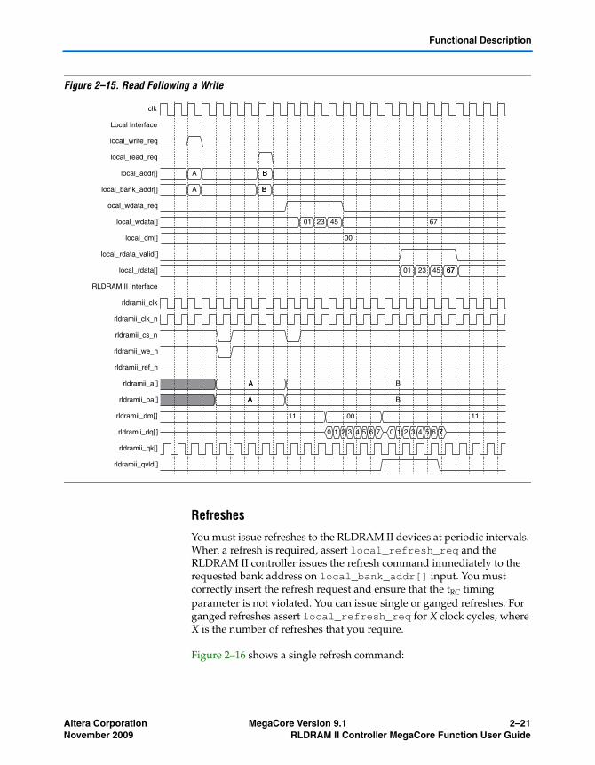
Figure 2–15 shows an example of a read following a write at a CIO RLDRAM II interface. In this example, the memory burst length is set to eight beats. The RLDRAM II device is setup with a tRC of six-clock cycles (configuration two).
f For more information about bus turnaround timing calculations with CIO devices, refer to AN 325: Interfacing RLDRAM II with Stratix II, Stratix & Stratix GX Devices.
clk
Local Interface
local_read_req
local_write_req
local_addr[]
local_bank_addr[]
local_rdata_valid[]
local_rdata[]
RLDRAM II Interface
rldramii_clk
rldramii_clk_n
rldramii_cs_n
rldramii_we_n
rldramii_ref_n
rldramii_a[]
rldramii_ba[]
rldramii_dm[ ]
rldramii_d[]
rldramii_qk[]
rldramii_qvld[]
rldramii_q[]
A B CC
A B CC
A01 A23A45 A67 B01 B23B45 B67C01 C23C45 C67C67
A B CB
A B CB
11
0 1 2 3 4 5 6 7 0 1 2 3 4 5 6 7 0 1 2 3 4 5 6 77
2–20 MegaCore Version 9.1 Altera CorporationRLDRAM II Controller MegaCore Function User Guide November 2009
Functional Description
Figure 2–15. Read Following a Write
Refreshes
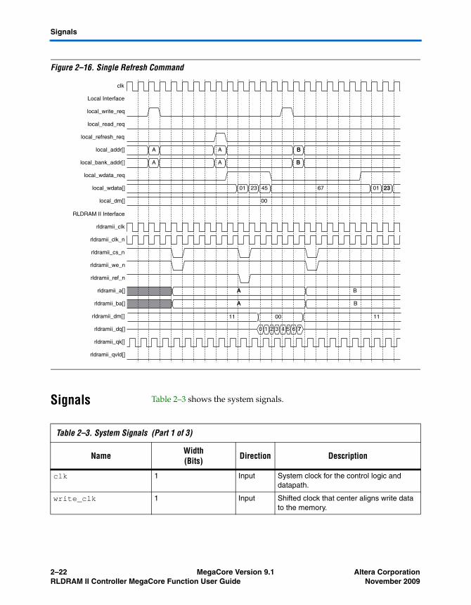
You must issue refreshes to the RLDRAM II devices at periodic intervals. When a refresh is required, assert local_refresh_req and the RLDRAM II controller issues the refresh command immediately to the requested bank address on local_bank_addr[] input. You must correctly insert the refresh request and ensure that the tRC timing parameter is not violated. You can issue single or ganged refreshes. For ganged refreshes assert local_refresh_req for X clock cycles, where X is the number of refreshes that you require.
Figure 2–16 shows a single refresh command:
clk
Local Interface
local_write_req
local_read_req
local_addr[]
local_bank_addr[]
local_wdata_req
local_wdata[]
local_dm[]
local_rdata_valid[]
local_rdata[]
RLDRAM II Interface
rldramii_clk
rldramii_clk_n
rldramii_cs_n
rldramii_we_n
rldramii_ref_n
rldramii_a[]
rldramii_ba[]
rldramii_dm[]
rldramii_dq[ ]
rldramii_qk[]
rldramii_qvld[]
A BB
A BB
01 23 45 67
00
01 23 45 6767
A BA
A BA
0 1 2 3 4 5 6 7 0 1 2 3 4 5 6 77
11 1100
Altera Corporation MegaCore Version 9.1 2–21November 2009 RLDRAM II Controller MegaCore Function User Guide
Signals
Figure 2–16. Single Refresh Command
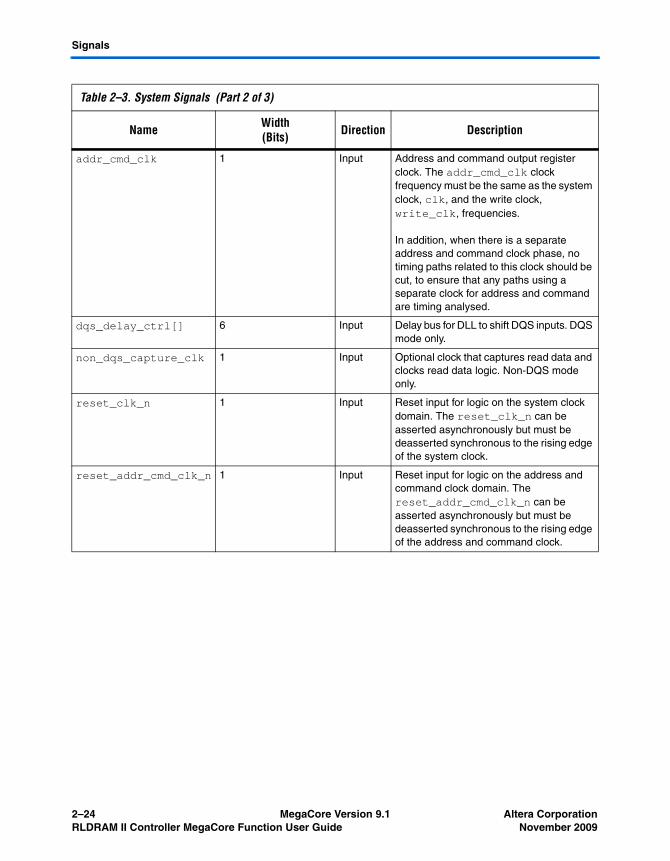
Signals Table 2–3 shows the system signals.
clk
Local Interface
local_write_req
local_read_req
local_refresh_req
local_addr[]
local_bank_addr[]
local_wdata_req
local_wdata[]
local_dm[]
RLDRAM II Interface
rldramii_clk
rldramii_clk_n
rldramii_cs_n
rldramii_we_n
rldramii_ref_n
rldramii_a[]
rldramii_ba[]
rldramii_dm[]
rldramii_dq[]
rldramii_qk[]
rldramii_qvld[]
A A BB
A A BB
01 23 45 67 01 2323
00
A BA
A BA
0 1 2 3 4 5 6 77
11 1100
Table 2–3. System Signals (Part 1 of 3)
Name Width(Bits) Direction Description
clk 1 Input System clock for the control logic and datapath.
write_clk 1 Input Shifted clock that center aligns write data to the memory.
2–22 MegaCore Version 9.1 Altera CorporationRLDRAM II Controller MegaCore Function User Guide November 2009

Functional Description
addr_cmd_clk 1 Input Address and command output register clock. The addr_cmd_clk clock frequency must be the same as the system clock, clk, and the write clock, write_clk, frequencies.
In addition, when there is a separate address and command clock phase, no timing paths related to this clock should be cut, to ensure that any paths using a separate clock for address and command are timing analysed.
dqs_delay_ctrl[] 6 Input Delay bus for DLL to shift DQS inputs. DQS mode only.
non_dqs_capture_clk 1 Input Optional clock that captures read data and clocks read data logic. Non-DQS mode only.
reset_clk_n 1 Input Reset input for logic on the system clock domain. The reset_clk_n can be asserted asynchronously but must be deasserted synchronous to the rising edge of the system clock.
reset_addr_cmd_clk_n 1 Input Reset input for logic on the address and command clock domain. The reset_addr_cmd_clk_n can be asserted asynchronously but must be deasserted synchronous to the rising edge of the address and command clock.
Table 2–3. System Signals (Part 2 of 3)
Name Width(Bits) Direction Description
Altera Corporation MegaCore Version 9.1 2–23November 2009 RLDRAM II Controller MegaCore Function User Guide
Signals
addr_cmd_clk 1 Input Address and command output register clock. The addr_cmd_clk clock frequency must be the same as the system clock, clk, and the write clock, write_clk, frequencies.
In addition, when there is a separate address and command clock phase, no timing paths related to this clock should be cut, to ensure that any paths using a separate clock for address and command are timing analysed.
dqs_delay_ctrl[] 6 Input Delay bus for DLL to shift DQS inputs. DQS mode only.
non_dqs_capture_clk 1 Input Optional clock that captures read data and clocks read data logic. Non-DQS mode only.
reset_clk_n 1 Input Reset input for logic on the system clock domain. The reset_clk_n can be asserted asynchronously but must be deasserted synchronous to the rising edge of the system clock.
reset_addr_cmd_clk_n 1 Input Reset input for logic on the address and command clock domain. The reset_addr_cmd_clk_n can be asserted asynchronously but must be deasserted synchronous to the rising edge of the address and command clock.
Table 2–3. System Signals (Part 2 of 3)
Name Width(Bits) Direction Description
2–24 MegaCore Version 9.1 Altera CorporationRLDRAM II Controller MegaCore Function User Guide November 2009

Functional Description
Table 2–4 shows the local interface signals.
reset_read_clk_n[] DQS mode: the number of RLDRAM II devices attached to the memory interface
Non-DQS mode:1
Input Reset input for logic on the capture clock domain. In DQS mode, the capture clock domain is capture_clk[]; in non-DQS mode, it is non_dqs_capture_clk. In DQS mode, each reset_read_clk_n[] is associated with the corresponding capture_clk[] clock domain. The reset_read_clk_n[] can be asserted asynchronously but must be deasserted synchronous to the rising edge of the capture clock.
capture_clk[] The number of RLDRAM II devices attached to memory interface
Output Undelayed DQS clock used by capture circuitry to capture RLDRAM II read data. There is one capture_clk[] per attached RLDRAM II device. DQS mode only.
Table 2–3. System Signals (Part 3 of 3)
Name Width(Bits) Direction Description
Table 2–4. Local Interface Signals (Part 1 of 2)
Name Width(Bits) Direction Description
local_addr[] Device dependant Input RLDRAM II address. IP Toolbench refers to the memory.dat file and selects the address width appropriate to the device.
local_bank_addr[] 3 – RLDRAM II bank address.
local_dm[] The number of RLDRAM II devices attached to the memory interface × 2
Input Optional local data mask (DM). Twice the width of the memory rldramii_dm[] bus. When all high, all writes are masked.
local_read_req 1 Input Read request signal.
local_refresh_req 1 Input User controlled refresh request. This allows complete control over when refreshes are issued to the memory. The refresh is issued to the bank address on local_bank_addr[].
Altera Corporation MegaCore Version 9.1 2–25November 2009 RLDRAM II Controller MegaCore Function User Guide

Signals
Table 2–5 shows the memory interface signals.
local_wdata[] Data-bus width × 2 Input Write data bus. The local interface must request local_wdata[] over multiple clock cycles to construct the write data for any requested write bursts. If the memory burst length is set to two beats, the write data is requested in a single clock cycle at the local interface.
local_write_req 1 Input Write request signal.
local_init_done 1 Output Memory initialization complete signal which is asserted when the controller has completed its initialization of the memory. Reads and writes should not be requested until local_init_done is asserted.
local_rdata[] Data-bus width × 2 Output Read data bus. The controller returns local_rdata[] over multiple clock cycles for any requested read transactions. If the memory burst length is set to two beats, the read data is returned in a single clock cycle at the local interface.
local_rdata_valid[]
The number of RLDRAM II devices attached to memory interface
Output Read data valid signal, which indicates that valid data is present on the read data bus. The local_rdata_valid[] signal is aligned with the local read data, local_rdata[]. There is only one local_rdata_valid[] per attached RLDRAM II device.
local_wdata_req 1 Output Write data request signal. When the local interface asserts local_wdata_req, all the write data for the burst should be available in contiguous clock cycles.
Table 2–4. Local Interface Signals (Part 2 of 2)
Name Width(Bits) Direction Description
Table 2–5. Memory Interface Signals (Part 1 of 2)
Name Width(Bits) Direction Description
rldramii_dq[] Data-bus width Bidirectional Memory data bus. CIO devices only.
rldramii_qk[] 1 to 9 Bidirectional In DQS mode, the memory data strobe signal that captures read data into the Altera device; in non-DQS mode, the RLDRAM II controller does not use rldramii_qk[].
rldramii_q[] Data-bus width Input Memory read data bus. SIO devices only.
2–26 MegaCore Version 9.1 Altera CorporationRLDRAM II Controller MegaCore Function User Guide November 2009

Functional Description
rldramii_qvld[] The number of RLDRAM II devices attached to memory interface
Input Read data valid flag.
rldramii_a_0[]rldramii_a_1[] (1)
local_addr[] Output Memory address signals.
rldramii_ba_0[]rldramii_ba_1[] (1)
3 Output Memory bank address signals.
rldramii_clk[], rldramii_clk_n[]
1 to 3 (wtih dedicated PLL clocks) or 1 to 8 otherwise
Output Memory command output clock.
rldramii_cs_n_0rldramii_cs_n_1 (1)
1 Output Memory chip select signal.
rldramii_d[] Data-bus width Output Memory write data bus. SIO devices only.
rldramii_dm[] The number of RLDRAM II devices attached to memory interface
Output Memory DM (optional).
rldramii_ref_n_0rldramii_ref_n_1 (1)
1 Output Memory refresh request signal.
rldramii_we_n_0rldramii_we_n_1 (1)
1 Output Memory write enable signal.
Note to Table 2–5:(1) The default signal is <signal>_0. When you specify additional address and command busses, both <signal>_0 and
<signal>_1 are present.
Table 2–5. Memory Interface Signals (Part 2 of 2)
Name Width(Bits) Direction Description
Altera Corporation MegaCore Version 9.1 2–27November 2009 RLDRAM II Controller MegaCore Function User Guide

Parameters
Table 2–6 shows the datapath interface signals.
Parameters The parameters can only be set in IP Toolbench (see “Step 1: Parameterize” on page 3–5).
Table 2–6. Datapath Interface Signals
Name Width(Bits) Direction Description
control_a[] local_addr[] Input Address bits.
control_ba[] 3 Input Bank address bits.
control_cs_n 1 Input Chip select signal.
control_dm[] The number of RLDRAM II devices attached to the memory interface × 2
Input The DM bus, which has valid data in the same clock cycles that control_wdata_valid is asserted.
control_doing_wr 1 Input Control_doing_wr is asserted when the controller is writing to the RLDRAM II devices and controls the output enables on rldramii_dq[] or rldramii_d[].
control_ref_n 1 Input Refresh signal.
control_wdata[] Data-bus width × 2 Input The write data bus, which has valid data in the same clock cycles that control_wdata_valid is asserted.
control_wdata_valid
1 Input Enables the write data bus and DM enable registers so that they are only updated when valid data and enables are available.
control_we_n 1 Input Write enable signal.
control_qvld[] The number of RLDRAM II devices attached to the memory interface
Output The read data valid flag.There is only one QVLD flag per RLDRAM II device. The control_qvld[] signal is aligned with the valid control_rdata[] and is asserted during this period. The control_qvld[] signal has the same functionality as local_rdata_valid[].
control_rdata[] Data-bus width × 2 Output The captured read data (same as local_rdata[]).
2–28 MegaCore Version 9.1 Altera CorporationRLDRAM II Controller MegaCore Function User Guide November 2009
Functional Description
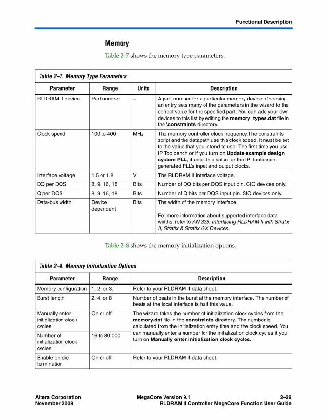
Memory
Table 2–7 shows the memory type parameters.
Table 2–8 shows the memory initialization options.
Table 2–7. Memory Type Parameters
Parameter Range Units Description
RLDRAM II device Part number – A part number for a particular memory device. Choosing an entry sets many of the parameters in the wizard to the correct value for the specified part. You can add your own devices to this list by editing the memory_types.dat file in the \constraints directory.
Clock speed 100 to 400 MHz The memory controller clock frequency.The constraints script and the datapath use this clock speed. It must be set to the value that you intend to use. The first time you use IP Toolbench or if you turn on Update example design system PLL, it uses this value for the IP Toolbench-generated PLL’s input and output clocks.
Interface voltage 1.5 or 1.8 V The RLDRAM II interface voltage.
DQ per DQS 8, 9, 16, 18 Bits Number of DQ bits per DQS input pin. CIO devices only.
Q per DQS 8, 9, 16, 18 Bits Number of Q bits per DQS input pin. SIO devices only.
Data-bus width Device dependent
Bits The width of the memory interface.
For more information about supported interface data widths, refer to AN 325: Interfacing RLDRAM II with Stratix II, Stratix & Stratix GX Devices.
Table 2–8. Memory Initialization Options
Parameter Range Description
Memory configuration 1, 2, or 3. Refer to your RLDRAM II data sheet.
Burst length 2, 4, or 8 Number of beats in the burst at the memory interface. The number of beats at the local interface is half this value.
Manually enter initialization clock cycles
On or off The wizard takes the number of initialization clock cycles from the memory.dat file in the constraints directory. The number is calculated from the initialization entry time and the clock speed. You can manually enter a number for the initialization clock cycles if you turn on Manually enter initialization clock cycles.
Number of initialization clock cycles
16 to 80,000
Enable on-die termination
On or off Refer to your RLDRAM II data sheet.
Altera Corporation MegaCore Version 9.1 2–29November 2009 RLDRAM II Controller MegaCore Function User Guide
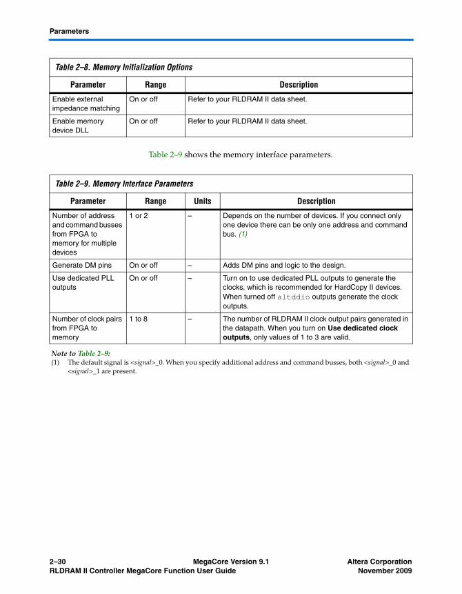
Parameters
Table 2–9 shows the memory interface parameters.
Enable external impedance matching
On or off Refer to your RLDRAM II data sheet.
Enable memory device DLL
On or off Refer to your RLDRAM II data sheet.
Table 2–8. Memory Initialization Options
Parameter Range Description
Table 2–9. Memory Interface Parameters
Parameter Range Units Description
Number of address and command busses from FPGA to memory for multiple devices
1 or 2 – Depends on the number of devices. If you connect only one device there can be only one address and command bus. (1)
Generate DM pins On or off – Adds DM pins and logic to the design.
Use dedicated PLL outputs
On or off – Turn on to use dedicated PLL outputs to generate the clocks, which is recommended for HardCopy II devices. When turned off altddio outputs generate the clock outputs.
Number of clock pairs from FPGA to memory
1 to 8 – The number of RLDRAM II clock output pairs generated in the datapath. When you turn on Use dedicated clock outputs, only values of 1 to 3 are valid.
Note to Table 2–9:(1) The default signal is <signal>_0. When you specify additional address and command busses, both <signal>_0 and
<signal>_1 are present.
2–30 MegaCore Version 9.1 Altera CorporationRLDRAM II Controller MegaCore Function User Guide November 2009

Functional Description
Timing
Table 2–10 shows the pipeline options.
Table 2–11 shows the clocking modes.
Table 2–10. Pipeline Options
Parameter Range Description
Number of address and command and write data pipeline registers
0, 1, 2 or 3 When you choose 1, 2, or 3 the wizard inserts 1, 2, or 3 pipeline registers between the memory controller and the command and address output registers and the write data output registers. These registers may help to achieve the required performance at higher frequencies.
Number of read data pipeline registers
0, 1, 2 or 3 When you choose 1, 2, or 3 the wizard inserts 1, 2, or 3 pipeline registers between the read capture registers and the memory controller. These registers may help to achieve the required performance at higher frequencies.
Table 2–11. Clocking Modes
Parameter Range Description
Address and command clock
System, write, or dedicated
The clock for the address and command output registers. For system_clk choose System; for write_clk, choose Write, and for a separate clock, choose Dedicated.
If you choose Dedicated for the clock, ensure the clock phase allows the Quartus II software to meet the setup time on the address and command output registers.
Address and command clock edge
Falling or rising The clock edge on which the addresses and commands are output.
Dedicated address and command clock PLL phase offset
± 180 Sets the dedicated address and command clock PLL phase for better timing.
Enable DQS mode On or off Turn on for DQS mode; otherwise the controller is in non-DQS mode (Stratix II and Stratix II GX devices only). HardCopy II devices allow DQS mode only.
Use migratable byte groups
On or off When turned on, you can migrate the design to a migration device. When turned off the wizard allows much greater flexibility in the placement of byte groups. You can only turn on this option when Enable DQS mode is turned off.
Fedback PLL phase offset
± 180 Sets the fedback clock PLL phase for read capture (non-DQS mode only).
Altera Corporation MegaCore Version 9.1 2–31November 2009 RLDRAM II Controller MegaCore Function User Guide

Parameters
Table 2–12 shows the pin loading parameters.
Project Settings
Table 2–13 shows the example design settings.
Table 2–12. Pin Loading Parameters
Parameter Range (pF) Description
Pin loading on FPGA DQ/DQS pins
0 to 100 Enter the pin loading to match your board and memory devices.
Pin loading on FPGA address and command pins
0 to 100 Enter the pin loading to match your board and memory devices.
Pin loading on FPGA clock pins
0 to 100 Enter the pin loading to match your board and memory devices.
Table 2–13. Example Design Settings
Parameter Description
Automatically apply RLDRAM II controller-specific constraints to the Quartus II project
When this option is turned on, the next time you compile, the Quartus II software automatically runs the add constraints script. Turn off this option if you do not want the script to run automatically.
Update the example design file that instantiates the RLDRAM II controller variation
When this option is turned on, IP Toolbench parses and updates the example design file. It only updates sections that are between the following markers:<<START MEGAWIZARD INSERT <tagname><<END MEGAWIZARD INSERT <tagname>
If you edit the example design file, ensure that your changes are outside of the markers or remove the markers. Once you remove the markers, you must keep the file updated, because IP Toolbench can no longer update the file.
Update example design system PLL
When this option is turned on, IP Toolbench automatically overwrites the PLL.Turn off this option, if you do not want the wizard to overwrite the PLL.
2–32 MegaCore Version 9.1 Altera CorporationRLDRAM II Controller MegaCore Function User Guide November 2009

Functional Description
Table 2–14 shows the variation path parameters.
Table 2–15 shows the device pin prefixes parameter.
MegaCore Verification
MegaCore verification involves simulation testing and hardware testing.
Simulation Environment
Altera has carried out extensive functional tests using industry-standard models to ensure the functionality of the RLDRAM II controller. In addition, Altera has carried out a wide variety of gate-level tests on the RLDRAM II controller to verify the post-compilation functionality of the controller.
Hardware Testing
Table 2–16 shows the Altera development board on which Altera hardware tested the RLDRAM II controller.
Table 2–14. Variation Path Parameters
Parameter Description
Enable hierarchy control The constraints script analyzes your design, to automatically extract the hierarchy to your variation. To prevent the constraints script analyzing your design, turn on Enable Hierarchy Control, and enter the correct hierarchy path to your datapath.
Hierarchy path to RLDRAM II controller datapath
The hierarchy path is the path to your RLDRAM II controller datapath, minus the top-level name. The hierarchy entered in the wizard must match your design, because the constraints scripts rely on this path for correct operation.
Table 2–15. Device Pin Prefixes
Parameter Description
Prefix all RLDRAM II pins on the device with
This string prefixes the pin names for the FPGA pins that are connected to the RLDRAM II controller.
Table 2–16. Altera Development Boards
Development Board Altera Device Memory Device
Stratix II Memory Demonstration Board 1 EP2S60F1020C3 Micron 18-bit CIO and SIO RLDRAM II devices
Altera Corporation MegaCore Version 9.1 2–33November 2009 RLDRAM II Controller MegaCore Function User Guide

MegaCore Verification
2–34 MegaCore Version 9.1 Altera CorporationRLDRAM II Controller MegaCore Function User Guide November 2009

Altera Corporation MNovember 2009
3. Getting Started
Design Flow To evaluate the RLDRAM II Controller MegaCore function using the OpenCore Plus feature, include these steps in your design flow:
1. Obtain and install the RLDRAM II Controller MegaCore Function.
The RLDRAM II Controller is part of the MegaCore IP Library, which is distributed with the Quartus II software and downloadable from the Altera website, www.altera.com.
f For system requirements and installation instructions, refer to Altera Software Installation and Licensing.
Figure 3–1 shows the directory structure after you install the RLDRAM II Controller, where <path> is the installation directory. The default installation directory on Windows is c:\altera\<version>; on Linux it is /opt/altera<version>.
Figure 3–1. RLDRAM II Controller Directory Structure
2. Create a custom variation of the RLDRAM II Controller MegaCore function using IP Toolbench.
commonContains shared components.
rldram_ii_controllerContains the RLDRAM II Controller MegaCore function files and documentation.
docContains the documentation for the RLDRAM II Controller MegaCore function.
constraintsContains scripts that generate an instance-specific Tcl script for each instance of the RLDRAM II Controller in various Altera devices.
datContains a data file for each Altera device combination that is used by the Tcl script to generate the instance-specific Tcl script.
libContains encrypted lower-level design files and other support files.
alteraContains the Altera MegaCore IP Library.
ipContains the Altera MegaCore IP Library and third-party IP cores.
<path>Installation directory.
egaCore Version 9.1 3–1
RLDRAM II Controller Walkthrough
1 IP Toolbench is a toolbar from which you quickly and easily view documentation, specify parameters, and generate all of the files necessary for integrating the parameterized MegaCore function into your design.
3. Implement the rest of your design using the design entry method of your choice.
4. Use the IP Toolbench-generated IP functional simulation model to verify the operation of your design.
f For more information on IP functional simulation models, refer to the Simulating Altera IP in Third-Party Simulation Tools chapter in volume 3 of the Quartus II Handbook.
5. Edit the PLL.
6. Use the Quartus II software to add constraints to the example design and compile the example design.
7. Perform gate-level timing simulation, or if you have a suitable development board, you can generate an OpenCore Plus time-limited programming file, which you can use to verify the operation of the example design in hardware.
8. Either obtain a license for the RLDRAM II controller MegaCore function or replace the encrypted RLDRAM II controller control logic with your own logic and use the clear-text datapath.
1 If you obtain a license for the RLDRAM II controller, you must set up licensing.
9. Generate a programming file for the Altera device(s) on your board.
10. Program the Altera device(s) with the completed design.
RLDRAM II Controller Walkthrough
This walkthrough explains how to create a RLDRAM II controller using the Altera RLDRAM II controller IP Toolbench and the Quartus II software on a PC. When you are finished generating a custom variation of the RLDRAM II controller MegaCore function, you can incorporate it into your overall project.
This walkthrough requires the following steps:
■ “Create a New Quartus II Project” on page 3–3■ “Launch IP Toolbench” on page 3–4
3–2 MegaCore Version 9.1 Altera CorporationRLDRAM II Controller MegaCore Function User Guide November 2009

Getting Started
■ “Step 1: Parameterize” on page 3–5■ “Step 2: Constraints” on page 3–7■ “Step 3: Set Up Simulation” on page 3–8■ “Step 4: Generate” on page 3–8
Create a New Quartus II Project
You need to create a new Quartus II project with the New Project Wizard, which specifies the working directory for the project, assigns the project name, and designates the name of the top-level design entity. To create a new project follow these steps:
1. Choose Programs > Altera > Quartus II <version> (Windows Start menu) to run the Quartus II software. Alternatively, you can use the Quartus II Web Edition software.
2. Choose New Project Wizard (File menu).
3. Click Next in the New Project Wizard Introduction page (the introduction page does not display if you turned it off previously).
4. In the New Project Wizard: Directory, Name, Top-Level Entity page, enter the following information:
a. Specify the working directory for your project. For example, this walkthrough uses the c:\altera\projects\rldram_project directory.
b. Specify the name of the project. This walkthrough uses project for the project name.
1 The Quartus II software automatically specifies a top-level design entity that has the same name as the project. Do not change it.
5. Click Next to close this page and display the New Project Wizard: Add Files page.
1 When you specify a directory that does not already exist, a message asks if the specified directory should be created. Click Yes to create the directory.
6. If you installed the MegaCore IP Library in a different directory from where you installed the Quartus II software, you must add the user libraries:
a. Click User Libraries.
Altera Corporation MegaCore Version 9.1 3–3November 2009 RLDRAM II Controller MegaCore Function User Guide

RLDRAM II Controller Walkthrough
b. Type <path>\ip into the Library name box, where <path> is the directory in which you installed the RLDRAM II controller.
c. Click Add to add the path to the Quartus II project.
d. Click OK to save the library path in the project.
7. Click Next to close this page and display the New Project Wizard: Family & Device Settings page.
8. On the New Project Wizard: Family & Device Settings page, choose the target device family in the Family list.
9. The remaining pages in the New Project Wizard are optional. Click Finish to complete the Quartus II project.
You have finished creating your new Quartus II project.
Launch IP Toolbench
To launch IP Toolbench in the Quartus II software, follow these steps:
1. Start the MegaWizard® Plug-In Manager by choosing MegaWizard Plug-In Manager (Tools menu). The MegaWizard Plug-In Manager dialog box displays.
1 Refer to Quartus II Help for more information on how to use the MegaWizard Plug-In Manager.
2. Specify that you want to create a new custom megafunction variation and click Next.
3. Expand the Interfaces > Memory Controllers directory, then click RLDRAM II Controller v9.1.
4. Select the output file type for your design; the wizard supports VHDL and Verilog HDL.
5. The MegaWizard Plug-In Manager shows the project path that you specified in the New Project Wizard. Append a variation name for the MegaCore function output files <project path>\<variation name>.
1 The <variation name> must be a different name from the project name and the top-level design entity name.
6. Click Next to launch IP Toolbench.
3–4 MegaCore Version 9.1 Altera CorporationRLDRAM II Controller MegaCore Function User Guide November 2009

Getting Started
Step 1: Parameterize
To parameterize your MegaCore function, follow these steps:
f For more information on parameters, refer to “Parameters” on page 2–28.
1. Click Step 1: Parameterize in IP Toolbench .
2. Choose the memory type.
a. Choose the memory device.
1 You can add your own memory devices to this list by editing the memory_types.dat file in the \constraints directory.
b. Enter the clock speed.
c. Choose the interface voltage.
d. Choose the data bus width.
e. Choose the DQ per DQS (CIO devices), or the Q per DQS (SIO devices).
3. Choose the memory initialization options.
4. Choose your memory interface parameters.
5. Click the Timing tab.
f For more information on timing parameters, refer to “Timing” on page 2–31.
6. Enter the datapath pipeline options.
7. Choose the clocking modes.
8. Turn on the appropriate capture mode—DQS or non-DQS capture mode. If you turn off Enable DQS mode (non-DQS capture mode), you can turn on Use migratable bytegroups.
9. Click the Project Settings tab.
f For more information on project settings, refer to “Project Settings” on page 2–32.
Altera Corporation MegaCore Version 9.1 3–5November 2009 RLDRAM II Controller MegaCore Function User Guide
RLDRAM II Controller Walkthrough
10. Altera recommends that you turn on Automatically apply RLDRAM II controller-specific constraints to the Quartus II project so that the Quartus II software automatically applies the constraints script when you compile the example design.
1 You must turn on this option, the first time you run IP Toolbench.
11. Ensure Update the example design file that instantiates the RLDRAM II controller variation is turned on, for IP Toolbench to automatically update the example design file.
1 You must turn on this option, the first time you run IP Toolbench.
12. Turn off Update example design system PLL, if you have edited the PLL and you do not want the wizard to regenerate the PLL when you regenerate the variation.
1 You must turn on this option, the first time you run IP Toolbench.
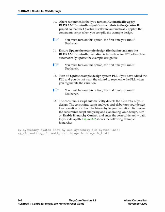
13. The constraints script automatically detects the hierarchy of your design. The constraints script analyzes and elaborates your design to automatically extract the hierarchy to your variation. To prevent the constraints script analyzing and elaborating your design, turn on Enable Hierarchy Control, and enter the correct hierarchy path to your datapath. Figure 3–2 shows the following example hierarchy:
my_system:my_system_inst|my_sub_system:my_sub_system_inst|my_rldramii:my_rldramii_inst|datapath:datapath_inst|
3–6 MegaCore Version 9.1 Altera CorporationRLDRAM II Controller MegaCore Function User Guide November 2009

Getting Started
Figure 3–2. System Naming
14. IP Toolbench uses a prefix (for example, rldramii_) for the names of all memory interface pins. Enter a prefix for all memory interface pins associated with this custom variation.
15. Enter the pin loading for the FPGA pins.
1 You must enter suitable values for the pin loading, because the values affect timing.
16. Click Finish.
Step 2: Constraints
To choose the constraints for your device, follow these steps:
1. Click Step 2: Constraints in IP Toolbench.
2. Choose the positions on the device for each of the RLDRAM II byte groups. To place a byte group, select the byte group in the drop-down box at your chosen position.
1 The floorplan matches the orientation of the Quartus II floorplanner. The layout represents the die as viewed from above. A byte group consists of data (DQ) pins for CIO devices; or data (Q) pins for SIO devices, and a data strobe signal (DQS) pin. The number of data pins per byte group matches your choice of DQ (or Q) per DQS.
RLDRAM II
Datapath
Other Logic
PLL
RLDRAM II Interface
example_topExample Top-Level Design
my_rldramRLDRAM II Controller
my_systemSystem
my_sub_systemSubystem
Altera Corporation MegaCore Version 9.1 3–7November 2009 RLDRAM II Controller MegaCore Function User Guide

RLDRAM II Controller Walkthrough
Step 3: Set Up Simulation
An IP functional simulation model is a cycle-accurate VHDL or Verilog HDL model produced by the Quartus II software. The model allows for fast functional simulation of IP using industry-standard VHDL and Verilog HDL simulators.
c You may only use these simulation model output files for simulation purposes and expressly not for synthesis or any other purposes. Using these models for synthesis will create a nonfunctional design.
To generate an IP functional simulation model for your MegaCore function, follow these steps:
1. Click Step 3: Set Up Simulation in IP Toolbench.
2. Turn on Generate Simulation Model.
3. Choose the language in the Language list.
4. Some third-party synthesis tools can use a netlist that contains only the structure of the MegaCore function, but not detailed logic, to optimize performance of the design that contains the MegaCore function. If your synthesis tool supports this feature, turn on Generate netlist.
5. Click OK.
Step 4: Generate
To generate your MegaCore function, click Step 4: Generate in IP Toolbench.
3–8 MegaCore Version 9.1 Altera CorporationRLDRAM II Controller MegaCore Function User Guide November 2009

Getting Started
Table 3–1 describes the generated files and other files that may be in your project directory. The names and types of files specified in the IP Toolbench report vary based on whether you created your design with VHDL or Verilog HDL
Table 3–1. Generated Files (Part 1 of 2) Note (1), (2), (3)
Filename Description
<variation name>.vhd, or .v A MegaCore function variation file, which defines a VHDL or Verilog HDL description of the custom MegaCore function. Instantiate the entity defined by this file inside of your design. Include this file when compiling your design in the Quartus II software.
<variation name>.cmp A VHDL component declaration file for the MegaCore function variation. Add the contents of this file to any VHDL architecture that instantiates the MegaCore function.
<variation name>.bsf Quartus II symbol file for the MegaCore function variation. You can use this file in the Quartus II block diagram editor.
<variation name>.sdc A Synopsys Design Constraints (SDC) file. Use this SDC file with the DDR timing wizard (DTW)-generated SDC file when using TimeQuest. You must copy the contents of this file into the DTW-generated SDC file, so the example design has the correct timing constraints when using TimeQuest.
altera_vhdl_support.vhd A VHDL package that contains functions for the generated entities. This file may be shared between MegaCore functions.
<variation name>_example_driver.vhd or .v Example driver.
<top-level name>.vhd or .v Example design file.
add_constraints_for_<variation name>.tcl Add constraints script.
rldramii_pll_<device name>.vhd or .v System PLL.
rldramii_fbpll_<device name>.vhd or .v Fedback PLL.
<variation name>_auk_rldramii_addr_cmd_reg.vhd or .v
Address and command output registers.
<variation name>_auk_rldramii_clk_gen.vhd or .v Memory clock generator.
<variation name>_auk_rldramii_controller_ipfs_wrapper.vhd or .v
A file that instantiates the controller.
<variation name>_auk_rldramii_controller_ipfs_wrapper.vho or .vo
VHDL or Verilog HDL IP functional simulation model.
<variation name>_auk_rldramii_datapath.vhd or .v Datapath.
Altera Corporation MegaCore Version 9.1 3–9November 2009 RLDRAM II Controller MegaCore Function User Guide

RLDRAM II Controller Walkthrough
1. After you review the generation report, click Exit to close IP Toolbench.
1 The Quartus II IP File (.qip) is a file generated by the MegaWizard interface, and contains information about the generated IP core. You are prompted to add this .qip file to the current Quartus II project at the time of file generation. In most cases, the .qip file contains all of the necessary assignments and information required to process the core or system in the Quartus II compiler. Generally, a single .qip file is generated for each MegaCore function or system in the Quartus II compiler.
Now, simulate the example design (refer to “Simulate the Example Design” on page 3–11), edit the PLL(s), and compile (refer to “Compile the Example Design” on page 3–14).
<variation name>_auk_rldramii_dm_group.vhd or .v
Data mask (DM) group.
<variation name>_auk_rldramii_dqs_group.vhd or .v
DQS group.
<variation name>_auk_rldramii_pipeline_addr_cmd.vhd or .v
Address and command pipeline registers.
<variation name>_auk_rldramii_pipeline_qvld.vhd or .v
Valid data flag (QVLD) pipeline registers.
<variation name>_auk_rldramii_pipeline_rdata.vhd or .v
Read data pipeline registers.
<variation name>_auk_rldramii_pipeline_wdata.vhd or .v
Write data pipeline registers.
<variation name>_auk_rldramii_qvld_group.vhd or .v
QVLD group.
<variation name>.html MegaCore function report file.
<variation name>.qip Contains Quartus II project information for your MegaCore function variations.
Notes to Table 3–1:(1) <top-level name> is the name of the Quartus II project top-level entity.(2) <variation name> is the name you assign.(3) <device name> is the device family name.
Table 3–1. Generated Files (Part 2 of 2) Note (1), (2), (3)
Filename Description
3–10 MegaCore Version 9.1 Altera CorporationRLDRAM II Controller MegaCore Function User Guide November 2009
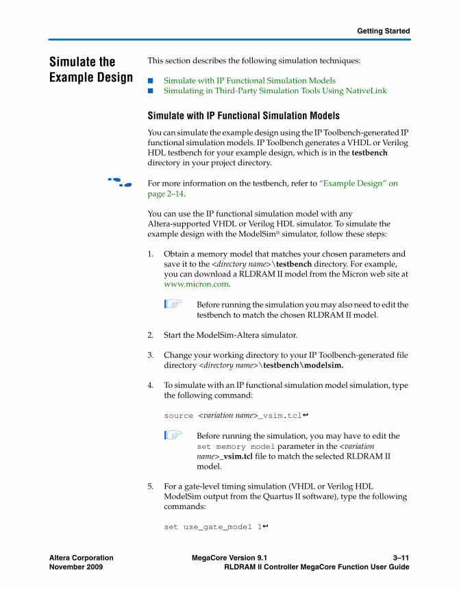
Getting Started
Simulate the Example Design
This section describes the following simulation techniques:
■ Simulate with IP Functional Simulation Models■ Simulating in Third-Party Simulation Tools Using NativeLink
Simulate with IP Functional Simulation Models
You can simulate the example design using the IP Toolbench-generated IP functional simulation models. IP Toolbench generates a VHDL or Verilog HDL testbench for your example design, which is in the testbench directory in your project directory.
f For more information on the testbench, refer to “Example Design” on page 2–14.
You can use the IP functional simulation model with any Altera-supported VHDL or Verilog HDL simulator. To simulate the example design with the ModelSim® simulator, follow these steps:
1. Obtain a memory model that matches your chosen parameters and save it to the <directory name>\testbench directory. For example, you can download a RLDRAM II model from the Micron web site at www.micron.com.
1 Before running the simulation you may also need to edit the testbench to match the chosen RLDRAM II model.
2. Start the ModelSim-Altera simulator.
3. Change your working directory to your IP Toolbench-generated file directory <directory name>\testbench\modelsim.
4. To simulate with an IP functional simulation model simulation, type the following command:
source <variation name>_vsim.tclr
1 Before running the simulation, you may have to edit the set memory model parameter in the <variation name>_vsim.tcl file to match the selected RLDRAM II model.
5. For a gate-level timing simulation (VHDL or Verilog HDL ModelSim output from the Quartus II software), type the following commands:
set use_gate_model 1r
Altera Corporation MegaCore Version 9.1 3–11November 2009 RLDRAM II Controller MegaCore Function User Guide
Simulate the Example Design
source <variation name>_vsim.tclr
Simulating in Third-Party Simulation Tools Using NativeLink
You can perform a simulation in a third-party simulation tool from within the Quartus II software, using NativeLink.
f For more information on NativeLink, refer to the Simulating Altera IP in Third-Party Simulation Tools chapter in volume 3 of the Quartus II Handbook.
To set up simulation in the Quartus II software using NativeLink, follow these steps:
1. Create a custom variation with an IP functional simulation model.
2. Obtain and copy an RLDRAM II model to a suitable location, for example, the testbench directory.
1 Before running the simulation you may also need to edit the testbench to match the chosen RLDRAM II model.
3. Check that the absolute path to your third-party simulator executable is set. On the Tools menu click Options and select EDA Tools Options.
4. On the Processing menu, point to Start and click Start Analysis & Elaboration.
5. On the Assignments menu click Settings, expand EDA Tool Settings and select Simulation. Select a simulator under Tool Name and in NativeLink Settings, select Compile Test Bench and click Test Benches.
6. Click New.
7. Enter a name for the Test bench name.
8. Enter the name of the automatically generated testbench, <project name>_tb, in Test bench entity.
9. Enter the name of the top-level instance in Instance.
10. Change Run for to 80 s.
3–12 MegaCore Version 9.1 Altera CorporationRLDRAM II Controller MegaCore Function User Guide November 2009

Getting Started
11. Add the testbench files. In the File name field browse to the location of the RLDRAM II model and the testbench, <project name>_tb, click OK and click Add.
12. Click OK.
13. Click OK.
14. On the Tools menu point to EDA Simulation Tool and click Run EDA RTL Simulation.
Edit the PLL The IP Toolbench-generated example design includes a PLL, which has an input to output clock ratio of 1:1 and a clock frequency that you entered in IP Toolbench. In addition, IP Toolbench correctly sets all the phase offsets of all the relevant clock outputs for your design. You can edit the PLL input clock to make it conform to your system requirements. If you re-run IP Toolbench and wish to save your PLL edits, turn off Update example design system PLL.
1 If you turn off Enable DQS mode, IP Toolbench generates a second PLL—the fedback PLL. You need not edit the fedback PLL.
f For more information on the PLL, refer to “PLL Configuration” on page 2–12.
To edit the example PLL, follow these steps:
1. Choose MegaWizard Plug-In Manager (Tools menu).
2. Select Edit an existing custom megafunction variation and click Next.
3. In your Quartus II project directory, for VHDL choose rldramii_pll_<device name>.vhd; for Verilog HDL choose rldramii_pll_<device name>.v.
4. Click Next.
5. Edit the PLL parameters in the altpll MegaWizard Plug-In.
f For more information on the altpll megafunction, refer to the Quartus II Help or click Documentation in the ALTPLL MegaWizard Plug-In.
Altera Corporation MegaCore Version 9.1 3–13November 2009 RLDRAM II Controller MegaCore Function User Guide

Compile the Example Design
Compile the Example Design
Before the Quartus II software compiles the example design it runs the IP Toolbench-generated Tcl constraints script, auto_add_rldramii_constraints.tcl, which calls the add_constraints_for_<variation name>.tcl script for each variation in your design. The add_constraints_for_<variation name>.tcl script checks for any previously added constraints, removes them, and then adds constraints for that variation.
The constraints script analyzes and elaborates your design, to automatically extract the hierarchy to your variation. To prevent the constraints script analyzing and elaborating your design, turn on Enable Hierarchy Control in the wizard, and enter the correct hierarchy path to your datapath (refer to step 13 on page 3–6).
When the constraints script runs, it creates another script, remove_constraints_for_<variation name>.tcl, which you can use to remove the constraints from your design.
To compile the example instance, follow these steps:
1. Choose Start Compilation (Processing menu), which runs the add constraints scripts, compiles the example design, and performs timing analysis.
2. View the Timing Analyzer to verify your design meets timing.
If the compilation does not reach the frequency requirements, follow these steps:
1. Choose Settings (Assignments menu).
2. Expand Analysis and Synthesis Settings in the category list.
3. Select Speed in Optimization Technique.
4. Expand Fitter Settings.
5. Turn on Optimize Hold Timing and select All Paths.
6. Turn on Fast-corner timing.
7. Click OK.
8. Re-compile the example design by choosing Start Compilation (Processing menu).
3–14 MegaCore Version 9.1 Altera CorporationRLDRAM II Controller MegaCore Function User Guide November 2009

Getting Started
1 To achieve a higher frequency, increase the number of address and command and write data pipeline registers, or increase the number read data pipeline registers, refer to step 6 on page 3–5.
To view the constraints in the Quartus II Assignment Editor, choose Assignment Editor (Assignments menu).
1 If you have “?” characters in the Quartus II Assignment Editor, the Quartus II software cannot find the entity to which it is applying the constraints, probably because of a hierarchy mismatch. Either edit the constraints script, or enter the correct hierarchy path in the Project Settings tab (refer to step 13 on page 3–6).
f For more information on constraints, refer to “Constraints” on page 2–16.
Program a Device
After you have compiled the example design, you can perform gate-level simulation (refer to “Simulate the Example Design” on page 3–11) or program your targeted Altera device to verify the example design in hardware.
With Altera's free OpenCore Plus evaluation feature, you can evaluate the RLDRAM II Controller MegaCore function before you obtain a license. OpenCore Plus evaluation allows you to generate an IP functional simulation model, and produce a time-limited programming file.
f For more information on OpenCore Plus hardware evaluation using the RLDRAM II Controller MegaCore function, refer to “OpenCore Plus Evaluation” on page 1–4, “OpenCore Plus Time-Out Behavior” on page 2–12, and AN 320: OpenCore Plus Evaluation of Megafunctions.
Implement Your Design
In the MegaWizard flow, to implement your design based on the example design, replace the example driver in the example design with your own logic.
1 A FIFO buffer is not implemented in the core; you must implement a FIFO buffer.
Set Up Licensing You need to obtain a license for the MegaCore function only when you are completely satisfied with its functionality and performance, and want to take your design to production.
Altera Corporation MegaCore Version 9.1 3–15November 2009 RLDRAM II Controller MegaCore Function User Guide

Set Up Licensing
After you obtain a license for RLDRAM II controller, you can request a license file from the Altera web site at www.altera.com/licensing and install it on your computer. When you request a license file, Altera emails you a license.dat file. If you do not have Internet access, contact your local Altera representative.
3–16 MegaCore Version 9.1 Altera CorporationRLDRAM II Controller MegaCore Function User Guide November 2009

Altera Corporation M
Additional Information
Revision History The table below displays the revision history for the chapters in this user guide.
How to Contact Altera
For the most up-to-date information about Altera products, refer to the following table.
Date Version Changes Made
November 2009 9.1 Updated the release information.
March 2009 9.0 Updated the release information.
November 2008 8.1 Updated the release information.
May 2008 8.0 ● Added timing assignment information for capture to first level resyncronization registers
● Registers clocked by DQS in the core now use undelayed DQS
May 2007 7.1 No changes.
March 2007 7.0 No changes.
December 2006 6.1 ● Added timing assignment information for 18 and 36-bit RLDRAM II devices● Updated device initialization sequence
April 2006 1.1.0 Updated format.
October 2005 1.0.0 First published.
Information Type Contact Note (1)
Technical support www.altera.com/mysupport/
Technical training www.altera.com/training/
Technical training services [email protected]
Product literature www.altera.com/literature
FTP site ftp.altera.com
Note to table:(1) You can also contact your local Altera sales office or sales representative.
egaCore Version 9.1 iRLDRAM II Controller MegaCore Function User Guide
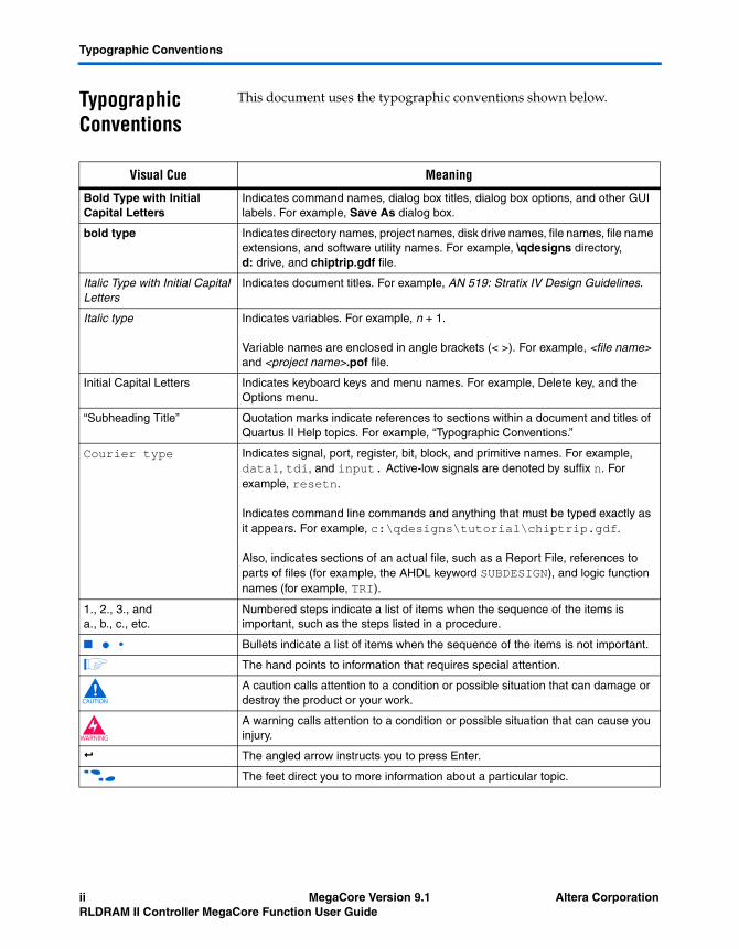
Typographic Conventions
Typographic Conventions
This document uses the typographic conventions shown below.
Visual Cue Meaning
Bold Type with Initial Capital Letters
Indicates command names, dialog box titles, dialog box options, and other GUI labels. For example, Save As dialog box.
bold type Indicates directory names, project names, disk drive names, file names, file name extensions, and software utility names. For example, \qdesigns directory, d: drive, and chiptrip.gdf file.
Italic Type with Initial Capital Letters
Indicates document titles. For example, AN 519: Stratix IV Design Guidelines.
Italic type Indicates variables. For example, n + 1.
Variable names are enclosed in angle brackets (< >). For example, <file name> and <project name>.pof file.
Initial Capital Letters Indicates keyboard keys and menu names. For example, Delete key, and the Options menu.
“Subheading Title” Quotation marks indicate references to sections within a document and titles of Quartus II Help topics. For example, “Typographic Conventions.”
Courier type Indicates signal, port, register, bit, block, and primitive names. For example, data1, tdi, and input. Active-low signals are denoted by suffix n. For example, resetn.
Indicates command line commands and anything that must be typed exactly as it appears. For example, c:\qdesigns\tutorial\chiptrip.gdf.
Also, indicates sections of an actual file, such as a Report File, references to parts of files (for example, the AHDL keyword SUBDESIGN), and logic function names (for example, TRI).
1., 2., 3., anda., b., c., etc.
Numbered steps indicate a list of items when the sequence of the items is important, such as the steps listed in a procedure.
■ ● • Bullets indicate a list of items when the sequence of the items is not important.
1 The hand points to information that requires special attention.
c A caution calls attention to a condition or possible situation that can damage or destroy the product or your work.
w A warning calls attention to a condition or possible situation that can cause you injury.
r The angled arrow instructs you to press Enter.
f The feet direct you to more information about a particular topic.
ii MegaCore Version 9.1 Altera CorporationRLDRAM II Controller MegaCore Function User Guide