
RJ 1.1 Receiver Construction Manual - Project Radio Jove - Nasa
50
1 JOVE RJ1.1 Receiver Kit Assembly Manual 2012 Receiver Kit and Manual developed for NASA JOVE Project by Richard S. Flagg, RF Associates [email protected]
Transcript of RJ 1.1 Receiver Construction Manual - Project Radio Jove - Nasa

1
JOVE RJ1.1 Receiver Kit
Assembly Manual
2012
Receiver Kit and Manual
developed for NASA JOVE Project
by
Richard S. Flagg, RF Associates

2
This page intentionally left blank.

3
Contents
Theory of Operation ............................................................................. 5
Components........................................................................................... 8
Circuit Diagrams................................................................................... 11
Tools .................................................................................................... 16
Soldering .............................................................................................. 17
The Work Area .................................................................................... 17
Identifying Parts ................................................................................... 17
Wiring the PC Board ........................................................................... 23
Assembly of the Enclosure.................................................................. 27
Testing and Alignment ......................................................................... 34
Troubleshooting ................................................................................... 43
Appendix A: Soldering Techniques ...................................................... 48
Appendix B: Resistor Color Code ........................................................ 49
Appendix C: Receiver Specifications ................................................... 50

4
This page intentionally left blank.

5
Radio JOVE
You are about to embark on building a short-wave receiver which will pick-up
radio signals from the planet Jupiter and also from the Sun. This receiver contains
over 100 electronic components and pieces of hardware. Fabrication will include
the handling of small, delicate, electronic parts, most of which will be mounted and
soldered on a printed circuit (PC) board.
The radio uses many different types of electronic components, with each part
performing a different job. However, before discussing these components and
what they do, we will look at the overall receiver (depicted in the block diagram in
Figure 1).
CONSTRUCTION TIME ESTIMATES
Part Identification approx. 1 hr.
Receiver Construction approx. 9 hrs.
Testing and Alignment approx. 1 hr.
Total Time approx. 11 hrs.
THEORY OF OPERATION
Radio signals from Jupiter are very weak - they produce less than a millionth of a
volt (1 microvolt, 1 v) at the antenna terminals of the receiver. These weak radio
frequency (RF) signals must be amplified by the receiver and converted to audio
signals of sufficient strength to drive headphones or a loudspeaker. The receiver
also serves as a narrow filter, tuned to a specific frequency to hear Jupiter while at
the same time blocking out strong earth based radio stations on other frequencies.
The receiver and its accompanying antenna are designed to operate over a narrow
range of short-wave frequencies centered on 20.1 MHz (megahertz). This
frequency range is optimum for hearing Jupiter signals.
Antenna The antenna intercepts weak electromagnetic waves which have traveled some 500
million miles from Jupiter to the Earth. When these electromagnetic waves strike
the wire antenna, a tiny RF voltage is developed at the antenna terminals. Signals
from the antenna are delivered to the antenna terminals of the receiver by a coaxial
transmission line.

6
RF Bandpass Filter and Preamplifier Signals from the antenna are filtered to reject strong out-of-band interference and
are then amplified using a junction field effect transistor (JFET). This transistor
and its associated circuitry provide additional filtering and amplify incoming
signals by a factor of 10. The receiver input circuit is designed to efficiently
transfer power from the antenna to the receiver while developing a minimum of
noise within the receiver itself.
Local Oscillator and Mixer The local oscillator (LO) and mixer perform the important task of converting the
desired radio frequency signals down to the range of audio frequencies. The local
oscillator generates a sinusoidal voltage wave form at a frequency in the vicinity of
20.1 MHz. The exact frequency is set by the front panel tuning control. Both the
amplified RF signal from the antenna and the LO frequency are fed into the mixer.
The mixer develops a new signal which is the arithmetic difference between the
LO and the incoming signal frequency. Suppose the desired signal is at 20.101
MHz and the LO is tuned to 20.100 MHz. The difference frequency is therefore
20.101-20.100 = .001 MHz, which is the audio frequency of 1 kilohertz. If a signal
were at 20.010 MHz it would be converted to an audio frequency of 10 kHz. Since
the RF signal is converted directly to audio, the radio is known as a direct
conversion receiver.
Low Pass Filter
To eliminate interfering stations at nearby frequencies, we use a filter which is like
a window a few kilohertz wide through which Jupiter signals can enter. When
listening for Jupiter or the Sun, the radio will be tuned to find a “clear channel.”
Since frequencies more than a few kilohertz away from the center frequency may
contain interfering signals, these higher frequencies must be eliminated. This is
the purpose of the low pass filter following the mixer. It passes low (audio)
frequencies up to about 3.5 kHz and attenuates higher frequencies.
Audio Amplifiers The purpose of the audio amplifiers following the low-pass filter is to take the very
weak audio signal from the mixer and amplify it enough to drive headphones
directly, or to drive an external amplified speaker assembly.

7
Figure 1. JOVE receiver block diagram
Antenna
RF Bandpass Filter
RF Preamp J310
LO / Mixer NE 602
5 Pole Low Pass Filter
Audio Preamp LM387
Audio Amp
External Amplified Speaker
20.00 MHz Test Oscillator
Tuning
(20.1 MHz +/- 150 kHz)
Volume
Audio Out 2
Audio Out 1

8
COMPONENTS
The JOVE receiver uses many different electronic components (Figure 2)
including wires, resistors, capacitors, inductors, diodes, transistors and integrated
circuits. Each performs different functions.
Wires are made of conducting metal—they direct the flow of electrical current
from one place to another. Since wire is a good conductor, it has a low resistance
to the flow of electricity. The printed circuit (PC) board used in this kit uses traces
of copper etched on an insulating fiberglass back plane in place of individual
wires.
Resistors conduct electrical current, but they are designed to impede the flow of
electrons. This characteristic of resistance limits the amount of current flow
according to Ohm’s law. Resistors dissipate electrical power by generating heat.
The value of a resistor is given in Ohms ( ), while its maximum power dissipation
is given in watts. There are fixed resistors and variable resistors. Two variable
resistors are used in this kit—one as the volume control and the other as the tuning
control. The fixed resistors in this kit have several different values of resistance,
but they are all 1/4 watt size. See Appendix B for reading resistor value color
codes.
Capacitors appear as an open circuit to direct current (DC) but pass audio and
radio frequency signals. The value of a capacitor is given in Farads (F), although it
is most common to use capacitors with values in the range of microFarads ( F) or
picoFarads (pF). Since the capacitor is physically made of two conducting plates
separated by a very thin layer of insulation it is possible for an electrical voltage to
arc between the plates and destroy the capacitor. For this reason capacitors have a
maximum voltage rating. Capacitors store energy in the electrical field between
the plates but do not dissipate power like resistors.
Inductors are simply coils of wire which pass direct current and have the property
of resisting changes in current flow. The value of inductance is the Henry (H),
although it is most common to use coils whose inductance is measured in
milliHenries (mH), or microHenries ( H). Inductors store energy in the magnetic
field surrounding the coil. When inductors and capacitors are used together they
form a resonant circuit which swaps energy between the magnetic field of the

9
Figure 2. Components
A
B
C
D
E
F
G
B
A
C
Resistors
A – Variable Resistor (Tuning
Control)
B – Fixed Resistors
A
B
Capacitors D – Disc Ceramic
A – Metal Polyester E – Dipped Ceramic
B – Electrolytic F – Tantalum
C – Metal Film G – Variable Capacitor
Inductors
A – Variable Inductor (silver can)
B – Fixed Inductor
C – Fixed Inductor (black cylinder)

10
Figure 2. Components, continued
Solid State Devices
A – Diode 1N4001
B – Diode 1N914
C – Transistor 2N-3906
D – Varactor Diode MV-209
E – Integrated Circuit SA-602
F – Oscillator Module
Connectors and Hardware
C – 2.1 mm Power Connector
A – Solder Lug D – 3.5 mm Stereo Audio Jack
B – Spacer E – Chassis Coaxial Connector
Ground Resistor Inductor Capacitor Transistor Diode
Variable Variable Variable Schematic Resistor Inductor Capacitor Battery Symbols
C
D
E
F
A
B
A
B
C
D
E

11
inductor and the electric field of the capacitor. This has the effect of forming a
resonant circuit - which is tuned to a certain audio or radio frequency - much as an
organ pipe is resonant at a particular audio frequency. Such a circuit acts like a
filter - selecting only a narrow range of desired frequencies and rejecting others.
Resonant circuits often use variable capacitors or variable inductors which must be
adjusted for optimum performance at the desired frequency.
Resistors, capacitors, and inductors are used to route signals and DC voltages
within a circuit and to select or reject certain frequencies by filtering. Certain
capacitors (electrolytic type) have a (+) and (-) terminal and must be installed with
the proper orientation in a circuit. Resistors, inductors, and non-electrolytic
capacitors may be installed in any orientation.
Diodes are solid state devices which allow current flow in one direction only. The
diode has an anode (+) and a cathode (-) and must be installed with the proper
orientation.
Transistors are generally three—terminal solid state devices used to amplify
signals. Bipolar transistor terminals are known as the base (b), emitter (e), and
collector (c). A small signal injected into the base will appear amplified at the
collector. Another type of transistor is the field effect transistor (FET). The
terminals of this device are known as the gate (g), source (s), and drain (d). The
transistor requires power to amplify signals so there is always a connection to a
source of DC power.
Integrated Circuits are often made up of hundreds of transistors, diodes, and
resistors all interconnected to perform specific functions. This kit uses three
integrated circuits (ICs), each with 8 pins. The orientation of the IC in the circuit
is important as each pin has a different use.
CIRCUIT DIAGRAMS
We have already seen a block diagram of the JOVE receiver, which shows the
radio as a group of functional blocks connected together. While this type of
diagram does not show individual components like resistors and capacitors, it is
useful in understanding signal flow and the various functions performed within the
radio.
The next level of detail is the schematic diagram. A schematic is used to represent
the wiring connections between all of the components which make up a circuit.

12
The schematic diagram uses symbols for each of the different components rather
than pictures of what the components actually look like. The symbols and pictures
of several of the components used in this kit are seen in Figure 2. A schematic
diagram of the complete receiver is seen in Figure 3. On this schematic, the part
types are numbered sequentially. For example, inductors are denoted L1 through
L7, and resistors are denoted R1 through R31.
Signal flow as shown in the schematic is as follows. The signal from the antenna
connector (J2) is coupled to a resonant circuit (bandpass filter L1, C2, C3) and then
to the J-310 transistor (Q1), where it is amplified. The output of the J-310 goes
through another resonant filter (L3, C6) before being applied to the resonant input
circuit (L4, C9, C10) of the SA602 integrated circuit (IC1), which serves as the
local oscillator and mixer. The center frequency of the local oscillator is set by
inductor L5 and adjusted by the tuning control R7. The audio output from IC1
passes through the low-pass audio filter (L6, L7, C20, C21, and C22). The audio
signal is next amplified by IC2 (an LM387) before going to the volume control
R15. The final audio amplifier stages comprise IC3 (another LM387), and the
output transistors Q2 (2N-3904) and Q3 (2N-3906). After the receiver has been
assembled, the variable capacitors C2 and C6 and variable inductors L4 and L5
will be adjusted to tune the receiver for operation at 20.1 MHz.
Another useful representation of the circuit is a PC board layout diagram (Figure
4). This is a pictorial representation showing the actual parts placement on the
printed circuit board. This X-ray view from the component side of the board
shows the components as rectangles or circles, and the trace side of the board as
faint gray areas. A similar PC layout diagram (Figure 5) just shows the
components, without the X-ray view of the traces. This view of the components is
identical to the component outlines marked on the actual PC board
An exploded view (Figure 7) shows the PC board and the enclosure, with
connectors and controls mounted on the front and rear panels of the box.

13
Figure 3. Schematic diagram
IC1
-SA
602
IC2
– L
M38
7
IC3
– L
M38
7

14
Figure 4. X-ray view of PC board from component side
LM387
LM387
SA
602

15
Figure 5. PC board - component side
LM387
LM387
33 k
3-2
0p
F
SA
602

16
The parts list (Table 1) identifies each component by its value and part number.
As you begin construction the first step will be to identify each component and
check it off on the parts list to make sure that you have received all of the parts.
This table is an important link between the bag of parts which you have received
and installing those components in the right place in the radio as shown by Figures
4, 5, and 6.
Although this is a complicated project, it can be built successfully. You are urged
to take great care to install the right parts in the right places on the PC board.
Before soldering make sure you have the right component. Also be sure the
orientation is correct—electrolytic capacitors, transistors, integrated circuits and
diodes must be installed with the correct orientation.
TOOLS
(Radio Shack parts numbers follow many of the items)
Soldering Iron (RS 64-2071; 40 Watt) or or 40-Watt Weller WLC100 or
Velleman 50W Soldering Station (part # VTSS5U; check Amazon.com) [NOTE: A small wattage soldering iron or soldering pencil (25-30 watts) is ideal for building the
receiver but is not big enough for the larger wires and joints in the antenna. A 50 watt soldering
iron, or a higher wattage (100-150 watts) soldering gun is best for the antenna, although if you
are patient you may get by with a 40 watt iron (make sure the solder flows throughout the wire
strands). A variable wattage iron (25-50 watts) like the Velleman 50W Soldering Station is
recommended since it can be used for both the receiver and antenna. If you purchase a simple
soldering iron with no stand, please obtain a stand to hold the hot iron. Another advantage of
purchasing a soldering station is that it includes a stand for the hot iron. Whatever soldering
equipment you purchase clean and tin the tip frequently for best performance.]
Solder, rosin core 60/40 (.050 in., RS64-006 or .032 in., RS 64-005)
Wire Cutters and Wire Strippers (RS 64-080 Wire Stripper and Nippy Cutter)
Diagonal Cutters, 5 inch Nippy Cutter (RS 640-0064)
Long Nose Pliers (RS 640-0062)
Phillips screwdriver (with small tip)
Small Crescent wrench or 3/8” and 7/16” open wrenches
*Allen wrench (hex) 1/16 inch
*Sandpaper
*Plastic tool for adjusting variable inductors
*Plastic tool for adjusting variable capacitors
* These tools are included with the kit

17
SOLDERING
Key to successful fabrication of this JOVE receiver kit is your ability to solder. It
is important that each solder joint be made correctly—heating the joint so that the
solder flows and joins the component lead to the solder pad, without applying so
much heat that the component is damaged. See Appendix A for a guide to good
soldering techniques, or see our videos Online:
http://radiojove.gsfc.nasa.gov/telescope/soldering.htm.
THE WORK AREA
Select a work area with good light and an electrical outlet. The area should be
large enough for a comfortable work space for a couple of people, a soldering iron,
tools, the instruction manual, and the kit parts. Keep the work space clean so parts
don’t get lost.
IDENTIFYING PARTS
Check the parts you have received against the list in Table 1 (JOVE Parts List).
With the aid of the capacitor sorting sheet, Figure 2, and appendix B, make
absolutely sure you have identified each part correctly. Each part in the kit has a
designation (for example resistor R1, or capacitor C21). Each part has a
manufacturers designation printed on the part as to the value of the part. Resistor
values are designated by colored bands (see appendix B). Capacitor designations
are more complex and often contain “too much” information – such as
manufacturers date codes and lot numbers.
Ceramic Capacitors often have numbers and letters on both sides. In the parts list
we show only the information printed on the “front side” of the capacitor – the side
that tells the value of the capacitor along with information related to the tolerance,
temperature stability and voltage. As an example, C1 which is a 39pf ceramic
capacitor, could have either 390/A1J or 39J printed on the front side (depending on
the manufacturer). The zero in 390 is a multiplier (10 to the zero power which is
1), so the value is 39pf. The letter J is for 5% tolerance.
Electrolytic capacitors usually have the the value in microfarads as well as a
maximum voltage rating. These caps are polarized – there is a positive and
negative lead. The long lead is positive (+).

18
There is a source of confusion in identifying several capacitors used in the Jove kit: capacitors are marked
on both the front and back side. The table below shows the front side and back side markings on the
capacitors that are currently being shipped with the Jove kits.
Designation Value Front Side Back Side Color
C4 22 pf 220
A1J
039
RCP
Orange
C1 39pf 39J 5A Blue
C3 56pf 560
A1J
039
RAS
Orange
C28 220pf 221
A1J
046
RFT
Orange
The problem is in identifying which side of the capacitor contains the correct value. Which side is the
“front side”?
Say you are looking for C1, which by proper convention should read 390. (The 0 at the end is a multiplier
– in this case 0 means 100 – which is a multiplier of 1). If you read the “back side” of the 22pf cap, you
would see 039/RCP and if you picked up the 56pf cap and read the “back side” you would read 039/RAS.
If you picked up the 39 pf cap and read the “front side” you would read 39J. Great – none of these caps
follows the normal convention—and worse yet, all three could be interpreted to be a 39 pf capacitor.
A careful look at the table above reveals that the front side (the correct side) to read for each
capacitor contains the letter J. The letter J means a tolerance of +/-5%.
In the figure below, the kit part number is shown—for example, C1—beside each capacitor.
Radio JOVE Receiver Kit — Capacitor Sorting and Identification (2012)

19
Table 1
JOVE Receiver Parts List
Actual marking found on component is shown in parentheses ( ). See capacitor
sorting sheet for reference. Two columns of check-off boxes are provided: use one
for parts identification, and the other, for installation.
CAPACITORS Note polarity on all electrolytic capacitors
C1 39 pF, ceramic (390/A1J or 39J)
C2 4-40 pF, variable (white)
C3 56 pF, ceramic (560/A1J or 56J)
C4 22 pF, ceramic (220/A1J or 22J)
C5 .01 F, ceramic (103)
C6 3-20 pF, variable (green)
C7 not used
C8 .01 F, ceramic (103)
C9 47 pF, ceramic (470/A1J or 47J)
C10 270 pF, ceramic (271/A1J)
C11 0.1 F, ceramic (104)
C12 47 pF, ceramic (470/A1J or 47J)
C13 47 pF, ceramic (470/A1J or 47J)
C14 0.1 F, ceramic (104)
C15 10 pF, ceramic (100/A1J or 10J)
C16 10 F, 25 vdc, electrolytic, long lead is +
C17 0.1 F, ceramic (104)
C18 0.1 F, ceramic (104)
C19 1 F, metal polyester (105K/100A)
C20 0.068 F, 5% metal film (18L/683)
C21 0.1 F, 5% metal film (17L/104)
C22 0.068 F, 5% metal film (18L/683)
C23 0.1 F, ceramic (104)
C24 10 F, 25 vdc, electrolytic, long lead is +
C25 10 F, 25 vdc, electrolytic, long lead is +
C26 0.1 F, ceramic (104)
C27 10 F, 35 vdc, tantalum, marked lead is +
C28 220pF, ceramic (221/A1J)
C29 0.1 F, ceramic (104)
C30 10 F, 25 vdc, electrolytic, long lead is +

20
C31 10 F, 25 vdc, electrolytic, long lead is +
C32 330 F, 25 vdc, electrolytic, long lead is +
C33 10 F, 25 vdc, electrolytic, long lead is +
C34 0.1 F, ceramic (104)
C35 0.1 F, ceramic (104)
C36 0.1 F, ceramic (104)
C37 10 pF, ceramic (100/A1J or 10J)
C38 10 F, 25 vdc electrolytic, long lead is +
C39 100 F, 25 vdc electrolytic, long lead is +
C40 0.1 F, ceramic (104)
C41 0.1 F, ceramic (104)
C42 0.1 F, ceramic (104)
C43 0.1 F, ceramic (104)
C44 10 F, 25 vdc electrolytic, long lead is +
DIODES Note polarity
D1 1N4001
D2 1N914
D3 1N914
LED1 light emitting diode (LED), red, long lead is +
VD1 MV209, varactor diode
ZD1 1N753, 6.2 v, zener diode, 400 mw
ZD2 1N5231, 5.1v, zener diode, 500mw
INDUCTORS Do Not Confuse L1, L2, L3 with Resistors
L1 0.47 H, (yellow, violet, silver, silver)
L2 1 H, (brown, black, gold, gold)
L3 3.9 H, (orange, white, gold, gold)
L4 1.5 H, adjustable inductor, (silver can)
L5 1.5 H, adjustable inductor, (silver can)
L6 82 mH, fixed inductor, (black cylinder)
L7 82 mH, fixed inductor, (black cylinder)
INTEGRATED CIRCUITS
IC1 SA602AN, mixer / oscillator
IC2 LM387, audio preamplifier
IC3 LM387, audio preamplifier
OSC1 20.000 MHz crystal oscillator module

21
RESISTORS Some resistors have 4 color bands, and others
5; see Appendix B for help or use a ohmeter to
confirm resistance values
R1 68 ohm (blue, gray, black, gold)
R2 294 ohm (red, white, yellow, black, brown)
R3 17.4 ohm (brown, violet, yellow, gold, brown)
R4 294 ohm (red, white, yellow, black, brown)
R5 100 ohm (brown, black, black, black, brown)
R6 2.2 Kohm (red, red, red, gold)
R7 10 Kohm linear potentiometer
R8 2.2 Kohm (red, red, red, gold)
R9 100 Kohm (brown, black, yellow, gold)
R10 220 ohm (red, red, brown, gold)
R11 1.5 Kohm (brown, green, red, gold)
R12 1 Kohm (brown, black, red, gold)
R13 27 Kohm (red, violet, orange, gold)
R14 33 Kohm (orange, orange, orange, gold)
R15 10 Kohm potentiometer /switch
R16 10 Kohm (brown, black, black, red, brown) or
(brown, black, orange, gold)
R17 1.5 Kohm (brown, green, red, gold)
R18 27 Kohm (red, violet, orange, gold)
R19 100 Kohm (brown, black, yellow)
R20 1 Kohm (brown, black, red, gold)
R21 1 Kohm (brown, black, red, gold)
R22 2 ohm (red, black, gold)
R23 2 ohm (red, black, gold)
R24 1 ohm (brown, black, gold)
R25 220 ohm (red, red, brown, gold)
R26 51 ohm (green, brown, black, gold)
R27 1Kohm (brown, black, red, gold)
R28 10 ohm (brown, black, black, gold)
R29 10 ohm (brown, black, black, gold)
R30 10 ohm (brown, black, black, gold)
R31 10 ohm (brown, black, black, gold)
R32 51 ohm (green, brown, black, gold)

22
TRANSISTORS
Q1 J-310, junction field effect, (JFET)
Q2 2N-3904, bipolar, NPN
Q3 2N-3906, bipolar, PNP
HARDWARE/MISC
E1 Enclosure 5x7x2
PCB1 Printed Circuit Board
J1 Power Jack, 2.1 mm
J2 F female chassis connector
J3 3.5 mm stereo jack, open ckt
J4 3.5 mm stereo jack, open ckt
spacers (2) 0.375 inch spacer, 4-40 thread
K1, K2 Knob, 1/8 inch shaft
P1 2.1 mm plug with 72 inch cord
Screw (5) 4-40 thread, 1/4 inch long
Lock washer (5) #4
Flat washer (2) #4
Nut (1) 4-40
Solder Lug(1) #4
Wire 6 in. red and 6 in. black and 18 in. bare wire
Feet (4) Rubber adhesive feet
OTHER MATERIALS
Allen Wrench 1/16 inch for knobs
Sandpaper
Tuning tool White – for tuning inductors L4, L5
Tuning tool Black – For tuning capacitors C2 and C6
AC Adapter Jameco 12 volt power adapter (500mA) *Only
included for USA, Mexico, and Canada orders*
NOTE: Be careful about the orientation of the IC components – make sure to
read and pay attention to the installation directions starting on page 23.

23
WIRING THE PC BOARD
The PC board will be populated in an order that will give you a chance to sharpen
your soldering skills. You will install simple resistors and capacitors first, before
getting to the transistors and integrated circuits which may be damaged by excess
heat.
Mounting the Components Mount the components as close to the board as possible without putting excessive
strain on the leads. Some component lead spacings will match the board hole
spacing and the component will mount flush with the board. In other cases, the
component leads must be formed to align with the holes. Hold the component
body in your fingers and form the leads with the needle nose pliers. Don’t grasp
the component with the pliers.
Figure 6. Forming the component leads to match up with PC board hole spacings
When forming the leads of the small ceramic capacitors leave at least 1/16 inch
between the body of the capacitor and any bends. The capacitor body may fracture
if the leads are overstressed.
When forming the leads of transistors always make bends farther than 1/8 inch
from the transistor body. Some transistor leads show a crimp mark, near the
transistor body. Never bend leads closer to the transistor than this crimp mark..
When you are cutting leads, shield the cut with your hand, or aim the work down,
to prevent the cut wire from flying into someone’s face.

24
Be very careful to use the correct component values. It’s a lot easier to double
check before soldering, than it is to have to unsolder and replace a part. Refer to
Appendix A for soldering techniques.
After each component is soldered-in, make a check mark on the parts list (Table 1)
and the PC parts layout diagram (Figure 5). As you go through the assembly
procedure put a check mark in each after completing the step. Several
photographs of the completed PC board are included near the end of the manual
(Figure 20).
The following assembly sequence is recommended. Read each step completely
before performing that step. See Figure 2 and the capacitor sorting sheet for parts
identification.
The term “install” means to identify the part, form the leads, insert the component
leads in the PC board, solder, and trim away the excess lead.
1. Inspect the PC board by looking at it from the component side while holding
it up to a light. Compare traces and hole patterns with Figure 4 in this
manual, making sure that all holes are drilled and that the trace patterns
match.
2. Using the bare wire in the main parts bag and needle nose pliers, install the
jumper wires J1 through J10. A simple way to do this is to (1) thread the two
holes for the jumper wire with the long piece of wire, (2) allow about ¼ in.
extra out the bottom of the holes, (3) bend the wire to hold it into place, (4)
snip off the long excess wire. Repeat this for all jumper wires and the long
wire gets progressively shorter. Solder all jumper wires into place, and cut
off any excess wire.
3. Install fixed resistors R1 through R27. You can do this one resistor at a time,
or you may prefer to insert several resistors (spreading the leads slightly on
the trace side of the board to hold the resistors in place) and then soldering
several resistors. Don’t insert all the resistors before soldering, or you will
have a forest of leads that will interfere with soldering. Small groups of half
a dozen or so will work well. While soldering, you can lay the PC board on a
flat surface to help hold the resistors in place.
4. Install inductors, L1, L2, and L3. See Figure 2 for parts identification

25
5. Install the three IC sockets. Each socket has a small notch in one end. The
socket must be mounted so that the notch is near the pin 1 dot on the IC
outline printed on the component side of the PC board. Insert the socket pins
into the PC board and place the board on a flat surface so the socket is
pushed flush against the board. Solder one pin, and check to see that the
socket is flush with the board before soldering the remaining pins.
6. Install fourteen 0.1 F dipped ceramic capacitors. [C11, C14, C17, C18,
C23, C26, C29, C34, C35, C36, C40, C41, C42, C43] These capacitors are
not polarized and can be installed in either orientation.
7a. Install eight 10 F, 25vdc electrolytic capacitors, [C16, C24, C25, C30, C31,
C33, C38, and C44]. Carefully observe the polarity and proper orientation.
Each capacitor has a vertical band with minus signs running from top to
bottom along one side. The lead nearest this band is the negative lead of the
capacitor. The PC board is marked with small + signs denoting the correct
placement of the + lead for each electrolytic capacitor. The + lead is the
long lead.
7b. Install C32, C39. Note that the positive (+) leads are long.
8. Install C27, then install remaining capacitors. Note that the tantalum leads of
C27 are equal length. The + lead is marked on the body.
9. Install inductors, L4, L5, L6, and L7. Solder all pins and mounting tabs on
L4 and L5.
10. Install the tuning control potentiometer (variable resistor R7), and the audio
gain potentiometer / on-off switch (R15/S1). Solder one pin and then check
to make sure that the part is properly aligned and seated before soldering the
remaining pins. Make sure that the solder pins are fully seated in the PC
board holes and that the control shafts are parallel to the plane of the PC
board.
11. Install transistors, Q1-Q3. Note the orientation (see Fig. 4 or 5).
12. Install diodes D1, D2, D3, VD1, ZD1, and ZD2. Note the orientation. The
band on the diode must match up with the band marked on the PC board.

26
13. Install the test oscillator OSC1. Note three of the four corners are beveled
while the corner near pin 1 is square. The PC board shows the orientation of
OSC1 by denoting pin 1 as the square corner.
14. Install one end of each fixed resistor R28-R31 on the PC board. Leave
about ¼ inch of lead between each resistor and the board. The other end of
each resistor will be soldered later to the audio jacks (see Figure 13).
15. Plug the integrated circuits (ICs) into their sockets. The IC must be plugged
into the socket with the pin 1 mark (usually a small dimple or circle in the
corner of the IC case) near the notch in the socket. Be careful inserting the
IC into the socket – it is easy to have one pin fold up under the IC. The
easiest way is to register the IC pins along one side of the socket so that they
are just inside the socket holes. Then using your fingernail, or a flat object
like a screwdriver blade – push the IC pins on the opposite side inward until
they align with the socket holes. Once all the pins are aligned, push down
firmly until the IC seats completely in the socket. All the pins should be in
the same depth. If you accidentally bend one of the IC pins, remove the IC
from the socket (by inserting a thin blade under the IC and gently prying up)
and carefully straighten the IC pin before reinserting into the socket. When
removing an IC from the socket, pry a little on one end, and then switch to
the other end. Use caution as you pull the IC out of the socket – it is easy to
end up with the IC plugged into your finger!
16. Carefully examine every solder joint that you have made. If possible, use a
bright light and a magnifying glass. Most problems are caused by bad solder
joints. Look for solder bridges and joints that do not bond the component
lead to the PC board trace. Make sure that every component lead is soldered.
All solder joints should be bright and smooth. Make sure that there are no
cut wires stuck to the board. Double check the polarity and orientation of all
electrolytic capacitors, transistors, and diodes.
Note that the LED will be installed later.
This completes assembly of the PC board.
4
5
3
6 7
8
2 1

27
ASSEMBLY of the ENCLOSURE
The receiver enclosure comprises 6 aluminum plates, 4 lengths of extruded
channel, and 8 small Phillips screws. Panels have been pre-punched with holes for
controls, connectors and mounting screws. Plastic film covers the outside (visible
side) of each panel. The exploded view (Figure 7) shows how the panels will be
assembled in the following steps.
Figure 7. Exploded view of the enclosure and PC board

28
PREPARING the ENCLOSURE PANELS
1. Examine each enclosure panel. The front and rear panels have been screened
with labels and marking for convenience.
2. Using the supplied sandpaper (or a fine file), remove the sharp edges and
corners from each panel. Be careful not to mar or scratch the panel surface.
3. Mount the power connector, two audio jacks, the antenna connector, and a
solder lug to the rear panel (Figure 8). Power and audio connectors are passed
through the panel from the “inside” with washers and nuts located on the decal side
of the panel. The F-coax connector is inserted from the decal side with washer and
nut on the inside. Tighten the nuts firmly with a crescent wrench or pliers.
Figure 8. Rear panel assembly

29
WIRING the REAR PANEL
1. Prepare two 2 inch red wires and two 2 inch black wires by stripping 1/4
inch of insulation from both ends of each wire. Use a good wire stripping
tool to avoid cutting the wires. Twist the wire strands together and tin the
wires (heat with the soldering iron and apply a small amount of solder to
hold the strands together).
2. Install a red wire on the center pin of the antenna connector on the back
panel. Install a black wire on the solder lug adjacent to the antenna
connector on the back panel. Make a good mechanical joint before
soldering.
3. Solder resistor (R32) between the center pin of the antenna connector and
the adjacent solder lug. Use the minimum necessary lead length. This
resistor simulates the antenna during testing and will be removed after
testing and alignement.
4. Thread a bare wire through the ground tab of audio jack (J3) and solder one
end to the ground tab of J4. Also solder this wire to the ground tab of J3.
Insert the end of this bare wire into the top tab of the power connector but do
not solder (see Figure 9).
Figure 9. Rear panel wiring of power and audio connectors.
5. Attach the remaining 2” black wire to the top lug of the power connector
(inserting it into the same hole as the bare wire from J3) and solder. Make
sure that no wire strands of the black wire come in contact with the left-hand
lug of the power connector.
Bare Wire
PC Board
Black
Red
+12 vdc
J1 J3 J4
Ground Tabs
Bare Wire

30
6. Install the remaining 2” red wire to the left hand lug of the power connector.
Make sure that no wire strands of the red wire come in contact with the top
lug of the power connector.
MOUNTING the PC BOARD to the FRONT PANEL
1. Mount the PC board to the front panel. Simply slip the potentiometer shafts
through the front panel holes and apply the lock washers and nuts. Tighten
nuts.
2. Form the leads of LED1 and insert the LED into the front panel hole from
the rear such that the LED leads extend to the PC board mounting holes.
The longer of the LED leads goes in the + hole. Solder in place, then trim
the extra leads after soldering.
3. Install the two knobs. Align them so that when the control is turned full
counterclockwise, the index mark is near the 7 o’clock position (Figure 10).
Once the knob set screw is tightened down, the full counterclockwise
rotation and the full clockwise rotation of the knob index mark should be
equal-spaced from the 6 o’clock position.
Figure 10. Jove receiver front panel with knob alignment.
4. Install two spacers (Figure 11) below the rear corners of the PC board using
1/4 inch long, 4-40 screws and lock washers.
Figure 11. Spacers mounted to the bottom of the PC board
PC Board
Spacer

31
ASSEMBLE the ENCLOSURE
1. Partially assemble the enclosure using one end panel, the four extruded
channel pieces, and four screws. Tighten screws just enough to maintain
shape. See Figure 12.
Figure 12. Partial assembly of the enclosure.
2. Slide the front panel with the attached PC board into the front channel
guides, moving it back until it is flush with the side panel. If the panel gets
crooked in the guides it may jam and refuse to slide along the grooves. If the
panel jams, loosen the screws slightly.
3. Slide the rear panel into the rear channel guides, moving it back until it is
flush with the side panel. Be sure that the panel is installed “right side up.”
Bend the red and black wires on the power connector up so they do not hit
the components on the PC board.
4. Mount the right side panel to the four channel guides with four screws.
Tighten all 8 enclosure screws enough to maintain the enclosure shape. The
enclosure now includes the front panel, rear panel, and both side panels
supported by the channel guides.

32
5. Install the red wire attached to the center pin of the antenna connector to the
antenna hole on the PC board. Install the black wire attached to the solder
lug adjacent to the antenna connector on the back panel to the ground hole
on the PC board adjacent to the screw hole in the corner. The location of
these wires on the PC board is easily seen in the X-ray view (Figure 4).
6. Install the red wire from the power connector to the PC board hole labeled
+12 vdc (Figure 13). Install the black wire from the power connector to the
ground hole on the PC board adjacent to the screw hole in the corner. The
location of these wires on the PC board is easily seen in the X-ray view
(Figure 4).
7. Complete installation of resistors R28, R29, R30 and R31 as shown in
Figure 13. Leave a little extra lead length so that the resistor leads are not
taut. First solder R29 and R31 on the bottom tabs of the two audio
connectors. Then solder R28 and R30 to the top horizontal tabs as shown in
Figure 13. Trim excess lead wires after soldering.
Figure 13. Rear panel wiring (resistor R32 not shown)

33
Before installing the bottom panel make one more visual inspection of
the trace side of the PC board.
13. Remove the right side panel, slide in the bottom panel and attach it to the
spacers with 1/4 inch 4-40 screws, flat washers and lock washers (Figure
14). The bottom panel holes are not equidistant from the edges - the hole on
the TUNING control side is closer to the right edge than the hole on the
VOLUME control side is to the left edge. You may need to flip the bottom
panel if the holes do not line up with the spacers. Reattach the right side
panel. Attach the four rubber feet to the corners of the bottom panel. At this
point the enclosure is complete except for the top panel.
Figure 14. Mounting the spacers to the bottom panel

34
TESTING AND ALIGNMENT
Make a final visual check to be sure all transistors, integrated circuits, diodes and
electrolytic capacitors are properly installed – in the correct locations with the
right orientations. Before performing any of these procedures read through the
whole test section and get clearly in mind the steps which you plan to follow.
Power and Audio Connections
1. The receiver requires 12 volts DC which may be obtained from an AC
adapter, a well regulated power supply, or from a battery (Figures 15 and 16).
Current drain is approximately 60 milliamps (ma). The Jameco® AC adapter
(supplied with US orders) is the recommended power source for indoor use.
Switching power supplies are not recommended as many of these units generate
undesirable radio noise. A linear, regulated supply is preferred.
The kit is also supplied with a power cord that has a female plug on one end and
stripped leads on the other end. This cord can be used to power the Jove receiver
from a 12 volt regulated DC power supply or a 12 volt battery. Notice that the
cord has a colored stripe or tracer, along one of the wires. This is the wire that is
connected to the center conductor of the plug and must be connected to the (+) side
of the power source (Figure 15).
Figure 15. Wiring the power plug to a battery -
the colored tracer goes to the + side of the supply.
-
B la c k
T ra c e
Colored
Trace

35
2. Before connecting power turn the JOVE receiver power switch OFF.
Connect either headphones or an amplified speaker (Radio Shack 277-1008 or 40-
218, or equivalent) to one of the audio output jacks on the receiver rear panel.
These jacks accept 3.5 mm (1/8 inch) monaural or stereo plugs. Connect the JOVE
receiver to the 12 volt power source as shown in Figure 16. First connect the
power cord to the receiver and then plug the supply into the wall outlet. (It is not
recommended to plug a live power plug into the receiver.)
Figure 16. Test set-up, radio with the cover off
connected to the AC Adapter and the amplified speaker
3. If you are using an amplified speaker, turn it ON and adjust the volume
control on the speaker up about 1/8 turn. If you are using headphones, hold them
slightly away from you ear at first as there may be a loud whistle due to the
internal test oscillator when you turn the receiver on. Turn the JOVE receiver ON.
The front panel LED should light. Set the JOVE volume control to the 12 o’clock
position. Allow the receiver to “warm-up” for at least two minutes.
[NOTE: troubleshooting procedures are included at the end of the manual.
Refer to these in case the receiver does not perform as expected during the tune-
up procedure.]
Tuning the oscillator
4. Set the TUNING control to the 20.0 MHz position. Carefully adjust inductor
L5 (Figure 17) with the plastic tuning stick (hexagonal tip) until a loud low
frequency tone is heard (set volume control as desired). Tune the slug about 3.5
turns clockwise to hear the tone. (Hint - Put a tape “flag” or a mark on the tuning
stick to help count turns). We have observed that in some receivers as the slug in
L5 is turned there are a couple settings that produce very weak tones and one much
louder tone. It’s the loudest one that you are looking for. The loudest tone will be
J O

36
heard when you have turned the slug about 3.5 turns clockwise (from the slug
position as it comes from the manufacturer). However, this setting can vary +/-
half a turn or so. So don’t necessarily jump at the first tone you hear and leave L5
set to that adjustment, particularly if it’s not near 3.5 turns clockwise. The false
tones in the vicinity of 1 to 2 turns are very weak - much weaker than the correct
one. Use the tuning knob for fine adjustment after setting L5 to hear the loud tone.
Caution: Do not screw an inductor slug so far down that it bottoms out against the
PC board. If the slug gets hard to turn as it reaches its end of travel the ferrite
material could crack. By adjusting L5 to hear the tone, you are tuning the receiver
to 20.00 MHz. The signal which you hear is generated in OSC1, a crystal
controlled test oscillator built into the receiver. Once L5 has been set, DO NOT
readjust it during the remainder of the alignment procedure. (When the
receiver tunes 20.00 MHz with the knob set to the 20.0 MHz position it will tune
20.1 MHz with the knob centered on the 12 o’clock position.)
Figure 17. Locations of the variable capacitors and inductors
Tuning the radio frequency amplifiers
The following steps involve adjusting variable capacitors (C2 and C6) and variable
inductor (L4) to obtain the maximum signal strength at the audio output.
At this point you must decide which of the following tune-up methods to use.
Read thru the following brief descriptions of each method, make your choice, and
then jump to the appropriate detailed instructions for your method. If you
purchased a calibrated noise source such as the RF-2080 with your Jove receiver
then consider options (C) and (D) – otherwise use either option (A) or (B).

37
Tune-up Methods
A. Tune-up by ear using the tone. Listening to the tone you will adjust C2, C6,
and L4, to peak up the strength of the tone. This is the simplest method and if done
with care it will produce good results.
B. Tune-up using the tone and Skypipe software. You will connect the audio
output from the Jove receiver to the sound card of a computer running Radio
SkyPipe software. SkyPipe will generate a plot showing the strength of the audio
tone as you adjust C2, C6, and L4 for maximum. You should become familiar
with Radio Skypipe basic operation before using this option.
C. Tune-up by ear using a noise source. You will connect the noise source to
the receiver antenna terminal and adjust C2, C6, and L4 for maximum audible
noise. (It is easier for many to recognize the peak level of noise than it is to
discern the peak level of a tone. The noise signal covers the whole tuning range of
the Jove receiver so you do not need to carefully keep the receiver tuned to the
exact frequency producing the tone.)
D. Tune-up using a noise source and Skypipe software. You will connect the
noise source to the receiver antenna terminal and connect the audio output from the
Jove receiver to the sound card of a computer running Radio SkyPipe software.
SkyPipe will generate a plot showing the strength of the noise as you adjust C2,
C6, and L4 for maximum. You should become familiar with Radio Skypipe basic
operation before using this option to tune-up the receiver.
Regardless of which of the four alignment methods you use, the adjustments to C2,
C6, and L4 are quite sensitive, so take care to get the best response possible. If you
are using method (A) or (B) make sure that the receiver stays tuned to the test
oscillator during the alignment. The receiver may drift slightly in frequency just
after turn-on, so you may need to wait for a few minutes after turn-on until the
pitch of the output tone is steady, before doing the alignment. You may find that
when you put your hand and the tuning stick into the receiver, the receiver changes
frequency and the tone changes pitch. Try to position your hand so as to minimize
this effect. Reminder: do not adjust L5 once the receiver has been set on frequency
at the beginning of step 4.
At this point you must choose your tune-up method. Proceed to the detailed
instructions for that method. Read your chosen method procedure completely thru
before actually doing the tune-up.

38
Detailed Tune-up Instructions
A. Detailed tune-up by ear using the tone
While listening to the tone, you will adjust C2, C6, and L4 for maximum signal
strength (Use the plastic tuning tool with the hex end for L4 and the plastic
screwdriver with the flat blade end to adjust the capacitors). Try to keep the pitch
constant by carefully adjusting the tuning control. By keeping the pitch constant it
will be easier to determine when it is loudest. Reduce the receiver volume control
as necessary to keep the tone at a comfortable volume. C6 will have the greatest
effect so you should start with C6. Next adjust C2, and then L4. There is usually
some interaction between these adjustments so it is a good idea to go back and
touch up each one again, making sure that you still have the maximum signal level.
After you have completed the tune-up, turn the receiver off and turn off (or unplug)
the power supply. Snip Jumper 6 and separate the wires to disable the test
oscillator (OSC1). Remove the 51 ohm resistor (R32) which you connected
between the antenna jack center pin and ground. (If for some reason you failed to
install this resistor during the construction phase you must do so now and repeat
this tune-up procedure).
The final step is to remove a receiver side panel and install the top cover. Replace
the side panel and tighten up all the screws in each side panel. It is important to
have all the enclosure panels installed to make sure that the only radio signals
entering the receiver are coming in the antenna terminal. This completes the
receiver tune-up. Congratulations! Proceed to the manual section titled On the Air
Testing.
B. Detailed tune-up using the tone and Skypipe software.
You will use Radio SkyPipe software which provides a graphical plot (strip-chart
recording) of signal strength. As you tune C2, C6, and L4 you will see the trace
moving up and down as signal strength varies. Before using this software as an aid
in tuning up the receiver you should spend some time getting familiar with the
basic operation of the program. Extensive help files accompany the program.
Connect an audio cable (3.5mm stereo) between one of the Jove receiver audio
outputs and the computer sound card input. You can use either the mic or line
input. The line input is the less sensitive of the two but is normally satisfactory.

39
Connect headphones or an amplified speaker to the remaining Jove receiver audio
output jack. Alternatively you may chose to set up the computer sound card mixer
panel so that you can hear the audio being sent from the receiver to the computer.
While listening to the tone, you will adjust C2, C6, and L4 for maximum signal
strength (Use the plastic tuning tool with the hex end for L4 and the plastic
screwdriver with the flat blade end to adjust the capacitors). Try to keep the pitch
constant by carefully adjusting the tuning control. By keeping the pitch constant it
will be easier to determine when it is loudest. Reduce the receiver volume control
as necessary to keep the Skypipe trace on screen and so that the tone is at a
comfortable volume. C6 will have the greatest effect so you should start with C6.
Next adjust C2, and then L4. There is usually some interaction between these
adjustments so it is a good idea to go back and touch up each one again, making
sure that you still have the maximum signal level.
After you have completed the tune-up turn the receiver off and turn off (or unplug)
the power supply. Snip Jumper 6 and separate the wires to disable the test
oscillator (OSC1). Remove the 51 ohm resistor (R32) which you connected
between the antenna jack center pin and ground. (If for some reason you failed to
install this resistor during the construction phase you must do so now and repeat
this tune-up procedure).
The final step is to remove a receiver side panel and install the top cover. Replace
the side panel and tighten up all the screws in each side panel. It is important to
have all the enclosure panels installed to make sure that the only radio signals
entering the receiver are coming in the antenna terminal. This completes the
receiver tune-up. Congratulations! Proceed to the manual section titled On the Air
Testing.
C. Detailed tune-up by ear using a noise source
Turn the receiver off and remove the 51 ohm resistor (R32) which you connected
between the antenna jack center pin and ground. Snip Jumper 6 and separate the
wires to disable the test oscillator (OSC1). Connect the noise source (most likely
the RF2080) to the receiver antenna input using the short coaxial jumper cable.
Turn the RF2080 and the receiver on and set the receiver tuning knob to the 12
o’clock position. Adjust the volume control to hear the noise. While listening to
the noise, you will adjust C2, C6, and L4 for maximum signal strength. (Use the
plastic tuning tool with the hex end for L4 and the plastic screwdriver with the flat
blade end to adjust the capacitors). Reduce the receiver volume as necessary to

40
keep the noise at a comfortable volume. C6 will have the greatest effect so you
should start with C6. Next adjust C2, and then L4. There is usually some
interaction between these adjustments so it is a good idea to go back and touch up
each one again, making sure that you still have the maximum signal level.
After you have completed the tune-up, turn the receiver off and turn off (or unplug)
the power supply.
The final step is to remove a receiver side panel and install the top panel. Replace
the side panel and tighten up all the screws in each side panel. It is important to
have all the enclosure panels installed to make sure that the only radio signals
entering the receiver are coming in the antenna terminal. This completes the
receiver tune-up. Congratulations! Proceed to the manual section titled On the Air
Testing.
D. Detailed tune-up using a noise source and Skypipe software. Turn the receiver off and remove the 51 ohm resistor (R32) which you connected
between the antenna jack center pin and ground. Snip Jumper 6 and separate the
wires to disable the test oscillator (OSC1). Connect the noise source (most likely
the RF2080) to the receiver antenna input using the short coaxial jumper cable.
Connect an audio cable (3.5mm stereo) between one of the Jove receiver audio
outputs and the computer sound card input. You can use either the mic or line
input. The line input is the less sensitive of the two but is normally satisfactory.
Connect headphones or an amplified speaker to the second Jove receiver audio
output jack. Alternatively you may chose to set up the computer sound card mixer
panel so that you can hear the audio being sent from the receiver to the computer.
Turn the RF2080 and the receiver on and set the receiver tuning knob to the 12
o’clock position. Adjust the volume control to hear the noise.
Adjust C2, C6, and L4 for maximum signal strength (Use the plastic tuning tool
with the hex end for L4 and the plastic screwdriver with the flat blade end to adjust
the capacitors). Reduce the receiver volume control as necessary to keep the
Skypipe trace on screen and so that the noise is at a comfortable volume. C6 will
have the greatest effect so you should start with C6. Next adjust C2, and then L4.

41
There is usually some interaction between these adjustments so it is a good idea to
go back and touch up each one again, making sure that you still have the maximum
signal level.
After you have completed the tune-up turn the receiver off and turn off (or unplug)
the power supply.
The final step is to remove a receiver side panel and install the top cover. Replace
the side panel and tighten up all the screws in each side panel. It is important to
have all the enclosure panels installed to make sure that the only radio signals
entering the receiver are coming in the antenna terminal. This completes the
receiver tune-up. Congratulations! Proceed to the manual section titled On the Air
Testing.
ON THE AIR TESTING
Testing the Receiver and Antenna Together
Before making your first observations of the Sun or Jupiter it is a good idea to set
up the antenna and receiver to confirm that everything is working properly. For
this test you can set up either a single dipole or the dual dipole array.
With no antenna connected, and the receiver audio gain control set between the 12
and 2 o'clock positions, you may hear a slight hissing sound in the headphones (or
loudspeaker if you are using an amplified speaker). With the antenna connected,
the static sound should increase significantly. (There is usually a loud crackling
sound as the antenna connector is being screwed on).
If your Jove receiver is connected to a computer running Radio-SkyPipe you
should see a significant increase in the background trace when the antenna is
connected. The trace should rise sharply as you tune across stations. The SkyPipe
trace is normally set at a level of about 1000 on the vertical scale. This level is set
using the receiver volume control and the software record volume control found on
your computer. The receiver audio control should be set near the 12 o'clock
position for solar observations and may be run around the 2 o'clock position for
Jupiter observations

42
Figure 18. Example Radio Jove output using Radio-Skypipe display software
With the antenna connected you should hear background static (this is galactic
background radiation - caused by relativistic electrons spiraling in our galactic
magnetic field). As you tune the receiver dial you may hear stations. When
listening for Jupiter or the Sun you should tune to a clear frequency between the
stations. You may also hear pops and snaps due to distant lightning. (If there is
nearby lightning don’t set up your antenna and receiver).
If you do not hear a significant noise increase when you connect the antenna either
there is a short or open circuit in the antenna wiring or the receiver is not working
correctly. You can trouble-shoot the antenna by hooking up the individual dipoles
directly to the receiver (bypassing the power combiner). If either dipole
individually produces the desired receiver noise increase then the problem must lie
with the other dipole, the power combiner, or the lead-in coax. If you are unable to
obtain the noise increase with either dipole individually, or connected together as a
pair, then the problem must lie with the receiver (or its power supply or some
audio cabling, perhaps between the receiver and the computer or audio amplifier).
The noise that you hear with the antenna connected should have a steady hissing
static sound (except for stations and an occasional static pop or crash). If there is a
raucous buzzing sound (which may be intermittent) it is probably due to arcing on
a nearby power line. It is important that the power supply for the receiver and
speaker system produce a clean DC voltage.

43
TROUBLESHOOTING
Welcome to the Jove receiver troubleshooting section. Hopefully the suggestions
and information presented here will lead to a quick fix and have your receiver on
the air in short order. Troubleshooting is a systematic and logical process. The
course of your troubleshooting depends upon the nature of the problem. The more
you know about the receiver and the better you understand the signal flow the
easier the procedure will be. Be sure to write down what you do and what the
results are. It is easy to get confused and remember voltage measurements
incorrectly. Write it down as you go along.
Cold Solder Joints and Solder Bridges
The most likely source of trouble is a cold solder joint. The starting point is
therefore to remove the bottom panel and carefully inspect each solder joint. You
should look very carefully at every joint – preferably under a bright light with a
magnifying glass.
Make sure that the joint is shiny and that solder has flowed between the component
lead and the trace. Also check for solder bridges – connections between adjacent
pins that are formed when solder bridges the gap between pins forming a
conductive path.
IC Orientation
Double check that the integrated circuits are installed correctly (the right IC in the
right socket, properly oriented).
Right parts in the right places with the correct orientation.
Obviously the radio will not work properly if parts have been put in the wrong
locations. Double check your work. Make sure that all electrolytic capacitors,
transistors, and diodes are installed with the proper orientation.
LED doesn’t light when power applied
If the red LED does not light when you turn the power switch on then the logical
places to look include the power supply itself, is it putting out 12 volts? Inspect the
few components between the power jack and the LED. Is diode D1 oriented
correctly? Is the polarity of the LED correct?

44
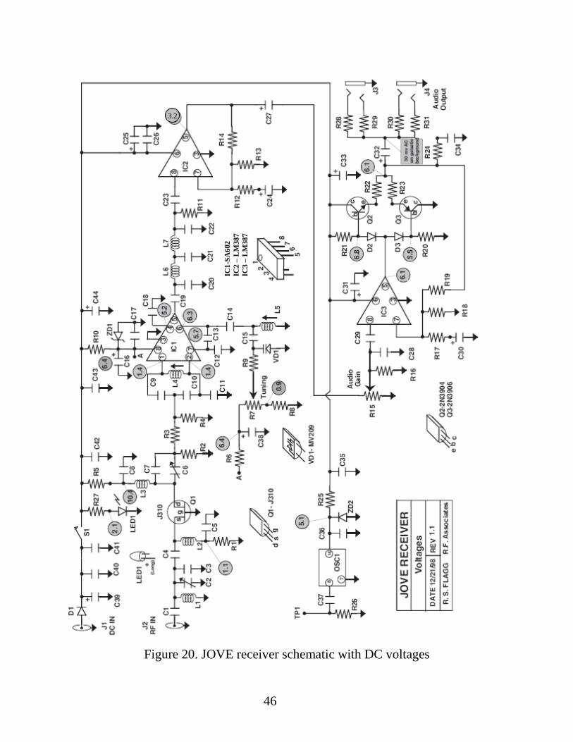
Voltage Test Points
Figure 20 and Figure 21 indicate several voltage test points on the PC board. You
should measure DC voltages at these test points and compare them to the nominal
voltages listed on the schematic. Measure the voltages using a DC voltmeter –
preferably a digital meter for better accuracy. Connect the black probe to ground
(the ground lug next to the antenna terminal is a good ground point). Check the
various test points with the red probe, being careful to touch only the test point
with the probe tip. Careless probing can result in temporary short-circuits which
can damage the receiver. You should expect a few percent difference between
your measurement and the listed values. Large discrepancies indicate a problem in
the vicinity of the circuit being tested.
Signal Injection
You can do some testing with your finger. Your body acts as an antenna for
signals radiated from the power lines (60 cycles in North America). If you touch
pin 8 of IC3 you should hear a loud buzzing sound (that is the sound of 60 cycles).
If you live near a strong AM radio station you may even hear the station. The
buzzing sound (or radio station) tells you that the signal injected from your finger
has traveled thru IC3, and the output transistors Q2 and Q3. If you hear the sound
you can conclude that this section of the circuit is probably OK. If you hear
nothing, then there is likely a problem between the input of IC3 and the audio
output.
Assuming that IC3 and Q2 /Q3 are working properly you can go back to the
previous stage of the audio amplifier circuit and test to see that a signal is getting
from the input of IC2 to the audio output. Turn up the volume control and touch
pin 8 of IC2. If the circuits between the input of IC2 and the audio output are
working you should hear the 60 cycle buzz or (or a local radio station).
I hear a broadcast station all over the dial.
Depending on your geographic location you may hear a loud station that is
everywhere on the dial. Fortunately this problem does not happen very often. It is
caused by a strong short-wave station overloading the receiver. This interference is
sometimes heard in daylight hours during times of maximum sunspot activity, but
has seldom been a problem during Jupiter observations at night. You may
experience this type of overload for a few minutes or a few hours when
propagation conditions are just right. If the problem persists during daylight
attempts to monitor the Sun you may contact the receiver designer at
[email protected] for information on a filter that has proven successful in
eliminating this interference source.

45
HELP! – if it still doesn’t work
If you need to ask one of the Jove team for assistance it is much easier for us to
help if you have documented exactly what the problem is, what measurements you
have made, and their results. A report of “my radio doesn’t work – what do you
think is wrong” is pretty useless. On the other hand a report like “I tried to align
the receiver using the test procedure but tuning C6 didn’t effect the output signal
level. All voltages were normal” can be very helpful.
If you have been unsuccessful in getting your receiver working by this point please
feel free to contact either Richard Flagg or Wes Greenman for assistance. Our
email addresses are on the Jove website at
http://radiojove.gsfc.nasa.gov/contacts.htm.
As a last resort you can make an arrangement with either Flagg or Greenman to
trouble shoot and repair your receiver for a flat fee of $25 plus shipping (flat fee
assumes that you have followed instructions with reasonable accuracy and have not
butchered the receiver).
Figure 19. Views of completed JOVE RJ1.1 receiver
46
Figure 20. JOVE receiver schematic with DC voltages
3.2
IC1
-SA
602
IC2
– L
M38
7
IC3
– L
M38
7

47
Figure 21. JOVE receiver board with DC voltages for testing
5.4

48
Appendix A
Soldering Techniques
1. Wipe the hot iron tip on a wet sponge and
tin the tip (melt a small amount of solder on
the tip). This step is not necessary prior to
every solder joint but should be done
whenever there is a build-up of residue on
the tip.
2. Touch the tip of the iron firmly to the
junction of the circuit trace and the
component lead, heating both for between 1
and 2 seconds. The iron tip should remain in
contact with the joint through step 4.
3. Apply solder to the pre-heated joint. As
the solder melts, feed a small amount
(approximately 1/4") into the pool of molten
solder forming at the junction of the solder
trace and lead. This should take no more
than 1 second.
4. Remove the solder and continue to heat
the joint for another second or until the
solder is melted, keep to a minimum the time
the joint is heated, while making sure the
solder is melted. The finished solder joint
should be shiny and flow in contact with the
component lead.
5. Cut the component lead flush with the top
of the solder joint. Be sure the cut-off wire
does not fall on the board shorting out other
connections.
Use a 15-25 watt soldering iron and
60/40 rosin core solder, 0.032" diam.

49
Appendix B
Resistor Color Code Guide
We use both the 4 and 5-band varieties of resistors.
An Example
Using
the
resisto
r
above
as an
example:
A = yellow = 4, B = violet = 7, C = Orange = 103 = 1000, D = gold = 5%
The resistor value is 47,000 Ohms and it has a 5% tolerance.
The multiplier 1000 is also known as kilo (k), so the resistor is 47 kOhms.
If the multiplier were blue = 106 = 1,000,000 [mega (M)], then the resistor value
would be 47 MOhms - pronounced 47 mega-Ohms.
APPENDIX C
ABC D
A. First significant figure of resistance in ohms
B. Second significant figure of resistance in ohms
C. Decimal multiplier
D. Resistance tolerance in percent (gold = 5%, silver = 10%)

50
Jove 1.1 Receiver Specifications
Since this receiver is normally built as a kit it is not possible to guarantee
specifications – which depend upon how well the tune-up was performed.
However, the following specifications are typical.
GAIN – The gain depends upon the setting of the audio gain control. With max
clockwise gain (volume) setting the receiver gain is > 100 dB.
BANDWIDTH – the audio low pass filter response is down 3 dB at 3.5 kHz.
Since the receiver is a direct conversion type the equivalent RF bandwidth is 7
kHz.
NOISE FIGURE – 6dB or better
TUNING – Tuning information is presented for 3 receivers below. These
receivers use the new Jove receiver front panel (summer 2010). Tuning knob
position refers to the radial tick marks printed around the tuning knob – where
position 1 is the full CCW position mark. Position numbers increase as the knob is
rotated clockwise.


![IgY JoVE Protocol 3084[1]](https://static.fdocuments.us/doc/165x107/577d242a1a28ab4e1e9bc162/igy-jove-protocol-30841.jpg)


