Rise and fall time regulation with current source MOSFET ...
33
Application Note Please read the Important Notice and Warnings at the end of this document V 1.0 www.infineon.com page 1 of 33 2020-06-19 Z8F69449874 Rise and fall time regulation with current source MOSFET gate drivers About this document Scope and purpose This application note proposes an algorithm to control MOSFET’s rise and fall times with current source MOSFET gate driver ICs in PWM operation. It explains the settings of the MOSFET driver which affect the rise and fall times and it analyzes the behavior of the proposed algorithm under different scenarios with the help of some measurements with the Motor System IC TLE9562. The described closed loop control of the MOSFET’s rise and fall times has been designed to compensate the parameter variation of the MOSFET types, the spread of the MOSFETs and of the gate driver. It is suitable for embedded systems since it minimizes the required memory and processing resources by using fixed-point arithmetic and an adaptive decision tree which bases on the EMA (Exponential Moving Average) of the measured rise times. Intended audience This document is intended for users who develop the embedded software to control the MOSFET’s rise and fall times with devices integrating current source MOSFET gate drivers with on-chip switching time measurement such as the Motor System ICs (TLE956x), the Multi MOSFET driver ICs (TLE9210x), and Embedded Power ICs (TLE985x). Table of contents About this document ....................................................................................................................... 1 Table of contents ............................................................................................................................ 1 1 Glossary ................................................................................................................................ 3 2 Introduction .......................................................................................................................... 6 3 Considered circuit .................................................................................................................. 8 4 Influence of configuration parameters in TRISEx ....................................................................... 9 4.1 Phases when switching on ...................................................................................................................... 9 4.2 Measurements with static pre-charge and charge currents ................................................................ 11 4.3 Measurements with a changing pre-charge current ............................................................................ 12 4.4 Measurements with a changing charge current ................................................................................... 13 4.4.1 Switching behavior .......................................................................................................................... 13 4.4.2 Conducted electromagnetic emissions........................................................................................... 14 5 EMA-based hysteresis algorithm to regulate tRISEx .................................................................. 16 5.1 Requirements on the algorithm............................................................................................................ 16 5.2 Implementation..................................................................................................................................... 17 5.2.1 Initialization phase ........................................................................................................................... 18 5.2.2 EMA calculation phase ..................................................................................................................... 18 5.2.3 Adaptive hysteresis decision tree phase ......................................................................................... 19 5.3 Measurements ....................................................................................................................................... 20 5.3.1 Varying INITIAL_ICHGx ..................................................................................................................... 20
Transcript of Rise and fall time regulation with current source MOSFET ...

Application Note Please read the Important Notice and Warnings at the end of this document V 1.0
www.infineon.com page 1 of 33 2020-06-19
Z8F69449874
Rise and fall time regulation with current
source MOSFET gate drivers
About this document
Scope and purpose
This application note proposes an algorithm to control MOSFET’s rise and fall times with current source
MOSFET gate driver ICs in PWM operation. It explains the settings of the MOSFET driver which affect the rise and
fall times and it analyzes the behavior of the proposed algorithm under different scenarios with the help of
some measurements with the Motor System IC TLE9562.
The described closed loop control of the MOSFET’s rise and fall times has been designed to compensate the parameter variation of the MOSFET types, the spread of the MOSFETs and of the gate driver. It is suitable for
embedded systems since it minimizes the required memory and processing resources by using fixed-point
arithmetic and an adaptive decision tree which bases on the EMA (Exponential Moving Average) of the
measured rise times.
Intended audience
This document is intended for users who develop the embedded software to control the MOSFET’s rise and fall times with devices integrating current source MOSFET gate drivers with on-chip switching time measurement
such as the Motor System ICs (TLE956x), the Multi MOSFET driver ICs (TLE9210x), and Embedded Power ICs
(TLE985x).
Table of contents
About this document ....................................................................................................................... 1
Table of contents ............................................................................................................................ 1
1 Glossary ................................................................................................................................ 3
2 Introduction .......................................................................................................................... 6
3 Considered circuit .................................................................................................................. 8
4 Influence of configuration parameters in TRISEx ....................................................................... 9
4.1 Phases when switching on ...................................................................................................................... 9
4.2 Measurements with static pre-charge and charge currents ................................................................ 11 4.3 Measurements with a changing pre-charge current ............................................................................ 12 4.4 Measurements with a changing charge current ................................................................................... 13
4.4.1 Switching behavior .......................................................................................................................... 13
4.4.2 Conducted electromagnetic emissions ........................................................................................... 14
5 EMA-based hysteresis algorithm to regulate tRISEx .................................................................. 16
5.1 Requirements on the algorithm............................................................................................................ 16 5.2 Implementation..................................................................................................................................... 17
5.2.1 Initialization phase ........................................................................................................................... 18 5.2.2 EMA calculation phase ..................................................................................................................... 18 5.2.3 Adaptive hysteresis decision tree phase ......................................................................................... 19 5.3 Measurements ....................................................................................................................................... 20 5.3.1 Varying INITIAL_ICHGx ..................................................................................................................... 20

Application Note 2 of 33 V 1.0
2020-06-19
Rise and fall time regulation with current source MOSFET gate
drivers Glossary
5.3.2 Varying tRISEx_TG ............................................................................................................................ 24
6 Conclusions and future work .................................................................................................. 26
7 Appendix A: Calculating INIT_ICHGx to boost the algorithm’s convergence ................................. 27
8 Appendix B: Source code EMA-based hysteresis algorithm ......................................................... 29
9 References ........................................................................................................................... 31
Revision history............................................................................................................................. 32

Application Note 3 of 33 V 1.0
2020-06-19
Rise and fall time regulation with current source MOSFET gate
drivers Glossary
1 Glossary
This section explains the meaning of the terms used in this application note
Table 1 Glossary of terms
Term Definition
Active MOSFET MOSFET that is switched on with the rising edge of the PWM signal. In the tests
presented in this document, the Active MOSFET is always the high-side MOSFET
Adaptive Gate
Control
MOSFET driver’s control scheme in which the pre-charge current is automatically
adjusted to regulate the turn-on and turn-off delay
αx Algorithm’s alpha constant that weights the samples for the EMA calculation
Crss MOSFET’s reverse transfer capacitance, which corresponds to the gate-drain
capacitance
di/dt Switching phase at the MOSFET characterized by a large variation of the drain-source
current when the gate-source voltage is between the threshold and the Miller plateau
voltage
dv/dt Switching phase at the MOSFET characterized by a large variation of the drain-source
voltage while the gate-source voltage is at the Miller plateau voltage
ECU Electronic control unit
EMA Algorithm’s exponential moving average
EOS Algorithm’s end of scale constant of the used variable type
fc1_x First cut off frequency of the amplitude of the harmonics of the VSHx’s trapezoidal
waveform approximation. fc1_x is determined by the frequency of the waveform
fc2_x Second cut off frequency of the amplitude of the harmonics of the VSHx’s trapezoidal
waveform approximation. fc2_x is determined by the frequency of the waveform
FPA Fixed-Point Arithmetic
fSWx Frequency of the trapezoidal waveform to which VSHx is approximated
Generator Mode
Detection
MOSFET driver’s control scheme that automatically detects in which direction the drain current is flowing. Basing on this information, it applies the Active MOSFET gate
current patterns either to the high-side or the low-side MOSFET
HBx Half-bridge x
HSx High-side MOSFET at HBx. MOSFET in the half-bridge whose drain is connected to Vs
ICHGFWx MOSFET driver’s current sunk to turn off the freewheeling MOSFET of half-bridge x,
configured by SPI
ICHGx MOSFET driver’s current sourced to the Active MOSFET of the half-bridge x during the
charge phase, configured by SPI
ICHGMAXx MOSFET driver’s max. pre-charge current. IPRECHGx is limited to ICHGMAXx,
configured by SPI
Id Drain-source current flowing through MOSFET
IDS_HSx Drain-source current flowing through the high-side MOSFET of HBx
IG_activex MOSFET driver’s current to the gate of the Active MOSFET of half-bridge x. It is positive
when the current flows into the MOSFET’s gate. In the tests presented in this
document, the Active MOSFET is always the high-side MOSFET

Application Note 4 of 33 V 1.0
2020-06-19
Rise and fall time regulation with current source MOSFET gate
drivers Glossary
IG_HSx MOSFET driver’s current to the gate of high-side MOSFET of half-bridge x. It is positive
when the current flows into the MOSFET’s gate
IG_LSx MOSFET driver’s current to the gate of low-side MOSFET of half-bridge x. It is positive
when the current flows into the MOSFET’s gate
IHOLD MOSFET driver’s hold current sourced or sunk to keep the MOSFET in the desired state,
configured by SPI
IIR Infinite Impulse Response filter
INIT_ICHGx Algorithm’s initialization value constant of ICHGx
IPCHGINITx MOSFET driver’s pre-charge current sourced by the gate driver to the Active MOSFET of
the half-bridge x during tPCHGx, configured by SPI
LSx Low-side MOSFET at HBx. MOSFET in the half-bridge whose source is connected to
ground
MAX_ICHGx Algorithm’s maximum value constant to which the ICHGx will be regulated
MIN_ICHGx Algorithm’s minimum value constant to which the ICHGx will be regulated
m_ichgx Algorithm’s variable that stores the current ICHGx
m_trisex_ema[] Algorithm’s array in which the calculated EMAs for the different configured ICHGx are
stored
PWMz External PWM (Pulse Width Modulation) signal applied to the input pin PWMz
Qgd MOSFET’s gate-drain charge, measured with Vdd = 32V
Qg _mi_app_activex Active MOSFET’s gate charge while the MOSFET is at the Miller plateau, measured with a Vdd equal to the Vs of the application. In the tests presented in this document, the
Active MOSFET is always the high-side MOSFET
Qg_mi_app_hsx High-side x’s gate charge, measured with a Vdd equal to the Vs of the application
SBC System basis chip
tDONx MOSFET driver’s measurement of turn-on delay of the Active MOSFET of half-bridge x
tDOFFx MOSFET driver’s measurement of turn-off delay of the Active MOSFET of half-bridge x
tFALLx MOSFET driver’s measurement of the fall time when the Active MOSFET switches off,
measured at VSHx from VSHH to VSHL
tFALLx_100 Fall time of VSHx measured from Vs to 0
tFVDS MOSFET driver’s drain source overvoltage filter time
tHBxBLANK Active MOSFET driver’s active drain source overvoltage blank time of half bridge-x, configured
by SPI
tHBxCCP_FW MOSFET driver’s freewheeling cross current protection time of half bridge-x,
configured by SPI
Tj Junction temperature of the MOSFET
tOFFx Time during which VSHx is low, 0V
tONx Time during which VSHx is high, Vs
tPCHGx MOSFET driver’s duration of the pre-charge phase of half-bridge x, configured by SPI
tRISEx MOSFET driver’s measurement of the rise time when the MOSFET switches on, measured at VSHx from VSHL to VSHH. For the TLE956x, the value of tRISEx in ns is
obtained by multiplying the value of tRISEx in the register by 53.3 ns.
tRISEx_100 Rise time of VSHx measured from 0 to Vs
Application Note 5 of 33 V 1.0
2020-06-19
Rise and fall time regulation with current source MOSFET gate
drivers Glossary
tRISEx_L Linearized rising edge of VSHx
tRISEx_TG Algorithm’s target rise time constant of VSHx from VSHL to VSHH
tSWx Period of the trapezoidal waveform to which VSHx is approximated
uC Microcontroller
Vdd MOSFET’s drain source voltage
Vds MOSFET’s drain-source voltage
Vgd MOSFET’s gate-drain voltage
Vgs MOSFET’s gate-source voltage
VGS_HSx Gate-source voltage of the high-side at the half-bridge x
VGSMI_activex Miller plateau gate-source voltage of the Active MOSFET at the half-bridge x. In the
tests presented in this document, the Active MOSFET is always the high-side MOSFET
VGSMI_HSx Miller plateau gate-source voltage of the high-side at the half-bridge x
VGSTH_HSx Threshold gate-source voltage of the high-side at the half-bridge x
Vs Supply voltage of the IC and DC link voltage of the half-bridges, protected against
reverse polarity
VSHx Voltage at the phase of half-bridge x
VSHH MOSFET driver’s high threshold at SHx, typically Vs - 2.25 V
VSHL MOSFET driver’s low threshold at SHx, typically 2.25 V
x Related to half-bridge x
z Related to the PWM input signal z

Application Note 6 of 33 V 1.0
2020-06-19
Rise and fall time regulation with current source MOSFET gate
drivers Introduction
2 Introduction
The Infineon’s Motor System ICs (TLE956x) and Multi MOSFET driver ICs (TLE9210x) include a MOSFET driver with multi-stage current source gate control which is configured over SPI. Over this interface, a set of gate currents, that are sequentially sourced to or sunk from the gate of the MOSFET during certain time intervals,
can be configured in order to control following switching times:
Turn-on (tDONx) and turn-off (tDOFFx) delays: the Adaptive functionality of the MOSFET driver automatically regulates the pre-charge and pre-discharge currents to achieve the target tDONx and tDOFFx configured by the user. The application note [1] and the data sheets of the mentioned devices contain
detailed information on how to configure this functionality.
Rise (tRISEx) and fall (tFALLx) times: the MOSFET driver enables the user to implement a software algorithm to regulate the (dis)charge current I(D)CHGx and achieve the target rise (tRISEx_TG) and fall (tFALLx_TG)
times by providing the currently measured tRISEx and tFALLx in its status registers.
Controlling the tRISEx and tFALLx in PWM operation is of big interest for the user, since these timings have a
direct influence on the power losses and on the electromagnetic emissions. As a matter of fact, it has been demonstrated in [2] that too short tRISEx and tFALLx lead to high electromagnetic emissions, while too large
tRISEx and tFALLx increase the power losses. In order to achieve an accurate tRISEx and tFALLx, it is not sufficient to configure I(D)CHGx in open loop due to
following reasons:
The MOSFET’s Qgd has a deviation between the typical and maximum value, as shown in Figure 1.
The I(D)CHGx sourced by the gate driver has some tolerances.
The MOSFETs Miller plateau depends on operating conditions such as junction temperature Tj, load current
Id and drain voltage Vdd as depicted in Figure 1, which can change during runtime.
Aging leads to changes in the V-I characteristics of the MOSFETs as analyzed in [3].
Figure 1 Qgd deviations, transfer characteristics and typical gate charge of the IPZ40N04S5-3R1

Application Note 7 of 33 V 1.0
2020-06-19
Rise and fall time regulation with current source MOSFET gate
drivers Introduction
In order to face these challenges, this application note proposes an algorithm that reconfigures the charge current ICHGx in closed loop to achieve the targeted rise (tRISEx_TG) time, which is based on the tRISEx
measurements provided by the gate driver. This document is structured as follows: first, the configuration parameters of the MOSFET driver that influence
the tRISEx and tFALLx are presented, supported with measurements. Next, the requirements on the algorithm are derived from the previous measurements and from the application assumptions, followed by a detailed
explanation of the algorithm and by a set of measurements performed with it. Then, conclusions are drawn and the future work is discussed. Two appendixes conclude this application note with the calculations needed to
boost the convergence of the algorithm and with the source code of the algorithm.

Application Note 8 of 33 V 1.0
2020-06-19
Rise and fall time regulation with current source MOSFET gate
drivers Considered circuit
3 Considered circuit
The circuit considered and tested in this application note, unless explicitely indicated otherwise, is as depicted in Figure 2.
Vbat
GH3
Reverse polarity
protection
HS3
LS3
DC
Motor
MGL3
SL
SH3
Vs
PWM3
SPI
Vcc
Multi-MOSFET
Driver IC
SBC / Vreg
Gnd
Gnd
Vcc
Gnd
PWM SPI1
uC
Gnd
VsVbat
CP
VCP
=
Power
Supply
+
4
Vs
Active
PWM
MOSFET
Free-
wheeling
MOSFET
SPI2
Logging
ECU
Figure 2 Simplified circuit used for the tests
Following components make up the circuit:
MOSFET driver IC: Motor System IC TLE9562 (on Evaluation Board TLE9562). The Adaptive Gate Control and
the Generator Mode Detection are off throughout all the tests in this document. For this document, the external signal PWM3 was assigned to HB3 (bit PWM3MAP = 0 in register GENCTRL).
SBC / Vreg: Motor System IC TLE9562 (on Evaluation Board TLE9562).
MOSFETs: IPZ40N04S5-3R1 (on Evaluation Board TLE9562).
uC: Aurix 2G TC275 (on Triboard). The microcontroller generates a PWM signal of 20 kHz and 50% duty cycle
which is connected to the PWM3 input of the TLE9562. The microcontroller also configures the MOSFET
driver over SPI1, runs the algorithm explained in Chapter 5 and reads TRISE3 over SPI1 from the MOSFET driver. In addition, it sends TRISE3, together with some variables of the algorithm, over SPI2 for logging purposes. This logging is analyzed with an oscilloscope.
DC Motor: 36W DC Motor Ref 321-3186, without starting capacitors and without load.
All the tests presented in this document have been executed with a Vbat of 13 V and at room temperature.

Application Note 9 of 33 V 1.0
2020-06-19
Rise and fall time regulation with current source MOSFET gate
drivers Influence of configuration parameters in TRISEx
4 Influence of configuration parameters in TRISEx
This chapter first explains the phases and parameters that can be configured in the MOSFET driver to shape the switching-on of a MOSFET. In the following subsections of this chapter, the measurements conducted with different values of the configurations parameters that influence tRISEx are shown. Finally, the influence of
different tRISEx on conducted electromagnetic emissions is discussed on basis of measurements with a spectrum analyzer.
4.1 Phases when switching on
The MOSFET driver is a gate driver with current timing control and current level control, which splits the switching-on of the Active MOSFET into four phases. This allows shaping the in-transition slope as shown in [4],
which allows reducing the power losses [2] and the electromagnetic emissions [5] with respect to voltage gate
drivers or gate drivers with constant current. In each phase, the configured amount of current is sourced or sunk to / from the gate as shown in Figure 3.
Each phase starts right away when the previous phase ends:
1) Cross-current protection: starts at the rising edge of the synchronized PWMz signal that was assigned to
HBx, and ends when tHBxCCP_FW elapses. In this phase, LSx is switched off and HSx is kept off with -IHOLD. 2) Pre-charge: it lasts for the tPCHGx configured in the corresponding register. It is recommended to configure
tPCHGx in such a way that the pre-charge phase ends when VGSTH_HSx is reached, i.e. before the di/dt
transition starts at the MOSFET. Otherwise, a very large di/dt transition would cause a large voltage
difference at the parasitics of the commutation path, leading to voltage overshoots that would increase the electromagnetic conducted emissions, as demonstrated in [5]. During the pre-charge phase, the current
level IPCHGINITx configured in the register is sourced to the gate of HSx (note that it is considered that the
Adaptive functionality is off).
3) Charge: it starts right after the pre-charge phase and it ends when VSHx reaches VSHH, which is
automatically detected by a fast comparator inside the MOSFET driver. At the charge phase, the current level ICHGx configured in the corresponding register is sourced to the gate of HSx. During this phase, the
di/dt transition (VGS_HSx raises from VGSTH_HSx to VGSMI_HSx) and dv/dt transition (VGS_HSx is at the Miller plateau: VGSMI_HSx) should take place at the MOSFET. tRISEx can be controlled with ICHGx, which will actually be the goal of the algorithm proposed in Chapter 5.
4) Post-charge: it starts when VSHx reaches VSHH and it ends when tFVDS elapses. During this phase, the
current sourced to the gate of HSx is successively increased until ICHGMAXx is reached (this can be disabled in a control register). Afterwards, HSx is kept on with IHOLD.

Application Note 10 of 33 V 1.0
2020-06-19
Rise and fall time regulation with current source MOSFET gate
drivers Influence of configuration parameters in TRISEx
CR
OS
S
CU
RR
EN
T
PR
OT
EC
TIO
N
PR
E-C
HA
RG
E
CH
AR
GE
PO
ST
-
CH
AR
GE
VSHx
VSHL
VSHH
IG_HSx
IGS_LSx
ICHGMAXx
ICHGx
VGS_HSx
tDONx
tRISEx
VSHL
0
Synchronized
intern. PWMz
t
t
t
t
tPCHGx
t
IDS_HSx
tHBxCCP FW tHBxBLANK Active
VSHH
VS
IHOLD
tFVDS
External
PWMz
t
t
HS
x
Mo
tor
as
loa
d
LS
x
- ICHGFWx
IPCHGINITx
-IHOLD
VGSTH_HSx
VGSMI_HSx
Figure 3 Switching on phases for the Active MOSFET

Application Note 11 of 33 V 1.0
2020-06-19
Rise and fall time regulation with current source MOSFET gate
drivers Influence of configuration parameters in TRISEx
4.2 Measurements with static pre-charge and charge currents
In this subsection, the MOSFET driver is configured with a certain tPCHGx, IPCHGINITx and ICHGx to analyze the
stability of IG_HSx and consequently, the stability of the rise time of VSHx measured with the scope and the tRISEx measured by the MOSFET driver.
The values of tPCHG3 and IPCHGINIT3 are selected in such a way that the pre-charge phase ends when VGSTH_HS3 is reached, typically 2.8V for the selected MOSFET. ICHG3 is selected so that a mean tRISE3 of 586
ns is achieved. In Table 2, the configured values are shown.
Table 2 MOSFET driver configuration
Parameter Value in register Value according to datasheet
tPCHG3 2 214 ns
IPCHGINIT3 25 20.8 mA
ICHG3 9 3.7 mA
The oscilloscope is in persistence mode to superimpose 5000 samples. In Figure 4, it can be observed that IG_HS3 is very stable, which leads to a very small standard deviation of 4.7 ns in the rise time measurements of VSH3.
Figure 4 Persistence of IG_HS3, VSH3 and VGS_HS3
In the meantime, the tRISE3 values measured by the MOSFET driver have been read through SPI and decoded with the oscilloscope as shown in Figure 5. It can be observed that tRISE3 has a mean value of 11.5 (612 ns), which is very close to the rise time measured by the oscilloscope (546 ns, shown in Figure 4).
Due to the resolution of the tRISE3 measurement of the MOSFET driver, which is 53.3 ns in the TLE956x and corresponds to its clock cycle, tRISE3 changes between two values: 11 and 12, which correspond to 586 ns (11 · 53.3 ns) and 639 ns (12 · 53.3 ns) respectively.
IG_HS3
VGS_HS3
VSH3

Application Note 12 of 33 V 1.0
2020-06-19
Rise and fall time regulation with current source MOSFET gate
drivers Influence of configuration parameters in TRISEx
Please note that throughout this application note there will be some small mismatches between the tRISEx measured by the MOSFET driver and the rise time measured by the scope. This is because VSHH and VSHL of
the MOSFET driver do not exactly match the thresholds of the oscilloscope.
Notice that in all the snapshots in these documents, the tRISEx value measured by the MOSFET driver will be slightly different to the value measured with the scope. This is mainly because the VSHL and VSHH thresholds
do not exactly match with the thresholds with which the oscilloscope measures the rise time.
Figure 5 TRISE3 measurements of MOSFET driver
4.3 Measurements with a changing pre-charge current
In this subsection, tPCHGx and ICHGx are not changed and IPCHGINITx is set to three different values to show
that IPCHGINIT does not have any influence on the rise time if these three parameters are configured properly. Both tPCHG3 and IPCHGINIT3 are configured in a way that the rise time is only controlled by ICHG3, i.e. the pre-
charge phase ends before the di/dt and dv/dt phases start. In Table 3, the configured values are shown.
Table 3 MOSFET driver configuration
Parameter Value in register Value according to datasheet
tPCHG3 2 214 ns
IPCHGINIT3 25, 26, 27 20.8, 22.4, 24.1 mA
ICHG3 9 3.7 mA
While IPCHGINIT3 is being changed between the three values, the oscilloscope is in persistence mode to
superimpose the three samples. In Figure 6, it can be observed that changing IPCHGINIT3 does not have an impact on the rise time (VSH3 rising edges are parallel) but only on the delay-on time. This is a good indicator that both tPCHG3 and IPCHGINIT3 are properly configured in a way that the pre-charge phase ends before the
di/dt of the MOSFET starts, i.e. when VGSTH_HS3 is reached.
tRISE3 = 12
tRISE3 = 11

Application Note 13 of 33 V 1.0
2020-06-19
Rise and fall time regulation with current source MOSFET gate
drivers Influence of configuration parameters in TRISEx
Figure 6 Persistence of IG_HS3, VSH3 and VGS_HS3 while IPCHGINIT3 is increased
4.4 Measurements with a changing charge current
In this subsection, it is investigated how different values of ICHGx affect the switching-on behavior and the electromagnetic emissions.
4.4.1 Switching behavior
The MOSFET driver is configured with a fixed tPCHGx and IPCHGINITx. ICHGx is changed between three values to analyze how they influence the delay-on time and the rise time. In Table 4, the configured values are shown.
Table 4 MOSFET driver configuration
Parameter Value in register Value according to datasheet
tPCHG3 2 214 ns
IPCHGINIT3 25 20.8 mA
ICHG3 9, 10, 11 3.7, 4.3, 5.0 mA
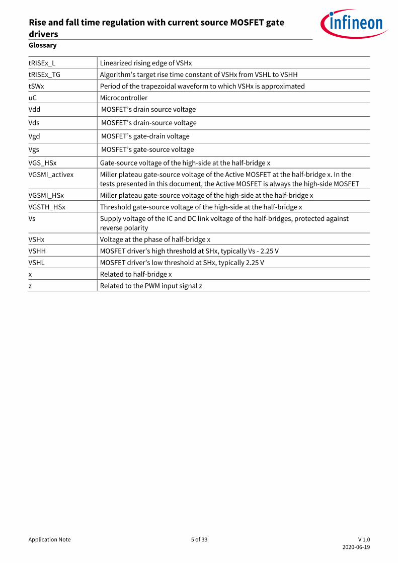
While ICHG3 is being changed between the three values, the oscilloscope is in persistence mode to superimpose the three samples. In Figure 7, it can be observed that changing ICHG3 has an impact on both the
delay-on time and on the rise time (VSH3 rising edges are not parallel). Note that during the charge phase, we are controlling both the di/dt transition (VGS_HS3 from VGSTH_HS3 to VGSMI_HS3) and the dv/dt transition (VGS_HS3 at the Miller plateau, VGSMI_HS3) of the MOSFET. In addition, it can be observed that an increase of ICHG3 by just one value causes a large change in the rise time of around 200 ns. Since the values
that can be configured for ICHG3 are discrete, the achievable TRISE3 will be discrete too.
IG_HS3
VGS_HS3
VSH3
Application Note 14 of 33 V 1.0
2020-06-19
Rise and fall time regulation with current source MOSFET gate
drivers Influence of configuration parameters in TRISEx
Figure 7 Persistence of IG_HS3, VSH3 and VGS_HS3 while ICHG3 is increased
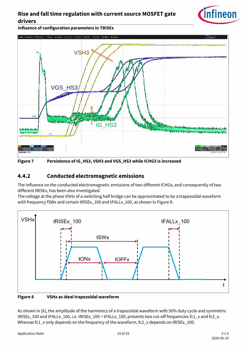
4.4.2 Conducted electromagnetic emissions
The influence on the conducted electromagnetic emissions of two different ICHGx, and consequently of two different tRISEx, has been also investigated. The voltage at the phase VSHx of a switching half bridge can be approximated to be a trapezoidal waveform
with frequency fSWx and certain tRISEx_100 and tFALLx_100, as shown in Figure 8.
Figure 8 VSHx as ideal trapezoidal waveform
As shown in [6], the amplitude of the harmonics of a trapezoidal waveform with 50% duty cycle and symmetric
tRISEx_100 and tFALLx_100, i.e. tRISEx_100 = tFALLx_100, presents two cut-off frequencies fc1_x and fc2_x. Whereas fc1_x only depends on the frequency of the waveform, fc2_x depends on tRISEx_100.
IG_HS3
VGS_HS3
VSH3

Application Note 15 of 33 V 1.0
2020-06-19
Rise and fall time regulation with current source MOSFET gate
drivers Influence of configuration parameters in TRISEx
𝑓𝑐1_𝑥 = 2
𝜋 ∙ 𝑡𝑆𝑊𝑥
𝑓𝑐2_𝑥 = 1
𝜋 ∙ 𝑡𝑅𝐼𝑆𝐸𝑥_100
In Figure 9, the dashed lines illustrate the boundaries of the harmonics’ amplitude of two ideal trapezoidal
waveforms corresponding to two VSHx with the same fSWx and different tRISEx_100. It can be observed that the boundaries decrease with a ratio of:
-20 dB / decade: for frequencies between fc1_x and fc2_x
-40 dB / decade: for frequencies higher than fc2_x.
Consequently, a large tRISEx leads to a lower fc2_x, which in turn causes lower electromagnetic emissions at
lower frequencies. If we extrapolate this to a switching VSHx, a lower ICHGx would lead to lower
electromagnetic emissions. This has been tested with the TLE956x for two different ICHGx switching with an
fSWx of 20 kHz, a duty cycle of 50% and with symmetrical tRISEx_100 and tFALLx_100. Table 5 shows the tested ICHGx, the tRISEx_100 measured with the oscilloscope and the calculated cut-off frequencies.
Table 5 Tested ICHGx, measured tRISEx and calculated cutoff frequencies
ICHGx tRISEx_100 measured with
scope
Calculated fc1_x Calculated fc2_x
2 mA 566 ns 12 kHz 562 kHz
10 mA 118 ns 12 kHz 2.6 MHz
The measured electromagnetic emissions shown in Figure 9 revealed that for frequencies higher than fc2_x =
2.6 MHz, the amplitude of the harmonics for a VSHx that switches with a tRISEx_100 of 566 ns is 10 dB lower
than for a VSHx that switches with 118 ns.
Figure 9 Conducted electromagnetic emissions at VSHx, switching with 20 kHz and 50% duty cycle

Application Note 16 of 33 V 1.0
2020-06-19
Rise and fall time regulation with current source MOSFET gate
drivers EMA-based hysteresis algorithm to regulate tRISEx
5 EMA-based hysteresis algorithm to regulate tRISEx
In this chapter, an algorithm that regulates ICHGx in closed loop to achieve a tRISEx_TG is proposed. This algorithm is meant to be executed by a microcontroller during run time, i.e. while the half-bridges are switching, and reconfigures ICHGx according to the tRISEx provided by the MOSFET driver, as shown in Figure
10.
Figure 10 Closed control loop of the algorithm
5.1 Requirements on the algorithm
The EMA-based (Exponential Moving Average) hysteresis algorithm has been designed to fulfill the following
requirements:
React to variations in tRISEx during operation: ICHGx is regulated every time the microcontroller
executes the algorithm. If tRISEx changes due to, for instance, variations of Vs, load, temperature or due to
MOSFETs aging, the algorithm will reconfigure the ICHGx so that the measured tRISEx matches tRISEx_TG.
Do not base on MOSFET or MOSFET driver electrical parameters: the algorithm does not need the
electrical parameters of the MOSFET or of the MOSFET driver. In this manner, the same software can be used with different MOSFETs without having to parametrize or modify the software of the microcontroller. Therefore, the often large tolerances of the electrical parameters will not affect the performance of the
algorithm.
Avoid toggling between consecutive ICHGs: it has been shown in Section 4.4.2 that the conducted
electromagnetic emissions increase with an increasing ICHGx and consequently with a decreasing tRISEx. In addition, it has been discussed in Section 4.4.1 that the tRISEx achieved with the MOSFET driver are
discrete. This implies that if the algorithm continuously toggled between two consecutive ICHGx, the electromagnetic emissions would increase, since they would be dominated by the shortest tRISEx. Therefore, if the exact tRISEx_TG cannot be achieved, the algorithm will not toggle between two consecutive ICHGx.
Suitable for execution in embedded systems: the algorithm is meant to be executed in embedded
systems with a small RAM and limited processing resources. It bases on the EMA IIR filter, which allows storing only the previously calculated average instead of having to buffer all the sampled tRISEx. The EMA is implemented in Fixed-Point Arithmetic (FPA) to avoid storing the EMA of the tRISEx as floating-point variables and consequently to avoid also complex calculations in floating-point arithmetic that would
increase the processing time.
In addition, the algorithm does not need to be executed on a strictly periodical manner, it suffices to execute it whenever the microcontroller is idle.

Application Note 17 of 33 V 1.0
2020-06-19
Rise and fall time regulation with current source MOSFET gate
drivers EMA-based hysteresis algorithm to regulate tRISEx
5.2 Implementation
In this section, the implementation of the algorithm is presented. For the sake of simplicity, the rescaling for
the FPA has not been included. For the exact implementation with FPA, please refer to the code in Section 8. The algorithm needs following constants:
αx: alpha can take a value between 0 and 1. This constant weights the samples for the EMA calculation. With an αx > 0.5, the contribution of the last measured tRISEx will be larger than the contribution of the
previously calculated EMA.
EOS: end of scale of the variable type of m_trisex_ema[]. For example, 65535 if it is declared as a 16 bits unsigned integer.
INIT_ICHGx: initialization value of ICHGx. This is the first ICHGx with which the MOSFET driver is configured.
MAX_ICHGx: maximum value for ICHGx. The algorithm will not configure the MOSFET driver with an ICHGx
higher than this value. This constant is also a safety mechanism that will prevent the MOSFET driver from switching too fast. The minimum value for this constant is MIN_ICHGx + 1, and the maximum is 63 in the case of the TLE956x.
MIN_ICHGx: minimum value for ICHGx. The algorithm will not configure the MOSFET driver with an ICHGx
lower than this value. This constant can be understood as a safety mechanism that will prevent the MOSFET driver from switching too slow. The minimum value for this constant is 0, and the maximum is MAX_ICHGx - 1.
tRISEx_TG: tRISEx target from VSHL to VSHH. The goal of the algorithm is that the tRISEx measured by the
MOSFET driver is equal to tRISEx_TG.
The algorithm also declares following variables:
m_ichgx: current ICHGx with which the MOSFET driver is configured.
m_trisex_ema[]: array of the calculated tRISEx EMAs for the different configured ICHGx. Although ICHGx can
be configured to 64 different values in the TLE956x, the number of different ICHGx that the algorithm will
configure is limited by MAX_ICHGx and MIN_ICHGx. Hence, the number of elements of the array is declared to (MAX_ICHGx - MIN_ICHGx + 1) in order to minimize the required RAM.
For example, if MAX_ICHGx = 63 and MIN_ICHGx = 0, m_trisex_ema[63] contains the tRISEx EMA calculated for ICHGx = 63, which corresponds to 100 mA in the TLE956x.
The algorithm consists of three main phases: initialization, EMA calculation and adaptive hysteresis decision tree, as shown in Figure 11.
Figure 11 Algorithm phases

Application Note 18 of 33 V 1.0
2020-06-19
Rise and fall time regulation with current source MOSFET gate
drivers EMA-based hysteresis algorithm to regulate tRISEx
5.2.1 Initialization phase
This phase is executed only once before the algorithm runs for the first time. In this phase, the ICHGx of the
MOSFET driver and the variable m_ichgx are initialized with the defined INIT_ICHGx. The user should define a value for INIT_ICHGx which is large enough to completely switch on the MOSFET before tHBxBLANK Active
expires, as shown in Figure 3. In Chapter 7, it will be discussed how the user can select INIT_ICHGx to accelerate the convergence of the algorithm, i.e. achieve tRISEx_TG faster. As depicted in Figure 12, the array
m_trisex_ema is initialized as well. The elements with an index lower than INIT_ICHGx-MIN_ICHGx are initialized with 0 and the rest of the elements with EOS. This will ensure a proper start-up of the algorithm in the adaptive decision tree, as will be shown in Section 5.2.3 and with an example in Section 5.3.1.
Figure 12 Initialization phase
5.2.2 EMA calculation phase
The EMA is an IIR filter that differently weights the last sample (with αx) and the previous samples (with 1- αx),
where αx is a constant between 0 and 1, as presented in [7].
The calculation of the EMA for tRISEx can be easily performed in an embedded system, since there it is no need
of storing all sampled tRISEx. Instead, the previous samples are indirectly pondered by weighting the EMA that was calculated the last time the algorithm ran. If m_ichgx still has the initialization value, i.e. it is the first time the algorithm configures the MOSFET driver with the current ICHGx, tRISEx is neither averaged nor weighted. In this case, tRISEx is directly stored in the
element of m_trisex_ema corresponding to the current ICHGx, as shown in Figure 13.
Figure 13 Initialization phase

Application Note 19 of 33 V 1.0
2020-06-19
Rise and fall time regulation with current source MOSFET gate
drivers EMA-based hysteresis algorithm to regulate tRISEx
In this manner, if the user sets αx to a value close to 1, the contribution of the last measured tRISEx to the EMA will be large and the algorithm will react fast to changes. On the contrary, if αx is set to a value close to 0, the
last calculated EMA will have a big influence on the currently calculated EMA, thus giving more importance to the history of the measured tRISEx than to the last tRISEx. If we draw an analogy with a conventional PI
controller, increasing αx would be equivalent to increasing the proportional and decreasing the integral gain.
This is shown in the example of Table 6, where the tRISEx EMA has been calculated for αx = 0.8 and 0.2. It can be observed that when a tRISEx of 13 is obtained at the 4th measurement, which is larger than all the
previous tRISEx, the calculated EMA is very different depending on the configured αx. For an αx = 0.8, the last measurement has a large weight and the EMA increases to 12.632. On the contrary, for an αx = 0.2, the EMA considers more importance to the history of measured tRISEx and it only increases to
11.528. Notice that the result is stored in the 9th element of the array since it is considered that all these tRISEx
are measured when an ICHGx = 9 is applied.
Table 6 Calculated EMA with αx = 0.8 and 0.2 for 4 consecutively measured tRISEx
5.2.3 Adaptive hysteresis decision tree phase
The algorithm decides in this phase whether ICHGx will be increased or decreased by 1 or if it will not change. This is done by comparing the tRISEx_TG with the tRISEx EMA calculated for the current ICHGx and for the
immediately lower and larger ICHGx, as depicted in Figure 14. Following conditions must be met to decrease ICHGx:
1. The EMA calculated for the current ICHGx is lower than tRISEx_TG. This means that the MOSFET is switching too fast, which implies that ICHGx is susceptible to be decreased.
2. The EMA that was calculated when the ICHGx was set to the immediately lower value is also lower than or equal to tRISEx_TG. This second condition makes up the hysteresis, which will prevent the algorithm
from toggling between two adjacent ICHGs. Notice that if the algorithm never configured the MOSFET driver with ICHGx – 1 before, m_trisex_ema[m_ichgx – MIN_ICHGx - 1] will still contain the initialization
value, which is 0. In this case, the condition “m_trisex_ema[m_ichgx – MIN_ICHGx - 1] ≤ tRISEx_TG” is also met.
3. The minimum ICHGx has still not been reached.
Similarly, the algorithm will increase ICHGx if these three conditions are met: 1. The EMA calculated for the current ICHGx is higher than tRISEx_TG. This means that the MOSFET is
switching too slow, which implies that ICHGx may qualify to be increased.
2. The EMA that was calculated when the ICHGx was set to the immediately higher value of the current one is also higher than or equal to tRISEx_TG. Notice that if the algorithm never configured the MOSFET driver with ICHGx + 1 before, m_trisex_ema[m_ichgx – MIN_ICHGx + 1] will still contain the initialization value, which is EOS. In this case, the condition “m_trisex_ema[m_ichgx– MIN_ICHGx + 1] ≥ tRISEx_TG” is also met.
3. The maximum ICHGx has still not been reached.
Measurement number tRISEx m_trisex_ema[9] for αx = 0.8 m_trisex_ema[9] for αx = 0.2
1 11 11 11
2 12 11.8 11.2
3 11 11.16 11.16
4 13 12.632 11.528

Application Note 20 of 33 V 1.0
2020-06-19
Rise and fall time regulation with current source MOSFET gate
drivers EMA-based hysteresis algorithm to regulate tRISEx
Figure 14 Adaptive hysteresis decision tree phase
5.3 Measurements
Several tests have been conducted to check the robustness of the algorithm in different scenarios.
The calculations have been implemented in FPA with a rescaling factor of 255. As explained in Chapter 3, the
variables of the algorithm were logged over SPI and are analyzed with an oscilloscope.
The algorithm was executed in the main loop of the microcontroller, please refer to the code of the algorithm in
Chapter 8 for the implementation.
5.3.1 Varying INITIAL_ICHGx
The algorithm has been executed with different INITIAL_ICHGx to check if tRISEx_TG can be achieved
regardless of this initial value. These are the constants which were not changed throughout the tests of this subsection:
MIN_ICHG3 = 0
MAX_ICHG3 = 63
α3 = 0.5, which implies that the last measured tRISE3 has the same weight as the historic EMA
tRISE3_TG = 11, which corresponds to 11 · 53.3 ns = 586 ns.
First, the algorithm was run with an INIT_ICHG3 = 13. In Figure 15, it can be observed at the bottom in the P1
column of the table that the algorithm achieved a mean tRISE3 = 12.64, which is not exactly tRISE3_TG = 11. As it will be shown in Figure 17, the algorithm gives more importance to avoiding the toggle of ICHG3 and tRISE3 than to minimizing the error.

Application Note 21 of 33 V 1.0
2020-06-19
Rise and fall time regulation with current source MOSFET gate
drivers EMA-based hysteresis algorithm to regulate tRISEx
Figure 15 Results with an INIT_ICHG3 = 13 and tRISE3_TG = 11
For an INIT_ICHG3 of 13, the tRISE3_ema of the adjacent ICHG3s can be observed in Figure 16. When the MOSFET driver starts switching with an ICHG3 = 13, the algorithm detects that tRISE3_TG is larger than the
calculated tRISE3_ema[13] and it decreases progressively ICHG3, which causes an increment of
tRISE3_ema[m_ichg3 - MIN_ICHG3]. tRISE3_ema[m_ichg3 + 1 - MIN_ICHG3] starts at EOS, decreases to the
calculated tRISE_ema[13] when ICHG3 is changed to 12 and then successively increases with a decreasing ICHG3. tRISE3_ema[m_ichg3 – 1 - MIN_ICHG3] stays at 0, the initialization value, which indicates that the
algorithm does not try to increase ICHG3 during this test.
Figure 16 tRISE3_ema of adjacent ICHG3s, tested with an INIT_ICHG3 = 13 and tRISE3_TG = 11
tRISE3 = 13
trise3_ema[m_ichg3-MIN_ICHG3]
VSH3
m_ichg3 = 8
trise3_ema[m_ichg3 -MIN_ICHG3] = 13
trise3_ema[m_ichg3+1-MIN_ICHG3] = 10.5
VSH3
trise3_ema[m_ichg3-1-MIN_ICHG3] = 0
tRISE3 = 12

Application Note 22 of 33 V 1.0
2020-06-19
Rise and fall time regulation with current source MOSFET gate
drivers EMA-based hysteresis algorithm to regulate tRISEx
The decisions taken by the algorithm where the cursor is pointing to on the snapshot have been depicted in blue in Figure 17. At this point, m_ichg3 = 8 and the calculated m_trise3_ema[8] is 13, which was calculated out
of all tRISE3 measured when the MOSFET driver was switching with ICHG3 = 8. Since this value is larger than tRISE3_TG=10 (11), the algorithm further checks if increasing ICHG3 would lead to a tRISE3 which would still be
larger than the target.
However, instead of directly increasing the ICHG3 to 9, the algorithm checks if an ICHG3 = 9 has been previously used and analyzes the EMA of the tRISE3 that was obtained for that ICHG3. Indeed, the tRISE3_ema[9] had been calculated previously and was 10.5. Consequently, the algorithm decides not to increase the current to prevent ICHG3 and tRISE3 from toggling. Note that this tRISE3 EMA was available in memory because the algorithm had previously configured an ICHG3 = 9 when it was decreasing ICHG3 from the INIT_ICHG3 = 13.
Figure 17 Decisions taken by the algorithm (in blue) at the cursor of Figure 16
In Figure 18, it is shown that if the INIT_ICH3 is much larger than the ICHG3 that would be necessary to achieve tRISE3_TG, the algorithm also regulates ICHG3 correctly, although the time it needs to converge is larger.

Application Note 23 of 33 V 1.0
2020-06-19
Rise and fall time regulation with current source MOSFET gate
drivers EMA-based hysteresis algorithm to regulate tRISEx
Figure 18 Results with an INIT_ICHG3 = 40 and tRISE3_TG = 11
The closer INIT_ICHGx is to the ICHGx required to achieve tRISEx_TG, the faster the algorithm converges, as
shown in Figure 19 for an INIT_ICHG3 = 11. In Chapter 7, it is explained how INIT_ICHGx can be calculated to
accelerate the convergence of the algorithm.
Figure 19 Results with an INIT_ICHG3 = 11 and tRISE3_TG = 11
tRISE3 = 13
trise3_ema[m_ichg3-MIN_ICHG3] = 12.04
VSH3
m_ichg3 = 8
tRISE3 = 13
m_ichg3 = 8
tRISE3 = 12
VSH3
tRISE3 = 12
m_ichg3 = 40
m_ichg3 = 11

Application Note 24 of 33 V 1.0
2020-06-19
Rise and fall time regulation with current source MOSFET gate
drivers EMA-based hysteresis algorithm to regulate tRISEx
The behavior of the algorithm has been also checked if ICHGx needs to be increased. Figure 20 shows that in steady state, ICHG3 is 9 and the mean tRISE3 is 10. In this test, the algorithm increases m_ichg3 from
INIT_ICHG3 = 6 until the tRISE3 EMA is lower than tRISE3_TG and it does not reduce it again to avoid toggling. This also means that neither an ICHG3 = 8 (which yields a tRISE3 mean of 12.6, see Figure 19) nor an ICHG3 = 9
(which yields a tRISE3 mean of 10, see Figure 20) would exactly achieve the configured tRISE3_TG = 11. As discussed in Chapter 4.4.1, discrete ICHGs can only achieve discrete rise times.
Figure 20 Results with an INIT_ICHG3 = 6 and tRISE3_TG = 11
5.3.2 Varying tRISEx_TG
The tests presented in the previous chapter were conducted with a tRISE3_TG = 11. This chapter shows two additional tests with different tRISEx_TG to demonstrate that the algorithm can achieve both slower and faster tRISEx.
The constants which were not changed throughout the tests of this subsection are as follows:
MIN_ICHG3 = 0
MAX_ICHG3 = 63
α3 = 0.5, which implies that the last measured tRISE3 has the same weight as the historic EMA
INIT_ICHG3 = 9
First, tRISE3_TG was set to 20, which corresponds to 1066 ns. It can be seen in Figure 21 that the algorithm first decreases ICHG3 to 5 and in steady state it selects an ICHG3 of 6 to achieve a tRISE3 closer to 20. The mean
tRISE3 is 19.9 during the 10 seconds shown in the snapshot, see P1 in the table of the figure.
tRISE3 = 11 trise3_ema[m_ichg3-MIN_ICHG3]
VSH3
m_ichg3 = 9
tRISE3 = 10

Application Note 25 of 33 V 1.0
2020-06-19
Rise and fall time regulation with current source MOSFET gate
drivers EMA-based hysteresis algorithm to regulate tRISEx
Figure 21 Results with tRISE3_TG = 20 and INIT_ICHG3 = 9
The algorithm also regulates ICHGx correctly if a fast switching is desired. In Figure 22, tRISE3_TG has been set
to 5, which corresponds to 266 ns. It can be observed that the algorithm increases ICHG3 from the INIT_ICHG3 =
9 to 14, obtaining a mean tRISE3 of 4.9.
Figure 22 Results with tRISE3_TG = 5 and INIT_ICHG3 = 9
tRISE3 = 5
trise3_ema[m_ichg3-MIN_ICHG3]
VSH3
m_ichg3 = 14
tRISE3 = 21
trise3_ema[m_ichg3-MIN_ICHG3] = 20.42
VSH3
m_ichg3 = 6
tRISE3 = 20

Application Note 26 of 33 V 1.0
2020-06-19
Rise and fall time regulation with current source MOSFET gate
drivers Conclusions and future work
6 Conclusions and future work
In this application note, an algorithm that regulates ICHGx to control the tRISEx of MOSFETs with a current source MOSFET driver in PWM operation and a microcontroller has been proposed. This algorithm consists of a decision tree with adaptive hysteresis that is based on the EMA of the tRISEx
measured by the MOSFET driver. This prevents the algorithm from toggling ICHGx, which would increase the conducted electromagnetic emissions. The robustness of the algorithm has been shown in several tests by varying the initial conditions and the targeted tRISEx.
In future work, the behavior of the algorithm under a changing operating point could be analyzed, i.e. in scenarios where Vbat, the load current and the temperature vary. Future work could also involve modifying the algorithm so that the calculated EMAs are reinitialized or in a way that αx is changed if the operating point
varies significantly.
The proposed implementation of the algorithm does not consider the cases where the MOSFET driver writes a 0 in tRISEx to indicate some error, e.g. when tRISEx is larger than tHBxBLANK Active or the duty cycle is very low
or very high. These cases are further explained in the datasheet of the corresponding MOSFET driver and could be taken into consideration in future versions of the algorithm.
Although this application note has focused on controlling tRISEx, the implementation for tFALLx, tDONx and tDOFFx would be similar. Future work could also include the implementation and testing of the algorithm for
them. This algorithm has been designed for being executed during runtime while the MOSFETs are switching.
However, it could be also executed only once when calibrating the ECU at the end of line. With this approach,
the uC would run the algorithm at end of line to find out the required ICHGx for the soldered MOSFETs. This
ICHGx would then be stored in memory and it would not be changed afterwards to avoid reconfiguring the
MOSFET driver during runtime.
This algorithm has been proposed for the Infineon’s Motor System ICs (TLE956x). However, it could be used
with slight modifications for all Infineon current source gate drivers with integrated measurement of the
switching times, like the Multi MOSFET driver ICs (TLE9210x) or the Embedded Power ICs (TLE985x).
Application Note 27 of 33 V 1.0
2020-06-19
Rise and fall time regulation with current source MOSFET gate
drivers Appendix A: Calculating INIT_ICHGx to boost the algorithm’s convergence
7 Appendix A: Calculating INIT_ICHGx to boost the algorithm’s
convergence
It has been previously shown in Figure 19 that the convergence of the algorithm can be boosted, i.e. tRISEx_TG
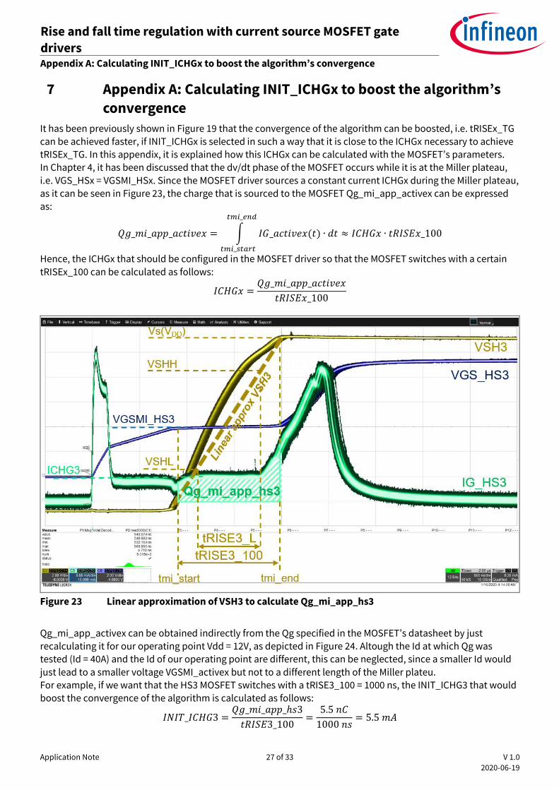
can be achieved faster, if INIT_ICHGx is selected in such a way that it is close to the ICHGx necessary to achieve tRISEx_TG. In this appendix, it is explained how this ICHGx can be calculated with the MOSFET’s parameters. In Chapter 4, it has been discussed that the dv/dt phase of the MOSFET occurs while it is at the Miller plateau,
i.e. VGS_HSx = VGSMI_HSx. Since the MOSFET driver sources a constant current ICHGx during the Miller plateau, as it can be seen in Figure 23, the charge that is sourced to the MOSFET Qg_mi_app_activex can be expressed
as:
𝑄𝑔_𝑚𝑖_𝑎𝑝𝑝_𝑎𝑐𝑡𝑖𝑣𝑒𝑥 = ∫ 𝐼𝐺_𝑎𝑐𝑡𝑖𝑣𝑒𝑥(𝑡) ∙ 𝑑𝑡
𝑡𝑚𝑖_𝑒𝑛𝑑
𝑡𝑚𝑖_𝑠𝑡𝑎𝑟𝑡
≈ 𝐼𝐶𝐻𝐺𝑥 ∙ 𝑡𝑅𝐼𝑆𝐸𝑥_100
Hence, the ICHGx that should be configured in the MOSFET driver so that the MOSFET switches with a certain
tRISEx_100 can be calculated as follows:
𝐼𝐶𝐻𝐺𝑥 =𝑄𝑔_𝑚𝑖_𝑎𝑝𝑝_𝑎𝑐𝑡𝑖𝑣𝑒𝑥
𝑡𝑅𝐼𝑆𝐸𝑥_100
Figure 23 Linear approximation of VSH3 to calculate Qg_mi_app_hs3
Qg_mi_app_activex can be obtained indirectly from the Qg specified in the MOSFET’s datasheet by just
recalculating it for our operating point Vdd = 12V, as depicted in Figure 24. Altough the Id at which Qg was tested (Id = 40A) and the Id of our operating point are different, this can be neglected, since a smaller Id would
just lead to a smaller voltage VGSMI_activex but not to a different length of the Miller plateu. For example, if we want that the HS3 MOSFET switches with a tRISE3_100 = 1000 ns, the INIT_ICHG3 that would boost the convergence of the algorithm is calculated as follows:
𝐼𝑁𝐼𝑇_𝐼𝐶𝐻𝐺3 =𝑄𝑔_𝑚𝑖_𝑎𝑝𝑝_ℎ𝑠3
𝑡𝑅𝐼𝑆𝐸3_100=
5.5 𝑛𝐶
1000 𝑛𝑠= 5.5 𝑚𝐴

Application Note 28 of 33 V 1.0
2020-06-19
Rise and fall time regulation with current source MOSFET gate
drivers Appendix A: Calculating INIT_ICHGx to boost the algorithm’s convergence
Thus, the constant INIT_ICHG3 should be set to 11, which corresponds to an ICHG3 of 5 mA according to the datasheet of the TLE956x.
Figure 24 Extrapolation of Qg_mi_app_hs3 for Vdd = 12 V
The value for the tRISE3_TG constant of our algorithm can be obtained from the desired tRISE3_100 by doing a linear approximation of VSH3 as depicted in Figure 23:
𝑡𝑅𝐼𝑆𝐸3_𝑇𝐺 = 𝑡𝑅𝐼𝑆𝐸3_𝐿 = (1 −𝑉𝑆𝐻𝐿 + (𝑉𝑠 − 𝑉𝑆𝐻𝐻)
𝑉𝑠) ∙ 𝑡𝑅𝐼𝑆𝐸3_100
𝑡𝑅𝐼𝑆𝐸3_𝑇𝐺 = (1 −2.25 𝑉 + 2.25 𝑉
12 𝑉) ∙ 1000 𝑛𝑠 = 625 𝑛𝑠
Since the MOSFET driver measures the tRISE3 with a granularity of 53.3 ns, the tRISE3_TG constant of the
algorithm should be set to 11:
𝑡𝑅𝐼𝑆𝐸3_𝑇𝐺 =625 𝑛𝑠
53.3 𝑛𝑠= 11
Application Note 29 of 33 V 1.0
2020-06-19
Rise and fall time regulation with current source MOSFET gate
drivers Appendix B: Source code EMA-based hysteresis algorithm
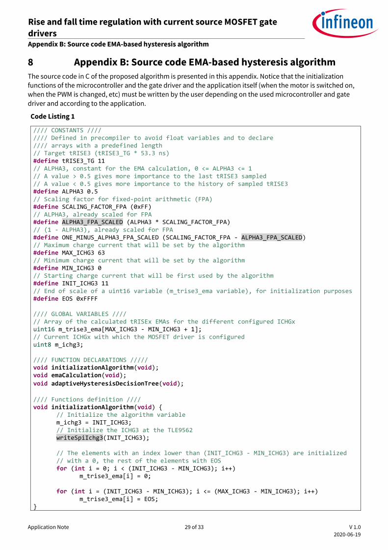
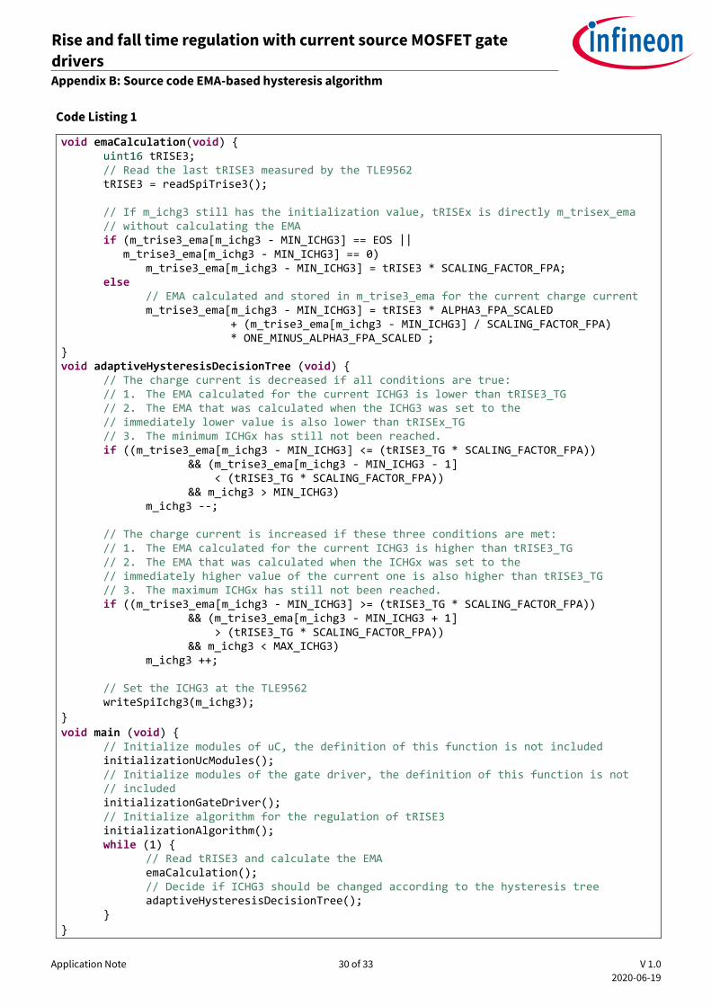
8 Appendix B: Source code EMA-based hysteresis algorithm
The source code in C of the proposed algorithm is presented in this appendix. Notice that the initialization functions of the microcontroller and the gate driver and the application itself (when the motor is switched on, when the PWM is changed, etc) must be written by the user depending on the used microcontroller and gate
driver and according to the application.
Code Listing 1
//// CONSTANTS //// //// Defined in precompiler to avoid float variables and to declare //// arrays with a predefined length // Target tRISE3 (tRISE3_TG * 53.3 ns) #define tRISE3_TG 11 // ALPHA3, constant for the EMA calculation, 0 <= ALPHA3 <= 1 // A value > 0.5 gives more importance to the last tRISE3 sampled // A value < 0.5 gives more importance to the history of sampled tRISE3 #define ALPHA3 0.5 // Scaling factor for fixed-point arithmetic (FPA) #define SCALING_FACTOR_FPA (0xFF) // ALPHA3, already scaled for FPA #define ALPHA3_FPA_SCALED (ALPHA3 * SCALING_FACTOR_FPA) // (1 - ALPHA3), already scaled for FPA #define ONE_MINUS_ALPHA3_FPA_SCALED (SCALING_FACTOR_FPA - ALPHA3_FPA_SCALED) // Maximum charge current that will be set by the algorithm #define MAX_ICHG3 63 // Minimum charge current that will be set by the algorithm #define MIN_ICHG3 0 // Starting charge current that will be first used by the algorithm #define INIT_ICHG3 11 // End of scale of a uint16 variable (m_trise3_ema variable), for initialization purposes #define EOS 0xFFFF //// GLOBAL VARIABLES //// // Array of the calculated tRISEx EMAs for the different configured ICHGx uint16 m_trise3_ema[MAX_ICHG3 - MIN_ICHG3 + 1]; // Current ICHGx with which the MOSFET driver is configured uint8 m_ichg3; //// FUNCTION DECLARATIONS ///// void initializationAlgorithm(void); void emaCalculation(void);
void adaptiveHysteresisDecisionTree(void);
//// Functions definition //// void initializationAlgorithm(void) { // Initialize the algorithm variable m_ichg3 = INIT_ICHG3; // Initialize the ICHG3 at the TLE9562 writeSpiIchg3(INIT_ICHG3); // The elements with an index lower than (INIT_ICHG3 - MIN_ICHG3) are initialized // with a 0, the rest of the elements with EOS for (int i = 0; i < (INIT_ICHG3 - MIN_ICHG3); i++) m_trise3_ema[i] = 0; for (int i = (INIT_ICHG3 - MIN_ICHG3); i <= (MAX_ICHG3 - MIN_ICHG3); i++) m_trise3_ema[i] = EOS; }
Application Note 30 of 33 V 1.0
2020-06-19
Rise and fall time regulation with current source MOSFET gate
drivers Appendix B: Source code EMA-based hysteresis algorithm
Code Listing 1
void emaCalculation(void) { uint16 tRISE3; // Read the last tRISE3 measured by the TLE9562 tRISE3 = readSpiTrise3(); // If m_ichg3 still has the initialization value, tRISEx is directly m_trisex_ema // without calculating the EMA if (m_trise3_ema[m_ichg3 - MIN_ICHG3] == EOS || m_trise3_ema[m_ichg3 - MIN_ICHG3] == 0) m_trise3_ema[m_ichg3 - MIN_ICHG3] = tRISE3 * SCALING_FACTOR_FPA; else // EMA calculated and stored in m_trise3_ema for the current charge current m_trise3_ema[m_ichg3 - MIN_ICHG3] = tRISE3 * ALPHA3_FPA_SCALED + (m_trise3_ema[m_ichg3 - MIN_ICHG3] / SCALING_FACTOR_FPA) * ONE_MINUS_ALPHA3_FPA_SCALED ; } void adaptiveHysteresisDecisionTree (void) { // The charge current is decreased if all conditions are true: // 1. The EMA calculated for the current ICHG3 is lower than tRISE3_TG // 2. The EMA that was calculated when the ICHG3 was set to the // immediately lower value is also lower than tRISEx_TG // 3. The minimum ICHGx has still not been reached. if ((m_trise3_ema[m_ichg3 - MIN_ICHG3] <= (tRISE3_TG * SCALING_FACTOR_FPA)) && (m_trise3_ema[m_ichg3 - MIN_ICHG3 - 1] < (tRISE3_TG * SCALING_FACTOR_FPA)) && m_ichg3 > MIN_ICHG3) m_ichg3 --; // The charge current is increased if these three conditions are met: // 1. The EMA calculated for the current ICHG3 is higher than tRISE3_TG // 2. The EMA that was calculated when the ICHGx was set to the // immediately higher value of the current one is also higher than tRISE3_TG // 3. The maximum ICHGx has still not been reached. if ((m_trise3_ema[m_ichg3 - MIN_ICHG3] >= (tRISE3_TG * SCALING_FACTOR_FPA)) && (m_trise3_ema[m_ichg3 - MIN_ICHG3 + 1] > (tRISE3_TG * SCALING_FACTOR_FPA)) && m_ichg3 < MAX_ICHG3) m_ichg3 ++; // Set the ICHG3 at the TLE9562 writeSpiIchg3(m_ichg3);
}
void main (void) { // Initialize modules of uC, the definition of this function is not included initializationUcModules(); // Initialize modules of the gate driver, the definition of this function is not // included initializationGateDriver(); // Initialize algorithm for the regulation of tRISE3 initializationAlgorithm(); while (1) { // Read tRISE3 and calculate the EMA emaCalculation(); // Decide if ICHG3 should be changed according to the hysteresis tree adaptiveHysteresisDecisionTree(); }
}

Application Note 31 of 33 V 1.0
2020-06-19
Rise and fall time regulation with current source MOSFET gate
drivers References
9 References
[1] Infineon Technologies AG: “TLE92108 / TLE92104 – Step-by-step MOSFET driver setting guide and calculator description”, Infineon Technologies AG, 2020.
[2] Schindler, Koeppl, Wicht: “EMC and switching loss improvement for fast switching power stages by di/dt, dv/dt optimization with 10 ns variable current source gate driver”, IEEE 10th international workshop on
EMC Compo, UK 2015.
[3] Ávila Herrera, Miura-Mattausch, Kikuchihara et al.: „Modeling of temperature-dependent MOSFET aging“, IEEE 2019.
[4] Schindler, Koeppl, Wicht: “10 ns variable current gate driver with control loop for optimized gate current timing and level control for in-transition slope shaping”, IEEE, 2017.
[5] Schindler, Koeppl, Wicht: “EMC analysis of current source gate drivers”, IEEE 9th international workshop on EMC Compo, Japan 2013.
[6] Clayton R. Paul: “Introduction to Electromagnetic Compatibility”, Wiley Interscience. ISBN 978-0-471-75500-5.
[7] Haynes, Corns, Kumar: “An exponential moving average algorithm”, IEEE WCCI, Australia 2012.

Application Note 32 of 33 V 1.0
2020-06-19
Rise and fall time regulation with current source MOSFET gate
drivers Revision history
Revision history
Document
version
Date of release Description of changes
V 1.0 Initial version
Trademarks All referenced product or service names and trademarks are the property of their respective owners.
Edition 2020-06-19
Z8F69449874
Published by
Infineon Technologies AG
81726 Munich, Germany
© 2020 Infineon Technologies AG.
All Rights Reserved.
Do you have a question about this
document?
Email: [email protected]
Document reference
IMPORTANT NOTICE The information contained in this application note is given as a hint for the implementation of the product only and shall in no event be regarded as a description or warranty of a certain functionality, condition or quality of the product. Before implementation of the product, the recipient of this application note must verify any function and other technical information given herein in the real application. Infineon Technologies hereby disclaims any and all warranties and liabilities of any kind (including without limitation warranties of non-infringement of intellectual property rights of any third party) with respect to any and all information given in this application note. The data contained in this document is exclusively intended for technically trained staff. It is the responsibility of customer’s technical departments to evaluate the suitability of the product for the intended application and the completeness of the product information given in this document with respect to such application.
For further information on the product, technology, delivery terms and conditions and prices please contact your nearest Infineon Technologies office (www.infineon.com).
WARNINGS Due to technical requirements products may contain dangerous substances. For information on the types in question please contact your nearest Infineon Technologies office. Except as otherwise explicitly approved by Infineon Technologies in a written document signed by authorized representatives of Infineon Technologies, Infineon Technologies’ products may not be used in any applications where a failure of the product or any consequences of the use thereof can reasonably be expected to result in personal injury.