RGB LED Controller Driver with PWM Control Ver.2012-07-31 - 1 - NJU6063V RGB LED Controller Driver...
30
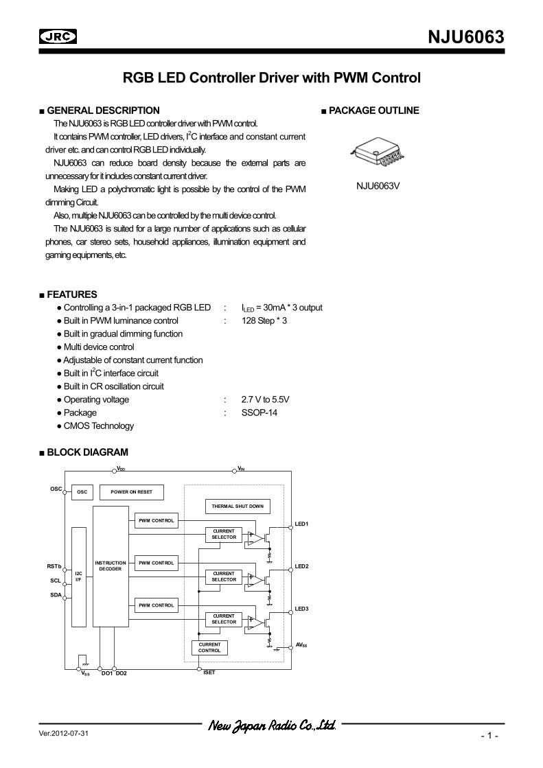
NJU6063 - 1 - Ver.2012-07-31 NJU6063V RGB LED Controller Driver with PWM Control ■ GENERAL DESCRIPTION ■ PACKAGE OUTLINE The NJU6063 is RGB LED controller driver with PWM control. It contains PWM controller, LED drivers, I 2 C interface and constant current driver etc. and can control RGB LED individually. NJU6063 can reduce board density because the external parts are unnecessary for it includes constant current driver. Making LED a polychromatic light is possible by the control of the PWM dimming Circuit. Also, multiple NJU6063 can be controlled by the multi device control. The NJU6063 is suited for a large number of applications such as cellular phones, car stereo sets, household appliances, illumination equipment and gaming equipments, etc. ■ FEATURES ● Controlling a 3-in-1 packaged RGB LED : I LED = 30mA * 3 output ● Built in PWM luminance control : 128 Step * 3 ● Built in gradual dimming function ● Multi device control ● Adjustable of constant current function ● Built in I 2 C interface circuit ● Built in CR oscillation circuit ● Operating voltage : 2.7 V to 5.5V ● Package : SSOP-14 ● CMOS Technology ■ BLOCK DIAGRAM LED1 LED3 AVSS I2C I/F OSC THERMAL SHUT DOWN SDA SCL RSTb DO1 OSC VDD V SS PWM CONTROL PWM CONTROL PWM CONTROL INSTRUCTION DECODER POWER ON RESET ISET CURRENT SELECTOR CURRENT SELECTOR CURRENT CONTROL VIN CURRENT SELECTOR LED2 DO2
Transcript of RGB LED Controller Driver with PWM Control Ver.2012-07-31 - 1 - NJU6063V RGB LED Controller Driver...
NJU6063
- 1 -Ver.2012-07-31
NJU6063V
RGB LED Controller Driver with PWM Control GENERAL DESCRIPTION PACKAGE OUTLINE
The NJU6063 is RGB LED controller driver with PWM control. It contains PWM controller, LED drivers, I2C interface and constant current
driver etc. and can control RGB LED individually. NJU6063 can reduce board density because the external parts are
unnecessary for it includes constant current driver. Making LED a polychromatic light is possible by the control of the PWM
dimming Circuit. Also, multiple NJU6063 can be controlled by the multi device control. The NJU6063 is suited for a large number of applications such as cellular
phones, car stereo sets, household appliances, illumination equipment and gaming equipments, etc.
FEATURES Controlling a 3-in-1 packaged RGB LED : ILED = 30mA * 3 output Built in PWM luminance control : 128 Step * 3 Built in gradual dimming function Multi device control Adjustable of constant current function Built in I2C interface circuit Built in CR oscillation circuit Operating voltage : 2.7 V to 5.5V Package : SSOP-14 CMOS Technology BLOCK DIAGRAM
LED1
LED3
AVSS
I2CI/F
OSC
THERMAL SHUT DOWN
SDA
SCL
RSTb
DO1
OSC
VDD
VSS
PWM CONTROL
PWM CONTROL
PWM CONTROL
INSTRUCTIONDECODER
POWER ON RESET
ISET
CURRENTSELECTOR
CURRENTSELECTOR
CURRENTCONTROL
VIN
CURRENTSELECTOR
LED2
DO2
NJU6063
- 2 - Ver.2012-07-31
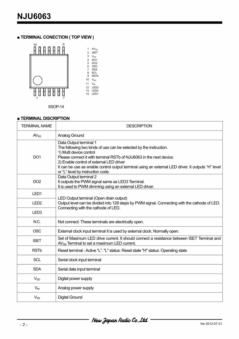
TERMINAL CONECTION ( TOP VIEW ) SSOP-14 TERMINAL DISCRIPTION
TERMINAL NAME DESCRIPTION
AVSS Analog Ground
DO1
Data Output terminal 1 The following two kinds of use can be selected by the instruction. 1) Multi device control Please connect it with terminal RSTb of NJU6063 in the next device. 2) Enable control of external LED driver It can be use as enable control output terminal using an external LED driver. It outputs “H” level or “L” level by instruction code.
DO2 Data Output terminal 2 It outputs the PWM signal same as LED3 Terminal. It is used to PWM dimming using an external LED driver.
LED1
LED2
LED3
LED Output terminal (Open drain output) Output level can be divided into 128 steps by PWM signal. Connecting with the cathode of LED.Connecting with the cathode of LED.
N.C. Not connect. These terminals are electrically open.
OSC External clock input terminal It is used by external clock. Normally open.
ISET Set of Maximum LED drive current. It should connect a resistance between ISET Terminal and AVSS Terminal to set a maximum LED current.
RSTb Reset terminal - Active “L”. "L" status: Reset state "H" status: Operating state
SCL Serial clock input terminal
SDA Serial data input terminal
VDD Digital power supply
VIN Analog power supply
VSS Digital Ground
1 AVSS
2 ISET3 VSS
4 DO15 DO26 OSC7 SDA8 SCL9 RSTb
10 VDD
11 VIN
12 LED313 LED214 LED1

NJU6063
- 3 -Ver.2012-07-31
ABSOLUTE MAXIMUMN RATINGS (Ta=25˚C)
PARAMETER SYMBOL RATING UNIT
Power supply 1 VDD - 0.3 ~ + 7.0 V
Power supply 2 VIN - 0.3 ~ + 7.0 V
Input voltage 1 VI1 - 0.3 ~ + 7.0 (*1) V
Input voltage 2 VI2 - 0.3 ~ + 7.0 (*2) V
Input voltage 3 VI3 - 0.3 ~ + 7.0 (*3) V
Input voltage 4 VI4 - 0.3 ~ + 7.0 (*4) V
Output current 1 ILED 0 ~ 60 (*1) mA
Output current 2 IDO 5 (*5) mA
Power dissipation PD 450 (*6) 570 (*7) mW
Operating temperature Topr - 40 ~ + 85 °C
Storage temperature Tstg - 55 ~ + 125 °C Note) VSS = AVSS = 0 V to all condition *1) It applies to the terminal LED1, LED2 and LED3. *2) It applies to the terminal ISET. When the power supply voltage less than 7V, it becomes equal with power supply voltage 2. *3) It applies to the terminal RSTb and OSC. *4) It applies to the terminal SCL and SDA. *5) It applies to the terminal DO1and DO2. *6) Mounted on glass epoxy board. (76.2×114.3×1.6mm:EIA/JDEC standard size, 2Layers) *7) Mounted on glass epoxy board. (76.2×114.3×1.6mm:EIA/JDEC standard size, 4Layers) RECOMMENDED OPERATING CONDITION (Ta=25˚C)
PARAMETER SYMBOL CONDITIONS MIN. TYP. MAX UNIT
Logic power supply voltage VDD 1.8 3.0 5.5 V
Analog power supply voltage VIN 2.7 3.0 5.5 V
Input voltage VLED - - 5.5 V

NJU6063
- 4 - Ver.2012-07-31
ELECTRICAL CHARACTERISTICS ( VDD = 3.0V, VIN = 3.0V, RSTb = VDD, RISET = 3.3kΩ, Ta=25˚C )
PARAMETER SYMBOL CONDITIONS MIN. TYP. MAX. UNIT
< INPUT BLOCK >
Input “H” level voltage 1 VIH1 SCL, SDA 0.7VDD - VDD V
Input “H” level voltage 2 VIH2 RSTb, OSC 0.8VDD - VDD V
Input “L” level voltage 1 VIL1 SCL, SDA 0 - 0.3VDD V
Input “L” level voltage 2 VIL2 RSTb, OSC 0 - 0.2VDD V
Input “H” level current IIH RSTb, OSC, SCL, SDA, VI = VDD When the OSC terminal is measured, initialization is 02H.
- - 0.3 µA
Input “L” level current IIL RSTb, OSC, SCL, SDA, VI = 0V When the OSC terminal is measured, initialization is 02H.
- 0.3 - - µA
Pull up resistance current IRUP OSC, Initialization = 00h, VI = 0V - 8 12 µA
< OSCILLATION BLOCK >
fOSC(1) FC1 = 0, FC0 = 0 0.7 1 1.3
fOSC(2) FC1 = 0, FC0 = 1 0.91 1.3 1.69
fOSC(3) FC1 = 1, FC0 = 0 1.54 2.2 2.86Oscillation frequency
fOSC(4) FC1 = 1, FC0 = 1 0.56 0.8 1.04
MHz
External clock maximum frequency fEX OSC - - 5 MHz
Clock pulse width ” L ” tEXL OSC 100 - - ns
Clock pulse width ” H ” tEXH OSC 100 - - ns
Rise time 3 tr3 OSC - - 300 ns
Fall time 3 tf3 OSC - - 300 ns
Maximum frame frequency fFRAME LED1, LED2, LED3, Setting of current magnification = 100% PWM setting = 01h, FD1 = 0, FD0 = 0
- - 5.23 kHz
< GENERAL CHARACTERISTICS >
Operating current 1 IOP1 VDD, Initialization = 01h, LED1 ~ LED3 PWM Setting = 00h, VI1 = 2V - 160 240 µA
Operating current 2 IOP2
VIN, Initialization = 01h, Setting of current magnification = 100% LED1 ~ LED3 PWM Setting = 00h, Static ON = 00h, VI1 = 2V
- 660 760 µA
Operating current at OFF state 1 INOP1 VDD, Initialization = 00h, VI1 = 2V - 2.3 3.9 µA
Operating current at OFF state 2 INOP2 VIN, Initialization = 00h, VI1 = 2V - - 1 µA

NJU6063
- 5 -Ver.2012-07-31
ELECTRICAL CHARACTERISTICS ( VDD = 3.0V, VIN = 3.0V, RSTb = VDD, RISET = 3.3kΩ, Ta=25˚C )
PARAMETER SYMBOL CONDITIONS MIN. TYP. MAX. UNIT
< OUTPUT BLOCK >
Output “H” level voltage 1 VOH1 DO1, IO = - 0.1mA 0.8VDD - - V
Output “L” level voltage 1 VOL1 DO1, IO = 0.1mA - - 0.2VDD V
Output “H” level voltage 2 VOH2 DO2, IO = - 0.1mA 0.8VDD - - V
Output “L” level voltage 2 VOL2 DO2, IO = 0.1mA - - 0.2VDD V
Output “L” level voltage 3 VOL3 SDA, IO = 3mA - - 0.4 V
< LED DRIVE BLOCK >
OFF leakage current 1 ILED_OFFH1 LED1, VI1 = 5.5V
OFF leakage current 2 ILED_OFFH2 LED2, VI1 = 5.5V
OFF leakage current 3 ILED_OFFH3 LED3, VI1 = 5.5V
- - 0.3 µA
Drive current 1 ILED1 LED1, setting of current magnification = 100%
Drive current 2 ILED2 LED2, setting of current magnification = 100%
Drive current 3 ILED3 LED3, setting of current magnification = 100%
29.1 30.3 31.5 mA
Drive current matching 1 IMLED1 ( ILED1 – ILED_AVG ) / ILED_AVG * 100 ILED_AVG = ( ILED1 + ILED2 + ILED3 ) / 3 setting of current magnification = 100%
Drive current matching 2 IMLED2 ( ILED2 – ILED_AVG ) / ILED_AVG * 100 ILED_AVG = ( ILED1 + ILED2 + ILED3 ) / 3 setting of current magnification = 100%
Drive current matching 3 IMLED3 ( ILED3 – ILED_AVG ) / ILED_AVG * 100 ILED_AVG = ( ILED1 + ILED2 + ILED3 ) / 3 setting of current magnification = 100%
- 1.7 - 1.7 %
LED terminal saturation voltage 1 VLED_SAT1
LED1, ILED1=28mA, setting of current magnification = 100%
LED terminal saturation voltage 2 VLED_SAT2
LED2, ILED2=28mA, setting of current magnification = 100%
LED terminal saturation voltage 3 VLED_SAT3
LED3, ILED3=28mA, setting of current magnification = 100%
- - 0.65 V
< OUTPUT TIMING >
Output delay time tDC DO1, CL = 10pF - - 300 ns
< RESET TIMING >
RESET “L” pulse width tRW RSTb 400 - - ns
RESET time tR RSTb 1 - - µs
Rise time 2 tr2 RSTb - - 300 ns
Fall time 2 tf2 RSTb - - 300 ns

NJU6063
- 6 - Ver.2012-07-31
ELECTRICAL CHARACTERISTICS ( VDD = 3.0V, VIN = 3.0V, RSTb = VDD, RISET = 3.3kΩ, Ta=25˚C )
PARAMETER SYMBOL CONDITIONS MIN. TYP. MAX. UNIT
< MULTI DEVICE ACCESS TIMING >
Access time of multi device control tMA SDA, DO1 4.5 - - µs
< I2C BUS TIMING ( VDD = 3.0V, High Speed Mode ) >
SCL clock frequency fSCL SCL - - 400 kHz
Hold time for repeated START condition tHD;STA SCL, SDA 0.6 - - µs
SCL clock “ L ” tLOW SCL 1.3 - - µs
SCL clock “ H ” tHIGH SCL 0.6 - - µs
Setup time for repeated START condition tSU;STA SCL, SDA 0.6 - - µs
Data hold time tHD;DAT SCL, SDA 0 - 0.9 µs
Data setup time tSU;DAT SCL, SDA 100 - - ns
Rise time tr1 SCL, SDA - - 300 ns
Fall time tf1 SCL, SDA - - 300 ns
Setup time for STOP condition tSU;STO SCL, SDA 0.6 - - µs
Bus free time between STOP and START condition tBUF SDA 1.3 - - µs
< I2C BUS TIMING ( VDD = 1.8V, NORMAL Mode ) >
SCL clock frequency fSCL SCL - - 100 kHz
Hold time for repeated START condition tHD;STA SCL, SDA 4.0 - - µs
SCL clock “ L ” tLOW SCL 4.7 - - µs
SCL clock “ H ” tHIGH SCL 4.0 - - µs
Setup time for repeated START condition tSU;STA SCL, SDA 4.7 - - µs
Data hold time tHD;DAT SCL, SDA 0 - 3.45 µs
Data setup time tSU;DAT SCL, SDA 250 - - ns
Rise time tr1 SCL, SDA - - 1000 ns
Fall time tf1 SCL, SDA - - 300 ns
Setup time for STOP condition tSU;STO SCL, SDA 4.0 - - µs
Bus free time between STOP and START condition tBUF SDA 4.7 - - µs

NJU6063
- 7 -Ver.2012-07-31
(1) I2C Bus Timing
S : START Condition Sr : Repetition START Condition P : STOP Condition (2) RESET Timing
(3) Multi Device Access Timing - Setting of Upper Address
(4) External Clock
FUNCTIONAL DESCRIPTIONS
SDA
SCL
tf1tSU;DAT
S tHD;STA
tLOW tr1
tHD;DAT tHIGH
tf1
tSU;STA Sr
tHD;STA
tSU;STOP
tBUF
S
tr1
RSTb
SDA
tRW tR
tr2tf2
SDA
SCL1 8 9
tDC
tMA
DO1
tf3
OSC
tEXL
tEX tEXH
LED
fFRAME
tr3
NJU6063
- 8 - Ver.2012-07-31
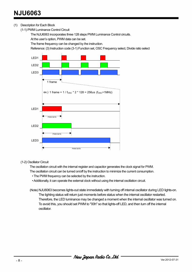
(1) Description for Each Block (1-1) PWM Luminance Control Circuit The NJU6063 incorporates three 128 steps PWM Luminance Control circuits. At the user’s option, PWM data can be set. The frame frequency can be changed by the instruction. Reference: (3) Instruction code (3-1) Function set, OSC Frequency select, Divide ratio select
(1-2) Oscillator Circuit The oscillation circuit with the internal register and capacitor generates the clock signal for PWM. The oscillation circuit can be turned on/off by the instruction to minimize the current consumption. • The PWM frequency can be selected by the instruction. • Additionally, it can operate the external clock without using the internal oscillation circuit. (Note) NJU6063 becomes lights-out state immediately with turning off internal oscillator during LED lights-on. The lighting status will return just moments before status when the internal oscillator restarted. Therefore, the LED luminance may be changed a moment when the internal oscillator was turned on. To avoid this, you should set PWM to "00h" so that lights-off LED, and then turn off the internal oscillator.
LED1
LED2
LED3
(fOSC=1MHz)
PWM DATA
LED1
LED2
LED3
PWM DATA
PWM DATA
1 frame
ex.) 1 frame = 1 / fOSC * 2 * 128 = 256us
NJU6063
- 9 -Ver.2012-07-31
(1-3) LED Luminance Control Setting There are the following three methods of LED Luminance setting. (a) Setting of maximum LED current with ISET Terminal (LED1∼3 common setting) (b) LED Current Magnification Setting (LED1∼3 Separate setting) (c) PWM Signal Setting (LED 1∼3 Separate setting) (a) Setting of maximum LED current with ISET Terminal (LED1∼3 common setting) The setting of maximum LED current connects resistance between the terminal ISET and the terminal AVSS. The Maximum LED current range can be set in the 5mA to 10mA range.
ISETISET
LED RRVtimesI 100][5.0][200
=×
= (Ex. ILED(MAX)=30.3mA setting, RISET=3.3kΩ)
The LED drive transistor is turned off and the LED driving current is intercepted when ISET Terminal and AVSS Terminal are short-circuited. (b) LED Current Magnification Setting (LED1∼3 Separate setting) The LED current of each LED Terminal can be set the following three magnification: one time, one harf and one-quarter against ILED(MAX) that set by RISET. The I2C instruction can set this setting. Refer to (3) Instruction code: (3-2) LED current setting in detail. (c) PWM Signal Setting (LED 1∼3 Separate setting) The PWM signal of each LED terminal is set according to the instruction. PWM Duty can divide between 0% to 100% into 128. Refer to (3) Instruction code: (3-3) PWM setting in details. (1-4) Multi Device Function
NJU6063 can control multi device (a number of NJU6063) on I2C bus line. Refer to (7) Multi Device Control in details. (1-5) PWM Data Output Function The PWM data is output as CMOS output that set to LED3 from DO2 Terminal. The PWM data is waveform inverted of LED3 Terminal output and this output control is same as LED3 setting. Moreover, the large current drive LED port can be added by connecting the DO2 Terminal to NJU6080 PWM terminal.
NJU6063
- 10 - Ver.2012-07-31
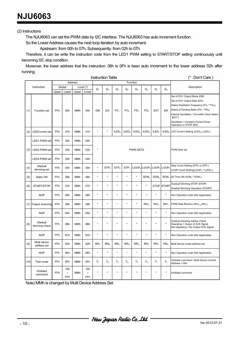
(2) Instructions The NJU6063 can set the PWM data by I2C interface. The NJU6063 has auto increment function. So the Lower Address causes the next loop iteration by auto increment. Apstream: from 00h to 07h, Subsequently: from 02h to 07h Therefore, it can be write the instruction code from the LED1 PWM setting to START/STOP setting continuously until becoming I2C stop condition. Moreover, the lower address that the instruction: 08h to 0Fh is been auto increment to the lower address 02h after running.
Instruction Table (* : Don’t Care )
Note) MMh is changed by Multi Device Address Set.
Upper Lower Upper LowerSet of DO1 Output Mode (DM)
Set of DO1 Output Data (DO)
Select Oscillation Frequency (FC1~FC0)
Select of Dividing Ratio (FD1~FD0)
Internal Oscillation / Out width Clock Select(EXT)
Oscillation / Constant Current DriverOperation or STOP (EN)
(2) LEDCurrent set FFh 01h MMh 01h * * ILED5 ILED4 ILED3 ILED2 ILED1 ILED0 LED Current Setting (ILED5 to ILED1)
LED1 PWM set FFh 02h MMh 02h
LED2 PWM set FFh 03h MMh 03h
LED3 PWM set FFh 04h MMh 04h
Step Count Setting (STP3 to STP1)
LOOP Count Setting(LOOP4~LOOP1)
(5) Static ON FFh 06h MMh 06h * * * * * SON3 SON2 SON1 All Time ON (SON3~SON1)
Gradual Dimming STOP (STOP)
Gradual Dimming Operation (START)
NOP FFh 08h MMh 08h * * * * * * * * Non Operation code (Not Applicable)
(7) Output reversing FFh 09h MMh 09h * * * * * INV3 INV2 INV1 PWM Data Reverce (INV3 to INV1)
NOP FFh 0Ah MMh 0Ah * * * * * * * * Non Operation code (Not Applicable)
(8) Gladualdimming check FFh 0Bh MMh 0Bh * * * * * * * *
Gradual Dimming Addles CheckOperating = Output of ACK SignalNot Operating = No Output ACK Signal
NOP FFh 0Ch MMh 0Ch * * * * * * * * Non Operation code (Not Applicable)
NOP FFh 0Eh MMh 0Eh * * * * * * * * Non Operation code (Not Applicable)
(10) Test mode FFh 0Fh MMh 0Fh T7 T6 T5 T4 T3 T2 T1 T0Inhibited command / Multi Device ControlAddress = 00h
10h 10h~ ~
FFh FFh
MMh STOP*
D6
MA3
FC0 FD1
D3
PWM DATA
MA0
START
DO FC1
MMh 0Dh MA1MA7 MA6(9) Multi deviceaddless set FFh 0Dh Multi Device mode address set
Inhibitedcommand FFh MMh * *
MA5 MA4 MA2
** * * **
* * *(6) START/STOP FFh 07h 07h *
LOOP4 LOOP3*
*
05h STP3 STP2 STP1(4) FFh 05h MMhGladualdimming set
LOOP1
PWM Data set
EXT
LOOP2
MMh 00h
(3) *
Instruction
Address
DM
Inhibited command
(1) Function set FFh 00h ENFD0
DescriptionGlobal Local (*)D7 D5 D4 D2 D1 D0
Function
NJU6063
- 11 -Ver.2012-07-31
<Instruction Code Example>
INSTRUCTION DATA REMARKS
I2C START Condition
SLAVE ADDRESS 40h Slave Address od Device
UPPER ADDRESS 00h Multi Device Address
LOWER ADDRESS 00h Address of Internal Resistor
INITIAL SETTING 01h Initialization of oscillation etc.
LED CURRENT SETTING 3Fh Magnification setting of LED current
LED1 PWM SETTING 10h
LED2 PWM SETTING 10h
LED3 PWM SETTING 10h
GRADUAL DIMMING SETTING 31h Setting of STEP(8) and LOOP(8)
STATIC ON 00h Setting of All Time ON
START/STOP 01h START of Gradual Dimming
wait (19ms)
LED1 PWM SETTING 20h
LED2 PWM SETTING 20h
LED3 PWM SETTING 20h
GRADUAL DIMMING SETTING 43h Setting of STEP(16) and LOOP(16)
STATIC ON 00h Setting of All Time ON
START/STOP 01h START of Gradual Dimming
wait (70ms)
LED1 PWM SETTING 40h
LED2 PWM SETTING 40h
LED3 PWM SETTING 40h
GRADUAL DIMMING SETTING 43h Setting of STEP(8) and LOOP(4)
STATIC ON 00h Setting of All Time ON
START/STOP 01h START of Gradual Dimming
I2C STOP Condition
START CONDITION
PWM DATA Setting
PWM DATA Re Setting
PWM DATA Setting
STOP CONDITION
NJU6063
- 12 - Ver.2012-07-31
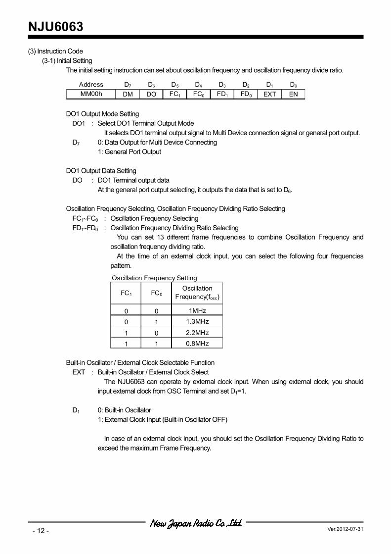
(3) Instruction Code (3-1) Initial Setting The initial setting instruction can set about oscillation frequency and oscillation frequency divide ratio.
DO1 Output Mode Setting DO1 : Select DO1 Terminal Output Mode It selects DO1 terminal output signal to Multi Device connection signal or general port output. D7 0: Data Output for Multi Device Connecting 1: General Port Output DO1 Output Data Setting DO : DO1 Terminal output data At the general port output selecting, it outputs the data that is set to D6. Oscillation Frequency Selecting, Oscillation Frequency Dividing Ratio Selecting FC1∼FC0 : Oscillation Frequency Selecting FD1∼FD0 : Oscillation Frequency Dividing Ratio Selecting You can set 13 different frame frequencies to combine Oscillation Frequency and oscillation frequency dividing ratio. At the time of an external clock input, you can select the following four frequencies pattern.
Built-in Oscillator / External Clock Selectable Function EXT : Built-in Oscillator / External Clock Select The NJU6063 can operate by external clock input. When using external clock, you should input external clock from OSC Terminal and set D1=1. D1 0: Built-in Oscillator 1: External Clock Input (Built-in Oscillator OFF) In case of an external clock input, you should set the Oscillation Frequency Dividing Ratio to exceed the maximum Frame Frequency.
D7 D6 D5 D4 D3 D2 D1 D0
DM DO FC1 FC0 FD1 FD0 EXT ENAddressMM00h
Oscillation Frequency Setting
FC1 FC0
0 00 1
1 01 1 0.8MHz
OscillationFrequency(fosc)
1MHz1.3MHz
2.2MHz

NJU6063
- 13 -Ver.2012-07-31
Oscillation Frequency Dividing Ratio and Frame Frequency Example
Enable Function EN : Enable / Disable Selecting The LED13 output stops by common setting. The built-in oscillation circuit stops at disable. The I2C interface is operating. D0 0: Disable (Stop LED1∼3 output (Turn OFF)) 1: Enable (3-2) LED Current Setting The LED driving current magnification can be set by LED Current Setting instruction.
It selects the LED current from the following three (3) magnifications: 1 time, 0.5 times and 0.25 times
LED1 Terminal Adjustment Example
Regarding ILED2, ILED3 and ILED4, ILED5 setting, same specifications as above.
fosc=1MHz fosc=1.3MHz fosc=2.2MHz fosc=0.8MHz
fOSC
2×1×128
fOSC
2×2×128
fOSC
2×4×128
fOSC
2×8×1280.5kHz 0.6kHz 1.1kHz 0.4kHz
1.0kHz 1.3kHz 2.1kHz 0.8kHz
2.0kHz 2.5kHz 1.6kHz
3.9kHz 3.1kHz
1
0
1
00
0
1
1
FD1 FD0Example Frame OscillationFrame
Oscillation
Frame Frequency1/128step
Frame signal( Signal Internal IC )
fosc = 1MHz, FD1 = 0, FD0 = 0 Set
Frame Frequency = fosc / 2 * 1 * 128 = 3.9kHz
Frame Cycle = 1/ fosc * 2 * 128 = 256 us
Minimum PWM Width = Frame Cycle / 128 = 2us
D7 D6 D5 D4 D3 D2 D1 D0
* * ILED5 ILED4 ILED3 ILED2 ILED1 ILED0MM01hAddress
ILED0、ILED1 Output current magnification adjustment of LED1 terminal
ILED2、ILED3 Output current magnification adjustment of LED2 terminal
ILED4、ILED5 Output current magnification adjustment of LED3 terminal
ILED1 ILED0LED Magnificationof Driving Current REMARK
0 0 ILED x 0 LED Driver OFF (Turn off)0 1 ILED x 0.251 0 ILED x 0.51 1 ILED x 1

NJU6063
- 14 - Ver.2012-07-31
(3-3) PWM Setting
It sets the PWM data that is output to the LED1∼3 Terminal. The PWM data can be set the PWM output of 128 step from 0 to 127.
128128
can be set by <Static ON> instruction.
PWM Data Setting Example
PWM DUTY corresponding to PWM Data Example
D7 D6 D5 D4 D3 D2 D1 D0
***
LED1 Terminal PWM dataAddressMM02hMM03h LED2 Terminal PWM dataMM04h LED3 Terminal PWM data
1 Frame ( 128 )
PWM DATA
PWM DATA
PWM DATA
LED1
LED2
LED3
PWM 7 PWM 6 PWM 5 PWM 4 PWM 3 PWM 2 PWM 1 PWM 0 PWM DUTY
1
1
0 1
0
11
1
1 1
1
1
1
1
1
1
1
1
*
*
*
1
1
1
0 0 1 0
0*
0 0*
1000
* 0 0 0 0 0 1 1
0
0 0 0 0
0*
* 0
0000
0
1
0 0 0 0
10
1 0
* 0 0 0128
0
1281
1282
1283
1284
1285
128125
128126
128127

NJU6063
- 15 -Ver.2012-07-31
(3-4) Gradual Dimming Setting It can be set Gradual Dimming Luminance Timing Setting.
The Gradual Dimming is a function that changes it while interpolating the middle data to the PWM data newly set from the PWM data that has already been set. The Gradual Dimming Setting instruction sets the following condition: - The step of number the intermediate data interpolation. - The loop count of each step. These setting detail are as follows. STEP Number Setting
LOOP Number Setting
D7 D6 D5 D4 D3 D2 D1 D0
* STP3 STP2 STP1 LOOP4 LOOP3 LOOP2 LOOP1
Address
MM05h
STP3 STP2 STP1 STEP Count0 0 0 1
0 0 1 2
0 1 0 40 1 1 8
1 0 0 161 0 1 32
1 1 0 Prohibit Set ( STEP Count = 1 )
1 1 1 Prohibit Set ( STEP Count = 1 )
LOOP4 LOOP3 LOOP2 LOOP1 LOOP Count0 0 0 0 4
0 0 0 1 8
0 0 1 0 120 0 1 1 16
0 1 0 0 200 1 0 1 24
0 1 1 0 280 1 1 1 32
1 0 0 0 361 0 0 1 40
1 0 1 0 44
1 0 1 1 481 1 0 0 52
1 1 0 1 561 1 1 0 60
1 1 1 1 64
NJU6063
- 16 - Ver.2012-07-31
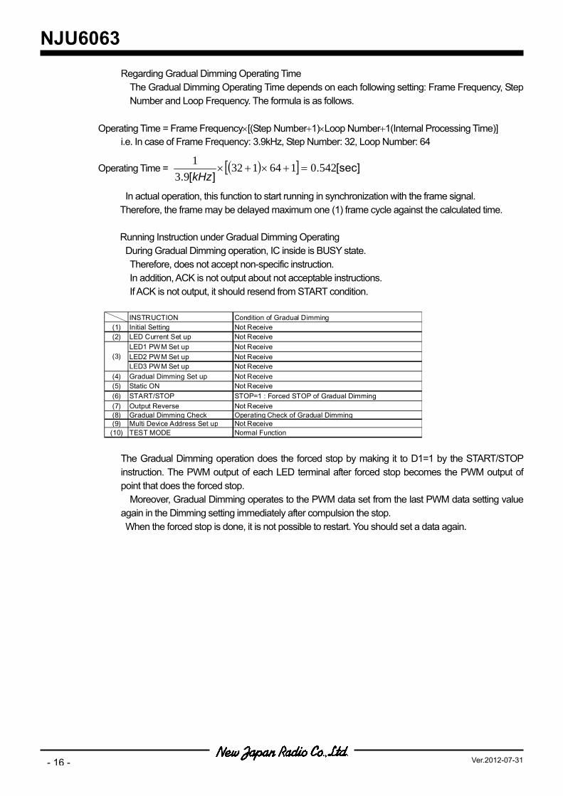
Regarding Gradual Dimming Operating Time The Gradual Dimming Operating Time depends on each following setting: Frame Frequency, Step Number and Loop Frequency. The formula is as follows.
Operating Time = Frame Frequency×[(Step Number+1)×Loop Number+1(Internal Processing Time)] i.e. In case of Frame Frequency: 3.9kHz, Step Number: 32, Loop Number: 64
Operating Time = ( )[ ] [sec].][.
542016413293
1=+×+×
kHz
In actual operation, this function to start running in synchronization with the frame signal. Therefore, the frame may be delayed maximum one (1) frame cycle against the calculated time.
Running Instruction under Gradual Dimming Operating
During Gradual Dimming operation, IC inside is BUSY state. Therefore, does not accept non-specific instruction. In addition, ACK is not output about not acceptable instructions. If ACK is not output, it should resend from START condition.
The Gradual Dimming operation does the forced stop by making it to D1=1 by the START/STOP instruction. The PWM output of each LED terminal after forced stop becomes the PWM output of point that does the forced stop.
Moreover, Gradual Dimming operates to the PWM data set from the last PWM data setting value again in the Dimming setting immediately after compulsion the stop.
When the forced stop is done, it is not possible to restart. You should set a data again.
INSTRUCTION Condition of Gradual Dimming(1) Initial Setting Not Receive(2) LED Current Set up Not Receive
LED1 PWM Set up Not ReceiveLED2 PWM Set up Not ReceiveLED3 PWM Set up Not Receive
(4) Gradual Dimming Set up Not Receive(5) Static ON Not Receive(6) START/STOP STOP=1 : Forced STOP of Gradual Dimming(7) Output Reverse Not Receive(8) Gradual Dimming Check Operating Check of Gradual Dimming(9) Multi Device Address Set up Not Receive
(10) TEST MODE Normal Function
(3)

NJU6063
- 17 -Ver.2012-07-31
After the forced stop during Gradual Dimming operation, it isshown the PWM data variant output from LED Terminal to 00hwhen Gradual Dimming is re-operated.
Gradual Dimming Setting Example (Loop Number: 4, Step Number: 2 setting)
At normal function At forced STOP (3-5) Static ON
It can be set Static ON (PWM Duty128128
= ).
Static ON Function SON3∼SON1: LED3∼LED1 always-on setting The PWM data becomes invalid by making the SON1∼SON3 bit "H" for each LED Terminal,
and the output always turns on (128128
PWM Duty).
It should make the SON1∼SON3 bit "L" so that the PWM data effective, and set the PWM
pulse width to 00h when you always turn off (128
0PWM Duty) each LED Terminal.
Moreover, all LED Terminals can be made “H” (Turn OFF) by making EN=0 the initialization instruction. It corresponds to SON1=LED1, SON2=LED2, and SON3=LED3. After the Gradual Dimming operation is completed, the Static ON operation is executed. The Static ON the operation and the instruction setting example are shown on next page.
PWM
t00h
7Fh
Start ofGradualDimming
Finish ofGradualDimming
1 Frame
LED DATA ( Initial value )
LED1
1 Frame 1 Frame 1 Frame
Set of LOOP ( repeat )
1 Frame 1 Frame
Set of LOOP ( repeat )
Set of Step = 2
Interpolation valueInterpolation valueLED DATA ( Initial value )
4 Frame 4 Frame
LED DATA ( Set point ) LED DATA ( Set point )
4 Frame
LED DATA ( Initial value )
1 Frame
Internal processing time
PWM
t00h
Start ofGradual
Dimming
Force STOPof GradualDimming
7Fh
Start ofGradualDimming
D7 D6 D5 D4 D3 D2 D1 D0
* * * * * SON3 SON2 SON1
AddressMM06h

NJU6063
- 18 - Ver.2012-07-31
Static ON Operation Example1
Static ON Operation Example2
Set of Instruction 1Number of step = 8
Loop of step = 8Static ON = ON
Set of Instruction 2Number of step = 1
Loop of step = 8Static ON = OFF
00h( 0/128Duty)
SON(128/128Duty)
50h(80/128Duty)8 Frame
END ofStatic OFF
Gradual Dimming OperationGradual Dimming Operation Time
PWM DATA
tStart ofGradualDimming
Stop ofGradualDimming
END ofStatic ON
Start ofGradualDimming
Stop ofGradualDimming
77h(119/128Duty)
7Fh(127/128Duty)
Start ofGradualDimming
Stop ofGradual
Dimming
SON(128/128Duty)
END ofStatic ON
8 FRAME
Start ofGradualDimming
Start ofGradualDimming
8 FRAME
Set of Instruction 1Number of step = 8
Loop of step = 8Static ON = ON
Set of Instruction 2Number of step = 1
Loop of step = 8Static ON = OFF
Set of Instruction 3Number of step = 8
Loop of step = 8Static ON = OFF
PWM DATA
End ofGradualDimming
Gradual Dimming Operation Time
Stop ofGradualDimming
t
INSTRUCTION DATA REMARKS
START CONDITION I2C START Condition
SLAVE ADDRESS 40h Slave Address od DeviceUPPER ADDRESS 00h Multi Device Address
LOWER ADDRESS 00h Address of Internal ResistorINITIAL SETTING 01h Initialization of oscillation etc.
LED CURRENT SETTING 3Fh Magnification setting of LED currentLED1 PWM SETTING 00h
LED2 PWM SETTING 00hLED3 PWM SETTING 00h
GRADUAL DIMMING SETTING 00h Setting of STEP(1) and LOOP(4)
STATIC ON 00h Setting of All Time ONSTART/STOP 01h START of Gradual Dimming
wait (3ms)LED1 PWM SETTING 50h
LED2 PWM SETTING 50hLED3 PWM SETTING 50h
GRADUAL DIMMING SETTING 30h Setting of STEP(8) and LOOP(4)STATIC ON 07h Setting of All Time ON
START/STOP 01h START of Gradual Dimming
wait (10ms)STOP CONDITION I2C STOP Condition
START CONDITION I2C START ConditionSLAVE ADDRESS 40h Slave Address od Device
UPPER ADDRESS 00h Multi Device AddressLOWER ADDRESS 06h Address of Internal Resistor
STATIC ON 00h Setting of All Time ONSTART/STOP 01h START of Gradual Dimming
INSTRUCTIONSETTING 1
PWM DATA Setting
INSTRUCTIONSETTING 2
INITIAL SETTING
PWM DATA Setting
Static ON Explanation of Instruction Code (1)INSTRUCTION DATA REMARKS
START CONDITION I2C START Condition
SLAVE ADDRESS 40h Slave Address od DeviceUPPER ADDRESS 00h Multi Device Address
LOWER ADDRESS 00h Address of Internal ResistorINITIAL SETTING 01h Initialization of oscillation etc.
LED CURRENT SETTING 3Fh Magnification setting of LED currentLED1 PWM SETTING 77h
LED2 PWM SETTING 77hLED3 PWM SETTING 77h
GRADUAL DIMMING SETTING 00h Setting of STEP(1) and LOOP(4)
STATIC ON 00h Setting of All Time ONSTART/STOP 01h START of Gradual Dimming
wait (3ms)LED1 PWM SETTING 7Fh
LED2 PWM SETTING 7FhLED3 PWM SETTING 7Fh
STEP / TIME 30h Setting of STEP(8) and LOOP(4)STATIC ON 07h Setting of All Time ON
START/STOP 01h START of Gradual Dimming
wait (10ms)STOP CONDITION I2C STOP Condition
START CONDITION I2C START ConditionSLAVE ADDRESS 40h Slave Address od Device
UPPER ADDRESS 00h Multi Device AddressLOWER ADDRESS 05h Address of Internal Resistor
GRADUAL DIMMING SETTING 00h Setting of STEP(1) and LOOP(4)STATIC ON 00h Setting of All Time ON
START/STOP 01h START of Gradual Dimming
wait (3ms)STOP CONDITION I2C STOP Condition
START CONDITION I2C START ConditionSLAVE ADDRESS 40h Slave Address od Device
UPPER ADDRESS 00h Multi Device AddressLOWER ADDRESS 02h Address of Internal Resistor
LED1 PWM SETTING 77h
LED2 PWM SETTING 77hLED3 PWM SETTING 77hGRADUAL DIMMING SETTING 30h Setting of STEP(8) and LOOP(4)STATIC ON 00h Setting of All Time ONSTART/STOP 01h START of Gradual Dimming
PWM DATA Setting
INSTRUCTIONSETTING 2
INSTRUCTIONSETTING 1
PWM DATA Setting
INSTRUCTIONSETTING 3
INITIAL SETTING
PWM DATA Setting
Static ON Explanation of Instruction Code (2)
NJU6063
- 19 -Ver.2012-07-31
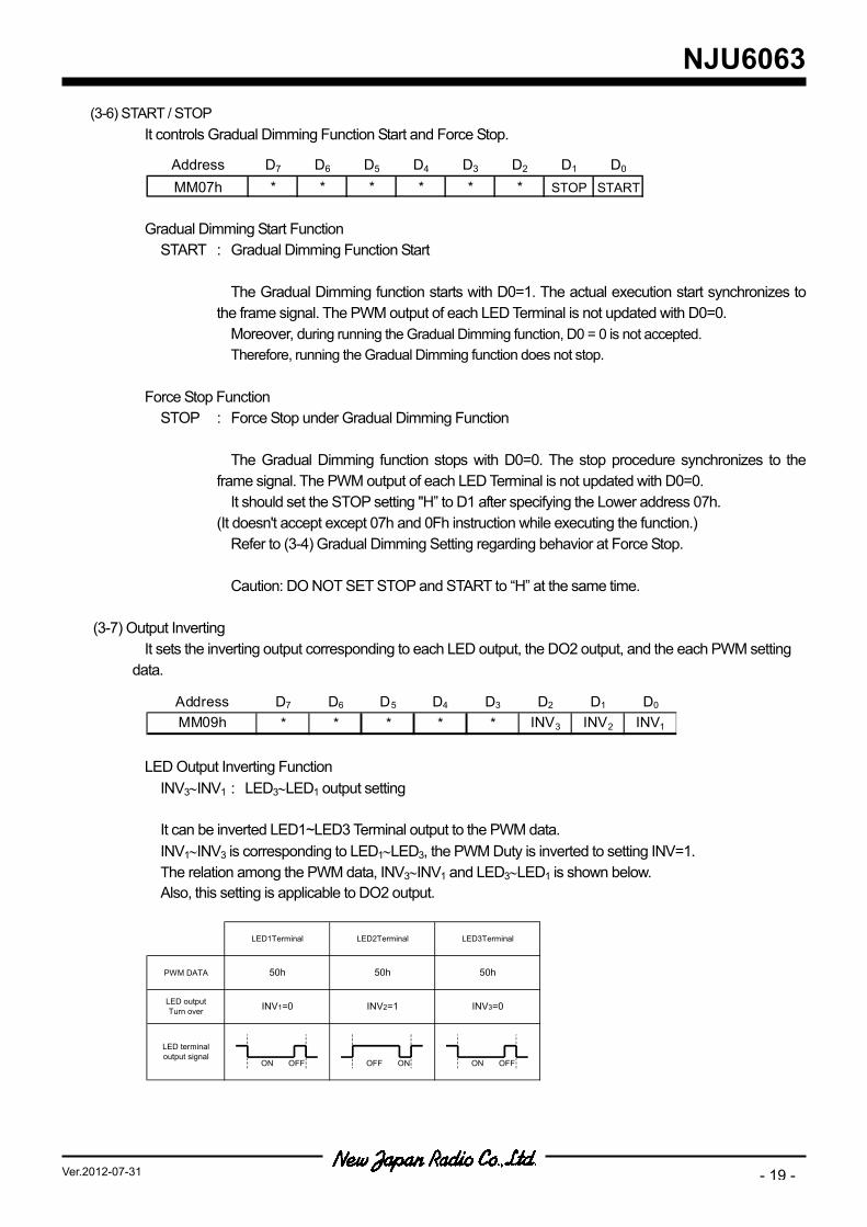
(3-6) START / STOP It controls Gradual Dimming Function Start and Force Stop.
Gradual Dimming Start Function START : Gradual Dimming Function Start The Gradual Dimming function starts with D0=1. The actual execution start synchronizes to the frame signal. The PWM output of each LED Terminal is not updated with D0=0. Moreover, during running the Gradual Dimming function, D0 = 0 is not accepted. Therefore, running the Gradual Dimming function does not stop. Force Stop Function STOP : Force Stop under Gradual Dimming Function The Gradual Dimming function stops with D0=0. The stop procedure synchronizes to the frame signal. The PWM output of each LED Terminal is not updated with D0=0. It should set the STOP setting "H” to D1 after specifying the Lower address 07h. (It doesn't accept except 07h and 0Fh instruction while executing the function.) Refer to (3-4) Gradual Dimming Setting regarding behavior at Force Stop. Caution: DO NOT SET STOP and START to “H” at the same time. (3-7) Output Inverting It sets the inverting output corresponding to each LED output, the DO2 output, and the each PWM setting data.
LED Output Inverting Function INV3∼INV1 : LED3∼LED1 output setting It can be inverted LED1~LED3 Terminal output to the PWM data. INV1∼INV3 is corresponding to LED1∼LED3, the PWM Duty is inverted to setting INV=1. The relation among the PWM data, INV3∼INV1 and LED3∼LED1 is shown below. Also, this setting is applicable to DO2 output.
Address D7 D6 D5 D4 D3 D2 D1 D0
MM07h * * * * * * STOP START
PWM DATA
ON OFF OFF ON ON OFF
LED terminaloutput signal
LED1Terminal LED2Terminal LED3Terminal
LED outputTurn over
50h 50h 50h
INV1=0 INV2=1 INV3=0
D7 D6 D5 D4 D3 D2 D1 D0
* * * * * INV3 INV2 INV1
AddressMM09h

NJU6063
- 20 - Ver.2012-07-31
(3-8) Gradual dimming check It can be confirmed whether gradual dimming function is operated by writing arbitrary data to address 0Bh.
The written data doesn't influence operation. ACK is output while Gradual Dimming is operating. When Gradual Dimming doesn't operate, ACK is not output. Whether all devices Gradual Dimming operating that connects the Multi Device is completed can be confirmed by using this function. By using this function, it can check the Gradual Dimming operation completion of all multi-device connected devices. When data is written at address FF0Bh, ACK is not output if Gradual Dimming operation of all devices is completed. If one or more devices are working, ACK is output. (3-9) Multi device address set It sets upper address to use Multi Device connection.
There is upper address (MA) from 01h to FEh, and it can be set 254 different addresses. When FF0Xh is set, the register of all connected devices is rewritten at the same time. (3-10) Test mode DO NOT USE this mode. This is instruction for IC chip test.
Address D7 D6 D5 D4 D3 D2 D1 D0
MM0Dh MA7 MA6 MA5 MA4 MA3 MA2 MA1 MA0
Address D7 D6 D5 D4 D3 D2 D1 D0
MM0Bh * * * * * * * *

NJU6063
- 21 -Ver.2012-07-31
(4) Memory map MMMM_MMMM : Multi device address. 8 bit 0000_0001(1) to 1111_1110(254) control resistor
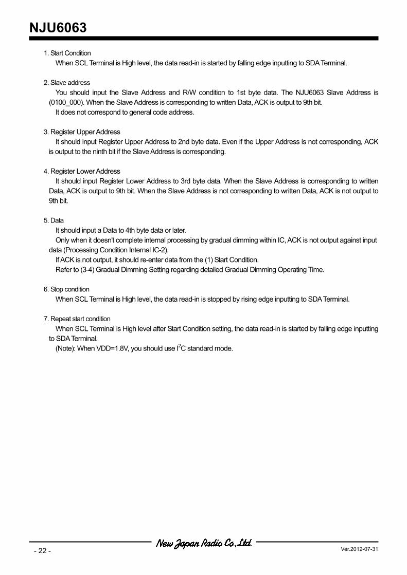
(5) Data input timing The Data format is shown below. There are the Upper Address and the Lower Address with the Slave Address. When multi Device control is used, the Upper address is used for the device select. The Lower address identifies each instruction. You should set 00h when you do not use the Multi Device Control (For 1 piece use). The data of SDA is retrieved by rising edge about SCL. The Lower Address does the increment based on the Lower Address increment set (AI) instruction. It is possible to write it continuously until the stop condition is approved.
S:START Condition
A:ACK
P:STOP Condition
1 2 7 8 9 1 2 7 8 9 1 2 7 8 9
Upper Address Lower Address
SCL
SDA
LSB W
Input DataS PSlave Address R/W A A A
MSB LSB MSB LSB
A
1 2 7 8 9
LSBMSBMSB
Processing Condition Internal IC 2
Processing Condition Internal IC 1
ACK Signal
Gradual dimming mode Wait Data
Wait DataGradual dimming mode
ACK Signal
M M M M _ M M M M 0 0 0 0 _ 0 0 0 0 Initial Setting
M M M M _ M M M M 0 0 0 0 _ 0 0 0 1 Setting of LED current
M M M M _ M M M M 0 0 0 0 _ 0 0 1 0 LED 1 terminal PWM data
M M M M _ M M M M 0 0 0 0 _ 0 0 1 1 LED 2 terminal PWM data
M M M M _ M M M M 0 0 0 0 _ 0 1 0 0 LED 3 terminal PWM data
M M M M _ M M M M 0 0 0 0 _ 0 1 0 1 Setting of gradual dimming
M M M M _ M M M M 0 0 0 0 _ 0 1 1 0 Static ON
M M M M _ M M M M 0 0 0 0 _ 0 1 1 1 START / STOP
M M M M _ M M M M 0 0 0 0 _ 1 0 0 0 NOP
M M M M _ M M M M 0 0 0 0 _ 1 0 0 1 Output turn over
M M M M _ M M M M 0 0 0 0 _ 1 0 1 0 NOP
M M M M _ M M M M 0 0 0 0 _ 1 0 1 1 Gradual dimming check
M M M M _ M M M M 0 0 0 0 _ 1 1 0 0 NOP
M M M M _ M M M M 0 0 0 0 _ 1 1 0 1 Multi device address
M M M M _ M M M M 0 0 0 0 _ 1 1 1 0 NOP
M M M M _ M M M M 0 0 0 0 _ 1 1 1 1 TEST
1 1 1 1 _ 1 1 1 1 * * * * _ * * * * Global address
RegisterAddress
Upper Address Lower Address
NJU6063
- 22 - Ver.2012-07-31
1. Start Condition When SCL Terminal is High level, the data read-in is started by falling edge inputting to SDA Terminal. 2. Slave address You should input the Slave Address and R/W condition to 1st byte data. The NJU6063 Slave Address is (0100_000). When the Slave Address is corresponding to written Data, ACK is output to 9th bit. It does not correspond to general code address. 3. Register Upper Address It should input Register Upper Address to 2nd byte data. Even if the Upper Address is not corresponding, ACK is output to the ninth bit if the Slave Address is corresponding. 4. Register Lower Address It should input Register Lower Address to 3rd byte data. When the Slave Address is corresponding to written Data, ACK is output to 9th bit. When the Slave Address is not corresponding to written Data, ACK is not output to 9th bit. 5. Data It should input a Data to 4th byte data or later. Only when it doesn't complete internal processing by gradual dimming within IC, ACK is not output against input data (Processing Condition Internal IC-2). If ACK is not output, it should re-enter data from the (1) Start Condition. Refer to (3-4) Gradual Dimming Setting regarding detailed Gradual Dimming Operating Time. 6. Stop condition When SCL Terminal is High level, the data read-in is stopped by rising edge inputting to SDA Terminal. 7. Repeat start condition When SCL Terminal is High level after Start Condition setting, the data read-in is started by falling edge inputting to SDA Terminal. (Note): When VDD=1.8V, you should use I2C standard mode.

NJU6063
- 23 -Ver.2012-07-31
(6) RESET (6-1) Hardware RESET The device is initialized by inputting a “L” into the RSTb terminal. Reset status using the RSTb terminal (A) Oscillation / constant current driver “OFF” (B) Internal Oscillator use (C) Stop of gradual dimming (D) Set of PWM data (LED1 to 3) : 00h (E) Set of frame oscillation : fosc / 2 * 1 * 128 (F) Set of DO1 output mode DM : 00h (output of multi device control signal) (G) Set of DO1 output data DO : 00h (H) Set of current power (ILED0 to ILED5) : 00h ( output is disable ) ( I ) Set of gradual dimming step (STP3, STP2, STP1) : 00h (J ) Set of gradual dimming loop (LOOP4 to LOOP1) : 00h (K) Set of static ON (SON3, SON2, SON2) : 00h (L) Set of turn over PWM data (INV3, INV2, INV1) : 00h (M) Set of multi device address : 00h (N) I2C interface reset (6-2) Power ON RESET NJU6063 is including power ON RESET circuit. The device is initialized by power ON. Operation follows hardware reset.
NJU6063
- 24 - Ver.2012-07-31
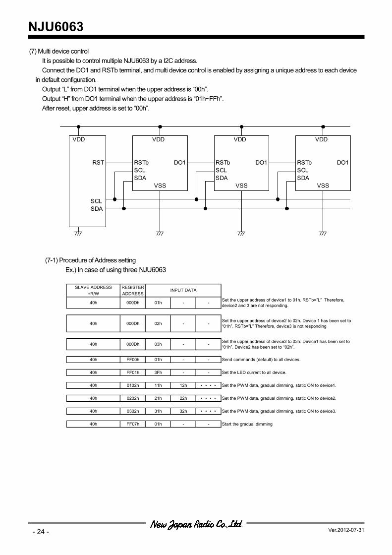
(7) Multi device control It is possible to control multiple NJU6063 by a I2C address. Connect the DO1 and RSTb terminal, and multi device control is enabled by assigning a unique address to each device in default configuration. Output “L” from DO1 terminal when the upper address is “00h”. Output “H” from DO1 terminal when the upper address is “01h~FFh”. After reset, upper address is set to “00h”. (7-1) Procedure of Address setting Ex.) In case of using three NJU6063
VDD
RSTb DO1SCLSDA VSS
VDD
RSTb DO1SCLSDA VSS
VDD
RSTb DO1SCLSDA VSS
VDD
RST
SCL SDA
SLAVE ADDRESS REGISTER+R/W ADDRESS
40h 000Dh 01h - - Set the upper address of device1 to 01h. RSTb=”L” Therefore,device2 and 3 are not responding.
40h 000Dh 02h - - Set the upper address of device2 to 02h. Device 1 has been set to“01h”. RSTb=”L” Therefore, device3 is not responding
40h 000Dh 03h - - Set the upper address of device3 to 03h. Device1 has been set to“01h”. Device2 has been set to “02h”.
40h FF00h 01h - - Send commands (default) to all devices.
40h FF01h 3Fh - - Set the LED current to all device.
40h 0102h 11h 12h ・・・・ Set the PWM data, gradual dimming, static ON to device1.
40h 0202h 21h 22h ・・・・ Set the PWM data, gradual dimming, static ON to device2.
40h 0302h 31h 32h ・・・・ Set the PWM data, gradual dimming, static ON to device3.
40h FF07h 01h - - Start the gradual dimming
INPUT DATA

NJU6063
- 25 -Ver.2012-07-31
• After reset upper address Initial value : 00h
• After address set Initialization
(8) Control of NJU6080 NJU6080 can be controlled by using the terminal DO1 and the terminal DO2 of NJU6063. (Refer to APPRICATION CIRCUIT Example 2) The LED current can be increased by connecting NJU6080 more than NJU6063. The PWM data of LED3 becomes the PWM data of NJU6080. (8-1) Procedure of NJU6080 control Ex.) In case of lighting with 70/128duty
H L L
VDD
RSTb DO1SCLSDA VSS
VDD
RSTb DO1SCLSDA VSS
VDD
RSTb DO1SCLSDA VSS
VDD
RST
SCL SDA
00h 00h 00h
H
VDD
RSTb DO1SCLSDA VSS
VDD
RSTb DO1SCLSDA VSS
VDD
RSTb DO1SCLSDA VSS
VDD
RST
SCL SDA
01h 02h 03hH H
SLAVE ADDRESS REGISTER+R/W ADDRESS
40h 0000h C1h - -Send of Function set."H" is output from the terminal DO1 by setting DM=1 and DO=1.NJU6080 is enable.
40h 0001h 0Fh - - Set of LED3 current to 0 LED3.OFF state of LED3
40h 0004h 46h 48h ・・・・ Set the PWM data, gradual dimming, static ON to LED3.
40h 0007h 01h - - The gradual dimming operation begins by START/STOP.(NJU6080 lights with 70/128Duty )
INPUT DATA
NJU6063
- 26 - Ver.2012-07-31
APPLICATION CIRCUIT < Example 1 >
< Example 2 (Connect NJU6080) >
CPU
LED1
LED2
LED3
AVSS
NJU6063SDA
SCL
RSTb
DO2
DO1
OSC
VDD
VSS ISET
VIN
3V
3.3kΩ
10kΩ10kΩ
5V
NJU6080
CPU
LED1
LED2
LED3
AVSS
NJU6063SDA
SCL
RSTb
DO2
DO1
OSC
VDD
VSS ISET
VIN
RSGND
VDD
LEDEN
PWM
10kΩ10kΩ
3.3kΩ
2Ω
3V 5V
NJU6063
- 27 -Ver.2012-07-31
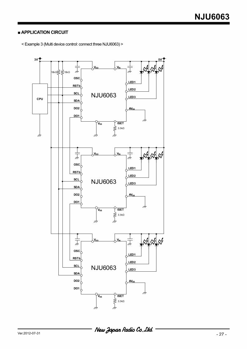
APPLICATION CIRCUIT < Example 3 (Multi device control: connect three NJU6063) >
CPU
3.3kΩ
LED1
LED2
LED3
AVSS
NJU6063SDA
SCL
RSTb
DO2
DO1
OSC
VDD
VSS ISET
VIN
LED1
LED2
LED3
AVSS
NJU6063SDA
SCL
RSTb
DO2
DO1
OSC
VDD
VSS ISET
VIN
LED1
LED2
LED3
AVSS
NJU6063SDA
SCL
RSTb
DO2
DO1
OSC
VDD
VSS ISET
VIN
3V
10kΩ10kΩ
3.3kΩ
3.3kΩ
5V
NJU6063
- 28 - Ver.2012-07-31
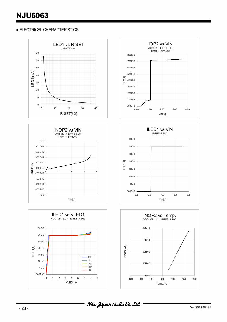
ELECTRICAL CHARACTERISTICS
ILED1 vs RISETVIN=VDD=3V
0
10
20
30
40
50
60
70
0 10 20 30 40
RISET[kΩ]
ILE
D1[
mA
]
IOP2 vs VINVDD=3V, RISET=3.3kΩ
LED1~LED3=2V
000E+0
100E-6
200E-6
300E-6
400E-6
500E-6
600E-6
700E-6
800E-6
0.00 2.00 4.00 6.00 8.00
VIN[V]
IOP2
[A]
INOP2 vs VINVDD=3V, RISET=3.3kΩ
LED1~LED3=2V
-1E-9
-800E-12
-600E-12
-400E-12
-200E-12
000E+0
200E-12
400E-12
600E-12
800E-12
1E-9
0 2 4 6 8
VIN[V]
INO
P2[A
]
ILED1 vs VINRISET=3.3kΩ
000E+0
5E-3
10E-3
15E-3
20E-3
25E-3
30E-3
35E-3
0.0 2.0 4.0 6.0 8.0
VIN[V]
ILED
1[A]
ILED1 vs VLED1VDD=VIN=3.0V , RISET=3.3kΩ
000E+0
5E-3
10E-3
15E-3
20E-3
25E-3
30E-3
35E-3
0 1 2 3 4 5 6 7 8
VLED1[V]
ILED
1[A]
-502575125150
INOP2 vs Temp.VDD=VIN=3V , RISET=3.3kΩ
1E+0
10E+0
100E+0
1E+3
10E+3
-100 -50 0 50 100 150 200
Temp.[ºC]
INO
P2[
nA]

NJU6063
- 29 -Ver.2012-07-31
ELECTRICAL CHARACTERISTICS
fOSC vs Temp.VDD=VIN=3V
800
850
900
950
1000
1050
1100
1150
1200
-100 -50 0 50 100 150 200
Temp.[ºC]
fOSC
[kH
z]
ILED_OFFH1 vs Temp.VDD=VIN=3V , RISET=3.3kΩ, VI=5.5V
10E-3
100E-3
1E+0
10E+0
100E+0
1E+3
10E+3
-100 -50 0 50 100 150 200
Temp.[ºC]
ILED
_OFF
H1[
nA]

NJU6063
- 30 - Ver.2012-07-31
[CAUTION] The specifications on this data book are only
given for information , without any guarantee as regards either mistakes or omissions. The application circuits in this data book are described only to show representative usages of the product and not intended for the guarantee or permission of any right including the industrial rights.