
RF Wireless Text Messaging System - Harvey Mudd...
41
RF Wireless Text Messaging System Final Project Report December 8, 2000 E155 Braden Pellett and Steve Yan Abstract: One of the hot topics in modern computing is wireless communication. WAP and Bluetooth technologies are poised to revolutionize the way that electronic devices and the humans who use them will interact in the future. In the spirit of such up and coming technology, the objective of this project is to design and implement a wireless communication system using RF wireless transceivers. The system incorporates a multi-layered communication protocol with packet recognition and simple handshaking. Each transceiver station consists of a 4x4 matrix keypad for input, LCD for text display, half-duplex transceiver, FPGA board, and M68HC11EVB. On user input or incoming data, the FPGA alerts the HC11 via external interrupt signals. The HC11 controls an LCD display menu system and writes data to memory. The menu system allows the user to input a message for transmission or to view the past six received messages.
Transcript of RF Wireless Text Messaging System - Harvey Mudd...

RF Wireless Text Messaging System
Final Project Report December 8, 2000
E155
Braden Pellett and Steve Yan Abstract: One of the hot topics in modern computing is wireless communication. WAP and Bluetooth technologies are poised to revolutionize the way that electronic devices and the humans who use them will interact in the future. In the spirit of such up and coming technology, the objective of this project is to design and implement a wireless communication system using RF wireless transceivers. The system incorporates a multi-layered communication protocol with packet recognition and simple handshaking. Each transceiver station consists of a 4x4 matrix keypad for input, LCD for text display, half-duplex transceiver, FPGA board, and M68HC11EVB. On user input or incoming data, the FPGA alerts the HC11 via external interrupt signals. The HC11 controls an LCD display menu system and writes data to memory. The menu system allows the user to input a message for transmission or to view the past six received messages.
2
I. Introduction
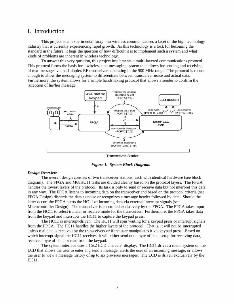
This project is an experimental foray into wireless communication, a facet of the high technology industry that is currently experiencing rapid growth. As this technology is a lock for becoming the standard in the future, it begs the question of how difficult it is to implement such a system and what kinds of problems are inherent in wireless technology. To answer this very question, this project implements a multi-layered communications protocol. This protocol forms the basis for a wireless text messaging system that allows for sending and receiving of text messages via half-duplex RF transceivers operating in the 900 MHz range. The protocol is robust enough to allow the messaging system to differentiate between transceiver noise and actual data. Furthermore, the system allows for a simple handshaking protocol that allows a sender to confirm the reception of his/her message. Design Overview The overall design consists of two transceiver stations, each with identical hardware (see block diagram). The FPGA and M68HC11 tasks are divided cleanly based on the protocol layers. The FPGA handles the lowest layers of the protocol. Its task is only to send or receive data but not interpret this data in any way. The FPGA listens to incoming data on the transceiver and based on the protocol criteria (see FPGA Design) discards the data as noise or recognizes a message header followed by data. Should the latter occur, the FPGA alerts the HC11 of incoming data via external interrupt signals (see Microcontroller Design). The transceiver is controlled exclusively by the FPGA. The FPGA takes input from the HC11 to select transfer or receive mode for the transceiver. Furthermore, the FPGA takes data from the keypad and interrupts the HC11 to capture the keypad press. The HC11 is interrupt-driven. The HC11 will spin waiting for a keypad press or interrupt signals from the FPGA. The HC11 handles the higher layers of the protocol. That is, it will not be interrupted unless real data is received by the transceivers or if the user manipulates it via keypad press. Based on which interrupt signal the HC11 receives, it will either send out a byte of data, setup for receiving data, receive a byte of data, or read from the keypad. The system interface uses a 16x2 LCD character display. The HC11 drives a menu system on the LCD that allows the user to enter and send a message, alerts the user of an incoming message, or allows the user to view a message history of up to six previous messages. The LCD is driven exclusively by the HC11.
FPGA M68HC11EVB
Transceiver Station
RF
transceiver
LCD module
3
4x4 matrixkeypad
8
8 3
2
4
keypad data port(PORTE [7:0])
8
transceiver data port(PORTC [7:0])
8
LCD data(PORT B [7:0])
LCD control(PORTA [5:3])
txen, rxen,txdata
rxdata
external interrupts(PORTA [2:0], STRA)
transceiver enable,direction select(PORTA [7:6])
Figure 1. System Block Diagram.
3
II. New Hardware This text messaging system uses two new types of hardware: an LM016 16x2 LCD character display and a Linx Technologies SC-PA Series RF transceiver module. LM016 16x2 LCD Character Display (LM016) This LCD includes an on-board driver that handles functionality such as recognizing characters, writing characters to the display, and moving the cursor. Therefore using the LCD is simply a matter of issuing the correct series of commands to the LCD. This LCD display is controlled via 14 pins (see Schematics). The first three pins (GND, Vcc, Ve) control power to the LCD. An external potentiometer is tied to these three pins to control the intensity of the LCD display.
The next three pins (RS, R/W, E) are used as control pins. Writing to these pins and then issuing specific commands to the data pins will cause different functionality on the LCD. Pin 4 (Register Select) should be high when writing characters to the display and low when writing to control registers. Pin 5 (Read/Write) allows a user to either write data to the display or read from its on-board memory. The read functionality was not used in this project. Pin 6 (Enable) should be strobed low after setting up the data pins. The data on pins 7-14 are latched on the falling edge of this signal.
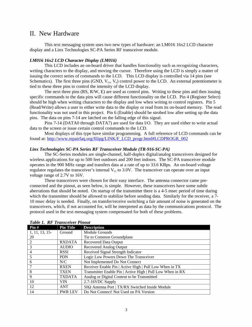
Pins 7-14 (DATA0 through DATA7) are used for data I/O. They are used either to write actual data to the screen or issue certain control commands to the LCD. Most displays of this type have similar programming. A full reference of LCD commands can be found at: http://www.repairfaq.org/filipg/LINK/F_LCD_progr.html#LCDPROGR_002 Linx Technologies SC-PA Series RF Transceiver Module (TR-916-SC-PA) The SC-Series modules are single-channel, half-duplex digital/analog transceivers designed for wireless applications for up to 500 feet outdoors and 200 feet indoors. The SC-PA transceiver module operates in the 900 MHz range and transfers data at a rate of up to 33.6 KBps. An on-board voltage regulator regulates the transceiver’s internal Vcc to 3.0V. The transceiver can operate over an input voltage range of 2.7V to 16V. These transceivers were chosen for their easy interface. The antenna connector came pre-connected and the pinout, as seen below, is simple. However, these transceivers have some subtle aberrations that should be noted. On startup of the transmitter there is a 4-5 msec period of time during which the transmitter should be allowed to stabilize before sending data. Similarly for the receiver, a 7-10 msec delay is needed. Finally, on transfer/receive switching a fair amount of noise is generated on the transceivers, which, if not accounted for, will be interpreted as data by the communications protocol. The protocol used in the text messaging system compensated for both of these problems. Table 1. RF Transceiver Pinout Pin # Pin Title Description 1, 11, 13, 15-20
Ground Module Grounds Tie to Common Groundplane
2 RXDATA Recovered Data Output 3 AUDIO Recovered Analog Output 4 RSSI Received Signal Strength Indicator 5 PDN Logic Low Powers Down The Transceiver 6 N/C Not Implemented Do Not Connect 7 RXEN Receiver Enable Pin | Active High | Pull Low When in TX 8 TXEN Transmitter Enable Pin | Active High | Pull Low When in RX 9 TXDATA Analog or Digital Content to be Transmitted 10 VIN 2.7-16VDC Supply 12 ANT 50Ω Antenna Port | TX/RX Switched Inside Module 14 PWR LEV Do Not Connect! Not Used on PA Version

4
III. Schematics
1 GND2 RX DATA3 AUDIO4 RSSI5 PDN6 N/C7 RXEN8 TXEN9 TXDATA10 VIN
GND 20GND 19GND 18GND 17GND 16GND 15
PWRLEV 1413
ANT 1211+5VDC
FP8FP9
FP18
Transceiver
Matrix Keypad
COL3COL2COL1COL0
ROW0ROW1ROW2ROW3
P28P29P35P36P38P39P40P44
1K 1K 1K 1K
+5VDC
+5VDC
FP23 (red LED)
FP24 (yellow LED)
FP25 (green LED)
DATA7 L14DATA6 L13DATA5 L12DATA4 L11DATA3 L10DATA2 L9DATA1 L8DATA0 L7 E L6R/W L5RS L4
Ve
L3 Vcc
L2
GND
L1
H35 (PB7)H36 (PB6)H37 (PB5)H38 (PB4)H39 (PB3)H40 (PB2)H41 (PB1)H42 (PB0)H30 (PA4)H29 (PA5)H28 (PA6)
+5VDC
LCD Display Module
+5VDC
47K
P19
Reset switch
L = LCD DisplayF = FPGA BoardH = M68HC11
FP84FP83FP82FP81FP80FP79FP78FP77FP72
FP70/LED1FP69/LED2FP68/LED3FP67/LED4FP66/LED5FP65/LED6FP62/LED7FP61/LED8
FP59FP58FP57FP56FP45
(PC0)(PC1)(PC2)(PC3)(PC4)(PC5)(PC6)(PC7)(PA0)(PE0)(PE1)(PE2)(PE3)(PE4)(PE5)(PE6)(PE7)H4 (STRA)(PA1)(PA6)(PA7)(PA2)
FPGA/HC11 Interface

5
IV. Microcontroller Design
The M68HC11 handles controlling the LCD-displayed menu system, storing received messages, and allowing for input and transmission of a text message. All 68HC11 functionality is either polling or interrupt-driven. Table 2 shows the various input and output signals accepted and generated by the HC11: Table 2. Microcontroller I/O Inputs Outputs Transceiver Data Port (PORTC) Keypad Data Port (PORTE) Receiver Incoming Transmission IRQ (PA2) Receiver Data Ready IRQ (STRA) Transmitter Data Request IRQ (PA1) Keypad Data Ready (Polling) (PA0)
Transceiver Data Port (PORTC) Transceiver Direction Select (PA7) Transmitter Enable (PA6) LCD Data (PORTB) LCD Control (PORTA [5:3])
Program Data The HC11 tracks a wide variety of program data to help it decide which subroutines to execute based on incoming interrupt or polling signals. Most notably it remembers which screen is displayed on the LCD, where in memory data to be transmitted is stored, and where in memory previous messages have been stored (see Appendix B for a full listing of program data). Data Structure The messages sent and received by each transceiver station expect the following structure for each message:
1. Control character. This first byte denotes if the message is an actual text message or simply a handshake.
2. Data. If there is text to be sent, the words of the message (up to 32 characters) immediately follow the message control character. If this is simply a handshake, no data is sent after the control character.
Handshaking The HC11 controls a simple handshaking protocol that will allow a user to verify if the other transceiver station correctly received his/her message. If a transceiver station receives what it identifies as a valid message, it will immediately send out a handshake signal to alert the sender that a message was received. The sender will then display on the LCD that the transmission was successful. If no such handshaking signal is received after a certain timeout period (1 msec in this case) then the sending station displays a failure message. Transfer/Receive Switching The HC11 will be able to send and receive messages by controlling the physical RF transceiver module via the FPGA. It uses two output signals to accomplish this: Transmitter Enable and Direction Select. When Direction Select is low, the transceiver is set to transmit. When Direction Select is high, the transceiver is set to receive. When Transmitter Enable is high, this prompts the FPGA to repeatedly fire the Transmitter Data Request Interrupt in order to send a message byte by byte from the HC11. When sending data, the HC11 cannot switch back to receive mode immediately after sending the stop byte. Although the HC11 will be finished sending, the FPGA will still be piping data serially to the RF transceiver. Switching during this period will prematurely terminate the outgoing data. Conversely, the HC11 should not be allowed to switch to transfer mode until any incoming messages have been completely sent.

6
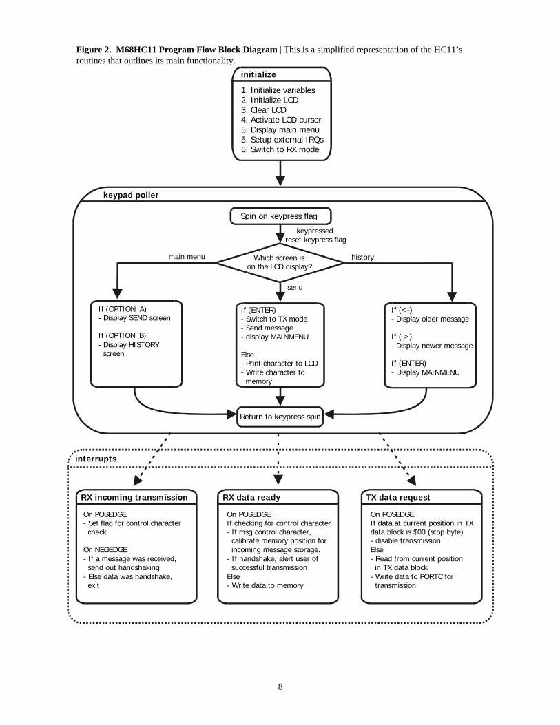
To fix this problem, the HC11 monitors different input and output signals to determine when it is safe to switch from receive to transfer and vice-versa. It cannot enter transfer mode until the Receiver Incoming Transmission Interrupt signal is low. This guarantees that switching will not cut off any incoming data. Furthermore, the HC11 cannot enter receive mode until the Transmit Enable signal and Transmitter Data Request Interrupt signals are low. When the latter is low, this signifies that the FPGA has completely sent out the byte of data that it last read from PORTC. Polling and Interrupts Figure 2 shows a simplified version of the microcontroller’s program flow. Note that the HC11 will only execute its subroutines if either a) a keypress is detected or b) an interrupt signal goes high. In this sense the HC11 is usually slave to the FPGA except on initializing data transmission, where it will raise the transfer enable signal to prompt the FPGA to pull data from the HC11 on the Transceiver Data Port (PORTC). The keypress poller spins on the Keypad Data Ready flag (IC3F). When a key is pressed on the matrix keypad and the FPGA raises this signal, the poller will break from its spin and traverse the rather lengthy if-then-else keypress logic. The HC11 will call different subroutines based on which screen (main menu, send screen, or view history) is currently on the LCD and which keys on the keypad are pressed. The keypress poller was originally made an interrupt, however due to its length and non-time critical nature, it was downgraded to a polling scheme in order to eliminate the risk of this lengthy routine from delaying other more time-critical interrupts. At any point during the keypress polling routine, an external interrupt signal from the FPGA can trigger one of three interrupt service routines (ISR) to fire. These three interrupt signals are: Receiver Incoming Transmission, Receiver Data Ready, and Transmitter Data Request. Each of these signals prompts the HC11 to setup for incoming messages, send a data word, or receive a data word. Receiver Incoming Transmission IRQ
This interrupt alerts the HC11 that the FPGA has recognized a valid data packet and that incoming data is imminent. This signal will stay high for the duration of the message reception. To prepare for this data, on this interrupt’s positive edge the ISR for Receiver Incoming Transmission raises a flag that instructs the Receive Data Ready ISR to look for one of the two control characters corresponding to either an incoming message or a handshake confirmation.
This ISR will also trigger on the negative edge of the interrupt signal. If a handshake was just received, the ISR need not do anything since this is simply confirmation that the last message it sent out was properly received. If a message was just received however, the HC11 will nest Transmitter Data Request interrupts within this ISR in order to send out a handshaking response immediately. Receiver Data Ready IRQ The Receiver Data Ready signal fires every time the FPGA reads in a new byte of incoming data. When this signal is raised, the ISR will do different things based upon the flags that are set within the program. If the “Expect Control Character” flag is raised, then the ISR attempts to interpret the byte of data that it reads from PORTC as one of the two control characters. If neither can be matched to the data, the ISR immediately disregards the entire message. If the data is a message, then the ISR will calibrate a new position in the history memory block and subsequently treat each successive byte as a byte of an incoming message, storing it to memory. If the data is a handshake, the ISR disregards any other data following the handshake control character. This is merely confirmation that the other transceiver station received the previously sent message. When the Receiver Incoming Transmission Interrupt goes low, this signifies the end of an incoming message. A stop byte ($00) is used to terminate the string written to memory.

7
Transmitter Data Request IRQ The Transmitter Data Request signal fires every time the FPGA requests a new piece of data from the HC11. This signal will only fire if the Transmitter Enable signal is high. The ISR reads a byte of data from the block of memory that records the message to be transmitted and writes this data to PORTC for output. When the ISR sees the stop byte ($00), this signifies that the message is finished and the ISR sets the Transmission Enable signal low. The ISR does not send the stop byte. Message History The text messaging system message history is a circular array of six 33-byte blocks of memory. This circular setup eliminates the need to shift all the previous messages over in memory when the history has been filled and a new message has come in. Rather, before a new message comes in the HC11 calculates from the address of the current newest message where the address of the next new message will be. Should it hit the limit of the memory block devoted to message history, it will wrap to the front of the history memory block to store the new message. LCD Display and Control Writing to the LCD display is controlled via PORTB and three bits of PORTA. A series of LCD control subroutines along with subroutines that draw specific screen types (main menu, send screen, view history) are used to represent to the user the changing state of the text messaging system. The LCD display will change in response to different keypresses in different areas of the menu system. Since the LCD display requires a delay on the order of 3-5 msec between writing characters, LCD display writing subroutines are called from the main program rather than from interrupt service routines to minimize interrupt delays.
8
initialize
1. Initialize variables2. Initialize LCD3. Clear LCD4. Activate LCD cursor5. Display main menu5. Setup external IRQs6. Switch to RX mode
keypad poller
Spin on keypress flag
keypressed.reset keypress flag
main menu history
send
Which screen ison the LCD display?
If (ENTER)- Switch to TX mode- Send message- display MAINMENU
Else- Print character to LCD- Write character to memory
If (OPTION_A)- Display SEND screen
If (OPTION_B)- Display HISTORY screen
On POSEDGE- Set flag for control character check
On NEGEDGE- If a message was received, send out handshaking- Else data was handshake, exit
On POSEDGEIf checking for control character- If msg control character, calibrate memory position for incoming message storage.- If handshake, alert user of successful transmissionElse - Write data to memory
On POSEDGEIf data at current position in TXdata block is $00 (stop byte)- disable transmissionElse- Read from current position in TX data block- Write data to PORTC for transmission
If (<-)- Display older message
If (->)- Display newer message
If (ENTER)- Display MAINMENU
Return to keypress spin
interrupts
RX incoming transmission RX data ready TX data request
Figure 2. M68HC11 Program Flow Block Diagram | This is a simplified representation of the HC11’s routines that outlines its main functionality.
9
V. FPGA Design
The FPGA holds three main components: the keypad decoder, the RF serial data transmitter, and the RF serial data receiver. All the components use two primary signals: the input clock (clk) and the global reset (reset_L).
Keypad
The keypad decoder module polls a 4x4 matrix keypad for input (polling on keypad_cols and watching for input on keypad_rows). It outputs the typed value using an ASCII encoded word on an 8-bit bus (keypad_data_port), and uses the positive edge of another signal (keypad_data_ready) to indicate new data is available. As part of the keypad decoding, three keys in the right most column are designated as shift keys, which change which characters are decoded for the first three columns. There is also 3 outputs which indicate which shift key, if any, is active (shift_L[0..2]). Refer to appendix C for the keypad layout.
RF Serial Data Transceiver Design Description
The other two main components on the FPGA, the RF serial data transmitter and the RF serial data receiver, handle the lower layers of the designed communication protocol, while the upper layers are on the 68HC11 microcontroller. What this means is that the FPGA handles all aspects of the communication of individual words of data, but does not interpret the meaning of the words in any way. The microcontroller handles the meaning of individual words, but is not concerned with how these words are communicated. The rest of this section is concerned with the operation of the communication modules in the FPGA. Refer to the microcontroller section for an explanation of the higher-lever protocol. In figuring out how to send data words over the RF wireless link using the receiver modules, a few facts needed to be considered. First, the transceiver makes no assumptions about the serial data, and does not encode it in any way. Secondly, the transceiver module needs to have a square wave that alternates enough so that its data slicer has some frequency on which to lock. Finally, there is the definite possibility for noise, which the protocol should handle with some grace. In addressing these issues, communication of data words with the FPGA is split up into a header and the data. In turn, the header is split up into a wake-up preamble and a data word alignment region. The data section is just a stream of, currently, 8-bit data words. All transmissions have a carrier frequency which dictate the maximum frequency at which the serial transmission alternates, and is the rate the transmission tries to stay close to as not to confuse the transceiver module. As of the time of this report, a 15.6 KHz maximum frequency square wave using a 1 MHz main clock into the FPGA was employed. The header consists of a wake-up preamble and a data word alignment region. Before the preamble, the serial data is pulled to a constant high. The wakeup preamble consists of an alternating sequence of 30 “sub-bits” that are transmitted at the base frequency of communication. A “sub-bit” will be defined as a high or low signal lasting half the carrier period. After the wakeup preamble, a special sequence of sub-bits is sent (HHLHHLHLLHLL), followed by 12 more alternating sub-bits. After this, data transmission begins. Data, it should be noted, is encoded using a set of three sub-bits, where a 1 is HHL and 0 is HLL. The wake-up preamble has three purposes: to setup the data-slicer in the transceiver module, to establish a phase lock between the transmitting and receiving clocks, and to let the receiver know that a header is beginning. The receiver, in order to establish a phase lock with the transmitting clock, and to try to average out noise pulses, samples each sub-bit 8 times. When waiting for data, the receiver goes through the following steps:

10
Figure 3. Message Header | A series of 32 sub-bits followed by a data word alignment.
1. Compare the sampled serial input to a well-defined positive edge. It will pick up on one of the wake-up preamble’s pulses, and synchronize itself to the edges of this square wave, so it knows the alignment of the sub-bits.
2. To make sure that there is actually a preamble being received (and not, say, a noise burst), it
checks to see if there is a high-low-high-low-high-low (HLHLHL) pattern in the serial data. A “high” or a “low” is determined from the sampled serial input by finding the majority value of the 8 samples.
3. Now the receiver synchronizes to the data words by searching for the HHLHHLHLLHLL
sub-bit sequence. 4. Finally, it waits for 12 more sub-bits before turning over control to the data word extracting
section in order to synchronize itself with the incoming data words. These sub-bits are placed in the serial transmission so that the receiver cannot accidentally mistake where the data word alignment sub-bit sequence really is, since high-low-high-low (HLHL) sub-bit sequences cannot easily appear in encoded data-bit sequences, even with heavy noise.
Steps 2 and 3 have a timeout timer associated with them that will make the receiver give up
looking for the expected input and return to step 1 after a certain number of candidate sub-bits have passed by. This is especially important for step 3. Otherwise the receiver might skip the true 4-bit word (e.g. due to noise) and start looking for it inside the data portion of the transmission, which would cause all data to be incorrectly aligned. See figure 3 for an example of the header.
Now data words being to be decoded. The transmitter, as mentioned earlier, encodes each data-
bit of the word with three sub-bits (1 = HHL, 0 = HLL). This way, the serial output will not remain at a single high or low state for very long, and thus there is a base frequency for the transceiver to pick up on. The data section of the transmission is just a string of bits encoded in the above way. Once data words begin to be recognized, the receiver outputs them to the 8-bit data but. When the receiver gets a word of completely invalid encoded bits (most likely because the serial input has returned to its default constant-high state, which is what the transmitter section will do once it is done sending data), the receiver resets to searching for a transmission header. See figure 4 for an example of the data transmission.

11
Operation Description Since the RF transceivers are half-duplex, only one bi-directional port is used for data input or output (transceiver_data_port). Another signal selects whether the FPGA should be in transmit or receive mode (transceiver_direction_select).
The transmitter module when not communicating just sends out a constant high signal. It uses an enable signal (transmitter_enable) to start communication. It will sample the data input on an 8-bit bus (transceiver_data_port). An output signal (transmitter_data_request) indicates on its positive edge that the transmitter has sampled the input data bus, and so new data may be asserted. When the enable signal is set low again, the transmitter finishes the word it is on, and resets to its initial state. The data request signal goes low after the transmitter has been disabled only when the transmitter has finished sending the last pieces of data and a sufficiently long period of a constant high signal to tell the receiver that the data has ended.
The receiver module waits for a valid incoming transmission. Once it identifies one, it sets a signal telling a transmission is arriving (receiver_incoming_transmission). Then it starts decoding the data words, which are then loaded to an 8-bit bus (transceiver_data_port), and then uses the positive edge of another signal to indicate data is ready on the bus (receiver_data_ready). This decoding continues until the serial data stream stops being valid for an entire data word, at which points the receiver resets to its initial state, and so the incoming transmission signal is also reset.
Figure 4. Message Header followed by data words.

12
VI. Results
All of our tests of the final product returned favorable results. The lower level protocol effectively discarded noise and never was falsely triggered by such noise. Further, when sending data, all the words got through intact if the FPGA successively picked up the incoming signal, which it did almost all the time (at ranges tested up to the distance across the lab). The upper levels of the protocol also behaved as expected, and our handshaking implementation was able to determine if the receiver had picked up the message or not. Outside of the protocol, the other features (mostly made up of user-interfaces) also worked as expected. The keypad and the LCD operated properly. Interface features for the text messaging system program, namely a menu system, a message history, and a automatic indicator of a new message, all worked as designed. The most challenging portion of the design was the protocol in general. In particular, the lower levels presented some interesting challenges to overcome, as discussed in the FPGA section. However, every major portion of the project presented some problem to solve, all of which (no matter how small) helped to further our understanding of the hardware we were working with. Overall, we accomplished the goals set out in our final proposal, and were even able to go a bit further. The experience we received with the technology should prove useful, or at least make good small talk at parties. Hopefully the information contained in this document will adequately inform the reader of the issues and challenges of implementing this or a similar design.

13
References [1] http://www.repairfaq.org/filipg/LINK/F_LCD_progr.html#LCDPROGR_002 [2] http://www.fe.uni-lj.si/~tuma/seminarske/senzor/lm016/znaki.htm [3] "Digital Alarm Clock", Jason Fong, Fernando Mattos
http://www3.hmc.edu/~harris/class/e155/projects99/alarmclock1.pdf [4] http://www.linxtechnologies.com/lpdfs/scpamanual.pdf [5] http://www.linxtechnologies.com/lpdfs/scpadata.pdf
Parts List Listing of all the components used other than standard resistors, capacitors, and parts available in the MicroP’s lab. Part Source Vendor Part # Quantity Price Linx Half-Duplex RF Transceiver RF Digital
http://www.rfdigital.com TR-916-SC-PA 2 $96.60
10 Pin Terminal Strips Mar-Vac Electronics 510AG91F10ES 2 $4.18 40 Pin Header Mar-Vac Electronics - 2 $1.98 Two Row 60 Pin Header Mar-Vac Electronics - 2 $2.98 16x2 LCD Char. Display Stock Room LM016 Breadboard Radio Shack - 2 $9.98 TOTAL: $115.72
14
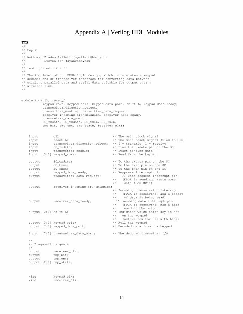
Appendix A | Verilog HDL Modules
TOP // // top.v // // Authors: Braden Pellett ([email protected]) // Steven Yan ([email protected]) // // Last updated: 12-7-00 // // The top level of our FPGA logic design, which incorperates a keypad // decoder and RF transceiver interface for converting data between // straight parallel data and serial data suitable for output over a // wireless link. // module top(clk, reset_L, keypad_rows, keypad_cols, keypad_data_port, shift_L, keypad_data_ready, transceiver_direction_select, transmitter_enable, transmitter_data_request, receiver_incoming_transmission, receiver_data_ready, transceiver_data_port, SC_rxdata, SC_txdata, SC_txen, SC_rxen, tmp_bit, tmp_cnt, tmp_state, receiver_clk); input clk; // The main clock signal input reset_L; // The main reset signal (tied to GSR) input transceiver_direction_select; // 0 = transmit, 1 = receive input SC_rxdata; // From the rxdata pin on the SC input transmitter_enable; // Start sending data input [3:0] keypad_rows; // Read from the keypad output SC_txdata; // To the txdata pin on the SC output SC_txen; // To the txen pin on the SC output SC_rxen; // To the rxen pin on the SC output keypad_data_ready; // Keypress interrupt pin output transmitter_data_request; // Data request interrupt pin // (FPGA is sending, wants more // data from HC11) output receiver_incoming_transmission; // Incoming transmission interrupt // (FPGA is receiving, and a packet // of data is being read) output receiver_data_ready; // Incoming data interrupt pin // (FPGA is receiving, has a data // word on the output) output [2:0] shift_L; // Indicates which shift key is set // on the keypad. // (active low for use with LEDs) output [3:0] keypad_cols; // Poll the keypad output [7:0] keypad_data_port; // Decoded data from the keypad inout [7:0] transceiver_data_port; // The decoded trasceiver I/O // // Diagnostic signals // output receiver_clk; output tmp_bit; output tmp_cnt; output [2:0] tmp_state; wire keypad_clk; wire receiver_clk;
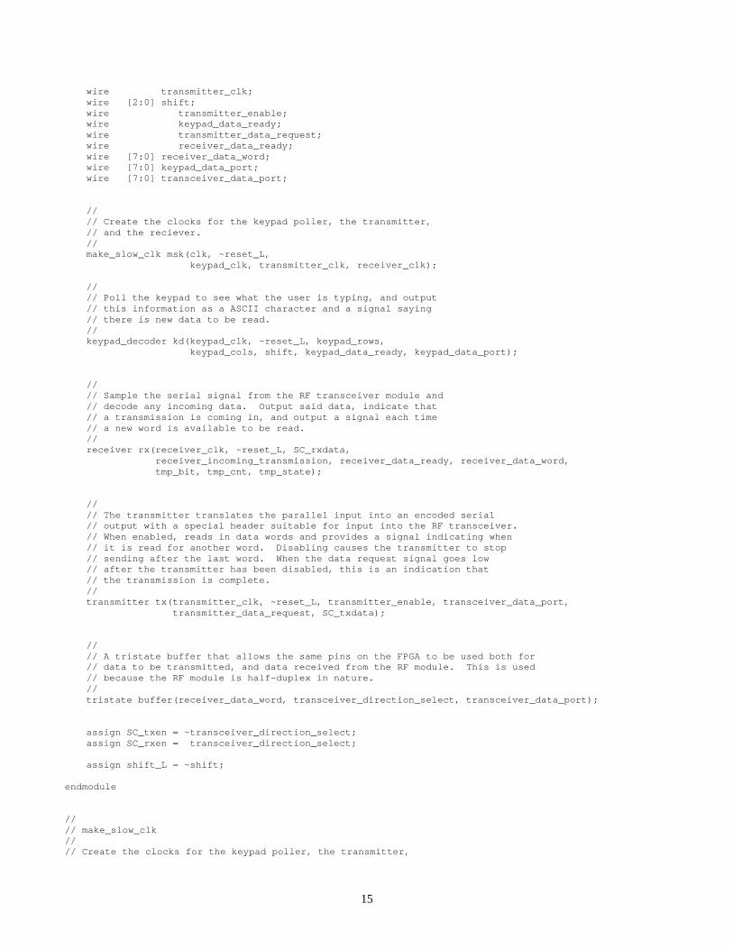
15
wire transmitter_clk; wire [2:0] shift; wire transmitter_enable; wire keypad_data_ready; wire transmitter_data_request; wire receiver_data_ready; wire [7:0] receiver_data_word; wire [7:0] keypad_data_port; wire [7:0] transceiver_data_port; // // Create the clocks for the keypad poller, the transmitter, // and the reciever. // make_slow_clk msk(clk, ~reset_L, keypad_clk, transmitter_clk, receiver_clk); // // Poll the keypad to see what the user is typing, and output // this information as a ASCII character and a signal saying // there is new data to be read. // keypad_decoder kd(keypad_clk, ~reset_L, keypad_rows, keypad_cols, shift, keypad_data_ready, keypad_data_port); // // Sample the serial signal from the RF transceiver module and // decode any incoming data. Output said data, indicate that // a transmission is coming in, and output a signal each time // a new word is available to be read. // receiver rx(receiver_clk, ~reset_L, SC_rxdata, receiver_incoming_transmission, receiver_data_ready, receiver_data_word, tmp_bit, tmp_cnt, tmp_state); // // The transmitter translates the parallel input into an encoded serial // output with a special header suitable for input into the RF transceiver. // When enabled, reads in data words and provides a signal indicating when // it is read for another word. Disabling causes the transmitter to stop // sending after the last word. When the data request signal goes low // after the transmitter has been disabled, this is an indication that // the transmission is complete. // transmitter tx(transmitter_clk, ~reset_L, transmitter_enable, transceiver_data_port, transmitter_data_request, SC_txdata); // // A tristate buffer that allows the same pins on the FPGA to be used both for // data to be transmitted, and data received from the RF module. This is used // because the RF module is half-duplex in nature. // tristate buffer(receiver_data_word, transceiver_direction_select, transceiver_data_port); assign SC_txen = ~transceiver_direction_select; assign SC_rxen = transceiver_direction_select; assign shift_L = ~shift; endmodule // // make_slow_clk // // Create the clocks for the keypad poller, the transmitter,
16
// and the reciever. // module make_slow_clk(clk, reset, keypad_clk, transmitter_clk, receiver_clk); input clk; input reset; output keypad_clk; output transmitter_clk; output receiver_clk; reg [11:0] count; always @(posedge clk or posedge reset) if (reset) count = 0; else count = count + 1; assign keypad_clk = count[11]; assign transmitter_clk = count[4]; assign receiver_clk = count[1]; endmodule // // tristate // // A tristate buffer that allows for 8 bits of bidirectional // data. This simply takes in the data for output, and if // enabled, will output the data. If it is not enabled, // then the output enters a high-Z state. // module tristate(data_in, en, data_out); input [7:0] data_in; input en; output [7:0] data_out; assign data_out = en ? data_in : 8'bzzzzzzzz; endmodule
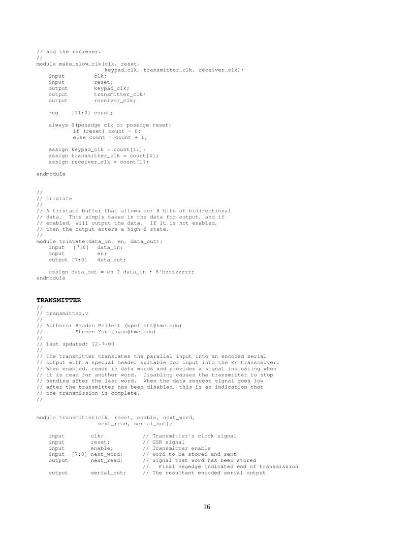
TRANSMITTER // // transmitter.v // // Authors: Braden Pellett ([email protected]) // Steven Yan ([email protected]) // // Last updated: 12-7-00 // // The transmitter translates the parallel input into an encoded serial // output with a special header suitable for input into the RF transceiver. // When enabled, reads in data words and provides a signal indicating when // it is read for another word. Disabling causes the transmitter to stop // sending after the last word. When the data request signal goes low // after the transmitter has been disabled, this is an indication that // the transmission is complete. // module transmitter(clk, reset, enable, next_word, next_read, serial_out); input clk; // Transmitter's clock signal input reset; // GSR signal input enable; // Transmitter enable input [7:0] next_word; // Word to be stored and sent output next_read; // Signal that word has been stored // Final negedge indicated end of transmission output serial_out; // The resultant encoded serial output

17
reg [2:0] state; reg [7:0] current_word; reg next_read; reg [5:0] counter; reg serial_out; reg [11:0] word_sync_sub_bit_header; // // Transmitting FSM // always @(posedge clk or posedge reset) if (reset) begin state <= 'd0; current_word <= 8'b0; next_read <= 0; serial_out <= 1; counter <= 'd1; word_sync_sub_bit_header <= 12'b110110100100; // // Wait to be enabled. // end else if (state == 'd0) begin next_read <= 0; serial_out <= 1; counter <= 'd1; word_sync_sub_bit_header <= 12'b110110100100; if (enable) state <= 'd1; // Start transmission // // When enabled, load in the first word, and start transmit // the header. // end else if (state == 'd1) begin // // The end of the header, so get ready to start sending // the encoded data. // if (counter == 'd55) begin serial_out <= 0; current_word <= next_word; counter[1:0] <= 'd0; counter[4:2] <= 'd1; state <= 'd2; // // After sending 30 low-high signals, send the word sync portion // of the header so the receiver knows what the word alignment // should be. // end else if (counter[5]) begin counter <= counter + 1; serial_out <= word_sync_sub_bit_header[11]; word_sync_sub_bit_header <= word_sync_sub_bit_header[10:0], ~counter[0]; // // Start by sending low-high signals so that the receiver can // get in phase with the transmitter clock. // end else begin counter <= counter + 1; serial_out <= ~serial_out; end // // Send the serial encoded data. // end else if (state == 'd2) begin // // A sub-FSM to encode each bit of the data word // case (counter[1:0]) 'd0: begin // Sub-bit 0: 1
18
serial_out <= 1; next_read <= 1; counter[1:0] <= 'd1; end 'd1: begin // Sub-bit 1: data bit value serial_out <= current_word[7]; counter[1:0] <= 'd2; end 'd2: begin // Sub-bit 2: 0 serial_out <= 0; // // We're at the end of this word, so // deside if and what we need to transmit. // if (counter[4:2] == 'd0) begin // // If we are no longer enabled, stop the transmission // if (~enable) begin counter <= 'd0; state <= 'd4; // // Otherwise, read in the next piece of data, and indicate // that we are doing so. // end else begin counter[1:0] <= 'd0; counter[4:2] <= counter[4:2] + 1; next_read <= 0; current_word <= next_word; end // // Not at the end of the word, so move on to the next bit // end else begin counter[1:0] <= 'd0; counter[4:2] <= counter[4:2] + 1; current_word <= current_word[6:0], 1'b0; end end endcase // // Send a sufficiently long tail of "high" to ensure the receiver knows // the transmission has ended before resetting "next_read" so that the // user knows when the transmitter has finished sending this tail. // end else if (state == 'd4) begin serial_out <= 1; if (counter == 'd24) state <= 'd0; counter <= counter + 1; end endmodule
RECEIVER // // receiver.v // // Authors: Braden Pellett ([email protected]) // Steven Yan ([email protected]) // // Last updated: 12-7-00 // // Sample the serial signal input and decode any incoming data. Output said // data, indicate that a transmission is coming in, and output a signal each // time a new word is available to be read. On the negitive edge of the // incoming transition signal, the packet of data is either complete or // ceased to be readable. // Note: We couldn't seem to get the "incoming_transmission" signal to output
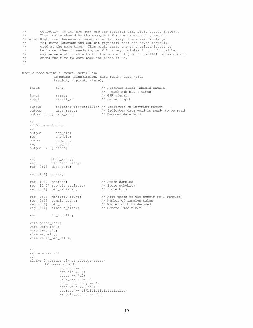
19
// correctly, so for now just use the state[2] diagnostic output instead. // They really should be the same, but for some reason they aren't. // Note: Right now, because of some failed trickery, there are two large // registers (storage and sub_bit_register) that are never actually // used at the same time. This might cause the synthesized layout to // be larger than it needs to, or Xilinx may optimize it out, but either // way we were still able to fit the whole thing onto the FPGA, so we didn't // spend the time to come back and clean it up. // module receiver(clk, reset, serial_in, incoming_transmission, data_ready, data_word, tmp_bit, tmp_cnt, state); input clk; // Receiver clock (should sample // each sub-bit 8 times) input reset; // GSR signal. input serial_in; // Serial input output incoming_transmission; // Indicates an incoming packet output data_ready; // Indicates data_word is ready to be read output [7:0] data_word; // Decoded data word // // Diagnostic data // output tmp_bit; reg tmp_bit; output tmp_cnt; reg tmp_cnt; output [2:0] state; reg data_ready; reg set_data_ready; reg [7:0] data_word; reg [2:0] state; reg [17:0] storage; // Store samples reg [11:0] sub_bit_register; // Store sub-bits reg [7:0] bit_register; // Store bits reg [3:0] majority_count; // Keep track of the number of 1 samples reg [2:0] sample_count; // Number of samples taken reg [3:0] bit_count; // Number of bits decoded reg [5:0] timeout_timer; // General use timer reg is_invalid; wire phase_lock; wire word_lock; wire preamble; wire majority; wire valid_bit_value; // // Receiver FSM // always @(posedge clk or posedge reset) if (reset) begin tmp_cnt <= 0; tmp_bit <= 1; state <= 'd0; data_ready <= 0; set_data_ready <= 0; data_word <= 8'b0; storage <= 18'b111111111111111111; majority_count <= 'b0;

20
sample_count <= 'b0; timeout_timer <= 'b0; bit_count <= 'b0; sub_bit_register <= 'b0; bit_register <= 'b0; is_invalid <= 1; end else begin // // This is just stuff for the diagnostic output... // It doesn't have to exist for proper operation. // tmp_cnt <= ~tmp_cnt; tmp_bit <= serial_in; // // In the first state, we just keep looking for a phase lock, // as defined at the bottom of this file. // if (state == 'd0) begin if (phase_lock) begin state <= 'd1; majority_count <= serial_in; sample_count <= 'd2; timeout_timer <= 'd0; end else storage <= storage[16:0], serial_in; // // Get preamble lock, as defined at the end of this file. // end else if (state == 'd1) begin // // We have gotten 8 samples, so record the majority // as the sub-bit received. // if (sample_count == 'd0) begin sub_bit_register <= sub_bit_register[11:0], majority; timeout_timer <= timeout_timer + 1; sample_count <= sample_count + 1; majority_count <= serial_in; // // If our series of sub-bits shows a proper preamble, // move on. // end else if (preamble) begin state <= 'd2; timeout_timer <= 'd0; // // If we timeout before we see a preamble, return to the // first state and try to resync on a posedge. // end else if (timeout_timer == 'd10) begin state <= 'd0; storage <= 18'b111111111111111111; majority_count <= majority_count + serial_in; sample_count <= sample_count + 1; // // Otherwise, just keep track of how many samples we've // taken since the last sub-bit, and keep track of the // majority. // end else begin majority_count <= majority_count + serial_in; sample_count <= sample_count + 1; end // // Get sync byte lock, as defined at the end of this file. // end else if (state == 'd2) begin // // We have gotten 8 samples, so record the majority // as the sub-bit received. //
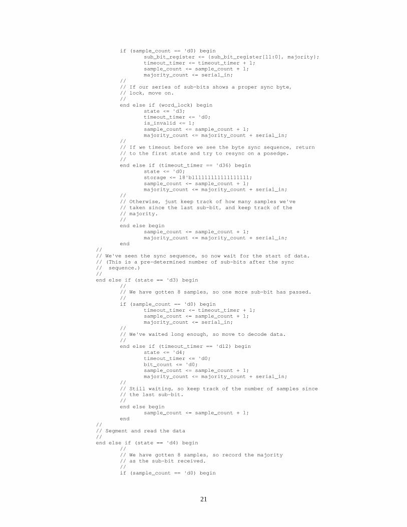
21
if (sample_count == 'd0) begin sub_bit_register <= sub_bit_register[11:0], majority; timeout_timer <= timeout_timer + 1; sample_count <= sample_count + 1; majority_count <= serial_in; // // If our series of sub-bits shows a proper sync byte, // lock, move on. // end else if (word_lock) begin state <= 'd3; timeout_timer <= 'd0; is_invalid <= 1; sample_count <= sample_count + 1; majority_count <= majority_count + serial_in; // // If we timeout before we see the byte sync sequence, return // to the first state and try to resync on a posedge. // end else if (timeout_timer == 'd36) begin state <= 'd0; storage <= 18'b111111111111111111; sample_count <= sample_count + 1; majority_count <= majority_count + serial_in; // // Otherwise, just keep track of how many samples we've // taken since the last sub-bit, and keep track of the // majority. // end else begin sample_count <= sample_count + 1; majority_count <= majority_count + serial_in; end // // We've seen the sync sequence, so now wait for the start of data. // (This is a pre-determined number of sub-bits after the sync // sequence.) // end else if (state == 'd3) begin // // We have gotten 8 samples, so one more sub-bit has passed. // if (sample_count == 'd0) begin timeout_timer <= timeout_timer + 1; sample_count <= sample_count + 1; majority_count <= serial_in; // // We've waited long enough, so move to decode data. // end else if (timeout_timer == 'd12) begin state <= 'd4; timeout_timer <= 'd0; bit_count <= 'd0; sample_count <= sample_count + 1; majority_count <= majority_count + serial_in; // // Still waiting, so keep track of the number of samples since // the last sub-bit. // end else begin sample_count <= sample_count + 1; end // // Segment and read the data // end else if (state == 'd4) begin // // We have gotten 8 samples, so record the majority // as the sub-bit received. // if (sample_count == 'd0) begin

22
sub_bit_register[2:0] <= sub_bit_register[1:0], majority; timeout_timer <= timeout_timer + 1; sample_count <= sample_count + 1; majority_count <= serial_in; // // We have gotten 3 sub-bits, so form these into a // single data-bit, and keep track if we have received // any valid data-bits for this word. // end else if (timeout_timer == 'd3) begin if (set_data_ready) data_ready <= 1; is_invalid <= is_invalid & ~valid_bit_value; set_data_ready <= 0; timeout_timer <= 'd0; sample_count <= sample_count + 1; majority_count <= majority_count + serial_in; bit_count <= bit_count + 1; bit_register <= bit_register[7:0], sub_bit_register[1]; // // We have stored 8 data bits (i.e. a full data word), so // now we need to do something with it. // end else if (bit_count == 'd8) begin // // The entire data word is invalid, so declare this // data packet as over and return to the first state. // if (is_invalid) begin state <= 'd0; data_ready <= 0; set_data_ready <= 0; data_word <= 8'b0; storage <= 18'b111111111111111111; majority_count <= 'b0; sample_count <= 'b0; timeout_timer <= 'b0; bit_count <= 'b0; sub_bit_register <= 'b0; bit_register <= 'b0; is_invalid <= 1; // // We have a at least partially valid word, so output // it in parallel and indicate that a new word // has arrived. // end else begin is_invalid <= 1; data_word <= bit_register; data_ready <= 0; set_data_ready <= 1; bit_count <= 'd0; sample_count <= sample_count + 1; majority_count <= majority_count + serial_in; end // // Otherwise, just keep sampling the input and keeping track // of the majority since the last sub-bit. // end else begin sample_count <= sample_count + 1; majority_count <= majority_count + serial_in; end end end // // A phase lock is when we find a sufficient well defined positive edge // in the sample data. (The old version, commented out right below the // new version, originally looked for a whole square pulse of the proper

23
// width, but this was impractical because it was taking too long for // the data slicer in the RF transceiver module to make properly squared // waves on the output) // assign phase_lock = &(~(storage[13:3] ^ 11'b00000111111)); // assign phase_lock = &(~(storage ^ 18'b100000000111111110)); // // A preamble is the intial low-high transmission // assign preamble = &(~(sub_bit_register[6:0] ^ 7'b0101010)); // // The word lock is used to let the receiver figure out the word alignment. // It consists of sub-bits forming data-bits, namely 1100. // assign word_lock = &(~(sub_bit_register[11:0] ^ 12'b110110100100)); // // The indicator of was the majority is in the 8 samples // of the input: high or low // assign majority = majority_count[3] | majority_count[2]; // // Is the sequence of three sub-bits in the sub-bit register a valid data-bit? // assign valid_bit_value = sub_bit_register[2] & ~sub_bit_register[0]; // // This doesn't work for some reason... we aren't sure why. Just use the state[2] // diagnostic output instead. // assign incoming_transmission = state[2]; endmodule
KEYPAD DECODER // // keypad_decoder.v // // Authors: Braden Pellett ([email protected]) // Steven Yan ([email protected]) // // Last updated: 12-7-00 // // Poll the keypad to see what the user is typing, and output // this information as a ASCII character and a signal saying // there is new data to be read. Refer to the technical report // for how the keypad is arranged and connected. Basically, it is // a 4x4 keypad, where the three top keys on the last column are // shift keys, that allow the first three columns to be selectable // between different ASCII characters. The lower right hand // cell is alway "enter" (value 10). // module keypad_decoder(slowclk, reset_full, rows, cols, shift, read, data); input slowclk; // The clocks for scanning input reset_full; // GSR signal input [3:0] rows; // Read results of polling output [3:0] cols; // Polling outputs output [2:0] shift; // Indicator for shift keys output read; // Indicate for new data output [7:0] data; // Decoded data reg [1:0] state; reg [3:0] cols; reg [6:0] data; reg [6:0] key; reg read;
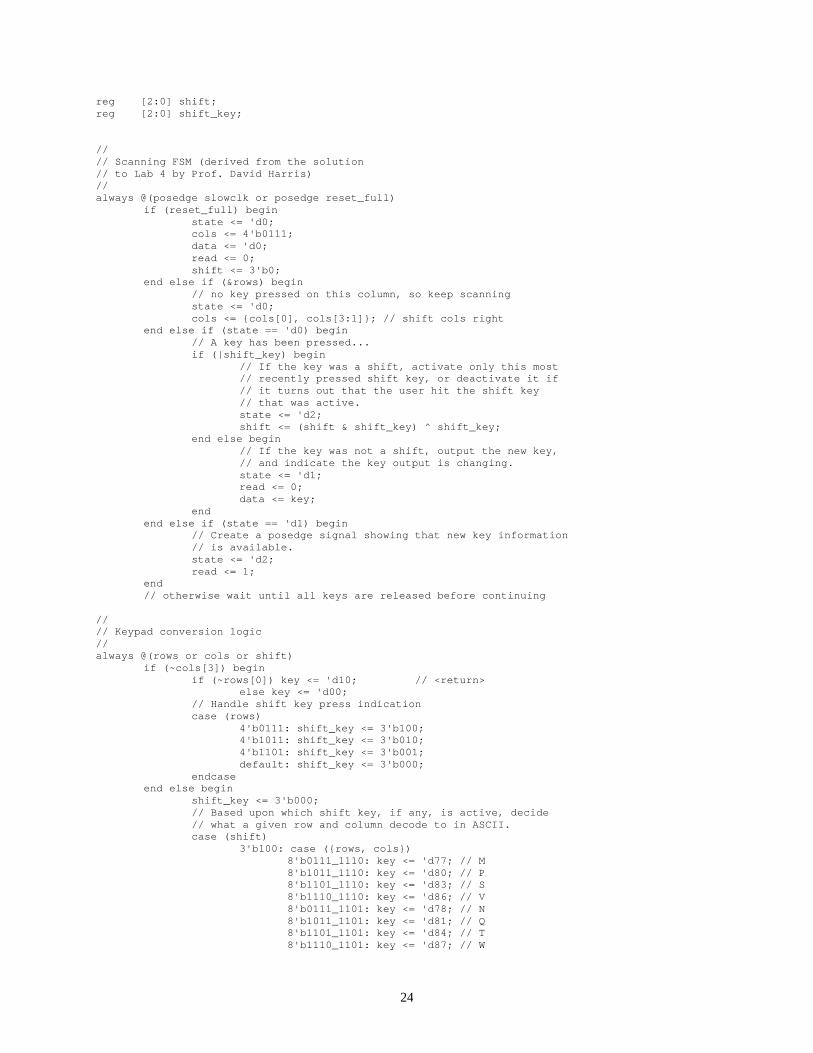
24
reg [2:0] shift; reg [2:0] shift_key; // // Scanning FSM (derived from the solution // to Lab 4 by Prof. David Harris) // always @(posedge slowclk or posedge reset_full) if (reset_full) begin state <= 'd0; cols <= 4'b0111; data <= 'd0; read <= 0; shift <= 3'b0; end else if (&rows) begin // no key pressed on this column, so keep scanning state <= 'd0; cols <= cols[0], cols[3:1]; // shift cols right end else if (state == 'd0) begin // A key has been pressed... if (|shift_key) begin // If the key was a shift, activate only this most // recently pressed shift key, or deactivate it if // it turns out that the user hit the shift key // that was active. state <= 'd2; shift <= (shift & shift_key) ^ shift_key; end else begin // If the key was not a shift, output the new key, // and indicate the key output is changing. state <= 'd1; read <= 0; data <= key; end end else if (state == 'd1) begin // Create a posedge signal showing that new key information // is available. state <= 'd2; read <= 1; end // otherwise wait until all keys are released before continuing // // Keypad conversion logic // always @(rows or cols or shift) if (~cols[3]) begin if (~rows[0]) key <= 'd10; // <return> else key <= 'd00; // Handle shift key press indication case (rows) 4'b0111: shift_key <= 3'b100; 4'b1011: shift_key <= 3'b010; 4'b1101: shift_key <= 3'b001; default: shift_key <= 3'b000; endcase end else begin shift_key <= 3'b000; // Based upon which shift key, if any, is active, decide // what a given row and column decode to in ASCII. case (shift) 3'b100: case (rows, cols) 8'b0111_1110: key <= 'd77; // M 8'b1011_1110: key <= 'd80; // P 8'b1101_1110: key <= 'd83; // S 8'b1110_1110: key <= 'd86; // V 8'b0111_1101: key <= 'd78; // N 8'b1011_1101: key <= 'd81; // Q 8'b1101_1101: key <= 'd84; // T 8'b1110_1101: key <= 'd87; // W

25
8'b0111_1011: key <= 'd79; // O 8'b1011_1011: key <= 'd82; // R 8'b1101_1011: key <= 'd85; // U 8'b1110_1011: key <= 'd88; // X default: key <= 'd0; endcase 3'b010: case (rows, cols) 8'b0111_1110: key <= 'd89; // Y 8'b1011_1110: key <= 'd49; // 1 8'b1101_1110: key <= 'd52; // 4 8'b1110_1110: key <= 'd55; // 7 8'b0111_1101: key <= 'd90; // Z 8'b1011_1101: key <= 'd50; // 2 8'b1101_1101: key <= 'd53; // 5 8'b1110_1101: key <= 'd56; // 8 8'b0111_1011: key <= 'd48; // 0 8'b1011_1011: key <= 'd51; // 3 8'b1101_1011: key <= 'd54; // 6 8'b1110_1011: key <= 'd57; // 9 default: key <= 'd0; endcase 3'b001: case (rows, cols) 8'b0111_1110: key <= 'd46; // . 8'b1011_1110: key <= 'd64; // @ 8'b1101_1110: key <= 'd37; // % 8'b1110_1110: key <= 'd38; // & 8'b0111_1101: key <= 'd63; // ? 8'b1011_1101: key <= 'd35; // # 8'b1101_1101: key <= 'd94; // ^ 8'b1110_1101: key <= 'd40; // ( 8'b0111_1011: key <= 'd33; // ! 8'b1011_1011: key <= 'd36; // $ 8'b1101_1011: key <= 'd32; // <space> 8'b1110_1011: key <= 'd41; // ) default: key <= 'd0; endcase default: case (rows, cols) 8'b0111_1110: key <= 'd65; // A 8'b1011_1110: key <= 'd68; // D 8'b1101_1110: key <= 'd71; // G 8'b1110_1110: key <= 'd74; // J 8'b0111_1101: key <= 'd66; // B 8'b1011_1101: key <= 'd69; // E 8'b1101_1101: key <= 'd72; // H 8'b1110_1101: key <= 'd75; // K 8'b0111_1011: key <= 'd67; // C 8'b1011_1011: key <= 'd70; // F 8'b1101_1011: key <= 'd73; // I 8'b1110_1011: key <= 'd76; // L default: key <= 'd0; endcase endcase end endmodule

26
Appendix B | HC11 Assembly Code * Authors: Steve Yan ([email protected]) * Braden Pellett ([email protected]) * Created: November 14, 2000 * Modified: December 7, 2000 * * Motorola 68HC11 code for RF Wireless text messaging system interface * and LCD module LM016 control. The HC11 is controlled via external * interrupts. * * External Interrupts: * Incoming Data ISR (STRA pin) * Incoming Transmission ISR (IC1I pin (PA2)) * Data Request ISR (IC2I pin (PA1)) * Keypress ISR (IC3I pin (PA0)) ************************************** * Set port and register addresses. * ************************************** REGS EQU $1000 * Base address PORTA EQU $1000 * Output for LCD Control PORTA_I EQU $00 * Output for LCD Control PORTB EQU $1004 * Output for LCD data PORTC EQU $1003 * Bidirectional Port (I/O between HC11 and FPGA) PORTCL EQU $1005 * Latched input for Port C PORTE EQU $100A * Keypad input PIOC EQU $02 * Parallel I/O Control Register (Port C) DDRC EQU $07 * Data Direction register for Port C TCNT EQU $0E * 16-bit built in timer TOC5 EQU $1E * Timer Output Compare 5 (16-bit) TCTL2 EQU $21 * Interrupt signal edge detection TMSK1 EQU $22 * OCxI flags (enables output compare interrupts) TFLG1 EQU $23 * OCxF and ICxF flags (go high after OC match) PACTL EQU $26 * Pulse accumulator control register * * Program data. * MODE EQU $09 * $00 = transmit, $01 = receive, $02 = idle MENU EQU $0A * $00 = main menu, $01 = send msg, $02 = view history LCDROW EQU $0B * Row position of LCD display cursor. LCDCOL EQU $0C * Column position of LCD display cursor. LCDFLG EQU $0D * 1 if max msg size is reached * 7 = expect ctrl char flag, 6 = handshaking flag, 5 = bad data flag, * 4 = incoming message flag, 3 = new message flag, 2 = screen update request IDATFLG EQU $0E TXT_ST EQU $D006 * Starting address of text. * * Message bookkeeping data. (Addresses) *

27
NEWMSG EQU $00 * Stores address of newest message. NUMMSGS EQU $02 * Stores number of messages currently in the history. HSTINDX EQU $03 * Stores value of Y Index Register for view history. DATINDX EQU $05 * Stores value of Y Index Register for rx/tx data. HSTTL EQU $07 * Stores value of last history block. TXHD EQU $19 * Head position of tx data block. HSTHD EQU $3A * Address of first message (1st history block). HSTLMT EQU $00BE * Address of last message (5th history block). * * Constants * M_MAIN EQU $00 M_MSG EQU $01 M_HIST EQU $02 M_SEND EQU $03 CC_STX EQU $02 * STX (start of text) CC_ACK EQU $06 * ACK (postive acknoledgement) * * Init variables. * ORG MODE FCB $02 * Start out idle. FCB $00 * Start in main menu. FCB $00 * LCDROW = 0 FCB $00 * LCDCOL = 0 FCB $00 * LCDFLG = 0 ****************************** * Interrupt vectors. * ****************************** ORG $00E5 * Jump address for Data Request interrupts (IC2). JMP odatisr * Jump to Data Request ISR. ORG $00E8 * Jump address for Incoming Transmsn interrupts (IC1). JMP itxisr * Jump to Incoming Data ISR. ORG $00EE * Jump address for Incoming data interrupts (STRA). JMP idatisr * Jump to Incoming data interrupt. ****************************** * LCD display text storage. * ****************************** ORG TXT_ST MMTXT1 FCC "A. Send message" NULLBLK FCB $00 * Stop character MMTXT2 FCC "B. View history" FCB $00 * Stop character MMTXT3 FCB $7E
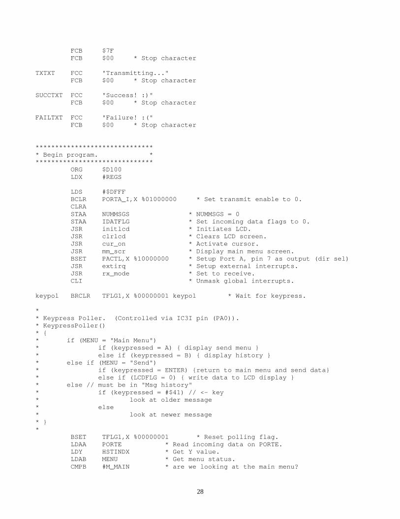
28
FCB $7F FCB $00 * Stop character TXTXT FCC "Transmitting..." FCB $00 * Stop character SUCCTXT FCC "Success! :)" FCB $00 * Stop character FAILTXT FCC "Failure! :(" FCB $00 * Stop character ****************************** * Begin program. * ****************************** ORG $D100 LDX #REGS
LDS #$DFFF BCLR PORTA_I,X %01000000 * Set transmit enable to 0. CLRA STAA NUMMSGS * NUMMSGS = 0 STAA IDATFLG * Set incoming data flags to 0. JSR initlcd * Initiates LCD. JSR clrlcd * Clears LCD screen. JSR cur_on * Activate cursor. JSR mm_scr * Display main menu screen. BSET PACTL,X %10000000 * Setup Port A, pin 7 as output (dir sel) JSR extirq * Setup external interrupts. JSR rx_mode * Set to receive. CLI * Unmask global interrupts.
keypol BRCLR TFLG1,X %00000001 keypol * Wait for keypress. * * Keypress Poller. (Controlled via IC3I pin (PA0)). * KeypressPoller() * * if (MENU = "Main Menu") * if (keypressed = A) display send menu * else if (keypressed = B) display history * else if (MENU = "Send") * if (keypressed = ENTER) return to main menu and send data * else if (LCDFLG = 0) write data to LCD display * else // must be in "Msg history" * if (keypressed = #$41) // <- key * look at older message * else * look at newer message * * BSET TFLG1,X %00000001 * Reset polling flag. LDAA PORTE * Read incoming data on PORTE. LDY HSTINDX * Get Y value. LDAB MENU * Get menu status. CMPB #M_MAIN * are we looking at the main menu?

29
BEQ mmenu * If yes, do main menu keypress logic. CMPB #M_MSG * If not, are we in the send message screen? BEQ write * If so, do send screen keypress logic. BRA hst1 * Else, must be viewing history. mmenu CMPA #$41 * If option A, go to send menu BEQ snd CMPA #$42 * If option B, go to hist menu BEQ hst BRA keyend write CMPA #$0A * Did we press enter? (send key) BNE write2 * If not, just write to display and memory. CLRA STAA 0,Y * Write stop byte ($00) if sending. JSR transmit_scr * Display the transmission message JSR tx_mode * Go into transmit mode LDAA #CC_STX * Get the mesg control chracter STAA PORTC * Store the control character for output LDY #TXHD * Get where the written message is stored STY DATINDX * Store start of rest of data BSET PORTA_I,X %01000000 * Enable transmission JSR rx_mode LDAA #$01 JSR wait * Timeout waiting. CLRA * Give ACCA value of #0 JSR cur2 * Move to (2,0) JSR hsk_hdl * Handle looking for the handshake BRA keyend write2 LDAB LCDFLG BNE keyend * If LCD not full, then write to memory, LCD. STAA 0,Y INY STY HSTINDX JSR writed * Write to LCD display. keyend BRA keypol * Return to polling for next keypress. snd JSR snd_scr BRA keyend hst JSR hst_scr BRA keyend * * If (keypressed == "<--") // view older msgs. * if (Y == HSTHD) * // wrap to end of history memory block. * // display new message. * * else * // shift left in history memory block. * // display new message. * * * Else if (keypressed == "-->") // view newer * if (Y == HSTTL) * // Move to front of history memory block.
30
* // display new message. * * else * // shift right in history memory block. * // display new message. * * Else do nothing * hst1 CMPA #$41 * <- key BNE hst2 LDD HSTINDX CPD #HSTHD * Are we looking at the first history block? BNE mvleft * If not just shift left one history block. wraptl LDY HSTTL * Wrap to rightmost valid memory block. STY HSTINDX BRA disphst mvleft LDD HSTINDX SUBD #33 * Each memory block is 32 chars + 1 stop byte STD HSTINDX LDY HSTINDX BRA disphst hst2 CMPA #$42 * -> key BNE gommenu * If -> key not pressed, ignore the input. LDD HSTINDX CPD HSTTL * Are we looking at the last filled memory block? BNE mvright * If not just shift right one history block. wraphd LDY #HSTHD * Move HSTINDX value to leftmost history block. STY HSTINDX BRA disphst mvright LDD HSTINDX ADDD #33 * Each memory block is 32 chars + 1 stop byte STD HSTINDX LDY HSTINDX BRA disphst gommenu CMPA #$0A * Did we press enter? BNE keyend JSR mm_scr BRA keyend disphst JSR clrlcd JSR display BRA keyend *********************************************************************** * MAIN SUBROUTINES. * *********************************************************************** * * Subroutine: extirq * Desc: Setup all interupts to trigger on active edge of their * respective external signals. IC1I also triggers on negative * edge. Incoming TX (IC1I), Data Request (IC2I), * and Incoming Data (STRA) * Input: None * Output: None

31
* Reg Mod: A, CCR * extirq LDX #REGS LDAA #%00010101 * IC1F, IC2F, IC3F active on pos. STAA TCTL2,X * Write to Timer Control Register 2. LDAA #%00000110 * Enable IC1I, IC2I. STAA TMSK1,X * Enable interrupts. LDAA #%00000111 STAA TFLG1,X * Reset flags. LDAA PIOC,X ORAA #%11000010 * STAF = 1, STAI = 1, EGA = 1 (PIOC) STAA PIOC,X * Generate IRQ on active edge of ext. signal RTS * * Subroutine: txmode * Desc: Setup for transfer of data. * Input: X (points to starts of regs) * Output: None * Reg Mod: A, CCR * * Do not enter tx_mode until Incoming Transmission interrupt is low. tx_mode BRSET PORTA_I,X %00000100 tx_mode BSET DDRC,X $FF * Make PORTC an output. CLR MODE * Set mode to transmit. BSET PACTL,X %10000000 BCLR PACTL,X %01000000 BCLR PORTA_I,X %10000000 * Enable transmitter (clear dir sel) LDAA #$05 * Wait for warmup JSR wait RTS * * Subroutine: rxmode * Desc: Setup for reception of data. * Input: X (points to start of regs) * Output: None * Reg Mod: A, CCR * * Continue only if incoming data isr pin is low and enable transmit is low. rx_mode BRCLR PORTA_I,X %01000010 cont_rx BRA rx_mode cont_rx CLR DDRC,X * Make PORTC an input. LDAA #$01 * Set mode to receive STAA MODE BSET PORTA_I,X %10000000 * Enable receiver (set dir sel) LDAA #$05 * Wait for switching. JSR wait exit RTS ************************ * Subtroutine: wait * Desc: Wait for acc[A] milliseconds * Input: A * Output: None * Reg Mod: A, CCR
32
* wait PSHX wait_spin1 LDX #2000 wait_spin2 DEX BNE wait_spin2 DECA BNE wait_spin1 PULX RTS ********************************************************* * INTERRUPT SERVICE ROUTINES (ISR). * ********************************************************* * * Incoming Data ISR. (Controlled via STRA pin). * idatisr LDX #REGS LDAA PIOC,X * Reset STAF bit. LDAA PORTCL * Read data from latched PORTC data. BRSET IDATFLG %00100000 exit8 * If bad data, exit. BRSET IDATFLG %10000000 cchr1 * Else if expecting control char, BRSET IDATFLG %00010000 hdl_msg * Else if reading message, BRA exit8 * Else, exit and ignore the data * Else do incoming message handling. hdl_msg LDY DATINDX * Load rx position into Y STAA 0,Y * Write data to memory. INY STY DATINDX * Increment DATINDX, and store in memory exit8 RTI cchr1 BCLR IDATFLG %10000000 * Reset control character flag. CMPA #CC_STX * If the control character signifies msg, BNE cchr2 JSR calhblk * Calibrate history memory block. BSET IDATFLG %00010000 * Set 4th bit high (signifies mesg) RTI cchr2 CMPA #CC_ACK * Else if control character is handshake, BNE discard BSET IDATFLG %01000000 * Set 6th bit high (signifies handshake) RTI discard BSET IDATFLG %00100000 * Else RTI * Set 5th bit high (signifies bad data). * * Incoming Transmission ISR. (Controlled via IC1I pin (PA2)) * * If interrupted on posedge, setup DATINDX to for recording the incoming * data in the history memory blocks. Also, set PORTC as an input.
33
* * If interrupted on negedge, then the transmission is either complete or has * been interrupted. * itxisr LDX #REGS LDAA #%00000100 * Want to reset IC1F. STAA TFLG1,X * Reset flags. LDAA TCTL2,X CMPA #%00010101 * Are we current set at neg or posedge? BNE negedge posedge LDAA #%00100101 * Make IC1F active on negedge. STAA TCTL2,X BSET IDATFLG %10000000 * Expect control character. BRA exit3 negedge LDAA #%00010101 * Make IC1F active on posedge again. STAA TCTL2,X BCLR IDATFLG %00100000 * Reset bad data flag BRSET IDATFLG %00010000 tx_hsk * If msg received, need to handshake BRA exit3 * Otherwise exit tx_hsk LDY DATINDX CLR 0,Y * Place stop byte at end of mesg. BCLR IDATFLG %00010000 * Clear incoming mesg flag BSET IDATFLG %00001000 * Set new message flag JSR tx_mode * Go into tx mode to send handshake LDAA #CC_ACK * Get the handshake control chracter STAA PORTC * Store the control character for output LDY #NULLBLK * Stored null character STY DATINDX * Store start of rest of data CLI * Allow for a nested inturrupt BSET PORTA_I,X %01000000 * Enable transmission LDAB MENU * Get menu status. CMPB #M_MAIN * are we looking at the main menu? BNE nupd_mm * If not, don't update it. JSR mm_scr2 * Update the main menu, if we are there nupd_mm JSR rx_mode * enter rx mode when tx completes exit3 RTI * * Subroutine: calhblk * Desc: Finds the next history memory block for storage of * the incoming message. * Input: None * Output: None * Reg Mod: A, Y, CCR * calhblk PSHX LDAA NUMMSGS * Check NUMMSGS BNE chklmt * If (NUMMSGS == 0) INCA * Increment NUMMSGS STAA NUMMSGS * LDX #HSTHD * Set to write at the first hist. blk. STX DATINDX * STX HSTTL * Make the tail the head. STX NEWMSG
34
BRA exit4 chklmt LDD NEWMSG * CPD #HSTLMT * Else if (NEWMSG == HSTLMT) BNE default * LDX #HSTHD * Wrap around to front of history blks. STX DATINDX STX NEWMSG BRA exit4 default LDD NEWMSG * Else ADDD #33 * Shift right by one history block. STD NEWMSG * Record new position of newest msg. STD DATINDX * Record new position. LDY #HSTLMT CPY HSTTL BEQ exit4 STD HSTTL * Modify tail position. exit4 PULX RTS * * Data Request ISR. (Controlled via IC2I pin (PA1)). * odatisr LDX #REGS LDY DATINDX LDAA 0,Y BNE cont disable LDX #REGS BCLR PORTA_I,X %01000000 * Disable transmission pin on FPGA BRA exit6 cont STAA PORTC INY STY DATINDX exit6 BSET TFLG1,X %00000010 * reset IC2F RTI *********************************************************************** * All LCD control subroutines adapted from * * "Digital Alarm Clock", Jason Fong, Fernando Mattos. * * http://www3.hmc.edu/~harris/class/e155/projects99/alarmclock1.pdf * *********************************************************************** * * INITLCD subroutine. * initlcd LDAA #$38 JSR writec LDAA #$38 JSR writec LDAA #$38 JSR writec LDAA #$06 JSR writec LDAA #$0C JSR writec RTS

35
* * CLRLCD subroutine. * clrlcd LDAA #$01 * Clear the LCD screen. JSR writec CLR LCDROW * Set LCD coordinates. CLR LCDCOL CLR LCDFLG * Clear LCDFLG. RTS * * CURSORON subroutine. * cur_on LDAA #$0D * Activate cursor. JSR writec RTS * * CURSOROFF subroutine. * cur_off LDAA #$0C JSR writec RTS * * CUR1 subroutine. * Moves the LCD cursor to a column (designated in ACCA) in row 1. * cur1 STAA LCDCOL LDAB #1 STAB LCDROW ADDA #$7F JSR writec RTS * * CUR2 subroutine. * Moves the LCD cursor to a column (designated in ACCA) in row 2. * cur2 STAA LCDCOL LDAB #2 STAB LCDROW ADDA #$BF JSR writec RTS * * SUBROUTINE TO WRITE INSTRUCTIONS TO THE LCD DISPLAY MODULE. * Bit 5 -> R/W, Bit 4 -> RS, Bit 3 -> E * writec * * R/W=0, RS=0, E=0 BCLR PORTA_I,X %00111000 STAA PORTB * Write controls * * E=1 BSET PORTA_I,X %00001000 * * E=0

36
BCLR PORTA_I,X %00001000 * * R/W=1 BSET PORTA_I,X %00100000 LDAA #10 * Delay for 10 ms JSR wait RTS * * SUBROUTINE TO WRITE DATA TO THE LCD DISPLAY MODULE. * Writes characters to the lcd screen at the cursor position. * writed * * R/W=0, RS=1, E=0 BSET PORTA_I,X %00010000 BCLR PORTA_I,X %00101000 STAA PORTB * Write character * * E=1 BSET PORTA_I,X %00001000 * * E=0 BCLR PORTA_I,X %00001000 * * R/W=1 BSET PORTA_I,X %00100000 LDAA #2 * Delay for 2ms JSR wait INC LCDCOL * Wrote a char, so increment column position. LDAA LCDCOL CMPA #$10 * If we see 16, we're at the right boundary. BNE exit5 testrow LDAA LCDROW * If row is 2, then we can't write anymore. CMPA #$02 * If row is 1, then wrap to (2,0) BNE wrap LDAA #1 * Set max flag STAA LCDFLG BRA exit5 wrap CLRA JSR cur2 exit5 RTS *********************************************** * LCD screen subroutines. *********************************************** * * DISPLAY subroutine. * LCD menu options are hard-coded into specific locations in memory. * Prior to calling the display subroutine, the location for the menu * option is loaded into Y. Display increments through memory after * the location in Y until it hits the designated stop character ($00). * display loopd LDAA 0,Y * Grab current character from menu position. BEQ dispend * If character is $00 (stop byte), terminate. JSR writed INY BRA display dispend RTS
37
mm_scr JSR clrlcd JSR cur_off * Hide cursor. LDAA #M_MAIN STAA MENU * Set menu mode to "main menu" ($00) LDY #MMTXT1 * Set Y to start of main menu screen text (line 1). JSR display * Display the text. CLRA * Give ACCA value of #0 JSR cur2 * Move to (2,0) LDY #MMTXT2 * Set Y to start of main menu screen text (line 2). JSR display * Display the text. mm_scr2 BRCLR IDATFLG %00001000 mm_scr3 * Don't indicate new message BCLR IDATFLG %00001000 LDAA #$03 JSR cur2 LDAA #$7E JSR writed LDAA #$10 JSR cur2 LDAA #$7F JSR writed mm_scr3 RTS snd_scr JSR clrlcd JSR cur_on LDAA #M_MSG STAA MENU * Set menu mode to "send screen" ($01) LDY #TXHD * Set Y to increment across TX memory block STY HSTINDX * Store Y RTS transmit_scr JSR clrlcd LDAA #M_SEND STAA MENU LDY #TXTXT JSR display JSR cur_off RTS hst_scr LDAB PORTE * Get keypress. LDAA NUMMSGS * If no messages in queue, do nothing. BEQ exit2 LDY NEWMSG * Else, load the newest message into the screen. STY HSTINDX * display needs to have starting address of data. JSR clrlcd JSR display LDAA #M_HIST * Set MENU to "Message History". STAA MENU * The keypress ISR relies on this data to correctly exit2 RTS * interpret keypresses. *

38
* This is here in subroutine form only because we were branching * out of range in the main key poller. * hsk_hdl BRSET IDATFLG %01000000 succtx * Check if handshake received. * * If no handshake received, give failure message. LDY #FAILTXT * Set Y to start of fail text. JSR display * Display the text. JSR cur_off * Hide cursor. BRA gomain succtx * * If handshake received, give successful message. LDY #SUCCTXT * Set Y to start of succeed text. JSR display * Display the text. BCLR IDATFLG %01000000 * Clear handshake flag gomain BRCLR TFLG1,X %00000001 gomain * Wait for keypress. BSET TFLG1,X %00000001 * Reset polling flag. JSR mm_scr RTS

39
Appendix C | Keypad Layout
The keypad layout is able to use more than 16 characters by using a shifting technique to switch between different sets of characters. The shift keys are the upper three keys on the rightmost column of the keypad. The dark black dot in the diagrams signify which shift key activates which set of characters.
A B C
D E F
G H I
J K L
M N O
P Q R
S T U
V W X
Y Z 0
1 2 3
4 5 6
7 8 9
. ? !
@ # $
% ^ sp
& ( )

40
Appendix D | FPGA Pinout
Pinout by Pin Name: +------------------------------------------------+-----------+--------------+ | Pin Name | Direction | Pin Number | +------------------------------------------------+-----------+--------------+ | SC_rxdata | INPUT | P18 | | SC_rxen | OUTPUT | P10 | | SC_txdata | OUTPUT | P8 | | SC_txen | OUTPUT | P9 | | clk | INPUT | P13 | | keypad_cols<0> | OUTPUT | P36 | | keypad_cols<1> | OUTPUT | P35 | | keypad_cols<2> | OUTPUT | P29 | | keypad_cols<3> | OUTPUT | P28 | | keypad_data_port<0> | OUTPUT | P70 | | keypad_data_port<1> | OUTPUT | P69 | | keypad_data_port<2> | OUTPUT | P68 | | keypad_data_port<3> | OUTPUT | P67 | | keypad_data_port<4> | OUTPUT | P66 | | keypad_data_port<5> | OUTPUT | P65 | | keypad_data_port<6> | OUTPUT | P62 | | keypad_data_port<7> | OUTPUT | P61 | | keypad_data_ready | OUTPUT | P72 | | keypad_rows<0> | INPUT | P38 | | keypad_rows<1> | INPUT | P39 | | keypad_rows<2> | INPUT | P40 | | keypad_rows<3> | INPUT | P44 | | receiver_clk | OUTPUT | P46 | | receiver_data_ready | OUTPUT | P59 | | receiver_incoming_transmission | OUTPUT | P45 | | reset_L | INPUT | P19 | | shift_L<0> | OUTPUT | P25 | | shift_L<1> | OUTPUT | P24 | | shift_L<2> | OUTPUT | P23 | | tmp_bit | OUTPUT | P48 | | tmp_cnt | OUTPUT | P47 | | tmp_state<0> | OUTPUT | P51 | | tmp_state<1> | OUTPUT | P50 | | tmp_state<2> | OUTPUT | P49 | | transceiver_data_port<0> | BIDIR | P84 | | transceiver_data_port<1> | BIDIR | P83 | | transceiver_data_port<2> | BIDIR | P82 | | transceiver_data_port<3> | BIDIR | P81 | | transceiver_data_port<4> | BIDIR | P80 | | transceiver_data_port<5> | BIDIR | P79 | | transceiver_data_port<6> | BIDIR | P78 | | transceiver_data_port<7> | BIDIR | P77 | | transceiver_direction_select | INPUT | P56 | | transmitter_data_request | OUTPUT | P58 | | transmitter_enable | INPUT | P57 | +------------------------------------------------+-----------+--------------+

41
Appendix E | Final Product