RF Power LDMOS Transistor - NXP...
16
RF Power LDMOS Transistor N--Channel Enhancement--Mode Lateral MOSFET The 250 W CW RF power transistor is designed for industrial, scientific, medical (ISM) and industrial heating applications at 2450 MHz. This device is suitable for use in CW, pulse and linear applications. This high gain, high efficiency rugged device is targeted to replace industrial magnetrons and will provide longer life and easier servicing. Typical Performance: In 2400–2500 MHz reference circuit, V DD = 32 Vdc Frequency (MHz) Signal Type P in (W) G ps (dB) D (%) P out (W) 2400 CW 9.0 14.5 55.5 255 2450 9.0 14.7 54.8 263 2500 9.0 14.3 55.5 242 Load Mismatch/Ruggedness Frequency (MHz) Signal Type VSWR P in (W) Test Voltage Result 2450 CW > 10:1 at all Phase Angles 14 (3 dB Overdrive) 32 No Device Degradation Features Characterized with series equivalent large--signal impedance parameters Internally matched for ease of use Qualified up to a maximum of 32 V DD operation Integrated high performance ESD protection Typical Applications Industrial heating and drying Material welding Plasma lighting Scientific Medical: skin treatment, blood therapy, electrosurgery Document Number: MRF7S24250N Rev. 1, 9/2016 NXP Semiconductors Technical Data OM--780--2L PLASTIC 2450 MHz, 250 W, 32 V RF POWER LDMOS TRANSISTOR MRF7S24250N Figure 1. Pin Connections (Top View) Drain Note: Exposed backside of the package is the source terminal for the transistor. 1 2 Gate 2016 NXP B.V.
Transcript of RF Power LDMOS Transistor - NXP...

MRF7S24250N
1RF Device DataNXP Semiconductors
RF Power LDMOS TransistorN--Channel Enhancement--Mode Lateral MOSFETThe 250 W CW RF power transistor is designed for industrial, scientific,
medical (ISM) and industrial heating applications at 2450 MHz. This device issuitable for use in CW, pulse and linear applications. This high gain, highefficiency rugged device is targeted to replace industrial magnetrons and willprovide longer life and easier servicing.
Typical Performance: In 2400–2500 MHz reference circuit, VDD = 32 Vdc
Frequency(MHz) Signal Type
Pin(W)
Gps(dB)
D(%)
Pout(W)
2400 CW 9.0 14.5 55.5 255
2450 9.0 14.7 54.8 263
2500 9.0 14.3 55.5 242
Load Mismatch/Ruggedness
Frequency(MHz) Signal Type VSWR
Pin(W)
TestVoltage Result
2450 CW > 10:1at all PhaseAngles
14(3 dB
Overdrive)
32 No DeviceDegradation
Features
Characterized with series equivalent large--signal impedance parameters Internally matched for ease of use Qualified up to a maximum of 32 VDD operation Integrated high performance ESD protection
Typical Applications
Industrial heating and drying Material welding Plasma lighting Scientific Medical: skin treatment, blood therapy, electrosurgery
Document Number: MRF7S24250NRev. 1, 9/2016
NXP SemiconductorsTechnical Data
OM--780--2LPLASTIC
2450 MHz, 250 W, 32 VRF POWER LDMOS TRANSISTOR
MRF7S24250N
Figure 1. Pin Connections
(Top View)
Drain
Note: Exposed backside of the package isthesource terminal for the transistor.
12Gate
2016 NXP B.V.

2RF Device Data
NXP Semiconductors
MRF7S24250N
Table 1. Maximum Ratings
Rating Symbol Value Unit
Drain--Source Voltage VDSS –0.5, +65 Vdc
Gate--Source Voltage VGS –6.0, +10 Vdc
Storage Temperature Range Tstg –65 to +150 C
Case Operating Temperature Range TC –40 to +150 C
Operating Junction Temperature Range (1,2) TJ –40 to +225 C
Total Device Dissipation @ TC = 25CDerate above 25C
PD 7693.85
WW/C
Table 2. Thermal Characteristics
Characteristic Symbol Value (2,3) Unit
Thermal Resistance, Junction to CaseCW: Case Temperature 98C, 250 W CW, IDQ = 100 mA, 2450 MHz
RJC 0.26 C/W
Thermal Impedance, Junction to CasePulse: Case Temperature 53C, 250 W Peak, 100 sec Pulse Width, 10% DutyCycle, IDQ = 100 mA, 2450 MHz
ZJC 0.024 C/W
Table 3. ESD Protection Characteristics
Test Methodology Class
Human Body Model (per JESD22--A114) 2, passes 2500 V
Machine Model (per EIA/JESD22--A115) B, passes 250 V
Charge Device Model (per JESD22--C101) IV, passes 2000 V
Table 4. Moisture Sensitivity Level
Test Methodology Rating Package Peak Temperature Unit
Per JESD22--A113, IPC/JEDEC J--STD--020 3 260 C
Table 5. Electrical Characteristics (TA = 25C unless otherwise noted)
Characteristic Symbol Min Typ Max Unit
Off Characteristics
Zero Gate Voltage Drain Leakage Current(VDS = 65 Vdc, VGS = 0 Vdc)
IDSS — — 10 Adc
Zero Gate Voltage Drain Leakage Current(VDS = 32 Vdc, VGS = 0 Vdc)
IDSS — — 2 Adc
Gate--Source Leakage Current(VGS = 5 Vdc, VDS = 0 Vdc)
IGSS — — 1 Adc
On Characteristics
Gate Threshold Voltage(VDS = 10 Vdc, ID = 303 Adc)
VGS(th) — 1.2 — Vdc
Gate Quiescent Voltage(VDD = 30 Vdc, ID = 100 mAdc, Measured in Functional Test)
VGS(Q) 1.1 1.6 2.1 Vdc
Drain--Source On--Voltage(VGS = 10 Vdc, ID = 3.7 Adc)
VDS(on) — 0.2 — Vdc
Dynamic Characteristics (4)
Reverse Transfer Capacitance(VDS = 32 Vdc 30 mV(rms)ac @ 1 MHz, VGS = 0 Vdc)
Crss — 4.3 — pF
1. Continuous use at maximum temperature will affect MTTF.2. MTTF calculator available at http://www.nxp.com/RF/calculators.3. Refer to AN1955, Thermal Measurement Methodology of RF Power Amplifiers. Go to http://www.nxp.com/RF and search for AN1955.4. Part internally matched both on input and output.
(continued)

MRF7S24250N
3RF Device DataNXP Semiconductors
Table 5. Electrical Characteristics (TA = 25C unless otherwise noted) (continued)
Characteristic Symbol Min Typ Max Unit
Functional Tests (In NXP Test Fixture, 50 ohm system) VDD = 30 Vdc, IDQ = 100 mA, Pin = 9 W Peak (0.9 W Avg.), f = 2450 MHz,100 sec Pulse Width, 10% Duty Cycle
Output Power Pout 237 256 319 W
Drain Efficiency D 48 50 — %
Input Return Loss IRL — –15.0 –8.5 dB
Table 6. Ordering Information
Device Tape and Reel Information Package
MRF7S24250NR3 R3 Suffix = 250 Units, 32 mm Tape Width, 13--inch Reel OM--780--2L

4RF Device Data
NXP Semiconductors
MRF7S24250N
TYPICAL CHARACTERISTICS
0
25
0 2010
VDS, DRAIN--SOURCE VOLTAGE (VOLTS)
Figure 2. Capacitance versus Drain--Source Voltage
C,CAPACITANCE(pF)
10
Crss
Measured with 30 mV(rms)ac @ 1 MHzVGS = 0 Vdc
Note: Each side of device measured separately.
30
25 30 35
5
15
20
155

MRF7S24250N
5RF Device DataNXP Semiconductors
2400–2500 MHz REFERENCE CIRCUIT — 2 3 (5.1 cm 7.6 cm)
Table 7. 2400–2500 MHz Performance (In NXP Reference Circuit, 50 ohm system)VDD = 32 Vdc, IDQ = 100 mA, TC = 25C
Frequency(MHz)
Pin(W)
Gps(dB)
D(%)
Pout(W)
2400 9.0 14.5 55.5 255
2450 9.0 14.7 54.8 263
2500 9.0 14.3 55.5 242
Table 8. Load Mismatch/Ruggedness (In NXP Reference Circuit)
Frequency(MHz)
SignalType VSWR
Pin(W) Test Voltage, VDD Result
2450 CW > 10:1 at allPhase Angles
14(3 dB Overdrive)
32 No DeviceDegradation

6RF Device Data
NXP Semiconductors
MRF7S24250N
2400–2500 MHz REFERENCE CIRCUIT — 2 3 (5.1 cm 7.6 cm)
Figure 3. MRF7S24250N Reference Circuit Component Layout — 2400–2500 MHz
MRF7S24250NRev. 0
D68993
C2 C3
R1
C1
C6
C4*C5*
C7 C8
C9
C10
Q1
*C4 and C5 are mounted vertically.
Table 9. MRF7S24250N Reference Circuit Component Designations and Values — 2400–2500 MHzPart Description Part Number Manufacturer
C1, C3, C4, C5, C6, C7, C8 27 pF Chip Capacitors ATC600F270JT250XT ATC
C2, C9 10 F Chip Capacitors GRM32ER61H106KA12L Murata
C10 220 F, 50 V Electrolytic Capacitor 227CKE050M Illinois Capacitor
Q1 RF Power LDMOS Transistor MRF7S24250NR3 NXP
R1 10 , 1/4 W Chip Resistor CRCW120610R0FKEA Vishay
PCB Rogers RT6035HTC, 0.030, r = 3.66 D68993 MTL

MRF7S24250N
7RF Device DataNXP Semiconductors
TYPICAL CHARACTERISTICS — 2400–2500 MHzREFERENCE CIRCUIT
2400
Gps
f, FREQUENCY (MHz)
Figure 4. Power Gain, Drain Efficiency and Output Powerversus Frequency at a Constant Input Power
13.5
15.25
200
60
55
50
45
275
250
225
D,DRAIN
EFFICIENCY(%)D
Gps,POWER
GAIN(dB)
15
14.5
2440 2480
P out,OUTPUT
POWER
(WATTS)
VDD = 32 VdcPin = 9.0 WIDQ = 100 mA
Pout
14.75
14.25
14
13.75
24602420 2500
00
VGS, GATE--SOURCE VOLTAGE (VOLTS)
Figure 5. Output Power versus Gate--Source Voltage
300
0.5 1 1.5 2
250
50
200
100
P out,OUTPUTPOWER
(WATTS)
f = 2450 MHz
VDD = 32 VdcPin = 9.0 W
00
Detail A
f = 2450 MHzDetail A
VDD = 32 VdcPin = 4.5 W
P out,OUTPUTPOWER
(WATTS)
VGS, GATE--SOURCE VOLTAGE (VOLTS)
150
VDD = 32 VdcPin = 4.5 W
1.210.4
100
125
150
2.5
75
50
0.2 0.6 0.8
VDD = 32 VdcPin = 9.0 W
25
Figure 6. Power Gain, Drain Efficiency and Input Powerversus Output Power and Frequency
Pout, OUTPUT POWER (WATTS)
Gps,POWER
GAIN(dB)
12
15
14
11 500
Gps15
20
0
5
18
17
16
5
50
65
100
Pin
13
P in,INPUT
POWER
(WATTS)
19
11
10
35
20
10
D,DRAIN
EFFICIENCY(%)f = 2500 MHz
2450 MHz 2400 MHz
2500 MHz
2450 MHz
2400 MHz
2400 MHz2450 MHz
2500 MHz
VDD = 32 VdcIDQ = 100 mA
D

8RF Device Data
NXP Semiconductors
MRF7S24250N
2400–2500 MHz REFERENCE CIRCUIT
Zo = 10
Zsource
f = 2400 MHzf = 2500 MHz
Zload
f = 2400 MHz
f = 2500 MHz
fMHz
Zsource
Zload
2400 1.76 – j5.76 1.49 – j2.45
2450 1.66 – j5.50 1.43 – j2.18
2500 1.56 – j5.23 1.36 – j1.90
Zsource = Test circuit impedance as measured fromgate to ground.
Zload = Test circuit impedance as measured fromdrain to ground.
Figure 7. Series Equivalent Source and Load Impedance — 2400–2500 MHz
InputMatchingNetwork
DeviceUnderTest
OutputMatchingNetwork
Zsource Zload
5050

MRF7S24250N
9RF Device DataNXP Semiconductors
2450 MHz NARROWBAND PRODUCTION TEST FIXTURE — 3 5 (7.6 cm 12.7 cm)
Table 10. 2450 MHz Narrowband Performance (In NXP Test Fixture, 50 ohm system) VDD = 30 Vdc, IDQ = 100 mA,Pin = 9 W Peak (0.9 W Avg.), f = 2450 MHz, 100 sec Pulse Width, 10% Duty Cycle
Characteristic Symbol Min Typ Max Unit
Output Power Pout — 256 — W
Drain Efficiency D — 49.0 — %
Input Return Loss IRL — –17 –9 dB

10RF Device Data
NXP Semiconductors
MRF7S24250N
2450 MHz NARROWBAND PRODUCTION TEST FIXTURE — 3 5 (7.6 cm 12.7 cm)
Figure 8. MRF7S24250N Narrowband Test Circuit Component Layout — 2450 MHz
MRF7S24250NRev. 0
C3 C4
C1R1
C2
C13
C14
C5
C6
C7 C8
C9
C10
C11
C12
CUTOUTAREA
Table 11. MRF7S24250N Narrowband Test Circuit Component Designations and Values — 2450 MHzPart Description Part Number Manufacturer
C1, C5, C12 10 F Chip Capacitors C5750X7S2A106M230KB TDK
C2, C6, C11 3 pF Chip Capacitors ATC100B3R0CT500XT ATC
C3 7.5 pF Chip Capacitor ATC100B7R5CT500XT ATC
C4 1.5 pF Chip Capacitor ATC100B1R5BT500XT ATC
C7 0.3 pF Chip Capacitor ATC100B0R3BT500XT ATC
C8 1.5 pF Chip Capacitor ATC100B1R5BT500XT ATC
C9. C10 8.2 pF Chip Capacitors ATC100B8R2CT500XT ATC
C13, C14 470 F, 100 V Electrolytic Capacitors MCGPR100V477M16X32-RH Multicomp
R1 5.9 , 1/4 W Chip Resistor CRCW12065R90FKEA Vishay
PCB Taconic RF35, 0.030, r = 3.5 — MTL
fMHz
Zsource
Zload
2450 1.96 – j5.61 1.55 – j1.76
Zsource = Test circuit impedance as measured fromgate to ground.
Zload = Test circuit impedance as measured fromdrain to ground.
Figure 9. Narrowband Series Equivalent Source and Load Impedance — 2450 MHz
InputMatchingNetwork
DeviceUnderTest
OutputMatchingNetwork
Zsource Zload
5050

MRF7S24250N
11RF Device DataNXP Semiconductors
Figure 10. PCB Pad Layout for OM--780--2L
1. Slot dimensions are minimum dimensions and exclude milling tolerances
2X SOLDER PADS
Inches(mm)
0.800(20.32)
0.409(1)
(10.39)
0.540(13.72)
0.815(1)
(20.70)
0.389(1)
(9.88)
12RF Device Data
NXP Semiconductors
MRF7S24250N
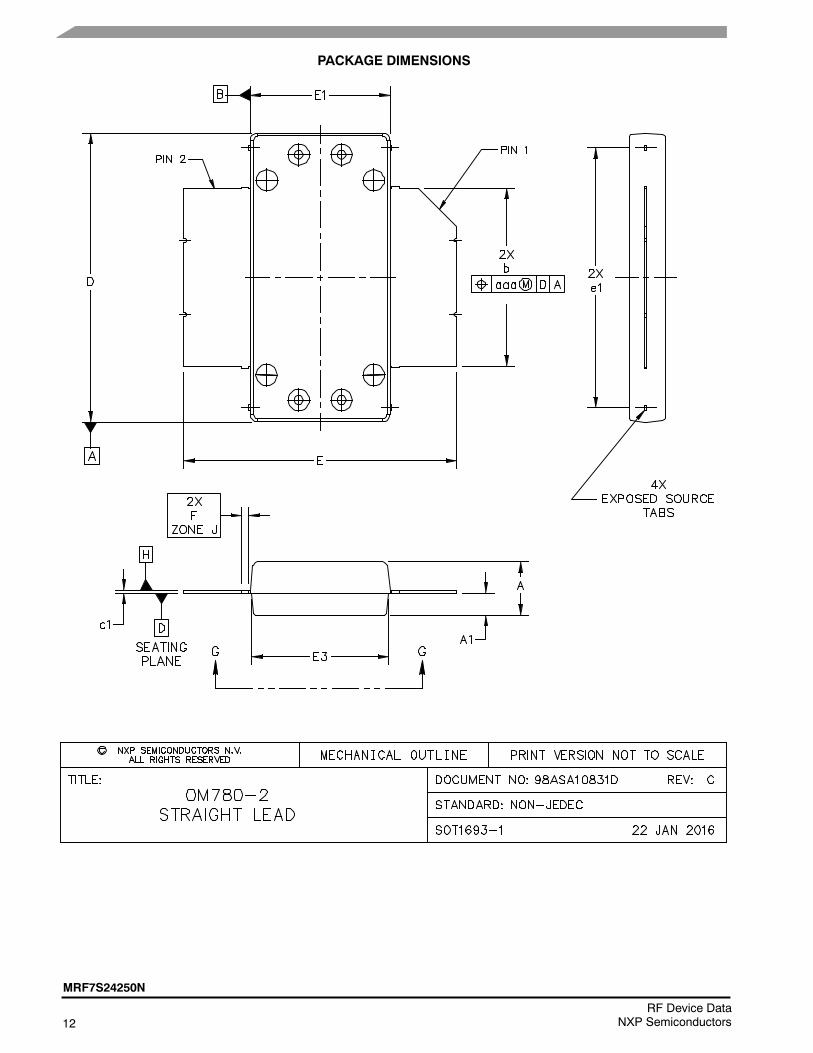
PACKAGE DIMENSIONS

MRF7S24250N
13RF Device DataNXP Semiconductors

14RF Device Data
NXP Semiconductors
MRF7S24250N
MRF7S24250N
15RF Device DataNXP Semiconductors
PRODUCT DOCUMENTATION, SOFTWARE AND TOOLS
Refer to the following resources to aid your design process.
Application Notes
AN1907: Solder Reflow Attach Method for High Power RF Devices in Over--Molded Plastic Packages AN1955: Thermal Measurement Methodology of RF Power Amplifiers AN3789: Clamping of High Power RF Transistors and RFICs in Over--Molded Plastic PackagesEngineering Bulletins EB212: Using Data Sheet Impedances for RF LDMOS Devices
White Paper
RFPLASTICWP: Designing with Plastic RF Power TransistorsSoftware Electromigration MTTF Calculator RF High Power Model .s2p FileDevelopment Tools
Printed Circuit Boards
To Download Resources Specific to a Given Part Number:1. Go to http://www.nxp.com/RF
2. Search by part number
3. Click part number link
4. Choose the desired resource from the drop down menu
REVISION HISTORY
The following table summarizes revisions to this document.
Revision Date Description
0 Aug. 2015 Initial Release of Data Sheet
1 Sept. 2016 Table 2, Thermal Characteristics: added Thermal Impedance ZJC data, p. 2
Functional Tests table: table values updated to reflect current test data results. Added Min and Max values,p. 3

16RF Device Data
NXP Semiconductors
MRF7S24250N
Information in this document is provided solely to enable system and softwareimplementers to use NXP products. There are no express or implied copyright licensesgranted hereunder to design or fabricate any integrated circuits based on the informationin this document. NXP reserves the right to make changes without further notice to anyproducts herein.
NXP makes no warranty, representation, or guarantee regarding the suitability of itsproducts for any particular purpose, nor does NXP assume any liability arising out of theapplication or use of any product or circuit, and specifically disclaims any and all liability,including without limitation consequential or incidental damages. “Typical” parametersthat may be provided in NXP data sheets and/or specifications can and do vary indifferent applications, and actual performance may vary over time. All operatingparameters, including “typicals,” must be validated for each customer application bycustomer’s technical experts. NXP does not convey any license under its patent rightsnor the rights of others. NXP sells products pursuant to standard terms and conditions ofsale, which can be found at the following address: nxp.com/SalesTermsandConditions.
NXP, the NXP logo, Freescale, and the Freescale logo are trademarks of NXP B.V.All other product or service names are the property of their respective owners.E 2016 NXP B.V.
How to Reach Us:
Home Page:nxp.com
Web Support:nxp.com/support
Document Number: MRF7S24250NRev. 1, 9/2016