RF Circuit Synthesis for Physical Wireless Design · RF Circuit Synthesis for Physical ... •When...
59
RF Circuit Synthesis for Physical Wireless Design
Transcript of RF Circuit Synthesis for Physical Wireless Design · RF Circuit Synthesis for Physical ... •When...

RF Circuit Synthesis for
Physical Wireless
Design
Overview
Subjects
• Review Of Common Design Tasks
• Break Down And Dissect Design Task
• Review Non-Synthesis Methods
• Show A Better Way To Solve Complex Design Challenges
Audience
• Designers Tasked With Rapid Development Of System Components

RF Wireless Community
CABLE
CELLULAR
RFID
GOVERMENT
INSTRUMENTS
SATELLITE
WIFI
NAVIGATION
COMM DEVICES
Wireless Devices

System Architecture
Starting from a system level view
• Assemblies of component units constitute a system
– The component parameters are generated by system requirements
– Made up of one or more…
• Amplifier
• Mixer
• Filters: Microwave and Passive Lumped
• Couplers/splitters
• Oscillators etc.
– We start by breaking down tasks to individual modules
• Design of one or more require unique skills

Today’s Focus is on Four Design Tasks
• Microwave Filter Design
• Lumped Passive Filter Design
• Signal Control Elements
• Matching for Optimum Power Transfer
Component Design Tasks

The Non-Synthesis Method
• Experience is required to choose topology, equivalent circuits and strategy for failed performance
• Links to physical realization is a manual process
– Conversion to micro-strip, slab-line, strip-line etc.
• Does not guarantee optimum design
– Best performance, Component count, Size, Materials
• Matching tools are limited i.e. Smith chart
• Time and Resource Consuming
– Hours, days, or even weeks to complete
– Missed deadlines
– Board Turns
Non Synthesis Techniques
To Manufacture
Select Topology
And
Components
Optimize
Response
Met Goals
Convert To
Physical Format
YES
NO
Build Device
Test Device
EM
Solver?
YES
NO
Met Goals
Met Goals
YES
NO
NO
YES
Strategy?
Strategy?

Microwave Filter Design Task
2.4 GHz WiFi Front End Microwave Filter
• System Specifications / Goals
– Frequency- 2350-2550 MHz
– Insertion Loss- -2dB
– Shape- Butterworth
– Order- 3

Microwave Filter Design Task
MFILTER- A Better Way
• Start With Filter Type Shape
– Low-pass, High-pass, Band-pass, Band-reject
• Shape
– Butterworth, Chebyshev, Bessel etc.
• Subtype
– Eight physical formats

Microwave Filter Design Task
Which topology is best?
• Distributed Filters Exhibit Recurring Band Pass
– Where and how many is a function of filter type
– COMB filters have control over the band where
response is repeated
• Filter Size varies
• Cost-COMB requires a capacitor for each resonator
We have selected a Hairpin Design for this demonstration

Microwave Filter Design Task
Settings
• Select Z0, Order, Start-Stop frequencies
• Select Resonator Zo
• Select Tapped / Coupled

Microwave Filter Design Task
Advanced-TLINE automatically converts to a physical form including discontinuities, bends, chamfers, and steps

Microwave Filter Design Task
Synthesized Hairpin Filter
Hairpin Filter with Modeled Microstrip Loss and Dispersion
Advanced TLINE

Microwave Filter Design Task
Using Built-in Optimizer
• Fine tune for the discontinuities, bends, loss, dispersion effects etc.
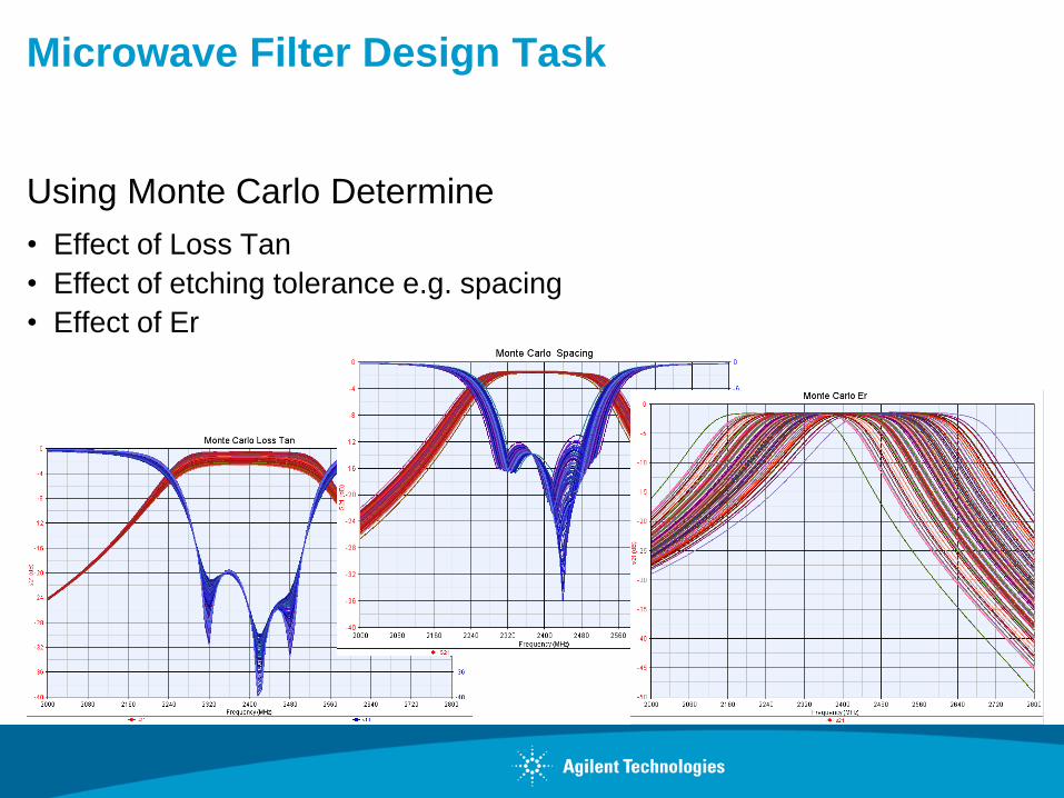
Microwave Filter Design Task
Using Monte Carlo Determine
• Effect of Loss Tan
• Effect of etching tolerance e.g. spacing
• Effect of Er
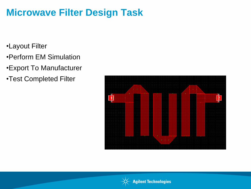
Microwave Filter Design Task
•Layout Filter
•Perform EM Simulation
•Export To Manufacturer
•Test Completed Filter

Microwave Filter Design Task
• Measure Filter
– TESTLINK
• Compare to Simulation
Measured
EM
Modeled

Microwave Filter Design Task
Performance Summary
Center Frequency 2450 MHz 2390 MHz
Bandwidth 200 MHz 260 MHz
Insertion Loss 2 dB 3.2 dB
$ Cost ? ~$0.50
Note: Know your substrate material especially ER and Loss Tan

Microwave Filter Design Task
Link data to SPECTRASYS’ behavioral model
Po=1.2 dB
NF=0.1dB

Microwave Filter Design Task
MFILTER- A better way
• Classical synthesis shapes
– Butterworth, Chebyshev, Elliptical etc.
• Multiple topologies
• Instant schematic and graphical updates
• Coupled or Tapped input
• Multiple physical realizations e.g. stripline, microstrip, inverted microstrip etc. via Advanced T-Line
– Automatic compensation of vias, grounds, steps, and T-Junctions
• Direct link to layout and EM simulation engine
• Monte Carlo, Yield and what If analysis
• Measurement of Device via TESTLINK

Lumped Filter Design Task
70 MHz IF Filter
• System Specifications / Goals
– Frequency- 60-80 MHz
– Insertion Loss- 0.5dB ?
– Shape- Butterworth
– Order- 14 ?

Lumped Filter Design Task
PASSIVE FILTER - A Better Way
• Start With Filter Type Shape
– Low-pass, High-pass, Band-pass, Band-reject
• Shape
– Butterworth, Chebyshev, Bessel, Elliptical etc.
• Subtype
– Eight physical formats
• Some Formats Lend Themselves Better to Wide or Narrow Responses
Note: Changes in schematic and graph when parameters are changed is Instantaneous

Which Shape And Subtype To Pick?
• Component Count
• Response BW, Group Delay
• Out Of Band Response
– Symmetry, Roll Off
• Ease of Manufacture
– Common Inductance or Capacitance
Balanced Circuit at a Buttons Click!
Lumped Filter Design Task

Multiple Filter Shapes
• Butterworth
• Chebyshev
• Bessel
• Singly Terminated
– For Diplexers etc.
Lumped Filter Design Task

Settings
• Input / Output Resistance
– Not limited to 50 ohms or symmetrical impedances!
• Cutoff Frequencies
• Filter Order
• Specify Cutoff Attenuation
• Common L or C for some filter types
Lumped Filter Design Task

Lumped Filter Design Task
Response of Synthesized Shunt C Coupled Filter
• Shunt C Coupled filter results in common inductor
– Five Sections Chosen

Lumped Filter Design Task
Using Standard Values Results in Shifted Response
• Tune Standard Values for best results
Original vs. standard values

Lumped Filter Design Task
Replacing Ideal Std Values with Manufacturers S-data
• Increased insertion loss due to finite Q’s of components
• Be Mindful of SRF and Qs of Manufacturer’s Components and The Frequency range of their data
Original vs. S-data values
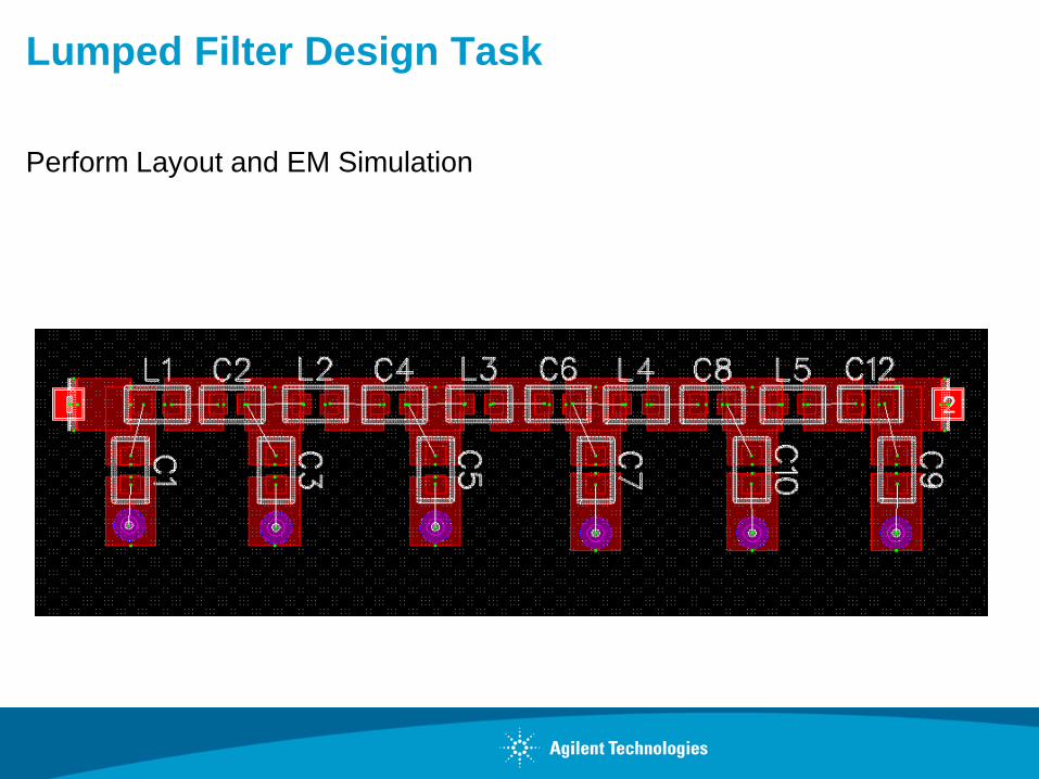
Lumped Filter Design Task
Perform Layout and EM Simulation

Lumped Filter Design Task
EM simulation with S-Data Parts
Use Co-Simulation to Fine Tune Standard Valued S-Data
• Only a single EM simulation is required
since copper pattern is invariant
Filter with S-data specified parts
EM Filter with S-data specified parts

Lumped Filter Design Task
Comparison of Original Synthesized Filter
Use Monte Carlo for Yield and Manufacturability

Lumped Filter Design Task
Pad and Dielectric Effects
• More prominent at higher frequencies, 500MHz Filter example shown
Er= 3.9, 4.5, 4.9
H=10mil
H=30mil
H=59mil
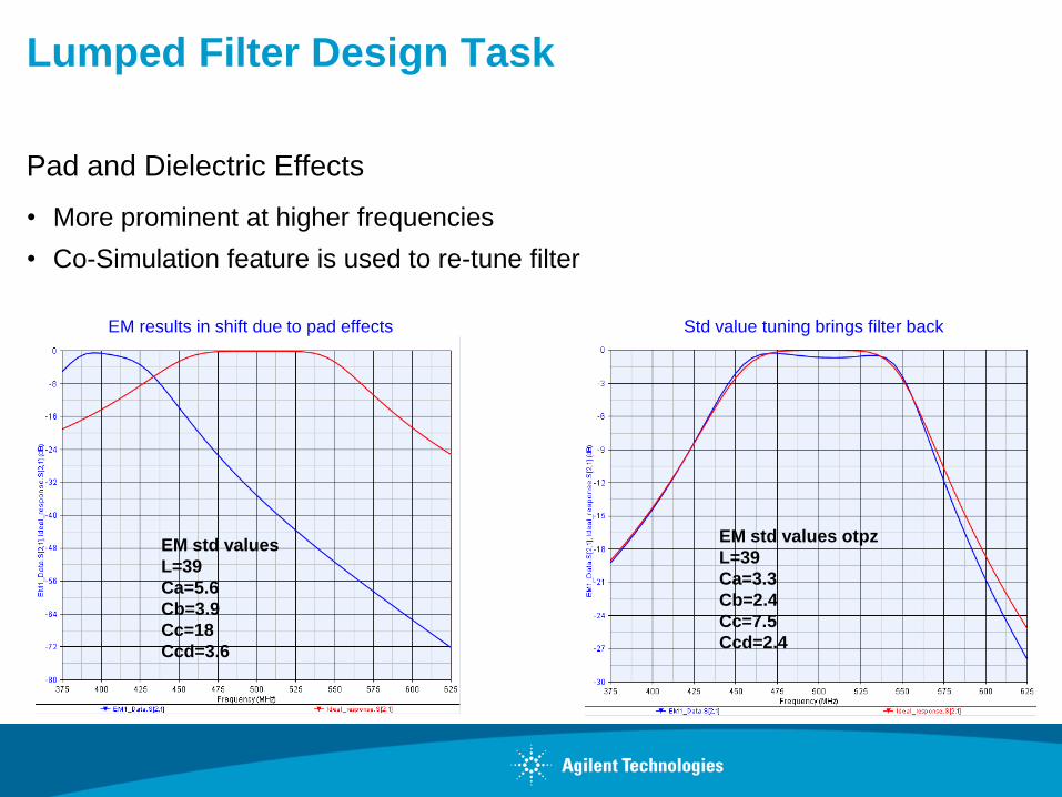
Lumped Filter Design Task
Pad and Dielectric Effects
• More prominent at higher frequencies
• Co-Simulation feature is used to re-tune filter
EM std values
L=39
Ca=5.6
Cb=3.9
Cc=18
Ccd=3.6
EM std values otpz
L=39
Ca=3.3
Cb=2.4
Cc=7.5
Ccd=2.4
EM results in shift due to pad effects Std value tuning brings filter back

Lumped Filter Design Task
Performance Summary
Center Frequency 70 MHz
68.1 Std Pts
67 MHz
Bandwidth 20 MHz
17.3 Std Pts
17 MHz
Sections 14 5
Insertion Loss 0.5 dB 3.9 dB
$ Cost ? ~$2.90 (16x$0.15)
Note: Know your substrate material especially ER and LossTan

Lumped Filter Design Task
Link data to SPECTRASYS’ behavioral model
• When S-Parameter File is Substituted For Behavioral Model In System Simulator
– Note: 3db Additional Loss And Increase In Spur Level (below noise floor) And An
Increase Of 0.11dB In Noise Figure

Lumped Filter Design Task
PASSIVE FILTER- A better way
• Classical synthesis shapes
– Butterworth, Chebyshev, Bessel, Singly Terminated etc.
• Multiple topologies
• Instant schematic and graphical updates
• Single or Balance types
• Direct link to layout and EM simulation engine
– Co-Simulation aides final optimization
• Monte Carlo and Yield analysis
• Measurement of Device via TESTLINK

Signal Control Design Task
What is Signal Control?
• Distribution And Control Of Power Through The Use Of
– Couplers, Splitters, Dividers, Attenuators, Baluns
• Where Is It Used?
– Power Monitoring, Amplifiers, Mixers, Power Combining, Beam Forming

Signal Control Design Task
Signal Control Elements
• Splitters
– Single or Multi-section, 0 deg, 180 deg
• Couplers
– Lange, Backward Wave, Lumped
• Power Dividers
– Distributed, Lumped
• Balun
• Attenuators

Signal Control Design Task
SIGNAL CONTROL, a better way!
• Topology
– Selection of over 43 topologies
• Splitters
• Couplers
• Power Dividers
• Baluns
• Attenuators
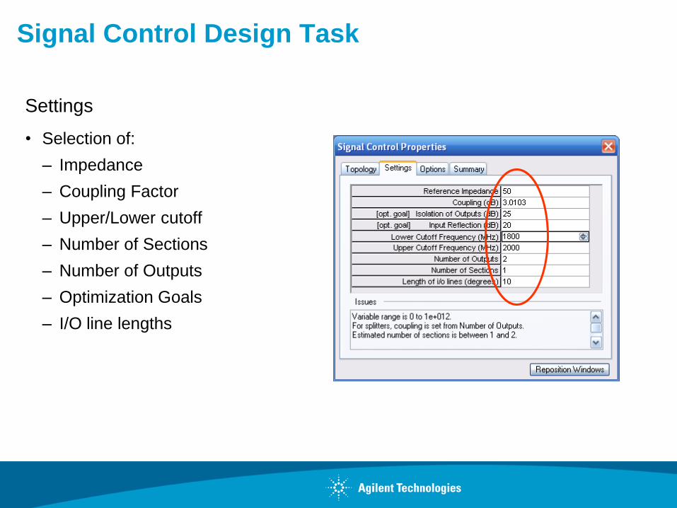
Signal Control Design Task
Settings
• Selection of:
– Impedance
– Coupling Factor
– Upper/Lower cutoff
– Number of Sections
– Number of Outputs
– Optimization Goals
– I/O line lengths

Signal Control Design Task
Instant Realization
• Dynamic Schematic and Graphs

Signal Control Design Task
Options
• Create a Layout
• Use Advanced TLINE to Convert to Physical Format

Signal Control Design Task
Options
• Manufacturing Process
– Select Physical Form
• Switch between any of the
processes (e.g. ideal to
microstrip, stripline to microstrip
etc.)
– Accounts for discontinuities,
corners, steps etc.
– Uses selectable substrate
definition

Signal Control Design Task
Conversion to Microstrip Causes Shift
• Shift due to non-ideal models, losses, dispersion etc.
– Re-optimize element parameters to specifications
Shift due to Microstrip

Signal Control Design Task
Layout Is Created By Checking Box in Options Tab
EM Simulation Is Performed To Verify Design Goals

Signal Control Design Task
EM Simulation Shows Difference In Isolation Between Output Ports
EMPOWER’s Ability To Co-Simulate Allows The Tuning Of Isolation
Resistor For Optimum Isolation
Optimum R= 91 ohms instead of 100 ohms

Signal Control Design Task
SIGNAL CONTROL- A better way
• Over 43 Topologies
– Splitters, Couplers, Baluns, Attenuators
• 0 deg, 90 deg, 180 deg types
– Multiple outputs, Multiple stages
• Instant schematic and graphical updates
• Optimization of final process
• Direct link to layout and EM simulation engine
– Co-Simulation aides final optimization
• Monte Carlo and Yield analysis
• Measurement of Device via TESTLINK
• Link data to SPECTRASYS’ behavioral model

Matching Design Task
Where is Matching used?
• At Almost Every Interface Between Connected Components
– Minimize Power Loss Between Entities

Matching Design Task
Front End Receiver Amp Parameters
• Frequency Range 2200 MHz to 2600 MHz
• Gain 30dB
• Noise Figure 3dB
• Match Nominal 50 Ohm Input/Output
• P1dB +10dBm
• PSAT 13dBm
• TOI 20dBm

Matching Design Task
Complex Matching Issues
• Simultaneous Matching For Noise Figure, Input/Output, and Interstage
– Difficult Using Manual Techniques, Especially For Conditionally Stable Device
Selected Part Meets Our Gain And Noise Figure Needs
NE52418

Matching Design Task
Conditionally Stable
• Simultaneous Input/Output Match Is Not Possible
• Good News, Noise Figure Meets Our Goal With 50 Ohm Input
Matching Design Task
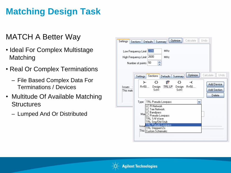
MATCH A Better Way
• Ideal For Complex Multistage
Matching
• Real Or Complex Terminations
– File Based Complex Data For
Terminations / Devices
• Multitude Of Available Matching
Structures
– Lumped And Or Distributed

Matching Design Task
Nominal Goals Met With Interstage Matching Sections

Matching Design Task
Matching Network Incorporated Into Design
• Use Advance TLINE
– Converts To Physical Process
• Includes Steps, Discontinuities, Vias, etc.

Matching Design Task
Monte Carlo Analysis
•Matching <100% Yield, Determine Effect On System Or End User
•Gain And NF 100% Yield

Matching Design Task
Optimize Circuit For Response And Match
•Measure Pertinent Parameters
– Frequency Range 2.2 GHz-2.6 GHz
Gain 30dB +/- .5 dB
Noise Figure 1.06 dB
Match <-15dB
? P1dB 0 dBm (10 dBm)
? TOI 18.6 dBm (20 dBm)
? PSAT 10.4 dBm (13 dBm)

Matching Design Task
Replacing Behavioral Model With Design
•No Significant Change In Spur Or Harmonic Content
•Noise Figure Improved by 2dB
Matching Design Task
MATCH- A better way
• Multiple matching networks and topologies
– Mix and match between distributed and lumped networks
• Match to real, complex and S/Y/Z files
– Broadband matching, Multi-stage matching
• Instant schematic and graphical updates
• Direct link to layout and EM simulation engine
– Co-Simulation aides final optimization
• Monte Carlo and Yield analysis
• Link Data To SPECTRASYS’ Behavioral Model

Summary
Reviewed Of Common Design Tasks
Reviewed Non-Synthesis Methods
Showed A Better Way To Solve Complex Design Challenges
• Synthesis
• Incorporating Standard Values
– Substituted Measured S-Data For Accuracy
– Optimized Performance
• Layout And EM Simulation For Verification
• Exported Data For Incorporation Into Higher Level Design
We Showed A Comprehensive Set Of Tools, In a Common Environment For Rapid Development, Improving Time To Market With Fewer Re-Designs

More GENESYS Web Resources
Agilent GENESYS home page
http://www.eagleware.com
Product & Apps questions? Ask!
http://www.eagleware.com/contact.html
Video product demonstrations
http://www.eagleware.com/apps/eagleware_demos.html
Agilent GENESYS discussion Forums
http://www.agilent.com/find/eesof-ewforum
Receive our monthly email newsletter containing the latest
application information & product tips.
http://eesof.tm.agilent.com/forms/visitor.html


![RF Circuit Design - Chris Bowick[1]](https://static.fdocuments.us/doc/165x107/547fc956b4af9f943f8b4573/rf-circuit-design-chris-bowick1.jpg)
![RF circuits design 6ue.pwr.wroc.pl/.../lecture/RF_circuits_design_6.pdfAmplifier block diagram RF transistor [S] Output matching circuit Input matching circuit BIAS circuit ZG ZL Amplifier](https://static.fdocuments.us/doc/165x107/5e41026cfd4507719c31d8c5/rf-circuits-design-6uepwrwrocpllecturerfcircuitsdesign6pdf-amplifier.jpg)