RF Circuit Design Vidyalankarvidyalankar.org/file/engg_degree/prelim_paper_soln/SemV/EXTC/RFC.pdfA...
17
1013/Engg/TE/Pre Pap/2013/EXTC/Soln/RFC 1 Vidyalankar T.E. Sem. V [EXTC] RF Circuit Design Prelim Question Paper Solution Chip Resistors The size of chip resistors can be as small as 40 by 20 mils (where 1 mil = 0.001 inch = 0.0254 mm) for 0.5 W power ratings and up to 1 by 1 inch for 1000 W ratings in RF power amplifiers. The chip resistors sizes that are most commonly used in circuits operating up to several hundered watts are summarized in Table. 1. A general rule of thumb in determining the size of the chip components from the known size code is as follows: the first two digits in the code denote the length L in terms of tens of mils, and the last two digits denote the width W of the component. The thickeness of the chip resistors is not standardized and depends on the particular component type. The resistance value range from 1/10 up to several M. Higher values are difficult to manufacture and result in high tolerances. Typical resistor tolerance values range from 5% to 0.1%. Another difficulty that arises with high-value resistors is that they are prone to produce parasitic fields, adversely affecting the linearity of the resistance versus frequency behaviour. A conventional chip resistor realization is shown in figure 1. Table 1 : Standard sizes of chip resistors Geometry Size Code Length L, mills Width W, mils 0402 40 20 0603 60 30 0805 80 50 1206 120 60 1218 120 180 A metal film (usually nichrome) layer is deposited on a ceramic body (usually aluminum oxide). This resistive layer is trimmed to the desired nominal value by reducing its length and inserting inner electrodes. Contacts are made on both ends of the resistor that allow the component to be soldered to the board. The resistive film is coated with a protective layer to prevent environment interfereneces. Given : N D = 10 16 cm 3 , d = 0.75 m, W = 10 m, L = 2m, r = 12.0, V d = 0.8V, n = 8500 cm 2 /(Vs). 1. (a) 1. (b) Fig. 1: Cross-sectional view of a typical chip resistor Vidyalankar
Transcript of RF Circuit Design Vidyalankarvidyalankar.org/file/engg_degree/prelim_paper_soln/SemV/EXTC/RFC.pdfA...

1013/Engg/TE/Pre Pap/2013/EXTC/Soln/RFC 1
Vidyalankar T.E. Sem. V [EXTC] RF Circuit Design
Prelim Question Paper Solution
Chip Resistors The size of chip resistors can be as small as 40 by 20 mils (where 1 mil = 0.001 inch = 0.0254 mm) for 0.5 W power ratings and up to 1 by 1 inch for 1000 W ratings in RF power amplifiers. The chip resistors sizes that are most commonly used in circuits operating up to several hundered watts are summarized in Table. 1. A general rule of thumb in determining the size of the chip components from the known size code is as follows: the first two digits in the code denote the length L in terms of tens of mils, and the last two digits denote the width W of the component. The thickeness of the chip resistors is not standardized and depends on the particular component type. The resistance value range from 1/10 up to several M. Higher values are difficult to manufacture and result in high tolerances. Typical resistor tolerance values range from 5% to 0.1%. Another difficulty that arises with high-value resistors is that they are prone to produce parasitic fields, adversely affecting the linearity of the resistance versus frequency behaviour. A conventional chip resistor realization is shown in figure 1. Table 1 : Standard sizes of chip resistors
Geometry Size Code Length L, mills Width W, mils 0402 40 20
0603 60 30 0805 80 50 1206 120 60 1218 120 180
A metal film (usually nichrome) layer is deposited on a ceramic body (usually aluminum oxide). This resistive layer is trimmed to the desired nominal value by reducing its length and inserting inner electrodes. Contacts are made on both ends of the resistor that allow the component to be soldered to the board. The resistive film is coated with a protective layer to prevent environment interfereneces.
Given : ND = 1016 cm3, d = 0.75 m, W = 10 m, L = 2m, r = 12.0, Vd = 0.8V, n = 8500 cm2/(Vs).
1. (a)
1. (b)
Fig. 1: Cross-sectional view of a typical chip resistor Vidyala
nkar
Vidyalankar : T.E. − RFC
1013/Engg/TE/Pre Pap/2013/EXTC/Soln/RFC 2
Pinch off voltage
VP = 2
dq.N d
2
= 219 16 6 3
0 r
1.6 10 10 10 m 0.75
2
=
10
12
9 10
2 8.85 10 12
VP = 4.23 V Vd = 0.8 V
VTO = Vd Vp
= 3.44 V The saturation drain current is independent of the applied drain source voltage and is given by
IDSS = G03/2P
d dP
V 2V V
3 3 V
Here, G0 = qNDWd/L = q2nN
2DWD/L
= 8.16 S Substituting G0 and other values IDSS = 6.89 A
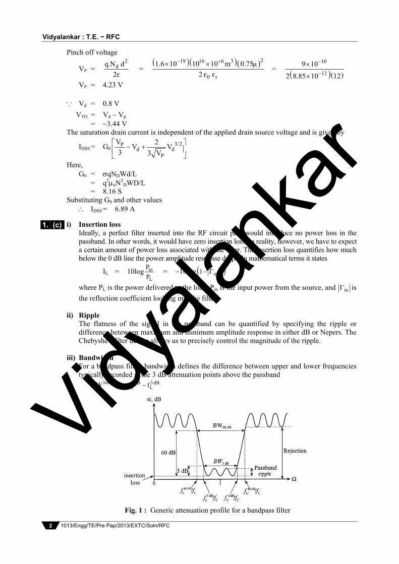
i) Insertion loss Ideally, a perfect filter inserted into the RF circuit path would introduce no power loss in the
passband. In other words, it would have zero insertion loss. In reality, however, we have to expect a certain amount of power loss associated with the filter. The insertion loss quantifies how much below the 0 dB line the power amplitude response drops. In mathematical terms it states
IL = 10log in
L
P
P = 10log 2
in1
where PL is the power delivered to the load, Pin is the input power from the source, and in is
the reflection coefficient looking into the filter. ii) Ripple The flatness of the signal in the passband can be quantified by specifying the ripple or
difference beteween maximum and minimum amplitude response in either dB or Nepers. The Chebyshev filter design allows us to precisely control the magnitude of the ripple.
iii) Bandwidth For a bandpass filter, bandwidth defines the difference between upper and lower frequencies
typically recorded at the 3 dB attenuation points above the passband
BW3dB = 3 dB 3 dBu Lf f
1. (c)
Fig. 1 : Generic attenuation profile for a bandpass filter
Vidyala
nkar

Prelim Question Paper Solution
1013/Engg/TE/Pre Pap/2013/EXTC/Soln/RFC 3
The Energy-band diagram for Schottky
Filter Implementation Filter designs beyond 500 MHz are difficult to realize with discrete components because the wavelengh becomes comparable with the physical filter element dimensions, resulting in various losses severely degrading the circuit performance. Thus, to arrive at practical filters, the lumped component filters must be converted into distributed element realizations.
To accomplish the conversion between lumped and distributed circuit designs, Richards proposed a special transformation that allows open-and short-circuit transmission line segments to emulate the inductive and capactive behaviour of the discrete components. The input impedence Zin of a short-circuit transmission line (ZL = 0) of characteristics line impedance Z0 is purely reactive: Zin = jZ0 tan(l) = jZ0 tan … (1)
Here, the electric length can be rewritten in such a way as to make the frequency behavior explicit.
= 0
8
= p
p 0
v2 f
v 8f
=
0
f
4 f
= 4
… (2)
By substituting (2) into (1), a direct link between the frequency-dependent inductive behavior of the transmission line and the lumped element representation can be established:
jXL = jL jZ0 tan0
f
4 f
= jZ0 tan4
= SZ0 … (3)
where S = j tan( / 4) is the actual Richards transform. The capacitive lumped element effect can be replicated through the open-circuit transmission line section.
jBC = jC jY0 tan4
= SY0 … (4)
Thus, Richards transformation allows us to replace lumped inductors with short-circuit stubs of characteristics impedance Z0 = L and capacitors with open-circuit stubs of characteristic impedance Z0 = 1 / C.
The normalized load impedances and corresponding reflection coefficients, return loss, and SWR values are computed as follows :
a) zL = 1, G = (zL 1) / (zL + 1) = 0, RKdB = , SWR = 1
b) zL = 0.97, G = (zL 1) / (zL + 1) = 0.015, RLdB = 36.3, SWR = 1.03
c) zL = 1.5 + j0.5, G = (zL 1) / (zL + 1) = 0.23 + j0.15, RLdB = 11.1, SWR = 1.77
d) zL = 0.2 j0.1, G = (zL 1) / (zL + 1) = 0.66 j0.14, RLdB = 3.5, SWR = 5.05
1. (d)
2. (a)
2. (b)
(a) Metal and semiconductor do not interact (b) Metal-semiconductor contact
Fig. 1 : Energy-band diagram of Schottky contact, (a) before and (b) after contact
Vidyala
nkar

Vidyalankar : T.E. − RFC
1013/Engg/TE/Pre Pap/2013/EXTC/Soln/RFC 4
To determine the approximate values of the SWR requires us to exploit the similarity with the input impedance. We first plot the normalized impedance values in the Smith Chart (see figure 1). Then we draw circles with centers at the origin and radii whose lengths reach the respective impedance points defined in the previous step. From these circles we see that the load refection coefficient for zero load reactance (xL = 0) is
G0 = L
L
z 1
z 1
= L
L
r 1
r 1
= Gr
The SWR can be defined in term of the real load reflection coefficient along the real G axis.
SWR = 0
0
1
1
= r
r
1
1
This requires | G0 | = Gr ≥ 0. In other words, for Gr ≥ 0 we have to enforce rL ≥ 1, meaning that
only intersects of the right-hand-side circles with the real axis define the SWR. Circuit Parameters for a Parallel Plate Transmission Line
3. (a)
Fig. 1 : SWR circles for various reflection coefficients
Fig. 1 : Parallel-plate transmission line geometry. The plate width w is large compared with the separation d.
Vidyala
nkar

Prelim Question Paper Solution
1013/Engg/TE/Pre Pap/2013/EXTC/Soln/RFC 5
Here we make following assumption : i) Plate width w is large compared with the plate separation d for a one-dimensional analysis to
apply. ii) We assume that the skin depth is small compared to the thickness dp of the plates to
simplify the derivation of the paramters. Under these conditions we are able to cast the electric and magnetic fields in the conducting plates in the form.
E = j tzzE x, z e … (1a)
H = j tyyH x, z e … (1b)
The term ejt represents the time dependence of the sinusoidal electric and magnetic fields, and phasors Ez(x, z) and Hy(x, z) encode spatial variations. We do not have any field dependency upon y, because the plates are assumed very wide, and thus the electromagnetic fields do not change appreciably along the y-axis. Application of the differential forms of Faraday’s and Ampere’s laws
E = t
… (2)
H = condE … (3) results in two differential equations
z
0z y
0
0 0z x
E0
y x
= zE
x
= y
0d
Hdt
0
= ydH
dt = jHy … (4)
and
y
0z y
0
0 Hz x
00
y x
= yH
x
= cound
z
0
0
E
= condEz … (5)
By differentiating (5) with respect to x and substituting (4), we find
2
y2
d H
dx = jcondHy = p2Hy … (6)
where p2 = jcond. The general solution for this second-order ordinary differential equation (6) is Hy(x) = Aepx + Bepx. The coefficients A and B are integration constants. We can now perform the following manipulations :
P = condj = condj = (1 + j) cond / 2 = (1 + j) / … (7)
where = cond2 / is recognized as the skin depth. Since p has a positive real component,
constant A should be equal to zero to satisfy the condition that the magnetic field in the lower plate must decay in amplitude for negative x. A similar argument can be made for the upper plate by setting B = 0. Thus, for the magnetic field in the lower conducting plate we have a simple exponential solution Hy = H0e
px = H0e(1 + j)x / … (8)
where B = H0 is a yet to be determined constant factor. Since the current density can be written as
jz = Ez = yH
x
=
1 j x/01 j He
… (9)
Vidyala
nkar

Vidyalankar : T.E. − RFC
1013/Engg/TE/Pre Pap/2013/EXTC/Soln/RFC 6
we are now able to relate the current density Jz to the total current flow I in the lower plate
I = zs
J dxdy = p
0
zd
w J dx =
p
01 j x /
0 dwH e
= p1 j d /0wH 1 e
… (10)
where S is the cross sectional area of the lower plate and dp is the thickness of that plate. Since we assume that dp » , the exponential term in (10) drops out and I = H0. From this we conclude that H0 = I / w. The electric field at the surface of the conductor (x = 0) can be specified as
Ez (0) = z
cond
J 0
=
0
cond
1 j H
= cond
1 j I
w
… (11)
Equation (11) allows us to compute the surface impedance per unit length, Zs, by eliminating the current I as follows:
Zs = Ez / I = cond cond
1 j
w w
= Rs + jLs … (12)
The surface resistance and surface inductance per unit length are then identified as
Rs = cond
1
w … (13)
Ls = cond
1
w … (14)
Both are dependent on the skin depth . It is important to point out that (13) and (14) apply for a single conductor. Since we have two conductors in our system (upper and lower plates) the total series resistance and inductance per unit length will be twice the value of Rs and Ls, respectively. To obtain the inductive and capacitive behavior of the mutual line coupling, we must employ the definitions of capacitance and inductance:
C = Q
V =
D.dS
V =
x
x x
E dS
E dl = x
x
w
E d
=
w
d
C =
w
d
… (15)
and
L = B.dS
I =
yH dS
i
= yH d
I
= y
y
H d
H w
=
d
w
L =
d
W
… (16)
where we have used the result of (10) to compute the current I = wHy Both in (15) and (16) the capacitance and inductance are given per unit length. Finally, we can express the conductance G in a similar way as derived in (15) :
G = J.dS
V =
diel x
x
E dS
E dl
= diel x
x
E w
E d
= dielw
d
G = diel w
d
… (17)
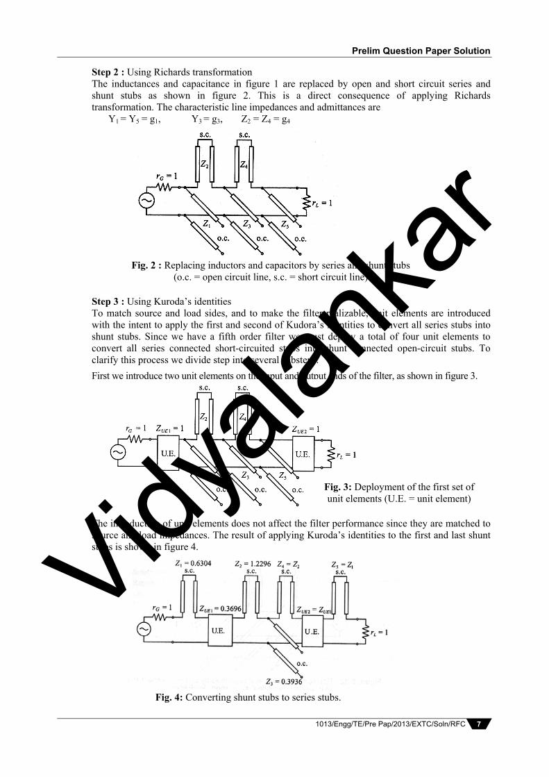
Step 1 : Consider a filter of order N = 5 with coefficients. g1 = 1.7058 = g5, g2 = 1.2296 = g4, g3 = 2.5408, g6 = 1.0 The normalized low-pass filter is given in figure 1.
3. (b)
Fig. 1 : Normalized low-pass filter of order N = 5
Vidyala
nkar
Prelim Question Paper Solution
1013/Engg/TE/Pre Pap/2013/EXTC/Soln/RFC 7
Step 2 : Using Richards transformation The inductances and capacitance in figure 1 are replaced by open and short circuit series and shunt stubs as shown in figure 2. This is a direct consequence of applying Richards transformation. The characteristic line impedances and admittances are Y1 = Y5 = g1, Y3 = g3, Z2 = Z4 = g4
Step 3 : Using Kuroda’s identities To match source and load sides, and to make the filter realizable, unit elements are introduced with the intent to apply the first and second of Kudora’s identities to convert all series stubs into shunt stubs. Since we have a fifth order filter we must deploy a total of four unit elements to convert all series connected short-circuited stubs into shunt connected open-circuit stubs. To clarify this process we divide step into several substeps.
First we introduce two unit elements on the input and output ends of the filter, as shown in figure 3.
The introduction of unit elements does not affect the filter performance since they are matched to source and load impedances. The result of applying Kuroda’s identities to the first and last shunt stubs is shown in figure 4.
Fig. 2 : Replacing inductors and capacitors by series and shunt stubs (o.c. = open circuit line, s.c. = short circuit line)
Fig. 3: Deployment of the first set of unit elements (U.E. = unit element)
Fig. 4: Converting shunt stubs to series stubs.
Vidyala
nkar

Vidyalankar : T.E. − RFC
1013/Engg/TE/Pre Pap/2013/EXTC/Soln/RFC 8
This version of the circuit is still nonrealizable because we have four series stubs. To convert them to shunt connections, we have to deploy two more unit elements, as shown in figure 5. Again, the introduction of unit elements does not affect the performance of the filter since they are matched to the source and load impedances. Applying Kuroda’s identities to the circuit shown in figure 5, we finally arrive at the realizable filter design, depicted in figure 6. Step 4 : Denormalization De-normalization involves scaling the unit elements to the 50 input and output impedances and computing the length of the lines based. Using vp = 0.6c = 1.8 108 m/s, the length is found to be l = (0 / 8) = vp / (8f0) = 7.5 mm. The final design implemented in microstrip lines is shown in figure 6(a). Figure 6(b) plots the attenuation profile in the frequency range 0 to 3.5 GHz. We notice that the passband ripple does not exceed 0.5 dB up to the cut-off frequency of 3 GHz. The second design project involves a more complicated bandstop filter, which requires the transformation of the low-pass prototype with a unity cut-off frequency into a design with specified center frequency and lower and upper 3 dB frequency points.
Fig. 5 : Deployment of the second set of unit elements to the fifth-order filter.
Fig. 6 : Realizable filter circuit obtained by converting series and shunt stubs using Kuroda’s identities.
Vidyala
nkar

Prelim Question Paper Solution
1013/Engg/TE/Pre Pap/2013/EXTC/Soln/RFC 9
The drain current flow in HEMT is the narrow interface between the GaAlAs and the GaAs layer. Hence, consider the energy band diagram of GaAlAs GaAs interface below.
2
2
d V
dx = D
H
qN
… (1)
The boundary conditions for the potential are imposed such that V(x = 0) = 0 and at the metal-semiconductor side V(x = d) = Vb + VG + WC / q. Here Vb is the barrier voltage, WC is the energy difference in the conduction levels between the n-doped GaAlAs and GaAs; and VG is comprised of the gate-source voltage as well as the channel voltage drop VG = VGS + V(y). To find the potential V, (1) is integrated twice. At the metal-semiconductor we set
V(d) = 2Dy
H
qNx E 0 d
2
… (2)
which yields
E(0) = GS T01
V V y Vd
… (3)
The HEMT threshold voltage VT0 as VT0 = Vb WC/q VP. Here we have used the previously defined pinch-off voltage VP = qNDd2 / (2H). From the known electric filed at the interface, we find the electron drain current
ID = EyA = qnNDEWd = qnNDdv
dy
Wd … (4)
The current flow is restricted to a very thin layer so that it is appropriate to carru out the integration over a surface charge density QS at x = 0. The result is = nQ / (WLd) = nQS / d. For the surface charge density we find with Gauss’s law QS = HE(0). Inserted in (5), we obtain
L
D0
I dy = DSV
n S0
W Q dV … (5a)
Upon using (3), it is seen that the drain current can be found
IDL = nW DSV
HGS T0
0
V V V dVd
… (5b)
or ID = n 2
DSHDS GS T0
VWV V V
Ld 2
… (5c)
Pinch-off occurs when the drain-source voltage is equal to or less than the differnce of gate-source and threshold voltages (i.e. VDS VGS VT0). If the equality of this condition is substituted in (7c), it is seen
ID = 2Hn Gs T0
WV V
2Ld
… (6)
4. (a)
Fig. 1 : Energy band diagram of GaAlAs-GaAs interface for an HEMT
Vidyala
nkar

Vidyalankar : T.E. − RFC
1013/Engg/TE/Pre Pap/2013/EXTC/Soln/RFC 10
Taking w
h 2, we have
A = 0 r r
f r r
Z 1 1 0.112 0.23
Z 2 1
= 1.5583
Substituting this result below.
w
h =
A
2A
8e
e 2 = 1.8477
Then, effective dielectric constant to be
eff = 1/2
r r1 1 h1 12
2 2 w
= 3.4575
We can compute the chartacteristic impedance of the line to verify our result
Z0 = f
eff
Z
w 2 w1.393 ln 1.444
h 3 h
= 50.2243 which is very close to the target impedance of 50 and therefore indicates that our result is correct. Using the obtained ratio for w/h, we find the trace width to be w = 73.9 mil. Finally, the effective dielectric constant just computed allows us to evaluate the phase velocity of the microstrip line vp = c/ eff = 1.61 108 m/s at f = 2GHz
and the effective wave length at 2 GHz = vp / f = 80.67 mm
Small-Signal BJT Models A small-signal hybrid BJT model is shown below. To make the model more realistic, a resistor r is connected in shunt to the feedback capacitor C. For this model we can directly establish the small-circuit parameters by expanding the input voltage VBE and output current IC about the biasing or Q-point in terms of small AC voltage vbe and current ic as follows:
VBE = QbeBEV v … (1a)
IC = QcCI i = ISexp Q
be TBEV v / V = 2
Q be beC
T T
v v1I 1 ...
V 2 V
… (1b)
4. (b)
5. (a)
Fig. 1 : Small-signal hybrid- Ebers-Moll BJT model. Vidyala
nkar

Prelim Question Paper Solution
1013/Engg/TE/Pre Pap/2013/EXTC/Soln/RFC 11
Truncating the sereies expansion of the exponential expression after the linear term, we find for all the small-signal collector current
ic = QC
beT
Iv
V
= gm vbe … (2)
where we identify the transconductance
gm = C
BE Q
dI
dV = BE T
QV /V C
SBE TQ
IdI e
dV V … (3)
and the small-signal current gain at the operating point
F Q = C
B Q
dI
dI = 0 … (4)
The input resistance is determined through the chain rule:
r = BE
B Q
dV
dI = C BE
B CQ Q
dI dV
dI dI = 0
mg
… (5)
For the output conductance we have
0
1
r = C
CE Q
dI
dV = BE T
QV /V CE C
sCE AN ANQ
IVdI e 1
dV V V
… (6)
which includes the Early effect, also known as the base-width modulation because of the increased depletion layer extend into the base. It is directly seen that this model in its simplest form at the terminals B -C-E reduces for the static case and, under negligence of the collector-emitter resistance, to our familiar low-frequency transistor model. Here the output can simply be expressed in term of the input voltage vbe as
ic = bem be
vg v
r = (1 + gm) bev
r = (1 + 0) bev
r … (7)
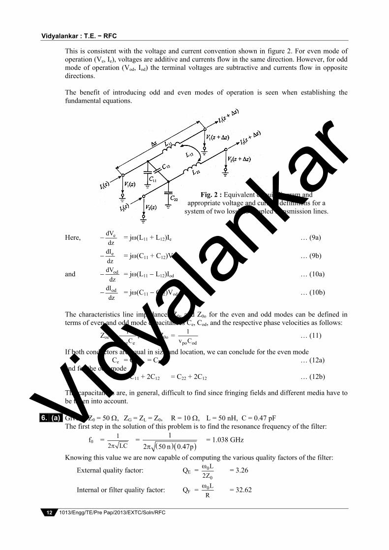
Coupled filter The configuration consist of two lines separated over a distance S and attached to a dielectric medium of thickness d and dielectric constant r. The strip lines are W wide, and the thickness is negligible when compared with d. The capacitance and inductive coupling phenomena between the lines and ground is schematically given in figure 1. Here equal indices denote self-capacitances and inductances, whereas index 12 stands for coupling between line 1 and line 2 (which is equal to coupling between line 2 and line 1).
We can now define an even mode voltage Ve and current Ie and an odd mode voltage Vod and current Iod in terms of the total voltages and currents at terminals 1 and 2 such that
Ve = 1 21
V V2
, Ie = 1 21
I I2
… (8a)
and Vod = 1 21
V V2
, Iod = 1 21
I I2
… (8b)
5. (b)
Fig. 1 : Coupled microstrip lines. Vidyala
nkar
Vidyalankar : T.E. − RFC
1013/Engg/TE/Pre Pap/2013/EXTC/Soln/RFC 12
This is consistent with the voltage and current convention shown in figure 2. For even mode of operation (Ve, Ie), voltages are additive and currents flow in the same direction. However, for odd mode of operation (Vod, Iod) the terminal voltages are subtractive and currents flow in opposite directions. The benefit of introducing odd and even modes of operation is seen when establishing the fundamental equations.
Here, edV
dz = j(L11 + L12)Ie … (9a)
edI
dz = j(C11 + C12)Ve … (9b)
and oddV
dz = j(L11 L12)Iod … (10a)
oddI
dz = j(C11 C12)Vod … (10b)
The characteristics line impedances Z0e and Z0o for the even and odd modes can be defined in terms of even and odd mode capacitances Ce, Cod, and the respective phase velocities as follows:
Zoe = pe e
1
v C, Z0o =
po od
1
v C … (11)
If both conductors are equal in size and location, we can conclude for the even mode Ce = C11 = C22 … (12a) and for the odd mode Cod = C11 + 2C12 = C22 + 2C12 … (12b)
The capacitances are, in general, difficult to find since fringing fields and different media have to be taken into account.
Given : Z0 = 50 , ZG = ZL = Z0, R = 10 , L = 50 nH, C = 0.47 pF The first step in the solution of this problem is to find the resonance frequency of the filter:
f0 = 1
2 LC =
1
2 50 n 0.47p = 1.038 GHz
Knowing this value we are now capable of computing the various quality factors of the filter:
External quality factor: QE = 0
0
L
2Z
= 3.26
Internal or filter quality factor: QF = 0L
R
= 32.62
6. (a)
Fig. 2 : Equivalent circuit diagram and appropriate voltage and current definitions for a
system of two lossless coupled transmission lines.
Vidyala
nkar

Prelim Question Paper Solution
1013/Engg/TE/Pre Pap/2013/EXTC/Soln/RFC 13
Loaded quality factor QLD = 0
0
L
R 2Z
= 2.97
To determine the input power, or maximum available power from the source, we use
Pin = 2G 0V / 8Z = 62.5 mW
Due to nonzero internal resistance of the filter (R = 10 ), the signal will suffer some attenuation even at the resonance frequency and the power delivered to the load will be less than the available power:
PL = Pin 0
2 2 2 2LD E LD f f
1
1 Q Q / Q
= Pin 2 2
E LD
1
Q / Q = 51.7 mW
LD
Q 3.26
Q 2.97
Significance of Quarter-Wave Transmission Line When Zin(d) ZL, load mismatch takes place which results in power losses at the load impedance, due to reflections. This severely degrades the performance of an RF System by setting d = / 2 (or more geneally
Zin(d = / 2) = Z0
L 0
0 L
2Z jZ tan .
22
Z jZ tan .2
= ZL … (1)
In other words, if the line is exactly a half wavelength long, the input impedance is equal to the load impedance, independent of the characteristic line impedance Z0.
As a next step, let us reduce the length to d = /4 (or d = /4 + m(/2), m = 1, 2, …). This yields
Zin(d = / 4) = L 0
0
0 L
2Z jZ tan .
4Z2
Z jZ tan .4
= 20
LZ
… (2)
The implication of (2) leads to the lambda-quarter transformer, which allows the matching of a real load impedance to a desired real input impedance by choosing a transmission line segment whose characteristic impedance can be computed as the geometric mean of load and input impedances: Z0 = L inZ Z … (3)
This is shown in figure 1, where Zin and ZL are known impedances and Z0 is determined based on (2). The idea of impedance matching has important practical design implications and is investigated. Chebyshev-Type Filters The design of an equi-ripple filter type is based on an insertion loss whose functional behaviour is described by the Chebyshev polynomials TN () in the following form: IL = 10log{LF} = 10log {1 + a2T2
N () … (1) where TN () = cos {N [cos1 ()]}, for || 1 TN () = cosh {N [cosh1 ()]}, for || ≥ 1
6. (b)
7. (a)
Fig. 1 : Input impedance matched to a load impedance through a /4 line segment Z0 Vidy
alank
ar

Vidyalankar : T.E. − RFC
1013/Engg/TE/Pre Pap/2013/EXTC/Soln/RFC 14
To appreciate the behaviour of the Chebyshev polynomials in the normalized frequency range 1 < < 1, we list the first five terms: T0 = 1, T1 = , T2 = 1 + 22, T3 = 3 + 43, T4 = 1 82 + 84 The functional behaviour of the two terms is a constant and a linear function, and the subsequent three terms are quadratic, cubic, and fourhorder functions, as seen in figure 3. It can be observed that all polynomials oscillate within a 1 interval, a fact that is exploited in the equi-ripple design. The magnitude of the transfer function |H(j)| is obtained from the Chebyshev polynomial as follows:
|H () | = *H H = 2 2
N
1
1 a T … (2)
where TN () is the Chebyshev polynomial of order N and a is a constant factor that allows us to control the height of the passband ripples. For instance, if we choose a = 1, then at = 1 we have
|H(0)| = 1
2 = 0.707
Operation of PN-Junction The physical contact of a p-type with an n-type semiconductor leads to one of the most important concepts when dealing with active semiconductor devices: the pn-junction. Because of the difference in the carrier concentrations between the two types of semiconductors a current flow will be initiated across the interface. This current is commonly known as a diffusion current and is composed of electrons and holes. We consider a one-dimensional model of the pn-junction as seen in figure 1.
7. (b)
Fig. 1 : Current flow in the pn-junction
Fig. 1 : Chebyshev polynomials T1 () through T4 () in the normalized frequency range 1 1.
Vidyala
nkar

Prelim Question Paper Solution
1013/Engg/TE/Pre Pap/2013/EXTC/Soln/RFC 15
The diffusion current is composed of diffnI and
diffpI components:
Idiff = diff diffn pI I = qA n p
dn dpD D
dx dx
… (1)
where A is the semiconductor cross-sectional area orthogonal to the x-axis, and Dn, Dp are the diffusion constants for electrons and holes in the form (Einstein relation)
Dn, p = n ,pkT
q = n, p VT … (2)
The thermal potential VT = kT / q is approximately 26 mV at room temperature of 300 K.
Since the p-type semiconductor was initially neutral, the diffusion current of holes is going to leave behind a negative space charge. Similarly, the electron current flow from the n-semiconductor will leave behind positive space charges. As the diffusion the n-semiconductor and the net negative charge in the p-semiconductor. This field in turn induces a current IF = AE which opposes the diffusion current such that IF + Idiff = 0. Substituting for the conductivity, we find IF = qA(nn + pp)E =
F Fn pI I … (3)
Since the total current is equal to zero, the electron portion of the current is also equal to zero; that is,
diff Fn nI I = qDnA
dn
dx+ qnnAE = qnnA T
dn dVV n
dx dx
= 0 … (4)
where the electric field E has been replaced by the derivative of the potential E = dV / dx. Integrating (4), we obtain the diffusion barrier voltage or, as it is often called, the built-in potential:
diffv
0
dV = Vdiff = n
p
n1
Tn
V n dn = VTln n
p
n
n
… (5)
where again nn is the electron concentration in the n-type and np is the electron concentration in the p-type semiconductor. The same diffusion barrier voltage could have been found had we considered the hole current flow from the p to the n-semiconductor and the corresponding balancing fieldinduced current flow IPF. The resulting equation describing the barrier voltage is
Vdiff = VTln p
n
p
p
… (6)
If the concentration of acceptors in the p-semiconductor is NA» ni and the concentration of donors
in the n-semiconductor is ND » ni, then nn = ND, np = 2i An / N , and by using (5) we obtain
Vdiff = VTln A D2i
N N
n
… (7)
Exactly the same result is obtained from (6) if we substitute pp = NA and pn = 2i Dn / N .
Kuroda’s Identities In addition to the unit element, it is important to be able to convert a practically difficult-to-implement design to a more suitable filter realization. For instance, a series inductance implemented by a short-circuit transmission line segment is more complicated to realize than shunt stub line. To facilitate the conversion between the various transmission line realizations, Kuroda has developed four identities which are summarized in table 1. In table 1 all inductances and capacitances are represented by their equivalent Richards transformations. As an example we will prove one of the identities and defer proof of the remaining identities to the problem.
7. (c) Vidyala
nkar

Vidyalankar : T.E. − RFC
1013/Engg/TE/Pre Pap/2013/EXTC/Soln/RFC 16
Table 1: Kuroda’s identities
Tunnel diode Tunnel diodes are pn-junction diodes that are made of n and p layers with extremely high doping (concentrations approach 1019 1020 cm3) that create very narrow space charge zones. The result is that the electrons and holes exceed the effective state concentrations in the conduction and valence bands. The Fermi level is shifted into the conduction band WCn of the n layer and into the valence band Wvp of the p+ semiconductor. We notice from figure 1 that the permissible electron states in either semiconductor layer are only separated through a very narrow potential barrier.
Based on quantum mechanical considerations, there is a finite probability that electrons can be exchanged across the narrow gap rather than having to overcome the potential barrier through an externally supplied voltage. This phenomenon is known as tunneling. In thermal equilibrium the electron tunneling from the n to p layer is balanced by the opposite tunneling from p to n layer. No let current flow results.
7. (d)
Fig. 1: Tunnel diode and its band energy representation. Vidy
alank
ar

Prelim Question Paper Solution
1013/Engg/TE/Pre Pap/2013/EXTC/Soln/RFC 17
The electric circuit of the tunnel diode. Here RS and LS are resistance of the semiconductor layers and associated lead inductance. The junction capacitance CT is in shunt with a negative conductance g = dI/dV, which is utilized in the negative slope of the I-V curve. A simplified amplifier circuit involving a tunnel diode is depicted in figure 3. If we consider the power amplification factor GT as the ratio of the power delivered to the load RL to the maximally
available power from the source PS = 2G GV / 8R , we obtain at resonance
TG = L
4
R =
2G L G
1
R 1/ R 1/ R g
where the influence of RS is neglected. If g is chosen appropriately (i.e., g = 1 / RL + 1 / RG), the denominator approaches zero and we have the behaviour of an oscillator.
Fig. 3 : Tunnel diode circuit for amplification/oscillation behavior
Fig. 2: Electric circuit representation of a tunnel diode.
Vidyala
nkar


![B.E. Sem. VII [EXTC] Fundamentals of Microwave …vidyalankar.org/file/engg_degree/prelim_paper_soln/SemVII/EXTC/... · Fundamentals of Microwave Engineering Prelim Question Paper](https://static.fdocuments.us/doc/165x107/5ab168727f8b9ad9788c3916/be-sem-vii-extc-fundamentals-of-microwave-of-microwave-engineering-prelim.jpg)