RF Channelizer Architectures using Iterative ...
4
RF Channelizer Architectures using Iterative Downconversion for Concurrent or Fast-Switching Spectrum Analysis (Invited Paper) Harish Krishnaswamy, Karthik Tripurari, Yang Xu, Linxiao Zhang, David Gidony, Branislav Jovanovic, Peter R. Kinget Dept. of Electrical Engineering, Columbia University, New York, NY 10027, USA Abstract—We propose an RF channelizer architecture that uses the concept of 3-way Iterative Down-Conversion (IDC) to channelize a wideband incident spectrum while only using a fixed LO synthesizer. The proposed architecture can realize a concurrent channelizer that can analyze channels simultaneously, or a fast-switching channelizer that can analyze channels sequentially but with very short switching times between channels. We present an RF channelizer demonstrator prototype that was fabricated in a 65nm CMOS process. It implements a partially-concurrent architecture with the ability to concurrently down-convert a subset of channels while being able to switch very quickly between the non-concurrent channels. It splits an input spectrum of 0.6GHz-9GHz into 7 channels each of 1.2GHz bandwidth. Channelizer performance depends on the selected operation mode. The measured channel switching duration can be as fast as 8ns, and is always under 1μs. The chip occupies an area of 2mm x 1mm and consumes an average power of 435mW while offering a dynamic range between 58dB to 63dB based on noise and linearity performance. I. I NTRODUCTION Future radio standards such as cognitive radio (CR) require broadband low-energy spectrum/signal analysis. Direct time-domain sampling and digitization over a multi- GHz bandwidth for digital signal analysis with multiple incident blockers necessitates a high-speed, high-dynamic- range, and consequently power-hungry, ADC. Frequency channelization can alleviate the energy requirement for spectrum analysis, as it relaxes the sampling rate and dynamic range requirements of the ADCs that follow due to the filtering of out-of-band blockers for each channel. Active research is being conducted on broadband signal analysis and frequency channelization [1]–[4]. In [1], an up-downconversion architecture is utilized for DC- 6GHz channelization with a fixed IF of 6GHz. The up- downconversion architecture has benefits in terms of har- monic rejection, interference mitigation and LO tuning range, but can be power hungry due to the larger number of blocks and the need for a higher-frequency LO signal. Fur- thermore, PLL settling leads to slow channel switching and ÷2 ÷2 ÷2 PLL ch1 ch2 ch3 ch4 ch5 ch6 ch7 ch8 Rfin [0,2wLO] wLO B -B 0 0 0 0 0 0 0 0 0 wLO/2 wLO/4 wLO/8 e -jwLOt e -jwLOt/2 e -jwLOt/4 e -jwLOt/8 e +jwLOt/2 e +jwLOt/4 e +jwLOt/4 e -jwLOt/4 e +jwLOt/8 I/Q Mixer (I/Q LO Inputs) Complex Mixer (I/Q LO Inputs, I/Q RF Inputs) Fig. 1. Block diagram of the conventional IDC-based concurrent RF channelizer [3]. so fast hopping signals cannot be tracked. In [2], multiple parallel receivers are used, each with their dedicated PLL. The LNA that splits the signal across multiple receivers is loaded with a large capacitance which limits the number of parallel channels. Operating multiple PLLs on the same chip is power hungry and often leads to coupling spurs. The iterative down-converter (IDC) has been introduced in [3], [4] to overcome the problem of LO synthesis in broadband frequency channelizers (Fig. 1). An IDC uses a cascade of image-rejection mixers to achieve LO synthesis from a fixed LO frequency and its subharmonics. However, this architecture suffers from channel-to-channel signal leakage that is limited by the finite image rejection or harmonic rejection of individual mixers. In this paper, a novel 3-way splitting IDC cell is introduced to address the signal leakage performance. Using the 3-way IDC cell, a concurrent channelizer can be realized to analyze multiple channels in parallel or a fast-switching channelizer can be realized that analyzes channels sequentially but with a very short switching time between channels. The circuit design of a 65nm CMOS RF channelizer using a partially-concurrent IDC architecture is described that concurrently down-converts a subset of 978-1-4799-4132-2/14/$31.00 ©2014 IEEE 977
Transcript of RF Channelizer Architectures using Iterative ...
RF Channelizer Architectures using IterativeDownconversion for Concurrent orFast-Switching Spectrum Analysis
(Invited Paper)
Harish Krishnaswamy, Karthik Tripurari, Yang Xu, Linxiao Zhang,David Gidony, Branislav Jovanovic, Peter R. Kinget
Dept. of Electrical Engineering, Columbia University, New York, NY 10027, USA
Abstract—We propose an RF channelizer architecture thatuses the concept of 3-way Iterative Down-Conversion (IDC)to channelize a wideband incident spectrum while onlyusing a fixed LO synthesizer. The proposed architecture canrealize a concurrent channelizer that can analyze channelssimultaneously, or a fast-switching channelizer that cananalyze channels sequentially but with very short switchingtimes between channels. We present an RF channelizerdemonstrator prototype that was fabricated in a 65nm CMOSprocess. It implements a partially-concurrent architecturewith the ability to concurrently down-convert a subset ofchannels while being able to switch very quickly betweenthe non-concurrent channels. It splits an input spectrum of0.6GHz-9GHz into 7 channels each of 1.2GHz bandwidth.Channelizer performance depends on the selected operationmode. The measured channel switching duration can be asfast as 8ns, and is always under 1µs. The chip occupies anarea of 2mm x 1mm and consumes an average power of435mW while offering a dynamic range between 58dB to63dB based on noise and linearity performance.
I. INTRODUCTION
Future radio standards such as cognitive radio (CR)require broadband low-energy spectrum/signal analysis.Direct time-domain sampling and digitization over a multi-GHz bandwidth for digital signal analysis with multipleincident blockers necessitates a high-speed, high-dynamic-range, and consequently power-hungry, ADC. Frequencychannelization can alleviate the energy requirement forspectrum analysis, as it relaxes the sampling rate anddynamic range requirements of the ADCs that follow dueto the filtering of out-of-band blockers for each channel.
Active research is being conducted on broadband signalanalysis and frequency channelization [1]–[4]. In [1],an up-downconversion architecture is utilized for DC-6GHz channelization with a fixed IF of 6GHz. The up-downconversion architecture has benefits in terms of har-monic rejection, interference mitigation and LO tuningrange, but can be power hungry due to the larger number ofblocks and the need for a higher-frequency LO signal. Fur-thermore, PLL settling leads to slow channel switching and
÷2 ÷2 ÷2PLL
ch1
ch2
ch3
ch4
ch5
ch6
ch7
ch8
Rfin[0,2wLO]
wLO
B-B 0
0
0
0
0
0
0
0
0
wLO/2 wLO/4 wLO/8
e-jwLOt
e-jwLOt/2
e-jwLOt/4
e-jwLOt/8
e+jwLOt/2
e+jwLOt/4
e+jwLOt/4
e-jwLOt/4
e+jwLOt/8
I/Q Mixer
(I/Q LO Inputs)
Complex Mixer
(I/Q LO Inputs,
I/Q RF Inputs)
Fig. 1. Block diagram of the conventional IDC-based concurrent RFchannelizer [3].
so fast hopping signals cannot be tracked. In [2], multipleparallel receivers are used, each with their dedicated PLL.The LNA that splits the signal across multiple receivers isloaded with a large capacitance which limits the numberof parallel channels. Operating multiple PLLs on the samechip is power hungry and often leads to coupling spurs.
The iterative down-converter (IDC) has been introducedin [3], [4] to overcome the problem of LO synthesis inbroadband frequency channelizers (Fig. 1). An IDC uses acascade of image-rejection mixers to achieve LO synthesisfrom a fixed LO frequency and its subharmonics. However,this architecture suffers from channel-to-channel signalleakage that is limited by the finite image rejection orharmonic rejection of individual mixers.
In this paper, a novel 3-way splitting IDC cell isintroduced to address the signal leakage performance.Using the 3-way IDC cell, a concurrent channelizer canbe realized to analyze multiple channels in parallel or afast-switching channelizer can be realized that analyzeschannels sequentially but with a very short switching timebetween channels. The circuit design of a 65nm CMOS RFchannelizer using a partially-concurrent IDC architectureis described that concurrently down-converts a subset of
978-1-4799-4132-2/14/$31.00 ©2014 IEEE 977
2wLO
wLO
wLO
wLO/2
wLO
wLO/2
Output A
Output B
Output C
Iterative Down-Converter
Stage
2wLO
I/Q Mixer
Simple Mixer
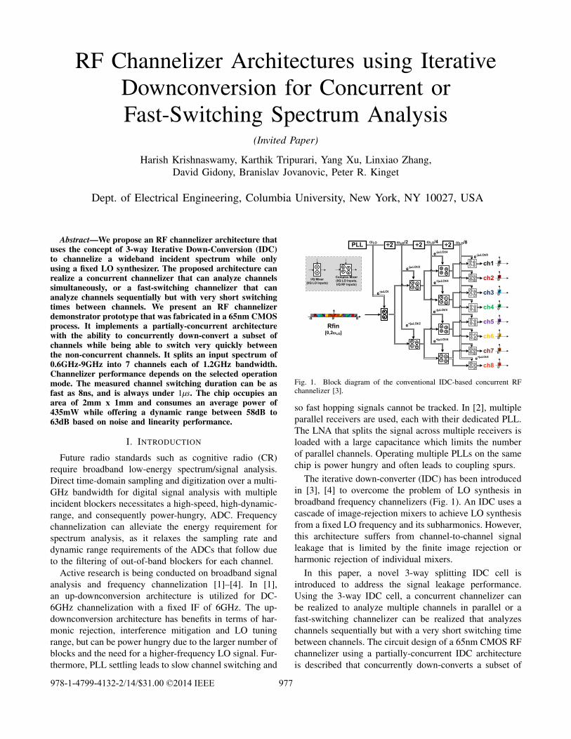
Fig. 2. Block diagram of a concurrent RF channelizer using the proposedthree-way splitting IDC stage.
the different channels as well as rapidly switches fromone non-concurrent channel to another. It decomposes aninput spectrum of 0.6GHz-9GHz into 7 channels, each of1.2GHz bandwidth, and produces 3 concurrent outputs.
II. PROPOSED 3-WAY-SPLITTINGPARTIALLY-CONCURRENT IDC ARCHITECTURE
In the conventional IDC-based concurrent RF channel-izer (Fig. 1), the effective LO in each branch of the IDC [3]is given by ωLO,eff =ωLO± ωLO
2 + ...+ωLO,N2N−1 where N is the
number of stages of frequency translation. However, withevery stage of mixing, signal leakage is introduced due tofinite image rejection and harmonic rejection. Harmonicrejection is typically limited to 30-40dB, which places afundamental limitation on the signal leakage. The use oftwo-stage HRMs is possible to achieve higher harmonicrejection. However, using them in every mixer becomes apower hungry solution.
A key insight is that for several channels in the conven-tional IDC, there is significant redundancy in the multiplefrequency translations used to finally obtain the channel atbaseband. For instance, RF signals around ωLO/2N−1 un-dergo N stages of frequency of translation instead directlybeing mixed with an LO of ωLO/2N−1. Similarly, signalsaround 2ωLO−ωLO/2N−1 undergo N stages of frequencytranslation. Instead they can be down-converted in twosteps using LOs of 2ωLO and ωLO/2N−1.
The three-way splitting IDC cell, shown in Fig. 2, min-imizes the number of frequency translations and performsonly downconversions. Output A processes the upper halfof the input spectrum by mixing the signal with 2ωLOand then filtering it. Output C filters out the lower half ofthe input spectrum without any mixing. Output B down-converts signals around the mid-band of the input signalusing an LO of ωLO. The addition of output B allows fora transition region between A and C so that the order oflowpass filters in A and C can be reduced without loosingfull spectral coverage. All the required LO frequenciescan still be obtained from a fixed LO synthesizer and itssubharmonics obtained by division by two.
By cascading three-way IDC cells a fully concurrent RFchannelizer can be realized as shown in Fig. 2. With twostages of IDCs, the input spectrum is split into 7 channelswhich are all available simultaneously. The signal leakagein a 2-way-IDC channelizer is limited by the harmonicrejection or image rejection of each mixer. This results insignal leakage in every channel . The proposed 3-way-IDCchannelizer minimizes the number of mixers in severalsignal paths. This results in significant improvement insignal leakage performance in these paths.
The fully-concurrent channelizer architecture can beconverted to a partially-concurrent, fast-switching archi-tecture by combining the paths of Output A and Out-put C. This is easily accomplished by implementing a“transparent mode” into the (passive) 2ωLO mixer, wherethe switches are all kept on for the transparent mode.The block diagram of the prototype 0.6GHz-9GHz 65nmCMOS partially-concurrent, fast-switching RF channelizerbased on such an architecture is shown in Fig. 3. It has twostages of the proposed 3-way-splitting IDC. The prototypehas 3 concurrent outputs instead of 7 (as is the case fora fully concurrent channelizer). Output 1 down-convertschannel 1 or 3 or 5 or 7, with an ability to rapidly switchbetween them. Output 2 down-converts channel 2 or 6,with an ability to rapidly switch between them. Output 3down-converts channel 4. Since only a fixed LO source isused, the speed of switching is limited by bias settling inmixers and buffer amplifiers and signal settling in filters.
III. CIRCUIT IMPLEMENTATION
Fig. 4 shows the circuit implementation of the variousblocks of the channelizer along the path to Channel 2/6.Current driven passive mixers are used throughout theprototype for their superior linearity. A differential front-end LNTA provides a 100-ohm input impedance (differ-ential) at the input interface of the chip and produces twoamplified concurrent outputs to the first stage of the IDC.One output is used for midband down-conversion usingthe 4.8GHz I/Q mixer to directly down-convert channel 4.The second LNTA output drives the 9.6GHz dual-modemixer, which can be operated either in transparent modeor in mixing mode. Based on its setting, either the loweror the upper part of the input spectrum is passed to thefilter. Passive LC based filters were chosen for realizingthe filtering considering the high frequency of operationand the superior linearity properties of an LC filter. Thecurrent buffer provides the appropriate load for the filtersand produces concurrent outputs once again for the second3-way IDC stage. In the second stage, one set of outputsof the current buffer (weighted as 1,
√2 and 1) drives the
2.4GHz harmonic-reject mixer and TIA to produce Output2, which can fast-switch between channels 2 and 6 (shownin Fig. 4). The other drives a 4.8GHz dual-mode “I/Q”mixer (enabled by the availability of more LO phases from
978

Fig. 3. Block diagram and chip microphotograph of the partially concurrent RF channelizer demonstration prototype with fast-switching using theproposed three-way splitting IDC stage.
(9.6GHz)
(2.4GHz)
(4.2GHz)
Fig. 4. Circuit implementation of various blocks of the RF channelizer along the path to Output 2, including the LNTA, 9.8GHz dual-mode mixer,5th order 4.2GHz LC filter, current buffer and 2.4GHz harmonic rejection mixer.
TABLE IRF CHANNELIZER MEASUREMENTS FOR P1DB, IIP3, NOISE FIGURE
AND COMPUTED NOISE FLOOR AND SFDRChannel 1 2 3 4 5 6 7
P1dB [dBm] -30.6 -21.7 -16.7 -21.3 -13.0 -13.8 -18.0IIP3 [dBm] -19.9 -12.4 -8.8 -12.5 -3.4 -5.5 -8.5NF [dB] 6.8 7.7 14.3 7.2 22.6 18.1 16.6
Noise Floor1 [dBm] -107.2 -106.3 -99.7 -106.8 -91.4 -95.9 -97.4SFDR [dB] 58.4 62.6 60.6 62.9 58.7 60.2 59.3
1 Noise bandwidth is assumed to be 1MHz
frequency division), filter, current buffer and a 1.2GHzharmonic-reject mixer and TIA to produce Output 1.
IV. MEASUREMENT RESULTS
Fig. 3 shows the die photo of the chip fabricated ina standard 65nm CMOS process. Table I presents themeasured P1dB, IIP3, and NF for the channels of the RFchannelizer. The spurious free dynamic range (SFDR) iscomputed as SFDR = 2
3 · (IIP3−NoiseFloor). A dynamicrange between 58dB to 63dB based on noise and linearityperformance is seen. Channel leakage measurements aredepicted in Fig. 5. While several channels exhibit expectedleakage performance, the leakage is degraded in somechannels because of unexpected spurs in some of themixers. The cause for these spurs is under investigation.
A. Concurrency
The RF Channelizer was experimentally verified tosupport concurrency: two signals were received simulta-
Fig. 6. (a) Measured BER of the RF channelizer receiving channel 1,while simultaneously receiving channel 2. (b) Measured BER of the RFchannelizer receiving channel 2, while simultaneously receiving channel1.
neously in Channel 1 and Channel 2. Fig. 6 shows themeasured BER vs incident desired signal power for variouspower levels of signal in the adjacent channel. A 200MbpsBPSK signal was used in each channel resulting in aaggregate data rate of 0.4Gbps for two channels.
B. Fast-switching
By avoiding PLL frequency switching, rapid channelswitching is enabled, and is now limited by the turn-ON/OFF times of the bias circuits in the signal pathblocks which include mixers and current buffers. Basedon measurements, the switching duration can be as fast as8ns and is always lower than 1µs. A further improvement
979
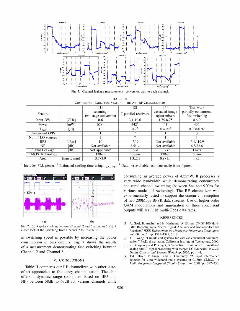
Fig. 5. Channel leakage measurements: conversion gain to each channel.
TABLE IICOMPARISON TABLE FOR STATE-OF-THE-ART RF CHANNELIZERS
[1] [2] [4] This work
Feature scanning,two-stage conversion 7 parallel receivers cascaded image
reject mixerspartially-concurrent,
fast-switchingInput BW [GHz] 0-6 3.1-10.6 1.75-8.75 0.6-9
Power [mW] 6781 3421 41 435Thop [µs] 10 0.22 few ns3 0.008-0.92
Concurrent O/Ps 1 7 1 3No. of LO sources 2 7 1 1
IIP3 [dBm] 10 -5/-9 Not available -3.4/-19.9NF [dB] Not available 2.5/14 Not available 6.8/22.6
Signal Leakage [dB] Not applicable 36-70 11-37 11-63CMOS Technology 130nm 130nm 130nm 65nm
Area [mm x mm] 3.7x3.9 1.3x2.7 0.8x1.1 1x2
1 Includes PLL power; 2 Estimated settling time using 1PLL−BW ; 3 Data not available, estimate made from figures.
(a) (b)Fig. 7. (a) Rapid switching between Channel 2 and 6 at output 2. (b) Acloser look at the switching from Channel 2 to Channel 6.
in switching speed is possible by increasing the powerconsumption in bias circuits. Fig. 7 shows the resultsof a measurement demonstrating fast switching betweenChannel 2 and Channel 6.
V. CONCLUSIONS
Table II compares our RF channelizer with other state-of-art approaches to frequency channelization. The chipoffers a dynamic range (computed based on IIP3 andNF) between 58dB to 63dB for various channels while
consuming an average power of 435mW. It processes avery wide bandwidth while demonstrating concurrencyand rapid channel switching (between 8ns and 920ns forvarious modes of switching). The RF channelizer wasexperimentally tested to support the concurrent receptionof two 200Mbps BPSK data streams. Use of higher-orderQAM modulations and aggregation of three concurrentoutputs will result in multi-Gbps data rates.
REFERENCES
[1] A. Goel, B. Analui, and H. Hashemi, “A 130-nm CMOS 100-Hz-6-GHz Reconfigurable Vector Signal Analyzer and Software-DefinedReceiver,” IEEE Transactions on Microwave Theory and Techniques,vol. 60, no. 5, pp. 1375–1389, 2012.
[2] Y.-J. Wang, “Circuits and systems for wireless concurrent communi-cation.” Ph.D. dissertation, California Institute of Technology, 2009.
[3] R. Gharpurey and P. Kinget, “Channelized front ends for broadbandanalog and RF signal processing with merged LO synthesis,” in IEEEDallas Circuits and Systems Workshop, 2009, pp. 1–4.
[4] T.-L. Hsieh, P. Kinget, and R. Gharpurey, “A rapid interferencedetector for ultra wideband radio systems in 0.13um CMOS,” inRadio Frequency Integrated Circuits Symposium, 2008, pp. 347–350.
980