Reversible Logic Synthesis Using a Non-blocking Order Search
71
Portland State University Portland State University PDXScholar PDXScholar Dissertations and Theses Dissertations and Theses 1-1-2010 Reversible Logic Synthesis Using a Non-blocking Reversible Logic Synthesis Using a Non-blocking Order Search Order Search Alberto Patino Portland State University Follow this and additional works at: https://pdxscholar.library.pdx.edu/open_access_etds Let us know how access to this document benefits you. Recommended Citation Recommended Citation Patino, Alberto, "Reversible Logic Synthesis Using a Non-blocking Order Search" (2010). Dissertations and Theses. Paper 162. https://doi.org/10.15760/etd.162 This Thesis is brought to you for free and open access. It has been accepted for inclusion in Dissertations and Theses by an authorized administrator of PDXScholar. Please contact us if we can make this document more accessible: [email protected].
Transcript of Reversible Logic Synthesis Using a Non-blocking Order Search

Portland State University Portland State University
PDXScholar PDXScholar
Dissertations and Theses Dissertations and Theses
1-1-2010
Reversible Logic Synthesis Using a Non-blocking Reversible Logic Synthesis Using a Non-blocking
Order Search Order Search
Alberto Patino Portland State University
Follow this and additional works at: https://pdxscholar.library.pdx.edu/open_access_etds
Let us know how access to this document benefits you.
Recommended Citation Recommended Citation Patino, Alberto, "Reversible Logic Synthesis Using a Non-blocking Order Search" (2010). Dissertations and Theses. Paper 162. https://doi.org/10.15760/etd.162
This Thesis is brought to you for free and open access. It has been accepted for inclusion in Dissertations and Theses by an authorized administrator of PDXScholar. Please contact us if we can make this document more accessible: [email protected].

Reversible Logic Synthesis Using a Non-blocking Order Search
by
Alberto Patino
A thesis submitted in partial fulfillment of the requirements for the degree of
Master of Science
in Computer Engineering
Thesis Committee: Marek Perkowski, Chair
Xiaoyu Song Christof Teuscher
Portland State University ©2010
i
Abstract
Reversible logic is an emerging area of research. With the rapid growth of
markets such as mobile computing, power dissipation has become an increasing
concern for designers (temperature range limitations, generating smaller transistors)
as well as customers (battery life, overheating). The main benefit of utilizing
reversible logic is that there exists, theoretically, zero power dissipation.
The synthesis of circuits is an important part of any design cycle. The circuit
used to realize any specification must meet detailed requirements for both layout
and manufacturing. Quantum cost is the main metric used in reversible logic. Many
algorithms have been proposed thus far which result in both low gate count and
quantum cost.
In this thesis the AP algorithm is introduced. The goal of the algorithm is to
drive quantum cost down by using multiple non-blocking orders, a breadth first
search, and a quantum cost reduction transformation. The results shown by the AP
algorithm demonstrate that the resulting quantum cost for well-known benchmarks
are improved by at least 9% and up to 49%.

ii
Dedication
I dedicate this thesis to my loving wife. Without her patience, support,
understanding, and most of all love, the completion of this work would not be
possible.

iii
Acknowledgments
I would like to show my gratitude to my advisor, Dr. Marek Perkowski, whose
passion for teaching guided me in my research. Also, I would like to thank Dr. Xiaoyu
Song and Dr. Christof Teuscher for participating in the thesis committee.

iv
Table of Contents
Abstract .................................................................................................................... i
Dedication ................................................................................................................ ii
Acknowledgments .................................................................................................. iii
List of Figures .......................................................................................................... vi
Glossary ................................................................................................................ viii
Chapter 1 ................................................................................................................. 1
Introduction ......................................................................................................... 1
Chapter 2 ................................................................................................................. 5
Background .......................................................................................................... 5
2.1 Boolean Logic Overview ............................................................................. 5
2.2 Basic Definitions ......................................................................................... 7
2.2.1 Reversible Logic Network Structure .................................................... 7
2.2.2 Reversible Gates ................................................................................ 10
2.2.3 Other Reversible Gates ...................................................................... 12
2.2.4 Positive Polarity Reed-Muller Expansion .......................................... 13
2.3 Measuring Quality of Reversible Gates .................................................... 15
2.3.1 Ancilla Bits ......................................................................................... 15
2.3.2 Delay .................................................................................................. 15
2.3.3 Quantum Cost .................................................................................... 16
Chapter 3 ............................................................................................................... 17
Previous Work on Reversible Logic Synthesis.................................................... 17
3.1 MMD (Maslov, Miller, and Dueck). .......................................................... 17
3.1.1 Algorithm .......................................................................................... 17
3.1.2 MMD Example ................................................................................... 19
3.1.2 MMD with Bidirectional Search ........................................................ 21
3.1.3 MMD Strengths and Weaknesses ..................................................... 24
3.2 Optimal Reversible Circuits ...................................................................... 25

v
3.3 PPRM Algorithm ....................................................................................... 26
3.3.1Algorithm ............................................................................................ 26
3.3.2 PPRM Algorithm Example .................................................................. 26
3.3.3 Strengths and Weaknesses of the Agrawal and Jha Algorithm ......... 28
3.4 Template Matching .................................................................................. 28
3.4.1 Overview ............................................................................................ 28
3.4.2 Template Matching Example ............................................................. 29
3.4.3 Strengths and Weaknesses ................................................................ 30
Chapter 4 ............................................................................................................... 32
AP Algorithm ...................................................................................................... 32
4.1 Motivation ............................................................................................... 32
4.2 AP Algorithm Overview ........................................................................... 33
4.3 Discovering New Options ........................................................................ 35
4.4 AP Algorithm Example ............................................................................ 38
4.5 AP Search ................................................................................................ 40
4.6 Quantum Cost Reduction ........................................................................ 43
Chapter 5 ............................................................................................................... 48
Results ................................................................................................................ 48
5.1 3-Variable Results .................................................................................... 48
5.2 Proposal for Better Quality Check ........................................................... 49
5.3 Benchmarks ............................................................................................. 52
5.4 Runtime ................................................................................................... 53
Chapter 6 ............................................................................................................... 55
Conclusion .......................................................................................................... 55
Chapter 7 ............................................................................................................... 57
Further Research ................................................................................................ 57
References ............................................................................................................. 60

vi
List of Figures
Figure 1 Truth Table Example ........................................................................................ 6
Figure 2 EXOR Operation ............................................................................................... 6
Figure 3 Basic EXOR Operations .................................................................................... 6
Figure 4 Reversible Specification ................................................................................... 8
Figure 5 Non-Reversible Specification ........................................................................... 9
Figure 6 Non-Reversible Specification Realized by reversible Logic ............................. 9
Figure 7 Reversible Logic Structure ............................................................................. 10
Figure 8 Tofolli Gates ................................................................................................... 11
Figure 9 TOF(A) ............................................................................................................ 11
Figure 10 TOF(A,B) ....................................................................................................... 11
Figure 11 TOF(A,B,C) .................................................................................................... 11
Figure 12 Fredkin Gates ............................................................................................... 12
Figure 13 Fred(A,B) ...................................................................................................... 12
Figure 14 FRED(C;A,B) .................................................................................................. 12
Figure 15 Peres Gate Operation .................................................................................. 12
Figure 16 Kerntopf Gate Operation ............................................................................. 13
Figure 17 Delay Equation ............................................................................................. 15
Figure 18 Quantum Circuit showing stages. The arrow denotes a feedback loop..... 16
Figure 19 MMD Implementation Direction ................................................................. 18
Figure 20 Example of applying MMD Basic Algorithm ................................................ 19
Figure 21 MMD Synthesis Example ............................................................................ 20
Figure 22 Bidirectional Algorithm Gate Direction ....................................................... 21
Figure 23 Bidirectional Example - MMD Algorithm ..................................................... 22
Figure 24 Bidirectional Example - MMD Circuit .......................................................... 22
Figure 25 Bidirectional Example - Bidirectional Algorithm ......................................... 24
Figure 26 Bidirectional Example - Circuit Result.......................................................... 24
Figure 27 PPRM Example Specification ....................................................................... 26
Figure 28 PPRM Example Search Tree Diagram .......................................................... 27
Figure 29 PPRM Example Realized Circuit ................................................................... 28
Figure 30 Specification - Template Matching Example .............................................. 29
Figure 31 Non-optimized Circuit.................................................................................. 29
Figure 32 Optimized Circuit after Template Matching ................................................ 30
Figure 33 3 Examples of Tofolli and Feynman Templates ........................................... 30

vii
Figure 34 Input/Search Relationship ........................................................................... 32
Figure 35 Decision Making if HD is Unequal ................................................................ 34
Figure 36 Synthesized Circuits of Unequal Hamming Distance ................................... 34
Figure 37 Discovering New Options - Example 1. ........................................................ 37
Figure 38 Discovering New Options - Example 2 ......................................................... 37
Figure 39 Detailed Steps on AP Basic Algorithm ......................................................... 39
Figure 40 Transformations taken during AP Basic Algorithm ..................................... 40
Figure 41 Synthesized Circuit using Basic AP Algorithm ............................................. 40
Figure 42 MMDS Search Diagram. ............................................................................... 41
Figure 43 AP Search Algorithm Detailed Steps ............................................................ 42
Figure 44 AP Search Algorithm Transformation Table ................................................ 42
Figure 45 Synthesized Circuit using AP Search Algorithm ........................................... 42
Figure 46 Comparison of MMD, AP Algorithm, and AP Algorithm Search. ................. 43
Figure 47 Circuit synthesized without QC Reduction .................................................. 44
Figure 48 Circuit synthesized with Quantum Cost Reduction ..................................... 46
Figure 49 Affects of QC Reduction on AP Algorithm in percentage ............................ 47
Figure 50 Results of applying all 3-variable functions to a number of algorithms. .... 49
Figure 51 Results of applying 40K random 4-variable functions in the AP Algorithm 51
Figure 52 Results of applying 40K random 5-variable functions in the AP Algorithm 51
Figure 53 Results of applying 40K random 6-variable functions in the AP Algorithm 52
Figure 54 AP Algorithm QC Analysis (MMD and ALHAGI) ........................................... 53
Figure 55 Runtime Analysis for AP Algorithm ............................................................. 54
Figure 56 No Transformation with quantum cost of 251 ............................................ 58
Figure 57 Transformation with 1 Ancilla bit with Quantum cost of 130 ..................... 58
Figure 58 Transformation with 2 Ancilla bit with Quantum cost of 95 ....................... 58
Figure 59 Transformation with 3 Ancilla bit with Quantum cost of 71 ....................... 59
Figure 60 Transformation with 4 Ancilla bit with Quantum cost of 61 ....................... 59

viii
Glossary
HD – Hamming Distance, which is the amount of bits that differ between 2 binary
specifications;
QC – Quantum Cost, which is a measurement of quality in a quantum circuit;
GC – Gate Count;
CNOT - Controlled NOT gate, also known as the Feynman gate;
LSB – Least Significant Bit
1
Chapter 1
Introduction
Since 1958, the semiconductor industry has successfully doubled the amount
of a transistors incorporated on an integrated-circuit every 2 years, but some experts
argue that Moore’s Law1 may be coming to an end in the next one or two decades.
Moving along with Moore’s law trend is the amount of heat dissipated in a single
device. While some of the dissipation can be minimized with manufacturing
optimization methods, other factors have yet to find a solution.
It has been shown by Landauer’s Principle2 that a circuit which is logically
reversible will, in principle, be thermodynamically reversible as well. He showed that
for every bit lost, kT * log2 joules of heat is generated. While this amount is
relatively small today, Zhirnov3 shows the difficulties in removing heat as CMOS
(Complementary metal–oxide–semiconductor) density increases, which has made
research in this area an important topic.
A circuit that results in no data lost is called reversible, hence would solve the
problem discussed by Landauer and will make this technology important in the
semiconductor world. Bennett4 showed that zero heat dissipation would only be
possible if a circuit was compromised of only reversible gates.
2
The most well-known application for reversible logic is quantum computing.
For any algorithm to be efficient, the execution time should not grow exponentially
as the number of inputs increase; instead, it should ideally grow as a polynomial
function. It has been shown that quantum computing is able to achieve this with
some exponentially hard problems, such as factorization (Shor’s Algorithm) 5 .
Quantum computation must be done using reversible logic6. Thus, research into the
synthesis of reversible logic is important as this could be the key factor resulting in
more powerful computers.
There have been a number of synthesis algorithms for reversible logic
proposed in recent years. Miller et all7 introduced a transformation based algorithm
(AKA MMD) in which steps were based on a truth table so that no transformation
would affect previous ones. Agrawal and Jha8 proposed a search algorithm using
ESOP PPRM minimization techniques. Kentopf9 introduced an algorithm based on
shared binary decision diagrams with complemented edges. Maslov recently
introduced two algorithms using Reed-Muller spectra10.
This thesis is organized as follows:
In Chapter 2, the basic concepts of reversible object are defined and
discussed. This includes basic Boolean logic, reversible gates, and

3
intermediate Boolean formulas. Popular methods to measure the quality of a
circuit design are also introduced.
The next chapter, Chapter 3, explains existing synthesis algorithms. Maslov’s
MMD algorithm is explained in great detail as well as its strengths and
weaknesses. This section is important to understand as these concepts are an
integral part of the later chapters.
Chapter 4 explains the new algorithm AP researched for this thesis. First, the
basic concept is explained, then, more complex algorithms are added on to
show how effective each step is. We also briefly touch on how this algorithm
compares to MMD.
Chapter 5 will show the results yielded from the new algorithm. The well
known quality check of checking all 3-variable function specifications will be
compared against other algorithms. The weakness of this quality check will
be discussed and new/better quality checks will be proposed, which will look
at larger circuits. Also, it will be shown that the AP Algorithm generates
circuits with low quantum costs when compared to other well known
algorithms.
The chapter Further Research will point the direction for further research in
the reversible logic synthesis area.
Finally, the conclusion will summarize the work discussed in this thesis.

4
My contributions to reversible logic technology are the following:
The AP algorithm which uses an MMD like algorithm which uses
Hamming Distance as a metric to yield more efficient results.
A search variant which explores many different circuits which result in
the same circuit output.
An algorithm which will compute all the possible vectors which can be
taken in the same cycle that will maintain a non-blocking vector
ordering.
A quantum cost reduction transformation that adds an extra ancilla bit
and reduces the size of the gates needed to complete the synthesis.

5
Chapter 2
Background
2.1 Boolean Logic Overview
Boolean logic is a logical algebra developed by George Boole where all
arguments and results of operators result in true or false. The most common
application of this type of math is in computer architecture and general digital logic
design.
Single-output Boolean logic functions of n variables are specified in the form
of truth tables, which have n+1 columns and rows. The columns are broken up
into n inputs and 1 output. The rows include all the combinations of the binary input
values in order to specify the complete behavior of the logic. Notice that the size of a
truth table is susceptible to explosion as the amount of inputs increases. This creates
an issue in computer programs as memory can quickly reach its limitation.

6
Figure 1 Truth Table Example
The main three gates used is classic Boolean logic are the AND, OR, and NOT
gates. The inputs to these gates are logical 1’s and 0’s. From these gates, any
Boolean formula can be derived. The logical operation exclusive disjunction, AKA
exclusive-or, can be derived and is extremely powerful. The operation of this
function will output ‘True’ when exactly one of the inputs is true, while all others are
false. The truth table for this function is shown in Figure 2 followed by some basic
operations for this gate in Figure 3, which is the basis of reversible logic gates.
Figure 2 EXOR Operation
Figure 3 Basic EXOR Operations
Input Output
a b c F
0 0 0 1
0 0 1 1
0 1 0 1
0 1 1 1
1 0 0 0
1 0 1 0
1 1 0 1
1 1 1 0
a b EXOR(a,b)
0 0 0
0 1 1
1 0 1
1 1 0

7
2.2 Basic Definitions
2.2.1 Reversible Logic Network Structure
There are quite a few rules that make reversible logic synthesis more
challenging than traditional binary logic synthesis. The following definitions outline
these differences.
Definition 2.1. A binary logic gate is reversible if the function it computes is bijective,
that is; each binary input pattern is mapped to a unique binary output pattern. Thus,
the circuit must have an equal amount of inputs and outputs.
As an example, the specification of a 3-input 3-output function from Figure 4
is a reversible specification. Notice that every single-output function from a multi-
input multi-output reversible function can always be in the form of

8
Figure 4 Reversible Specification
Definition 2.2. Every output of a gate that is irrelevant to the circuit functionality will
be considered a garbage signal.
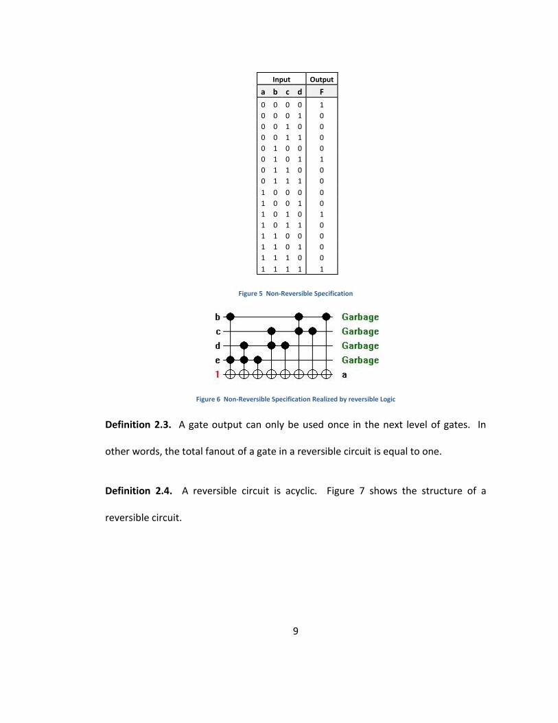
Let us consider the specification in Figure 5, which will be realized using
reversible logic. As specified in Definition 2.1, there must be an equal amount of
inputs and outputs. Since one output is considered, there will be at least 3 garbage
outputs in the realized circuit. In this case, a single ancilla bit is used, which means
there are 5 inputs and 4 garbage outputs as shown in Figure 6.
Input Output
x y z x' y' z'
0 0 0 0 1 0
0 0 1 1 0 0
0 1 0 0 1 1
0 1 1 0 0 0
1 0 0 0 0 1
1 0 1 1 1 0
1 1 0 1 1 1
1 1 1 1 0 1
9
Figure 5 Non-Reversible Specification
Figure 6 Non-Reversible Specification Realized by reversible Logic
Definition 2.3. A gate output can only be used once in the next level of gates. In
other words, the total fanout of a gate in a reversible circuit is equal to one.
Definition 2.4. A reversible circuit is acyclic. Figure 7 shows the structure of a
reversible circuit.
Input Output
a b c d F
0 0 0 0 1
0 0 0 1 0
0 0 1 0 0
0 0 1 1 0
0 1 0 0 0
0 1 0 1 1
0 1 1 0 0
0 1 1 1 0
1 0 0 0 0
1 0 0 1 0
1 0 1 0 1
1 0 1 1 0
1 1 0 0 0
1 1 0 1 0
1 1 1 0 0
1 1 1 1 1

10
Figure 7 Reversible Logic Structure
2.2.2 Reversible Gates
As definition 2.1 suggests, reversible logic does not use traditional logic gates
(AND, OR, XOR etc.). Instead, a new set is used with the following characteristics.
Definition 2.5. For the function variables { nxxx ,...,, 21 }, a Toffoli gate will use this
notation: TOF(C;t), where C = Control bits = { inii xxx ,...,, 21 } and t = { jx } and C t =
(empty set). The function of this gate will invert bit jx iff all variables in set C are
logically equal to ‘1’.
There are three forms where the Toffoli gate will be used: an inverter gate
denoted by TOF( jx ), the CNOT gate denoted by TOF ( ji xx ;1 ), commonly referred to
as a Feyman gate, and the original Tofolli gate denoted by TOF( inii xxx ,...,, 21 ; jx ). An
example of the gates discussed are shown in Figure 8. The equivalent functions in
traditional logic are shown in Figures 9,10, and 11.

11
Figure 8 Tofolli Gates
Figure 9 TOF(A)
Figure 10 TOF(A,B)
Figure 11 TOF(A,B,C)
Definition 2.6. For the function variables { nxxx ,...,, 21 }, a Fredkin gate will use this
notation: FRED(C;s), where C = Control bits = { inii xxx ,...,, 21 } and t = { 21, ss xx } and C
t = . The function of this gate will swap bits 21, ss xx iff all variables in set C are
logically ‘1’.
A Swap gate denoted by FRED( jx ), and the original Fredkin gate denoted by
FRED( inii xxx ,...,, 21 ; 21, ss xx ). Figure 12 will show the graphic notation for these two
gates. The equivalent gates using Toffoli gates are shown in Figures 13 and 14.

12
Figure 12 Fredkin Gates
Figure 13 Fred(A,B)
Figure 14 FRED(C;A,B)
2.2.3 Other Reversible Gates
The following is a brief overview of other gates that have been developed in
previous research.
The Peres gate11 can accomplish the same task as the CNOT gate and a 3-bit
Toffoli gate, with an operation defined in Figure 15.
Figure 15 Peres Gate Operation

13
The most common form of this gate is the 3-bit version defined in
Figure 15, but it can be extended to include multiple control lines. The 3-bit gate has
a quantum cost of 4.
The Kerntopf gate is a 3-bit gate with the operations defined in Figure 16. It
has the maximum number of subfunctions (cofactors). The usefulness of this gate is
still yet to be practically assessed as there are not many algorithms implemented in
software that include Kerntopf gate.
Figure 16 Kerntopf Gate Operation
2.2.4 Positive Polarity Reed-Muller Expansion
Any Boolean function can be converted into an xor sum of products. The
positive-polarity Reed-Muller expansion only uses variables which are
uncomplemented. PPRM is a canonical expression in the form :
nnnnnnnn xxxaxxaxxaxaxaxaaxxxf ............),...,,( 21...121121122211021
Where }1,0{ia , and ix are all uncomplemented variables.

14
PPRM is easily obtained from the xor sum of products by replacing any
complemented variable x with 1x and reducing the expression using laws of
Boolean logic. From this form, along with the use of well known Boolean algebra
methods the PPRM form can be realized. One motivator for using PPRM is the fact
that this form is unique and easy to minimize by eliminating redundant expressions.
To illustrate this, let us take the expression:
abababaa ' .
Now taking the PPRM form we can easily identify redundant expressions:
abaabbaa )1()1(1'
aaabbabbaa 1'
1' aa
The PPRM representation is an extremely powerful tool to use in software to
efficiently minimize equations as shown by the Agrawal and Jha algorithm8 for
reversible function specification.

15
2.3 Measuring Quality of Reversible Gates
2.3.1 Ancilla Bits
Ancilla bits are additional inputs that are not part of the original specification.
These bits are added in hopes to reduce the circuit complexity or realize a non-
reversible function. They come in the form of a constant logical 1 or 0.
It is ideal to keep the number of ancilla bits minimal due to the added circuit
complexity of having more inputs. In addition, the cost of adding ancilla bits could
outweigh the cost savings of reducing gate count of quantum cost.
The addition of ancilla bits cannot always be avoided. For instance, any non-
reversible specification will always need ancilla bits as it is otherwise impossible to
synthesize as a circuit with reversible gates.
2.3.2 Delay
The delay12 of a quantum circuit is defined with the equation in Figure 17.
Figure 17 Delay Equation
Where is dependent of the process technology and the depth is the number
of stages in the circuit. Stages in a quantum circuit are dependent on the number of
gates required to synthesize of specification. Figure 19 shows how the number of
stages is defined.

16
1 2 3 4 5Stage :
Figure 18 Quantum Circuit showing stages. The arrow denotes a feedback loop.
2.3.3 Quantum Cost
The quantum cost in a popular measurement used to compare different
reversible or logical circuits. The quantum cost of a reversible circuit is defined as the
number of primitive quantum gates needed to implement a reversible specification.
There are 2 methods that can be used to determine the quantum cost of a
reversible logic. First, the circuit can be realized using primitive quantum gates (1 x 1
and 2 x 2 gates) and then count the number of gates needed. Second, the circuit can
be realized using well know reversible gates whose quantum cost has already been
determined and the cost of each individual gates is summed. In this thesis, the latter
will be used.

17
Chapter 3
Previous Work on Reversible Logic Synthesis
3.1 MMD (Maslov, Miller, and Dueck).
3.1.1 Algorithm
MMD algorithm10 is currently the most popular synthesis algorithm for
reversible circuits. This method has been proven to be 100% convergent, that is, for
every circuit it is able to find a solution. The solution is guaranteed to yield a circuit
size of less than or equal to
The basic MMD algorithm can be completed in these steps7:
1. If then invert all the outputs that currently are logical 1’s using a
CNOT gate for each. This will ensure that .
2. Consider all other input/output combinations in order from to . If
, no transformation is needed. Otherwise, a transformation is
needed in order to make . The following sub-steps will
accomplish this:
a. Consider all positions in where a transformation from is
needed, for each of these, a Toffoli gate is needed whose target
line is that very position and the control lines are all lines that are
currently a logical 1.

18
b. Consider all positions in where a transformation from is
needed, for each of these, a Toffoli gate is needed whose target
line is that very position and the control lines are all lines that are
currently a logical 1.
Each gate derived from this algorithm in implemented from output to input.
If Gate m is that last gate which ensures that , then the first
gate in the circuit will be gate m.
Figure 19 MMD Implementation Direction
The main thing to note is this algorithm is that any Tofolli gate implemented
in will not affect any of the transformations that occurred in the previous steps.
In other words, once a row as successfully transformed , it will remain that
value regardless of what gate is implemented for the completion of the algorithm.
This is known as “control line blocking”.
Ga
te m
...
Ga
te 1
Input 1
Input 2
Input p
.
.
.
Output 1
Output 2
Output p
.
.
.
Gate Implementation Direction
19
3.1.2 MMD Example
Figure 20 Example of applying MMD Basic Algorithm
Figure 20 shows how the MMD basic algorithm in applied. In order to fully
understand this algorithm, each step will be discussed in closer detail. The notation
is as follows : C is the target line, 1 is a control line, X indicates this line is not used in
the gate.
Step i in the algorithm shows that since , then no NOT gates will be
used in this circuit.
In the output column, and the Hamming Distance is equal to 2.
Therefore, it will take 2 transformations (2 gates from step i and step ii) to
have . In this instance, only transformations for is needed
so the order does not matter. C11 and XC1 gates are used.

20
Now, in step ii column we see that . Since the Hamming Distance
is 1, then only one gate in needed for this transformation. A Feynman gate
C1X is applied.
In step iii, and the Hamming Distance in 1. A Feynman gate C11 is
applied in step iv.
In step iv, and the Hamming Distance in 2. In this instance, both
transformations are from , therefore order does not matter. Toffoli
gate 1C1 and Feynman gate 1XC are applied.
In step vi, and the Hamming Distance is equal to 1. The Toffoli
gate 1C1 is applied.
Now we see that and . The algorithm is complete and
no more transformations are needed.
Figure 21 shows the circuit which resulted from the above synthesis. The gate
count is equal to 7 and the total quantum cost is 17. Observe that the circuit was
built from outputs to inputs.
Figure 21 MMD Synthesis Example

21
3.1.2 MMD with Bidirectional Search
Introduced by Maslov7 is an MMD variant, the bidirectional method, and is a
natural progression of the original MMD algorithm as it addresses the weakness that
MMD only synthesizes the circuit from one direction, back to front. In this method,
for each step, it will be determined which direction (Figure 22) to synthesize based
on the Hamming Distance.
Figure 22 Bidirectional Algorithm Gate Direction
To illustrate how the bidirectional synthesis works, let us analyze the
following circuit specification using both traditional MMD and bidirectional MMD.
The MMD method yields a circuit with 9 gates and a quantum cost of 21 as shown in
Figures 23 and 24.

22
Figure 23 Bidirectional Example - MMD Algorithm
Figure 24 Bidirectional Example - MMD Circuit
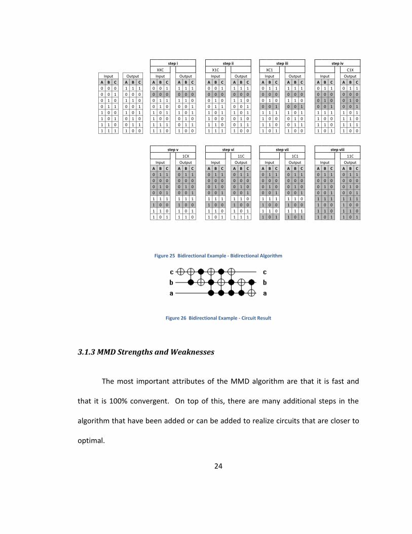
Using the bidirectional synthesis method, let us analyze the first 5 steps
(Figure 25) to understand the main differences between the traditional MMD and the
bidirectional method:
Step i – As seen above, the traditional MMD method would naively
synthesize the output side to match the input side. Notice that the HD
=3 in this case. Attempting to change the input side, we see that the
HD=1, and therefore, it is the better choice. Only one CNOT gate is
needed.
Step i Step ii Step iii Step iv Step v Step vi Step vii Step viii Step ix
Input
Output
CXX XCX XXC C11 XC1 X1C C11 11C 1CX A B C
A B C
0 0 0
1 1 1
011 001 000 000 000 000 000 000 000 0 0 1
0 0 0
100 110 111 011 001 001 001 001 001
0 1 0
1 1 0
010 000 001 001 011 010 010 010 010 0 1 1
0 0 1
101 111 110 110 110 111 011 011 011
1 0 0
1 0 1
001 011 010 010 010 011 111 110 100 1 0 1
0 1 0
110 100 101 101 111 110 110 111 101
1 1 0
0 1 1
111 101 100 100 100 100 100 100 110 1 1 1
1 0 0
000 010 011 111 101 101 101 101 111

23
Step ii and iii – In order to synthesize the binary equivalent of 1, both
directions show a HD of 2. The input choice is chosen because it has a
smaller number of one’s which could yield smaller gates.
Step iv - Looking at the binary equivalent of 3 from both directions,
we see that the input side has a HD=1 and the output side has a HD=2.
Therefore, we chose the input side.
The bidirectional algorithm yields a circuit (Figure 26) which is 1 gate less than
what MMD resulted. Clearly, the benefits of using a bidirectional method are
realized.
24
Figure 25 Bidirectional Example - Bidirectional Algorithm
Figure 26 Bidirectional Example - Circuit Result
3.1.3 MMD Strengths and Weaknesses
The most important attributes of the MMD algorithm are that it is fast and
that it is 100% convergent. On top of this, there are many additional steps in the
algorithm that have been added or can be added to realize circuits that are closer to
optimal.
step i
step ii
step iii
step iv
XXC
X1C
XC1
C1X
Input
Output
Input
Output
Input
Output
Input
Output
Input
Output
A B C
A B C
A B C
A B C
A B C
A B C
A B C
A B C
A B C
A B C
0 0 0
1 1 1
0 0 1
1 1 1
0 0 1
1 1 1
0 1 1
1 1 1
0 1 1
0 1 1
0 0 1
0 0 0
0 0 0
0 0 0
0 0 0
0 0 0
0 0 0
0 0 0
0 0 0
0 0 0
0 1 0
1 1 0
0 1 1
1 1 0
0 1 0
1 1 0
0 1 0
1 1 0
0 1 0
0 1 0
0 1 1
0 0 1
0 1 0
0 0 1
0 1 1
0 0 1
0 0 1
0 0 1
0 0 1
0 0 1
1 0 0
1 0 1
1 0 1
1 0 1
1 0 1
1 0 1
1 1 1
1 0 1
1 1 1
1 0 1
1 0 1
0 1 0
1 0 0
0 1 0
1 0 0
0 1 0
1 0 0
0 1 0
1 0 0
1 1 0
1 1 0
0 1 1
1 1 1
0 1 1
1 1 0
0 1 1
1 1 0
0 1 1
1 1 0
1 1 1
1 1 1
1 0 0
1 1 0
1 0 0
1 1 1
1 0 0
1 0 1
1 0 0
1 0 1
1 0 0
step v
step vi
step vii
step viii
1CX
11C
1C1
11C
Input
Output
Input
Output
Input
Output
Input
Output
A B C
A B C
A B C
A B C
A B C
A B C
A B C
A B C
0 1 1
0 1 1
0 1 1
0 1 1
0 1 1
0 1 1
0 1 1
0 1 1
0 0 0
0 0 0
0 0 0
0 0 0
0 0 0
0 0 0
0 0 0
0 0 0
0 1 0
0 1 0
0 1 0
0 1 0
0 1 0
0 1 0
0 1 0
0 1 0
0 0 1
0 0 1
0 0 1
0 0 1
0 0 1
0 0 1
0 0 1
0 0 1
1 1 1
1 1 1
1 1 1
1 1 0
1 1 1
1 1 0
1 1 1
1 1 1
1 0 0
1 0 0
1 0 0
1 0 0
1 0 0
1 0 0
1 0 0
1 0 0
1 1 0
1 0 1
1 1 0
1 0 1
1 1 0
1 1 1
1 1 0
1 1 0
1 0 1
1 1 0
1 0 1
1 1 1
1 0 1
1 0 1
1 0 1
1 0 1

25
One important attribute that lacks in this algorithm is the fact that it is not
scalable. As more and more variables are added into a specification, the memory
requirements grow exponentially. Also, there is a lack of search. We have seen in
many algorithms that it is impossible to know which step is the best gate selection
step, therefore, it is important to check all directions and get more than one result.
Then all results are analyzed and the most optimal is used.
3.2 Optimal Reversible Circuits
In 2003, Shende13 proposed an algorithm that resulted in a guaranteed
optimal circuit for any reversible logic specification. This algorithm requires the
generation of all optimal k-gate circuits as k increases for a logical specification π.
This is done using a depth first search technique in which additional gates will be
added after each step and checked for completion, if not, the process will continue.
Once the first correct circuit is discovered, the depth of the search will be limited to
that amount of gates.
While this algorithm is convergent as well guaranteeing the optimal result, it
requires memory space. Therefore, this algorithm can only work for, at most,
4-variable specifications. This limitation makes the algorithm an unrealistic solution
to synthesizing reversible logic, but it does give a bound of how well an algorithm can
perform.

26
3.3 PPRM Algorithm
3.3.1Algorithm
Agrawal and Jha8 developed an algorithm that uses the Reed-Muller
expansion for each individual output. During each step there exists n equations;
where n is the amount of inputs in the specification. Using the fact that all gates
result in the equation of , any possible gate that can be
extracted from the equation is done this way and implemented into all equations.
This process is repeated until a specification is discovered, there exists no more
possible gates to be included, or an infinite loop has been entered.
3.3.2 PPRM Algorithm Example
To understand the algorithm, the specification in Figure 27 will be analyzed:
Figure 27 PPRM Example Specification
Input
Output
A B C
A' B' C'
0 0 0
1 0 0
0 0 1
1 1 0
0 1 0
1 1 1
0 1 1
1 0 1
1 0 0
0 0 0
1 0 1
0 0 1
1 1 0
0 1 0
1 1 1
0 1 1

27
The first step is to convert the table into equations in the form of PPRM
(Section 2.2.4). From these equations, 3 different gates are implemented. Note that
we cannot apply a change to line with variable C because the equation does not have
the variable as a standalone.
The graph in Figure 29 shows only the first iterations of the algorithm which
finds a circuit rather quickly. The completed circuit (Figure 30) is identifiable by the
section where both sides of the equations are equal. This algorithm will continue its
search to see if there is a more optimal solution.
Figure 28 PPRM Example Search Tree Diagram
1' AA
ACCBB '
ACABBC '
AA '
ACBB '
ACABCC '
1' AA
ACBB '
ABBCC '
1' AACBB '
ACABBC '
AA '
BB '
ABCC '
AA 'ACABBB '
ACABCC '
AA '
BB '
CC '
1' AA
CBB
ACBB
ACBB
ABCC
ABCC

28
Figure 29 PPRM Example Realized Circuit
3.3.3 Strengths and Weaknesses of the Agrawal and Jha Algorithm
PPRM algorithm is stronger than other known methods due to the fact that it
has a search involved rather than stopping at the first result. Agrawal and Jha were
able to achieve near optimal results for all 3-variable specifications.
This algorithm was able to show full convergence on 3 and 4 variable
functions, but its evaluation found that a large number of 5-variable functions were
unable to converge. This could be due to time or memory constraints. Not being
able to show convergence on larger function is detrimental to the actual usage of this
algorithm in a real world environment.
3.4 Template Matching
3.4.1 Overview
In the previous section, some algorithms were discussed and the only one
which achieves guaranteed optimal results can only synthesize circuits which have at
most 3-4 variable inputs. This is the main motivation behind template matching; a
local optimization that can be applied to any circuit.
29
Basically, template matching analyzes a circuit and tries to find a specific
sequence of gates that can achieve the same logical results with lesser cost and no
adverse affects. This algorithm is very flexible since both the optimal and non-
optimal sequences live on an outside database.
3.4.2 Template Matching Example
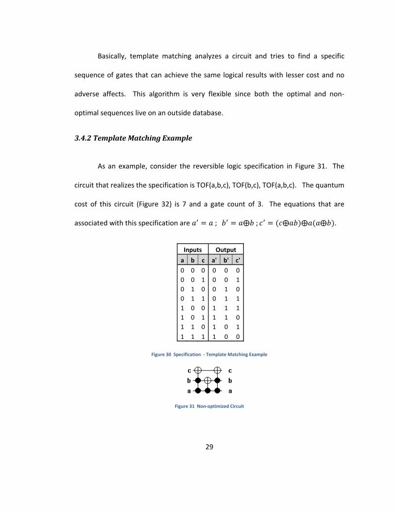
As an example, consider the reversible logic specification in Figure 31. The
circuit that realizes the specification is TOF(a,b,c), TOF(b,c), TOF(a,b,c). The quantum
cost of this circuit (Figure 32) is 7 and a gate count of 3. The equations that are
associated with this specification are .
Figure 30 Specification - Template Matching Example
Figure 31 Non-optimized Circuit
Inputs Output
a b c a' b' c'
0 0 0 0 0 0
0 0 1 0 0 1
0 1 0 0 1 0
0 1 1 0 1 1
1 0 0 1 1 1
1 0 1 1 1 0
1 1 0 1 0 1
1 1 1 1 0 0

30
The equation for c’ can be reduced using simple Boolean algebra:
. It is clear at this point that the circuit can be realized
using the sequence of gates: TOF(a,b), TOF(a,c), which is the optimized version of this
specification. This sequence of gates has a gate count of 2 and a quantum cost of 2.
This circuit is shown in Figure 33.
Figure 32 Optimized Circuit after Template Matching
Figure 34 shows some well known 2 and 3 variable templates.
Figure 33 3 Examples of Tofolli and Feynman Templates
3.4.3 Strengths and Weaknesses
Template matching has been shown to dramatically improve the size and cost
of reversible circuits. Maslov7 reported close to a 6% improvement when applied to
the MMD algorithm. This optimization result along with the fact that it can be

31
applied to any current and future algorithm makes this algorithm an extremely
powerful one.
Unfortunately, this extra step does take a longer time to apply as the number
of inputs increase as well as the gate count. Also, it is very difficult to have a
database with every single scenario which could be reduced to a more optimal
circuit. Furthermore, this algorithm requires several passes as when you change the
circuit, it is possible that another optimization has been uncovered.

32
Chapter 4
AP Algorithm
4.1 Motivation
The main motivation behind this new algorithm created by me and called AP
is to close the gap that MMD has left open. As shown by Stedman14, the natural
binary order actually falls into a subset of orderings that have the characteristics of
“control line blocking”. It was also shows that an exhaustive search of these
orderings results in a more efficient circuit. Unfortunately, an exhaustive search is
not a good option as the number of inputs increases because the number of orders
grows exponentially as shown in Figure 34.
Figure 34 Input/Search Relationship

33
4.2 AP Algorithm Overview
This algorithm follows the same high level flow as in MMD. The difference is
that there exists another level of intelligence instead of following a pre-defined
binary ordering. Before executing another iteration of the MMD algorithm, the
software checks all the options possible in order to maintain a non-blocking order.
Minimizing the amount of gates needed to synthesize this portion of the
circuit is the primary decision maker, which is done by choosing the combination that
has the smaller Hamming Distance. This is true due to the fact that there is a direct
correlation between the Hamming Distance and the amount of gates needed to
synthesize the circuit. In the case of tie, the input which contains the smallest
amount of logical 1’s will be chosen, which will minimize the quantum cost of the
gate. Figures 35 and 36 are examples showing how Hamming Distance and number
of logical 1’s affects the circuit.
Assume that these are the only 2 options for the next iteration of the circuit.
Option 2 clearly has a smaller Hamming Distance (HD) and will ultimately be the
chosen option. The decision to use the option with the smaller Hamming Distance is
justified as both synthesized circuits are shown below and option 2 is clearly the
smaller circuit.

34
The basic AP algorithm (intermediate improvement to MMD) is as follows:
1. If then invert all the outputs that currently are logical 1’s using a
cnot gate for each. This will ensure that .
2. Consider all the current options available. Calculate the Hamming
distance for each of these options and choose the one with the smallest
HD. If more than one options has the smallest HD calculation, randomly
choose one.
3. If , then no transformation is needed. Otherwise, a
transformation is needed in order to make . The following sub-
steps will accomplish this:
Option HD
a b c d e a b c d e
#1 1 0 0 1 0 0 1 1 1 1 4
#2 1 0 0 1 1 1 1 0 0 1 2
OUTPUTINPUT
Figure 35 Decision Making if HD is Unequal
Figure 36 Synthesized Circuits of Unequal Hamming Distance

35
a. Consider all positions in where a transformation from is
needed, for each of these, a toffoli gate is needed whose target
line is that very position and the control lines are all lines that are
currently a logical 1.
b. Now consider all positions in where a transformation from
is needed, for each of these, a Toffoli gate is needed whose
target line is that very position and the control lines are all lines
that are currently a logical 1.
4. Consider the current option. Determine what options have been
uncovered and consider them in step 2. If all , the algorithm in
complete.
Note that directly after step 1, there are certain options that are open
immediately. These options include all vectors that have exactly one logical one
while all other positions have logical zeros. Therefore, any circuit description which
has n inputs will have n options available immediately after step 1.
4.3 Discovering New Options
The main module in the AP algorithm is the one pertaining to discovering
what are the options available to use in the next iteration (see step 4 above). In
order to accomplish this, a history of every transformation must be kept in tables

36
separated by the number of logical 1’s in the transformation. The algorithm to
discover new options follows.
Assume the number of logical 1’s in the current choice is x.
1. Consider the current transformation and let p be all the positions where
there is a logical 1 and q be all the positions where there is a logical 0.
2. For all the previous transformations taken with x logical 1’s, consider only
transformations in which the number of differences in logical 1 positions
is only 1. Refer to these transformations as a subset p (which now
includes the current transformation).
3. Consider subset p, for each position p, count the number of logical 1’s.
a. If the count is less than x for any of the positions, then no new
options have been uncovered. There is no need to continue.
4. Consider subset p, for each position q, count the number of logical 1’s.
a. If the count is greater or equal to x, then a new option has been
uncovered where there is a logical one is all positions p and a
logical 1 located in the current position under consideration.
Figure 37 shows an example showing how the algorithm works in practice.
Consider that the current transformation that took place is vector 11100 and the
table shown below is the history of transformations taken place that have an equal
amount of logical ones.

37
As mentioned in step 3, we must consider all the positions in which there
exists a logical 1. In this case, we will be considering positions 1, 2, and 3. In order to
have a possibility of uncovering a new option, the count for all of these positions
must be equal to or greater than 3. As illustrated, the count for position 3 is only 2
and therefore, no new options have been discovered.
Let us know consider a similar example (Figure 39) to show how the algorithm
will work when new options can be discovered.
In this example, the result from step 3 will show that all the positions in
vector p have a logical 1 count of greater or equal to 3. Step 4 requires the algorithm
Figure 37 Discovering New Options - Example 1.
Figure 38 Discovering New Options - Example 2

38
to analyze all other positions (positions 4 and 5). From the table above, we see that
position 4 is only one, and therefore, no new option will be uncovered with a logical
1 in that position. Position 5, on the other hand, has a value which is greater or equal
to 3, and therefore, will result in a new option uncovered with a logical 1 is that
position along with logical 1’s in all positions in position p (Position 1, 2, and 3). The
new result is vector “11101”.
4.4 AP Algorithm Example
Figure 40 shows an example that demonstrates how the AP algorithm works.
For continuity, we will use the same example that was used in Chapter 3 which
outlines the basic MMD algorithm.
In Step 1, no action is needed as .
Since step 2 is the first iteration in which we must choose among options, we
must consider all possible vectors that contain exactly one logical 1. Option
“010” and “100” both have a HD = 1, therefore we will randomly choose
binary vector “100 “and make the transformation.
At this point, no new options are uncovered.
Step 3 will consider the remaining options. Between the 2 options available,
option “010” has the smaller HD and therefore will be used in the following
transformation.

39
The history of transformation now contains “100” and “010” which uncovers
a new option “110”.
In Step 4, consider the 2 options available and automatically take the option
with HD = 0, which requires no transformation.
In Step 5, there is only one available option in order to maintain a non-
blocking order. This option is used to make the transformation.
At this point, the entire transformation is complete. The result is shown in
Figure 40 and 41.
Figure 39 Detailed Steps on AP Basic Algorithm

40
Figure 40 Transformations taken during AP Basic Algorithm
Figure 41 Synthesized Circuit using Basic AP Algorithm
The circuit synthesized (Figures 41 and 42) shown above has a gate count of 5
and a quantum cost of 7. Compared to the basic MMD algorithm, this is a significant
improvement.
4.5 AP Search
In step 2 of the previous section, notice there were 2 options with an HD = 1.
In the basic algorithm, the option was chosen at random. By using randomness in an
algorithm, it is not easy to know if the transformation used results in the most
efficient circuit.
In this section, we introduce an AP Search Algorithm which is based on the
basic algorithm above. The search is a breadth-first search, illustrated in Figure 42,
Step 1 Step 2 Step 4
XXX 1XC C11 X1C XXX C11 XC1
A B C A B C
0 0 0 0 0 0 000 000 000 000 000 000 000
0 0 1 1 1 1 111 110 110 111 111 011 001
0 1 0 1 1 0 110 111 011 010 010 010 010
0 1 1 0 0 1 001 001 001 001 001 001 011
1 0 0 1 0 1 101 100 100 100 100 100 100
1 0 1 0 1 0 010 010 010 011 011 111 101
1 1 0 0 1 1 011 011 111 110 110 110 110
1 1 1 1 0 0 100 101 101 101 101 101 111
Step 3 Step 5
Input Output

41
and each node signifies a situation in which a random choice needed to be made due
to equivalent HD.
Figure 42 MMDS Search Diagram.
Figure 43 and 44 is the same example we used in the previous section. We
will not go through all the nodes in the search, but show what the results will be, if in
step 2 we would actually take the other option that was available.

42
Figure 43 AP Search Algorithm Detailed Steps
Figure 44 AP Search Algorithm Transformation Table
Figure 45 Synthesized Circuit using AP Search Algorithm
Step 1 Step 2 Step 3 Step 4 Step 5
XXX C1X 1XC XXX XC1
A B C A B C
0 0 0 0 0 0 000 000 000 000 000
0 0 1 1 1 1 111 011 011 011 001
0 1 0 1 1 0 110 010 010 010 010
0 1 1 0 0 1 001 001 001 001 011
1 0 0 1 0 1 101 101 100 100 100
1 0 1 0 1 0 010 110 111 111 101
1 1 0 0 1 1 011 111 110 110 110
1 1 1 1 0 0 100 100 101 101 111
Input Output

43
The synthesized circuit resulting from the search algorithm is shown in Figure
45. The gate count is 3 while the quantum cost is equal to 3. This is clearly the best
most reduced solution for this synthesis benchmark function.
Figure 46 is a summary of the synthesis methods for Basic MMD, Basic AP
Algorithm, AP Search on a single 3-variable circuit. Clearly, using a search results in a
better result as both the Gate Count and Quantum Cost are reduced.
Figure 46 Comparison of MMD, AP Algorithm, and AP Algorithm Search.
4.6 Quantum Cost Reduction
The AP algorithm, as is, works to reduce the overall gate count by minimizing
the HD for every step in the algorithm. While reducing the gate count can
0
2
4
6
8
10
12
14
16
18
Basic MMD Basic AP AP Search
Gate Count
Quantum Cost

44
significantly reduce the quantum cost, there is some transformation which can be
introduced into the AP algorithm to further reduce the quantum cost by adding a
single ancilla bit.
Let us analyze an example of a single step in the AP algorithm. Assume that
the next step is to transform the output from to , which are decimal
equivalents of a binary vector. By XORing these 2 numbers and counting the logical
ones, we see that the HD is 3 which means it will take 3 gates to properly complete
the transformation and have a quantum cost of 302. All figures in this section
assume that the LSB (least significant bit) is variable ‘a’.
Figure 47 Circuit synthesized without QC Reduction
Notice that the gates in this transformation (Figure 48) use variables <a, b, c>
as control lines. Since the quantum cost for Toffoli gates go up exponentially as the
number on inputs increases, it would be prudent to use smaller gates even if it
increases the amount of gates needed for the transformation. This notion justifies
the idea of combining the control lines in order to reduce the size of gates. This is
known as the Perkowski transformation.
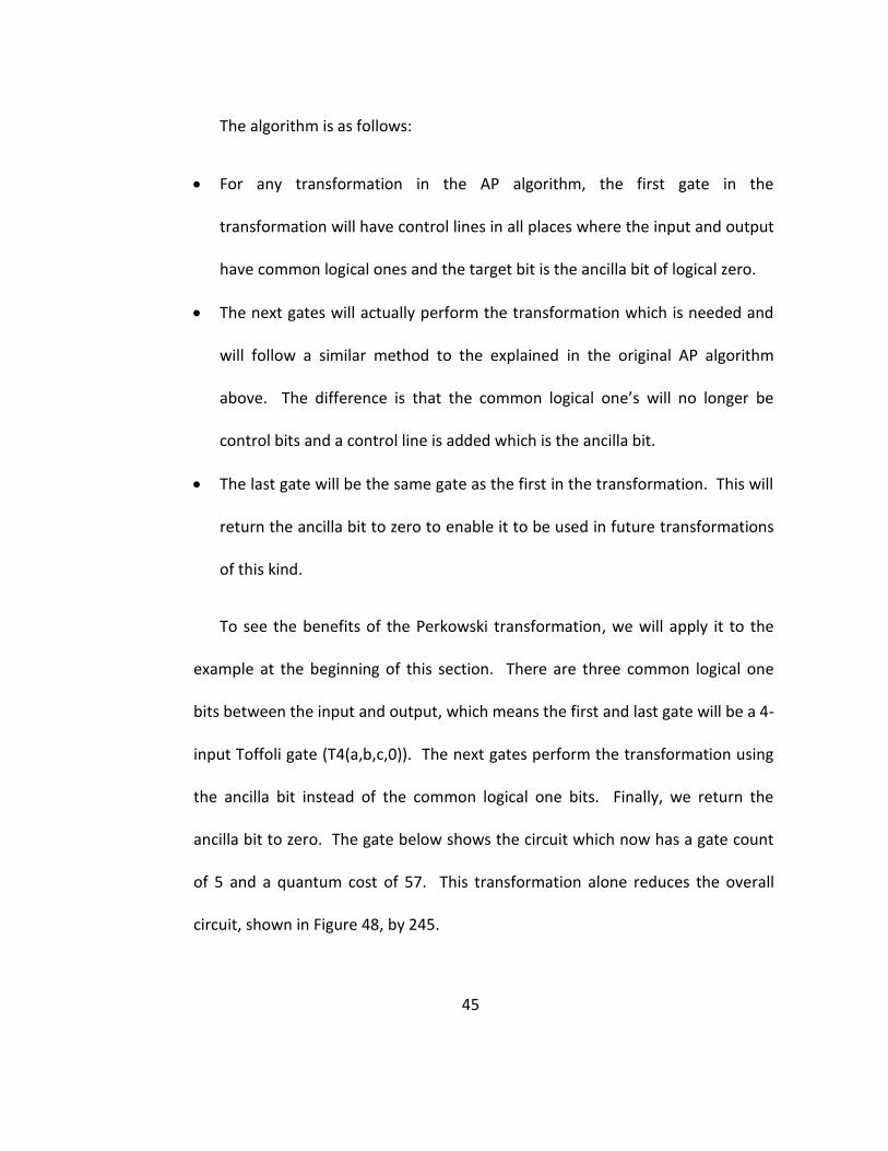
45
The algorithm is as follows:
For any transformation in the AP algorithm, the first gate in the
transformation will have control lines in all places where the input and output
have common logical ones and the target bit is the ancilla bit of logical zero.
The next gates will actually perform the transformation which is needed and
will follow a similar method to the explained in the original AP algorithm
above. The difference is that the common logical one’s will no longer be
control bits and a control line is added which is the ancilla bit.
The last gate will be the same gate as the first in the transformation. This will
return the ancilla bit to zero to enable it to be used in future transformations
of this kind.
To see the benefits of the Perkowski transformation, we will apply it to the
example at the beginning of this section. There are three common logical one
bits between the input and output, which means the first and last gate will be a 4-
input Toffoli gate (T4(a,b,c,0)). The next gates perform the transformation using
the ancilla bit instead of the common logical one bits. Finally, we return the
ancilla bit to zero. The gate below shows the circuit which now has a gate count
of 5 and a quantum cost of 57. This transformation alone reduces the overall
circuit, shown in Figure 48, by 245.
46
Figure 48 Circuit synthesized with Quantum Cost Reduction
Assuming we are transforming a circuit which has x inputs, y common logical
one bits between the inputs and outputs, and an HD of z. The z gates needed in the
main transformation will have y - 1 less control bits compared to the original
transformation rules. Therefore, any transformation which has only 1 common
logical one will not have any quantum cost optimization and should follow the
original transformations. Also, if a transformation only has an HD of 1, then the gate
needed for this transformation would be y + 1 in the original transformation method.
Since the Perkowski transformation applies 2 extra gates with the same quantum
cost, using the Perkowski transformation would actually yield a larger quantum cost.
Therefore, the Perkowski transformation should only be applied when the
current transformation has an HD ≥ 2 and the common logical one bits ≥ 2.
To understand how much improvement the QC minimization technique
results in, it was applied to a large number of benchmarks. The result shown in

47
Figure 50 clearly shows that the QC reduction provides much improvement to the AP
algorithm. In the case of an HWB18 benchmark, there is a 90% improvement of QC.
Note that the improvement grows as the number of inputs increase, which is
mostly due to the fact that the Toffoli gates QC increases exponentially as the
amount of control bits grows. You have to characterize all these benchmarks, tell the
source, how big is each of them in terms of number of variables and rows.
Figure 49 Affects of QC Reduction on AP Algorithm in percentage

48
Chapter 5
Results
5.1 3-Variable Results
One of the most common tests used to measure the quality of an algorithm is
how it performs across all 40,320 specifications for 3-variable functions. While this
test is not a good indication of the overall performance due to its lack of size, it does
serve as a gross check against other methods. The results here only serve to see how
close we can get to the optimal results9.
In Figure 50, we compare the AP algorithm vs. other well known methods as
well as the optimal circuits. Also included in the table is the progression of the
algorithm to illustrate how each addition to the algorithm includes the total gate
count.

49
Figure 50 Results of applying all 3-variable functions to a number of algorithms.
The results clearly show that using a bi-directional search with MMDS yields
the best results. Unfortunately, this AP algorithm does not create more optimized
gates when compared to other algorithms, but it does come somewhat close to
optimal results.
5.2 Proposal for Better Quality Check
The current quality check of using all 3-variable specifications is not enough to
check the overall quality of an algorithm because the circuits are too small. Using
specifications with a larger number of inputs will ensure that any proposed algorithm
has the ability to create optimized results for all kinds of specifications. The
challenge is that we cannot synthesize all specifications for circuits with more than 3
Gate Count AP AP/
Bi-direction
AP/ Bi-
direction/ Search MMD Agrewal/Jha
Reed Muller Spectra Optimal
0 1 1 1 1 1 1 1 1 12 12 12 12 12 12 12 2 79 88 93 102 102 102 102 3 344 442 508 567 625 625 625 4 1082 1539 1940 2125 2642 2780 2780 5 2599 3933 5196 5448 7479 8819 8921 6 4885 7235 9036 9086 13596 16953 17049 7 7215 9443 10175 9965 12476 10367 10253 8 8334 8699 8052 7274 3351 659 577 9 7422 5630 3972 3837 36 2 10 4949 2495 1175 1444 11 2371 692 153 391 12 793 105 7 62 13 193 6 6 14 37 15 4 AVG. Gate
Count 7.936 7.217 6.810 6.801 6.104 5.875 5.866
50
inputs, because the amount of specifications explodes. The solution to this problem
is to create random specifications and compare the average gate count across them.
Some would argue that this is problematic, because creating random specifications
means that different algorithms will not be able to ensure that the results are due to
the algorithm or the random specification that was used. In order to ensure that this
is not an issue, for each x-variable experiment, a large amount of specifications needs
to be included in the sample (ie 40,000 specifications). The resulting gate counts will
create a bell curve with a relatively small standard deviation. Unless any algorithm
can show a significant different in the average gate count, then we can consider the
results as equal.
Figures 51, 52 and 53 are the gate count results for reversible specifications
with inputs that are larger than 3.

51
Figure 51 Results of applying 40K random 4-variable functions in the AP Algorithm
Figure 52 Results of applying 40K random 5-variable functions in the AP Algorithm
0
1000
2000
3000
4000
5000
6000
7000
8000
9000
8 10 12 14 16 18 20 22 24 26
Nu
mb
er
of
Spe
cifi
cati
on
s
Gate Count
4 Input Variables
4 Input Variables
Average GC = 16.73
0
1000
2000
3000
4000
5000
6000
30 35 40 45 50
Nu
mb
er
of
Spe
cifi
cati
on
s
Gate Count
5 Variable Circuits
5 Input Variable
Average GC = 42.94

52
Figure 53 Results of applying 40K random 6-variable functions in the AP Algorithm
5.3 Benchmarks
The AP algorithm was applied to a number of benchmarks that were used in
both MMD and MP15 algorithms. Quantum Cost is the main parameter used to
compare the different algorithm since it expresses the actual cost of implementation.
Due to the fact that the size of the circuits grows exponentially as the number
of inputs increases, it was decided to show the results as the precentage quantum
cost compared to the MMD basline. For instance, for the HWB4 benchmark, Alhagi,
Hawash and Perkowski15 show an increase of 30% compared to MMD and the AP
algorithm shows a decrease of about 50% compared to MMD.
0
500
1000
1500
2000
2500
3000
3500
4000
88 93 98 103 108 113 118 123
Nu
mb
er
of
Spe
cifi
cati
on
s
Gate Count
6 Variable Circuits
6 Variable Circuits
Average GC = 109.95

53
Of the 10 benchmarks used the AP algorithm shows that it produces better
results for 9 of them. The exact results are shown in Figure 54.
Figure 54 AP Algorithm QC Analysis (MMD and ALHAGI 15)
5.4 Runtime
A good property of any CAD tool is a minimal runtime. The graph from
FIGURE 55 shows THAT the AP algorithm can successfully provide results within 10
minutes for up to 16 variables. The time to synthesize will grow linearly with the
amount of searches requested. Unfortunately, as the amount of inputs increases,
the time to synthesize grows exponentially, which significantly limits this algorithms
ability to synthesize specifications that require input variables greater than 18 input
variables.

54
Figure 55 shows the results of running the hidden-weighted benchmark
across many different sizes.
Figure 55 Runtime Analysis for AP Algorithm
0
10
20
30
40
50
60
70
80
90
4 5 6 7 8 9 10 11 12 13 14 15 16 17 18
Min
ute
s
Input Variables
AP Algorithm Runtime
55
Chapter 6
Conclusion
The thesis starts off by analyzing previous work accomplished by Maslov et al
and Jha et al to synthesize reversible specifications. Part of this analysis includes an
understanding of the strengths and weaknesses of each algorithm in order to lay the
ground work for a new algorithm which can provide better results.
Chapter 4 introduces the AP algorithm which uses the same underlying
concepts as those used in MMDS, but improves synthesis by exploring more than one
non blocking order and by prioritizing lower Hamming Distance transformations.
These 2 additions successfully reduce the overall gate count, which directly reduces
the quantum cost.
Unfortunately, this reduction in quantum cost is not enough. Section 4.4
introduces the Perkowski transformation which can perform the same
transformation per cycle, but at the cost of adding an extra Ancilla bit and 2 Toffoli
gates.
Next, the results of the AP algorithm are compared against MMD7, RELOS8,
and the MP algorithm15. The results show the AP algorithm significantly reduces the
quantum cost. Also, the current quality check of checking all 3 variable specifications
is challenged. A new check is proposed to randomly select a large sample of n>3
56
variable reversible function specifications. The AP algorithm results should serve as a
baseline for future algorithms since this is the first algorithm to report these types of
results.
The AP algorithm successfully provides 4 out of the 4 highly desirable
properties which make a good CAD tool:
1. Reliability: The AP algorithm will 100% convergent which means that it will
always provide a solution even if it is not optimal.
2. Quality: Optimal or near-optimal networks are the goal of synthesis reversible
specifications. The results of the AP algorithm show significant reduction in
quantum cost, which has been shown to be one of the most desirable quality
indicators.
3. Runtime: The time needed to synthesize is relatively small. While the
runtime is extremely dependant on the amount of transformation needed as
well as the amount of searches requested. Keeping the searches below 50,
we see a runtime of just 1 hour for functions using 15 input variables. It is
important to note that this time grows exponentially as the amount of inputs
increases, which is not desirable.
4. Scalability: This algorithm has the ability to synthesize functions of up to 20
input variables. The main limiting factor is the size of the truth tables which
need to be stored in memory.

57
Chapter 7
Further Research
The AP algorithm successfully drives down the quantum cost of the
synthesized circuits by applying a single Ancilla bit. This method can be recursively
applied to any cycle in the synthesis process for this algorithm. For instance, assume
we are transforming the output from to . The AP algorithm, without
adding any transformation, will result in a circuit, shown in Figure 56, with quantum
cost of 251.
As discussed in section 4.4, a transformation can be used which will add an
extra Ancilla bit which will effectively reduce the quantum cost to 130. This circuit is
shown in Figure 57.
The next logical step would be to analyze the gates which are not used to
transform the single Ancilla bit to see if we can continue adding transformations and
add more Ancilla bits. The process should continue until no more transformations
can be accomplished. Figures 58 and 59 show the resulting circuits when more
ancilla bits are applied. Figure 60 shows the final circuit with the maximum
transformations. The circuit illustrates that by adding up to 4 ancilla bits, a circuit
with quantum cost of 61 can be achieved.

58
Figure 56 No Transformation with quantum cost of 251
Figure 57 Transformation with 1 Ancilla bit with Quantum cost of 130
Figure 58 Transformation with 2 Ancilla bit with Quantum cost of 95

59
Figure 59 Transformation with 3 Ancilla bit with Quantum cost of 71
Figure 60 Transformation with 4 Ancilla bit with Quantum cost of 61
As with the most improvements to a circuit, it does not come free. In this
case, the extra ancilla bits must be added for every transformation to be added.
There has been little to no research done on the actual cost of extra Ancilla bits. This
type of research is critical to the future research in synthesizing quantum circuits.

60
References
1 Gordon E. Moore, Cramming more Components onto Integrated Circuits, Electronics,
38(8), April 9, 1965. 2 R. Landauer, Irreversibility and heat generation in the computing process, IBM Journal of
Research and Development, v.5 n.3, p.183-191, July 1961 3 Zhirnov, V. V., Kavin, R. K., Hutchby, J. A., and Bourianoff, G. I. 2003. Limits to binary logic
switch scaling--a Gedanken model. Proc. IEEE, 91 11, 1934-1939. 4 C. H. Bennett, Logical reversibility of computation, IBM Journal of Research and
Development, v.17 n.6, p.525-532, November 1973 5 I. Chuang, "Experimental realization of a Shor-type quantum algorithm," in International
Conference on Quantum Information, 2001 OSA Technical Digest Series (Optical Society of America, 2001), paper FQIPA3.
6 V. Vedral, A. Barenco, and A. Ekert. Quantum networks for elementary arithmetic
operations. Phys. Rev. A, 54: 147-153, 1996 7 D. Michael Miller , Dmitri Maslov , Gerhard W. Dueck, A transformation based algorithm for
reversible logic synthesis, Proceedings of the 40th conference on Design automation, June 02-06, 2003, Anaheim, CA, USA , p. 318-323.
8 Agrawal, A. and Jha, N. K. 2004. Synthesis of reversible logic. In Proceedings of the
Conference and Exhibition on Design, Automation, and Test in Europe. p.21384–21385. 9 P. Kerntopf, .A new heuristic algorithm for reversible logic synthesis,. in Proc. Design
Automation Conf., June 2004, pp. 834.837. 10 D. Maslov , G. W. Dueck , D. M. Miller, Techniques for the synthesis of reversible Toffoli
networks, ACM Transactions on Design Automation of Electronic Systems (TODAES), v.12 n.4, p.42-45, September 2007
11 A. Peres, 1985. Reversible logic and quantum computers. Phys. Rev. A 32, p.3266–3276. 12 M. Mohammadi , M. Eshghi, On figures of merit in reversible and quantum logic designs,
Quantum Information Processing, v.8 n.4, p.297-318, August 2009
13 V V Shende, Prasad, A. K.,Markov,I. L. and Hayes 2003. Synthesis of Reversible logic
Circuits. IEEE Trans. Comput. Aid Des. 226, p.723-729. 14 Ch. Stedman, B. Yen and M. Perkowski, Synthesis of Reversible Circuits with Small
Ancilla Bits for Large Irreversible Incompletely Specified Multi-Output Boolean Functions, Proc. 14th International Workshop on Post-Binary ULSI Systems, May 18, 2005, Calgary, Canada.

61
15 N. Alhagi, M. Hawash, M. Perkowski, "Synthesis of Reversible Circuits with No Ancilla Bits
for Large Reversible Functions Specified with Bit Equations," ISMVL, p.39-45, 2010 40th IEEE International Symposium on Multiple-Valued Logic, 2010