Reststrahl band-assisted photocurrents in epitaxial graphene layers688497/FULLTEXT01.pdf ·...
8
Reststrahl band-assisted photocurrents in epitaxial graphene layers P. Olbrich, C. Drexler, L. E. Golub, S. N. Danilov, V. A. Shalygin, Rositsa Yakimova, S. Lara-Avila, S. Kubatkin, B. Redlich, R. Huber and S. D. Ganichev Linköping University Post Print N.B.: When citing this work, cite the original article. Original Publication: P. Olbrich, C. Drexler, L. E. Golub, S. N. Danilov, V. A. Shalygin, Rositsa Yakimova, S. Lara-Avila, S. Kubatkin, B. Redlich, R. Huber and S. D. Ganichev, Reststrahl band-assisted photocurrents in epitaxial graphene layers, 2013, Physical Review B. Condensed Matter and Materials Physics, (88), 24, 245425. http://dx.doi.org/10.1103/PhysRevB.88.245425 Copyright: American Physical Society http://www.aps.org/ Postprint available at: Linköping University Electronic Press http://urn.kb.se/resolve?urn=urn:nbn:se:liu:diva-103289
Transcript of Reststrahl band-assisted photocurrents in epitaxial graphene layers688497/FULLTEXT01.pdf ·...
Reststrahl band-assisted photocurrents in
epitaxial graphene layers
P. Olbrich, C. Drexler, L. E. Golub, S. N. Danilov, V. A. Shalygin, Rositsa Yakimova, S.
Lara-Avila, S. Kubatkin, B. Redlich, R. Huber and S. D. Ganichev
Linköping University Post Print
N.B.: When citing this work, cite the original article.
Original Publication:
P. Olbrich, C. Drexler, L. E. Golub, S. N. Danilov, V. A. Shalygin, Rositsa Yakimova, S.
Lara-Avila, S. Kubatkin, B. Redlich, R. Huber and S. D. Ganichev, Reststrahl band-assisted
photocurrents in epitaxial graphene layers, 2013, Physical Review B. Condensed Matter and
Materials Physics, (88), 24, 245425.
http://dx.doi.org/10.1103/PhysRevB.88.245425
Copyright: American Physical Society
http://www.aps.org/
Postprint available at: Linköping University Electronic Press
http://urn.kb.se/resolve?urn=urn:nbn:se:liu:diva-103289

PHYSICAL REVIEW B 88, 245425 (2013)
Reststrahl band-assisted photocurrents in epitaxial graphene layers
P. Olbrich,1 C. Drexler,1 L. E. Golub,2 S. N. Danilov,1 V. A. Shalygin,3 R. Yakimova,4 S. Lara-Avila,5 S. Kubatkin,5
B. Redlich,6 R. Huber,1 and S. D. Ganichev1
1Terahertz Center, University of Regensburg, 93040 Regensburg, Germany2Ioffe Physical-Technical Institute, Russian Academy of Sciences, 194021 St. Petersburg, Russia
3St. Petersburg State Polytechnic University, 195251 St. Petersburg, Russia4Linkoping University, S-58183 Linkoping, Sweden
5Chalmers University of Technology, S-41296 Goteborg, Sweden6Radboud University Nijmegen, Institute for Molecules and Materials, FELIX Facility, Toernooiveld 7,
6525 ED Nijmegen, The Netherlands(Received 1 August 2013; published 17 December 2013)
We report on the observation of the reststrahl band-assisted photocurrents in epitaxial graphene on SiC excitedby infrared radiation. The peculiar spectral dependence for frequencies lying within the reststrahl band of theSiC substrate provides a direct and noninvasive way to probe the electric field magnitude at atomic distancesfrom the material’s surface. Furthermore our results reveal that nonlinear optical and optoelectronic phenomenain two-dimensional crystals and other atomic scale structures can be giantly enhanced by their deposition on asubstrate with negative dielectric constant.
DOI: 10.1103/PhysRevB.88.245425 PACS number(s): 78.67.Wj, 42.70.Nq, 73.50.Pz, 81.05.ue
I. INTRODUCTION
Since the discovery of graphene, optical and optoelectronicproperties of two-dimensional (2D) crystals have attractedcontinuously growing attention.1 A keen interest has beenmotivated by the prospective application of mono- or few-layer systems in nonlinear optics,2–6 solar cells,7 displays,8
optoelectronics,9 sensors,10,11 or plasmonic devices.12,13
Bridging the size mismatch between macroscopic photonicsand atomic-scale integrated electronics all these concepts uni-versally depend on a key quantity: the local optical fields actingon the charge carriers in 2D systems. These fields deviate fromthe emitted or incident waves due to the dielectric environmentof the supporting substrate. A mesoscopic description has beeninvoked to obtain electromagnetic fields in the vicinity of afictitious effective medium characterized by a mathematicallysharp interface and bulk dielectric functions.12–15 Yet, in theextreme limit of an atomically thin system a mesoscopic modelis not justified a priori and electromagnetic fields may bealtered by the modified polarization response of the surfacestructure.
At the same time, the precise knowledge of the localelectromagnetic fields is particularly important for phenomenathat scale nonlinearly with the field amplitude. Examplesrange from optical nonlinearities to high-frequency transportas studied in 2D crystals,2–6,12–20 carbon nanotubes,21–24 topo-logical insulators,25–27 and single molecules.28 Nonetheless,measuring electric fields on atomic distances is challenging.Surface-confined plasma oscillations in graphene have beenshown to change their dispersion sensitively in the spectralvicinity of the reststrahl band29 of substrates.30 They could,thus, be basically used as sensors for the local dielectric envi-ronment. However, plasmon polaritons or phonon polaritonsextend over comparably large distances into the substrate andinto the air rather than being localized at a two-dimensionallayer. Their properties depend on the entire dielectric envi-ronment over a layer of a thickness of tens to hundreds ofnanometers towards either side of the graphene sample.31 Even
for near-field microscopy reaching extreme subwavelengthspatial resolution13,32 or a recent approach tracing the naturaloptical-frequency magnetic dipole transitions in lanthanideions,33 the atomic scale has been out of reach.
Here, we demonstrate that measurements of photoelectriceffects in graphene deposited on a substrate provide a directway to probe the electric field magnitude at atomic distancesfrom the material’s surface. We show that second-orderphotoelectric effects excited in graphene exhibit a peculiarspectral dependence for frequencies lying within the reststrahlband of the SiC substrate. The resonances of the photocurrentsare attributed to the variation of the out-of-plane and in-planecomponents of the radiation electric field acting on electronsthat are confined in the graphene layer deposited at a distanced ≈ 2 A from the SiC surface (see Fig. 1 and Ref. 34). Ouranalysis of the field distribution based on the macroscopicFresnel formulas surprisingly well describes all experimentalfindings, while there remain quantitative discrepancies. Asan important result, the observed reststrahl band-assistedphotocurrent also clearly demonstrates that nonlinear opticaland optoelectronic phenomena in 2D crystals can be giantlyenhanced by a proper combination of the spectral range andsubstrate material.
II. EXPERIMENTAL DETAILS ANDSAMPLES PREPARATION
Photocurrents have been observed in large area n-type graphene monolayer samples17,35 at room temperature.Figure 1(a) depicts the experimental geometry. Radiation wasapplied in the (xz) plane at an angle of incidence θ , variedbetween −30◦ and +30◦ to the layer normal, z. The signalsgenerated in the unbiased devices were measured via anamplifier with 20 MHz bandwidth and recorded with a stor-age oscilloscope. The photocurrents were induced applyingmidinfrared radiation of the frequency tunable free electronlaser “FELIX” at FOM-Rijnhuizen in the Netherlands.36,37
The laser operated in the spectral range between 7 and 15 μm
1098-0121/2013/88(24)/245425(7) 245425-1 ©2013 American Physical Society

P. OLBRICH et al. PHYSICAL REVIEW B 88, 245425 (2013)
FIG. 1. (Color) (a) Experimental geometry. (b) Reflection of aplane wave from a graphene layer on a SiC substrate deposited atdistances of about 2 A from the surface.
(corresponding to photon energies from �ω ≈ 180 to 90 meV).The output pulses of light from FELIX were chosen to be ≈2 pslong with peak power P ≈ 150 kW, separated by 1 ns, in atrain (or “macropulse”) of 5 μs duration. The beam has analmost Gaussian profile with a spot diameter of about 1 mm,which is measured by a pyroelectric camera.38,39 The laser spotwas always smaller than the sample size allowing us to avoidillumination of contacts or sample edges and, consequently, tostudy only photocurrents generated in pristine graphene.17 Theradiation intensity I and electric field E0 on the sample duringthe micropulse were about 20 MW/cm2 and 120 kV/cm,respectively. The macropulses had a repetition rate of 10 Hz.The room temperature photoresponse was studied in thedirections perpendicular and parallel to the light incidenceplane. The results obtained applying the radiation of FELIXprovide the full information about functional behavior of thephotocurrent, however, the evaluation of the current magnitudein response to such short pulses is not straightforward. Thus, tocalibrate the photocurrent response we additionally measuredthe current excited by the radiation of a line-tunable continuouswave CO2 laser with power P of about 40 mW. Thoughoperating in a narrower spectral range (from 9.2 to 10.8 μm)it provides radiation in the vicinity of the upper limit ofthe reststrahl band and, therefore, is appropriated for thedetermination of the photocurrent value in the spectral regionunder study. The radiation power was controlled by a photondrag detector40 and/or a mercury cadmium telluride detector.
The experiments were carried out on several largearea graphene monolayer samples epitaxially grown onthe Si-terminated face of a 4H-SiC(0001) semi-insulatingsubstrate16,41 at T = 2000 ◦C and 1 atm argon gas pressure.42
The layers are n doped due to the charge transfer fromSiC with a measured electron concentration in the rangeof 1.5 × 10¹² to 7 × 1012 cm−2, Fermi energy EF rangingfrom 160 to 300 meV, and mobility of about 103 cm2/V sat room temperature.16–18 The samples are characterized bya strong structure inversion asymmetry as demonstrated bythe study of the magnetic quantum ratchet effect.35 Squareswith dimensions of 5 × 5 mm2 were patterned on grapheneusing standard electron beam (e-beam) lithography and oxygenplasma etching. Four metallic contacts on the periphery ofgraphene were produced by straightforward deposition ofTi/Au (3/100 nm) through a lithographically defined mask,followed by lift-off. Ohmic contacts have been prepared at thecenter of the edges, with a resistance of about 2 k� betweenopposed contacts.
FIG. 2. (Color) Spectra of the photocurrent excited by (a) linearlyand (b) circularly polarized radiation.
III. EXPERIMENTAL RESULTS
Illuminating an unbiased graphene layer with polarizedradiation at oblique incidence we detected a photocurrentsignal whose spectral behavior is shown in Fig. 2. Panel(a) shows the photocurrent jL
y excited by linearly polarizedradiation with the angle between the polarization vector andthe plane of incidence α = ±45◦. A remarkable observationis that the current in the range of photon energies �ω betweenabout 99 and 120 meV changes sign while its value increasesby more than an order of magnitude compared to that excitedby light with lower and higher frequencies. Despite the factthat the photocurrent shows a peculiar spectral dependenceits overall functional behavior remains unchanged in thewhole frequency range: The current (i) scales linearly withthe radiation intensity I ∝ E2
0 , (ii) is characterized by a shortresponse time, and (iii) varies with the angle α and the angle ofincidence θ as jL
y = L sin 2α sin θE20 , where L is a prefactor.
Besides the transversal photocurrent discussed in the paper,linearly polarized radiation also excites a current flowingalong the light propagation direction, which varies as jL
x =L cos 2α sin θ E2
0 (not shown). The spectral dependence ofthe latter photocurrent is shown in Fig. 3 exhibiting reso-nancelike behavior similar to the transversal one. A helicity-dependent photocurrent was not detected in longitudinalgeometry. The overall functional behavior of the longitudinalphotocurrent is in agreement with the phenomenologicaltheory and microscopic picture of the photon drag andphotogalvanic effects.16,18
Studying the radiation reflection reveals that the positionand width of the photocurrent resonance matches well thereststrahl band of the SiC,30,43 which is characterized by analmost total reflection R(ω) between the longitudinal, �ωLO,
245425-2

RESTSTRAHL BAND-ASSISTED PHOTOCURRENTS IN . . . PHYSICAL REVIEW B 88, 245425 (2013)
α = 0°|θ| = 30°
j L x /I
(arb
. uni
ts)
jx
θ2
1
-1
0
100 120 140 ħω (meV)
ћωTO ћωLO
13 12 11 10 9 λ (μm)8
FIG. 3. (Color online) Spectra of the longitudinal photocurrentjLx measured for |θ | = 30◦ and the azimuth angle α = 0◦. The data
are obtained applying linearly polarized radiation of the free electronlaser “FELIX.” Gray area indicates the range of the reststrahl band ofSiC. The inset shows the experimental geometry.
and transversal, �ωTO, optical phonon energies. Figure 4 showsthe reflection spectra of graphene and SiC samples. It is seenthat the reflection spectra of graphene layer on SiC slightlydeviates from that of the pure SiC substrate (see dotted line inFig. 4). This result is in agreement with the data of Ref. 30 andis attributed to the substrate phonon-induced surface plasmon-polariton formation in epitaxial graphene.
The photocurrent is also observed for elliptically (circu-larly) polarized radiation, obtained via rotation of the Fresnelrhombus by the angle ϕ. By that we controllably vary thedegree of linear, Pl = (sin 4ϕ)/2, and circular, Pc = sin 2ϕ,polarization, respectively. Figure 5(a) shows the polarizationdependence of jy measured in the vicinity of �ωLO. Thedetected photocurrent can be well fitted by jy = jL
y + jCy =
[(L/2) sin 4ϕ + C sin 2ϕ] sin θ E20 as shown in Figs. 5(b) and
5(c) for photon energies below and above �ωLO, respectively.Here the linear photocurrent jL
y , given by the fourth harmonicsof ϕ, is just the above discussed current in response to linearlypolarized radiation but excited by elliptically polarized light.The circular current jC
y stems from the radiation helicityand is proportional to Pc. Figure 5 reveals the crossoverfrom the dominating circular (∝sin 2ϕ) to linear (∝sin 4ϕ)photocurrent contributions in the vicinity of �ωLO. The spectralbehavior of the circular contribution jC is shown for right-handed circular polarization in Fig. 2(b). Similar to the linearphotocurrent, we found here a peculiar spectral behavior withinthe reststrahl band. However, by contrast to jL
y , the circular
Ref
lect
ion
(%) 100
50
75
25
0100 120 140 ћω (meV)
5.0
7.5
2.5
0.0
-2.5
substrate (SiC)graphene
on SiC ћωTO
ћωLO
ΔR (%
)
13 12 11 10 9 λ (μm)8
FIG. 4. (Color online) Dashed and solid lines show the reflectionspectra of graphene on SiC substrate and pure SiC, respectively.Dotted line shows the difference between the two curves. The spectraare measured with a Fourier spectrometer. Gray area shows the rangeof the reststrahl band of SiC limited by the energies of transverse andlongitudinal optical phonons.
Angle φ0° 45° 90° 135° 180°
110
120
130
Phot
on e
nerg
y ћω
(meV
) -0.35 0.35
jy / I (arb. units)
ћω =129 meV
ћω =116 meV
ћω =129 meV
Angle φ 0° 45° 90° 135° 180°
ћω =116 meV
0.3
0.0
-0.3
j y /
I (ar
b. u
nits
)
0.3
0.0
-0.3
ћωLO
= -30°(a)
(b)
(c)
σ+ σ-
FIG. 5. (Color) (a) Photocurrent jy/I as a function of �ω andangle ϕ (polarization states are sketched above). (b) and (c) showcorresponding dependencies obtained for fixed �ω.
photocurrent is not enhanced but rather suppressed. It has acomplex spectral behavior exhibiting a change of sign and apeak close to the center of the reststrahl band.
IV. DISCUSSION
The microscopic origin of the photocurrent outside of thereststrahl band has been previously investigated in Ref. 18.It has been demonstrated that the current is caused by a sumof the photon drag (PDE) and photogalvanic (PGE) effects ofcomparable strength. In particular, it has been shown that thephoton drag effect in graphene is caused by a simultaneousaction of the electric and magnetic field components of theinfrared radiation and, in fact, can be classified as a dynamicHall effect.16,18 The origin of the PGE is the asymmetry ofelectron scattering induced by radiation and structure inversionasymmetry.18,44,45 The addressed above fact that all charac-teristic features of the photocurrent are the same within andoutside the reststrahl band, indicates that its microscopic originremains unchanged. Actually, this is not surprising because for�ω � EF and room temperature no resonances are expectedfor the light-matter interaction in pristine graphene. However,one can expect dramatic modifications of local electric fieldsacting on carriers in graphene for frequencies within thereststrahl band of the substrate, which is characterized bya negative dielectric constant of the material. Indeed thecoincidence of the increased reflection with the observedresonance of the photocurrent clearly indicates the commonorigin of both effects.
As we show below, the resonant photoresponse can be wellunderstood considering only the spectral behavior of the in-plane and out-of-plane radiation electric field components,without going into microscopic details. The required electricfield components responsible for the photocurrent formationprovide the phenomenological theory of PDE and PGE. In linewith the experiment we consider the transverse photocurrentjy generated in the direction perpendicular to the incidenceplane (xz). Following Ref. 6 the current density due to the
245425-3
P. OLBRICH et al. PHYSICAL REVIEW B 88, 245425 (2013)
photon drag effect is given by
jPDEy = T qx(ExE
∗y + E∗
xEy) + T ′qxi(EyE∗x − ExE
∗y ), (1)
and due to the photogalvanic effect by
jPGEy = χ (EzE
∗y + EyEz
∗) + γ i(EzE∗y − EyEz
∗). (2)
Here E is the electric field acting on electrons, and T and χ
are coefficients describing, respectively, the linear PDE andPGE. These currents are proportional to the linear polarizationdegree Pl given by symmetrical combinations of electric fieldcomponents. The two remaining coefficients correspond tothe circular PDE (T ′) and PGE (γ ) currents, which reversethe direction upon switching the photon helicity given byi(E × E∗)/|E|2 · q/q.
In the following analysis we assume coefficients χ , γ ,T , and T ′ to be frequency independent in the studiednarrow frequency range and focus on the frequency variationof the electric field components only. This assumption isreasonable for the considered experimental conditions becausefor room temperature, �ω � EF, and ωτ ∼ 1, the radiationabsorption is caused by Drude-like indirect intraband opticaltransitions, and hence, χ , γ , T , and T ′ have smooth frequencydependencies.16,18 Moreover, we disregard a possible influ-ence of graphene itself on the electric field magnitudes.
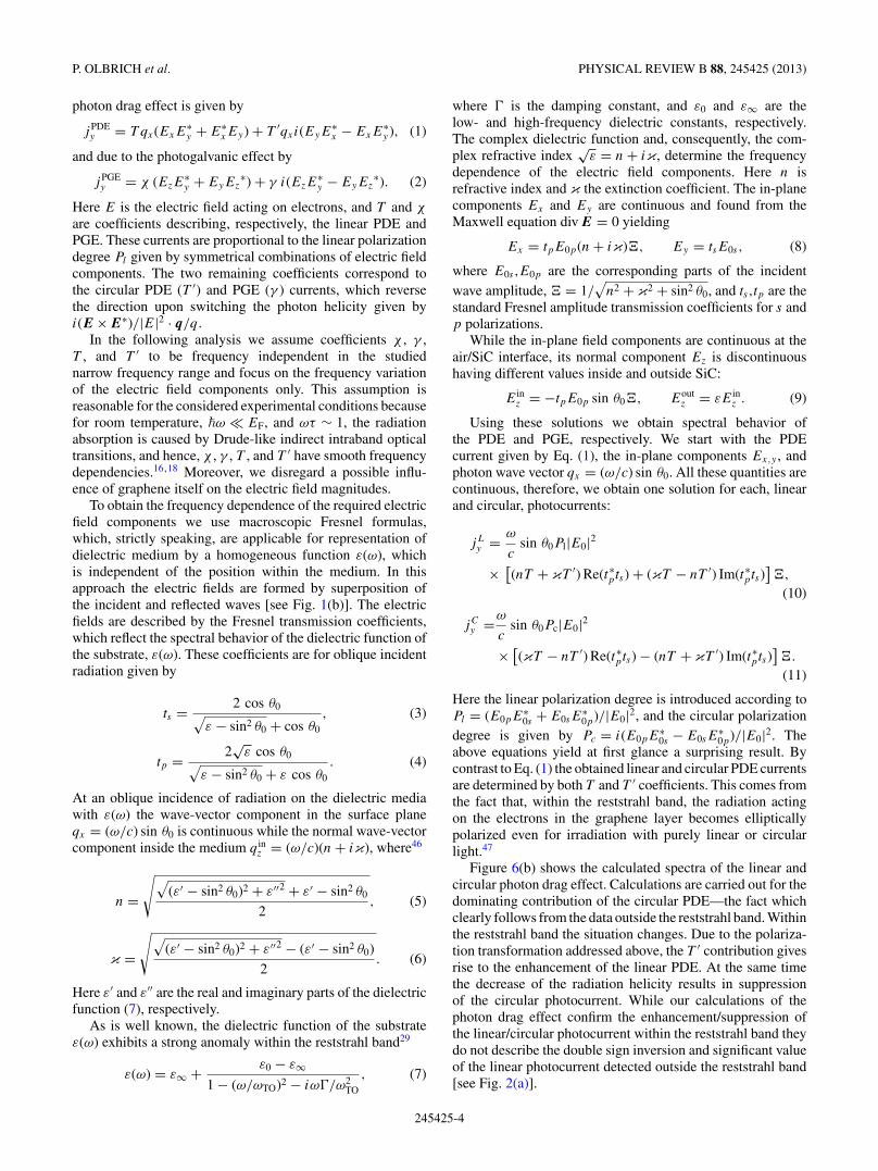
To obtain the frequency dependence of the required electricfield components we use macroscopic Fresnel formulas,which, strictly speaking, are applicable for representation ofdielectric medium by a homogeneous function ε(ω), whichis independent of the position within the medium. In thisapproach the electric fields are formed by superposition ofthe incident and reflected waves [see Fig. 1(b)]. The electricfields are described by the Fresnel transmission coefficients,which reflect the spectral behavior of the dielectric function ofthe substrate, ε(ω). These coefficients are for oblique incidentradiation given by
ts = 2 cos θ0√ε − sin2 θ0 + cos θ0
, (3)
tp = 2√
ε cos θ0√ε − sin2 θ0 + ε cos θ0
. (4)
At an oblique incidence of radiation on the dielectric mediawith ε(ω) the wave-vector component in the surface planeqx = (ω/c) sin θ0 is continuous while the normal wave-vectorcomponent inside the medium q in
z = (ω/c)(n + iκ), where46
n =√√
(ε′ − sin2 θ0)2 + ε′′2 + ε′ − sin2 θ0
2, (5)
κ =√√
(ε′ − sin2 θ0)2 + ε′′2 − (ε′ − sin2 θ0)
2. (6)
Here ε′ and ε′′ are the real and imaginary parts of the dielectricfunction (7), respectively.
As is well known, the dielectric function of the substrateε(ω) exhibits a strong anomaly within the reststrahl band29
ε(ω) = ε∞ + ε0 − ε∞1 − (ω/ωTO)2 − iω�/ω2
TO
, (7)
where � is the damping constant, and ε0 and ε∞ are thelow- and high-frequency dielectric constants, respectively.The complex dielectric function and, consequently, the com-plex refractive index
√ε = n + iκ, determine the frequency
dependence of the electric field components. Here n isrefractive index and κ the extinction coefficient. The in-planecomponents Ex and Ey are continuous and found from theMaxwell equation div E = 0 yielding
Ex = tpE0p(n + iκ)�, Ey = tsE0s , (8)
where E0s ,E0p are the corresponding parts of the incidentwave amplitude, � = 1/
√n2 + κ2 + sin2 θ0, and ts ,tp are the
standard Fresnel amplitude transmission coefficients for s andp polarizations.
While the in-plane field components are continuous at theair/SiC interface, its normal component Ez is discontinuoushaving different values inside and outside SiC:
Einz = −tpE0p sin θ0�, Eout
z = εEinz . (9)
Using these solutions we obtain spectral behavior ofthe PDE and PGE, respectively. We start with the PDEcurrent given by Eq. (1), the in-plane components Ex,y , andphoton wave vector qx = (ω/c) sin θ0. All these quantities arecontinuous, therefore, we obtain one solution for each, linearand circular, photocurrents:
jLy = ω
csin θ0Pl|E0|2
× [(nT + κT ′) Re(t∗pts) + (κT − nT ′) Im(t∗pts)
]�,
(10)
jCy =ω
csin θ0Pc|E0|2
× [(κT − nT ′) Re(t∗pts) − (nT + κT ′) Im(t∗pts)
]�.
(11)
Here the linear polarization degree is introduced according toPl = (E0pE∗
0s + E0sE∗0p)/|E0|2, and the circular polarization
degree is given by Pc = i(E0pE∗0s − E0sE
∗0p)/|E0|2. The
above equations yield at first glance a surprising result. Bycontrast to Eq. (1) the obtained linear and circular PDE currentsare determined by both T and T ′ coefficients. This comes fromthe fact that, within the reststrahl band, the radiation actingon the electrons in the graphene layer becomes ellipticallypolarized even for irradiation with purely linear or circularlight.47
Figure 6(b) shows the calculated spectra of the linear andcircular photon drag effect. Calculations are carried out for thedominating contribution of the circular PDE—the fact whichclearly follows from the data outside the reststrahl band. Withinthe reststrahl band the situation changes. Due to the polariza-tion transformation addressed above, the T ′ contribution givesrise to the enhancement of the linear PDE. At the same timethe decrease of the radiation helicity results in suppressionof the circular photocurrent. While our calculations of thephoton drag effect confirm the enhancement/suppression ofthe linear/circular photocurrent within the reststrahl band theydo not describe the double sign inversion and significant valueof the linear photocurrent detected outside the reststrahl band[see Fig. 2(a)].
245425-4

RESTSTRAHL BAND-ASSISTED PHOTOCURRENTS IN . . . PHYSICAL REVIEW B 88, 245425 (2013)
SiC substratey
xz
(a )b()
(c) (d)100 120 140 ћω (meV)
ħωTO ħωLO
yyyyyyyyyyyyyyyyyyyyyyyyyyyyyyyyyyyyyyxxxxxxxxxxxxxxxxxxxxxxxxxxxxxxxxxxxxzzzzzzzzzzzzzzzzzzzzzzz
(((((((((((((((((((((((((((((aaaaaaaaaaaaaaaaaaaaaaaaaaaaaaaaa )))))))))))))))))))))))))))))bbbbbbbbbbbbbbbbbbbbbbbbbbbb((((((((((((((((((((((((((((((()))))))))))))))))))))))))
(c((c((((c(c(c(c(c(c(c(ccc(cc(c((c((c(c(ccc(c((c(ccc(c(c((( ))))))))))))))))))))))))))) (d(d(dd(d((d(d(d(dd(d(d((d(d(d(d(dd((ddddd((d(d(d(d(d(d(d(((( )))))))))))))))))))))))))))))1010101001010101000101000011000000010000000010000 00000000000000000000000000000000 11111111111112022020020202200202020220202020202020202020202002202020202202002022202020 14114414141414141411444414444144444440000000000000000000000000000000000000000 ћωћћωћωћωћћћωћωћћћωћωћћωћωћωћωћωћωћωћωћωћωћωωћωωћћωωωћωћωћћωωћωћћωћћωћωћωћωωω ((((((((((((((((((((((((((((((((((memmemememememmmmemememeememmemmmmmemeemmmeeeemeeemeeV)V)V)VV)V)V)V)V)VV)V)V)V)VV))VV)V)VVVV)V)))VVV)VV))V))))
ħωħħωħωħωħωħωħωħωħωħωħħħωħωħωħωħωħωħωħωħωħωωħωħωħωħωħωħωωħωħωωħωħωħωħħωωħħħ TOTOOTOTOOOOOOOOTOOOOOOTOOOOOOOOOOOOOOOOOOOOOOOOOOOOOOOOOO ħωħωħωħωħωħωħħωħωħωħħωħħħωħωħωħħωħωħωħωħωħωωωħωħħωωωωħħħωħωħωωħωωωωħħωωωωωLOLOLOOOLOOOLOOOOOOOOOLOOLOOOOLOOLOOOO
FIG. 6. (Color) (a) Experimental geometry. (b)–(d) Calculatedspectra of the linear (solid) and circular (dashed) photocurrents.(b) Photon drag effect. (c) and (d) Photogalvanic effect caused bythe electric field in the SiC side, Ein, and in the air side of theair/SiC interface, Eout, respectively. The calculations are performedfor θ0 = 30◦, γ /χ = 0.9, and T ′/T = 18, as well as obtained fromthe reflection data � = 0.01 ωTO, ε∞ = 6.52, and ε0 = 9.66 for SiC(see also Ref. 43). The insets shows the electric field componentsconsidered in the calculations.
To obtain a better agreement we consider the photogalvaniceffect which, according to Ref. 18, should yield a comparablecontribution to the total photocurrent excited by infraredradiation. It follows from Eq. (2) that all PGE contributionsrequire a normal component of the electric field, which isdiscontinuous at the interface. Therefore, from Eqs. (2) and(9) we obtain different solutions for the photocurrents inducedby the field in the air side of the air/SiC interface, Eout
z :
jLy = − sin θ0Pl|E0|2[χ Re(t∗pts) + γ Im(t∗pts)]�, (12)
jCy = − sin θ0Pc|E0|2[γ Re(t∗pts) + χ Im(t∗pts)]�, (13)
and from the field in the SiC side of the interface, Einz :
jLy = − sin θ0Pl|E0|2[χ Re(t∗pε∗ts) + γ Im(t∗pε∗ts)]�, (14)
jCy = − sin θ0Pc|E0|2[γ Re(t∗pε∗ts) + χ Im(t∗pε∗ts)]�. (15)
The resulting calculations, applying the same parameters asthat used for the PDE, are shown in Figs. 6(c) and 6(d).It is seen that both linear and circular PGE show a strongenhancement in the reststrahl band. The solutions for theelectric field in the substrate [see Fig. 6(c)] yield a sharp peakclose to �ωLO only and, thus, do not describe the complexspectral behavior of the photocurrent. Moreover, we did notdetect any sharp peak at LO frequency, which supports theconclusion that this contribution to the total photocurrent isnegligible. Good agreement with the experiment is obtainedfor the linear PGE excited by the electric field in the air sideof the air/SiC interface [see Fig. 6(d)]. However, this solutiondoes not describe the suppression of the circular photocurrent.
FIG. 7. (Color online) Spectral behavior of the linear (solid lines)and circular (dashed lines) photocurrents. (a) Experimental results.(b) Calculations of the total photocurrent considering electric fieldcomponents Ex,Ey and electric field component in the air side ofthe air/SiC interface Eout
z . Here we used a ratio of circular PDE tocircular PGE equal to (ωT O/c)T ′/χ = 0.3 and the parameters givenin the caption of Fig. 6.
We emphasize that this disagreement cannot be avoided simplyby variation of the coefficients γ and χ .
Our calculations show that overall reasonable agreementcan only be achieved by considering a superposition of bothPDE and PGE photocurrents and taking into account thez component of the electric field in the air side of theair/SiC interface. The corresponding results together withexperimental data are shown for transversal photocurrent inFig. 7. In fact, the calculations reflect all main features of themeasured photocurrent, namely, (i) both circular and linearcurrents depend weakly on the frequency outside the reststrahlband; (ii) the linear current changes its sign and has a broadpeak within the whole reststrahl band; (iii) the circular currentis suppressed and has a peak at �ω ≈ 115 meV; and (iv) thelinear current dominates the circular one within the reststrahlband and vice versa in the outside. We emphasize that asatisfying agreement is obtained despite the fact that thecalculations are carried out for the homogeneous functionsε(ω), abrupt interfaces, and the disregarded influence ofgraphene on the radiation field. These simplifications used inour model or possible Ez electric field induced charge transferbetween graphene and SiC48 may be responsible for remainingsmall discrepancies. A comparison of the linear PDE and PGEcomponents reveals that within the resonance the photon drageffect strongly dominates in the total current, whereas outsidethe resonance the main contribution comes from the linearPGE. As for the circular photocurrent the PDE is responsiblefor the photoresponse in the whole studied spectral range.
In the above analysis the magnitudes and spectral behaviorof particular electric field components have been calculatedafter Eqs. (8) and (9) using the set of parameters given inthe caption to Fig. 6. The complex spectral behavior of thedielectric constant epsilon within the reststrahl band [seeEq. (7)] results in the enhancement of particular electric fieldcomponents. As an example the ExEy product changes by afactor of 8.4 upon variation of radiation frequency from ω
lying outside the reststrahl band (ω = 0.5ωTO) to that withinthe restrahl band (ω = 1.2ωTO) where the maximum of this
245425-5

P. OLBRICH et al. PHYSICAL REVIEW B 88, 245425 (2013)
product is reached. While it is tempting to assume, a priori,that the electric field in the vicinity of a surface is “simply”determined by the Fresnel formulas, this approach, aftercareful consideration, is not trivial. In fact, the derivation of theFresnel formulas assumes interfaces of fictitious homogeneousdielectric media described by dielectric functions. In the fieldof optics this assumption is usually valid since the wavelengthsof light as well as penetration depths of evanescent wavesexceed interatomic distances by several orders of magnitude.On an atomic length scale, however, the physics could bequite different at surfaces, because the local polarizabilityof the single atomic layer may deviate from the bulkvalues.
V. SUMMARY
To conclude, our results demonstrate that photocurrents ingraphene deposited on a medium with a negative dielectricconstant can be efficiently used for studies of how an electricfield acts on the atomic scale. While the described approach
is limited to the spectral range defined by the reststrahlband of the substrate, radiation of any desired frequency canbe analyzed using negative ε of artificially made periodicstructures, such as metamaterials.49 As an important result,our findings demonstrate that optical and optoelectronicphenomena can be giantly enhanced in strictly 2D systemsand other nanoscale systems if these structures are depositedon a substrate with a negative ε. This result is of importancefor various kinds of applications, in particular, those makinguse of effects proportional to higher orders of the electric field.
ACKNOWLEDGMENTS
We thank S. A. Tarasenko and M. M. Voronov forhelpful discussions. Support from DFG (SPP 1459 and GRK1570), Linkage Grant of IB of BMBF at DLR, RFBR, andPOLAPHEN is acknowledged. We gratefully acknowledgethe support by the Stichting voor Fundamenteel Onderzoekder Materie (FOM) in providing the required beam time onFELIX.
1K. S. Novoselov, V. I. Fal’ko, L. Colombo, P. R. Gellert, M. G.Schwab, and K. Kim, Nature (London) 490, 192 (2012).
2J. J. Dean and H. M. van Driel, Appl. Phys. Lett. 95, 261910(2009).
3E. Hendry, P. J. Hale, J. Moger, A. K. Savchenko, and S. A.Mikhailov, Phys. Rev. Lett. 105, 097401 (2010).
4M. Dragoman, D. Neculoiu, G. Deligeorgis, G. Konstantinidis, D.Dragoman, A. Cismaru, A. A. Muller, and R. Plana, Appl. Phys.Lett. 97, 093101 (2010).
5G. R. Hotopan, S. Ver-Hoeye, C. Vazquez-Antuna, R. Camblor-Diaz, M. Fernandez-Garcia, F. Las Heras Andres, P. Alvarez, andR. Menendez, Prog. Electromagn. Res. 118, 57 (2011).
6M. M. Glazov and S. D. Ganichev, Phys. Reports,doi:10.1016/j.physrep.2013.10.003.
7K. J. Tielrooij, J. C. W. Song, S. A. Jensen, A. Centeno, A. Pesquera,A. Zurutuza Elorza, M. Bonn, L. S. Levitov, and F. H. L. Koppens,Nat. Phys. 9, 248 (2013).
8S. Bae et al., Nat. Nanotechnol. 5, 574 (2010).9T. Gu, N. Petrone, J. F. McMillan, A. van der Zande, M. Yu, G. Q.Lo, D. L. Kwong, J. Hone, and C. W. Wong, Nat. Photonics 6, 554(2012).
10L. Vicarelli, M. S. Vitiello, D. Coquillat, A. Lombardo, A. C. Ferrari,W. Knap, M. Polini, V. Pellegrini, and A. Tredicucci, Nat. Mater.11, 865 (2012).
11N. L. Rangel, A. Gimenez, A. Sinitskii, and J. M. Seminario,J. Phys. Chem. C 115, 12128 (2011).
12J. Chen et al., Nature (London) 487, 77 (2012).13Z. Fei et al., Nature (London) 487, 82 (2012).14M. Jablan, H. Buljan, and M. Soljacic, Phys. Rev. B 80, 245435
(2009).15F. H. L. Koppens, D. E. Chang, and F. J. G. de Abajo, Nano Lett.
11, 3370 (2011).16J. Karch et al., Phys. Rev. Lett. 105, 227402 (2010).17J. Karch et al., Phys. Rev. Lett. 107, 276601 (2011).18C. Jiang, V. A. Shalygin, V. Y. Panevin, S. N. Danilov, M. M. Glazov,
R. Yakimova, S. Lara-Avila, S. Kubatkin, and S. D. Ganichev, Phys.Rev. B 84, 125429 (2011).
19D. Sun, J. Rioux, J. E. Sipe, Y. Zou, M. T. Mihnev, C. Berger,W. A. de Heer, P. N. First, and T. B. Norris, Phys. Rev. B 85,165427 (2012).
20L. Prechtel, L. Song, D. Schuh, P. Ajayan, W. Wegscheider, andA. W. Holleitner, Nat. Commun. 3, 646 (2012).
21Carbon Nanotubes: Advanced Topics in the Synthesis, Struc-ture, Properties and Applications, edited by A. Jorio, G.Dresselhaus, and M. S. Dresselhaus (Springer, New York,2008).
22E. L. Ivchenko and B. Spivak, Phys. Rev. B 66, 155404 (2002).23G. Y. Slepyan, S. A. Maksimenko, V. P. Kalosha, A. V. Gusakov,
and J. Herrmann, Phys. Rev. A 63, 053808 (2001).24G. M. Mikheev, A. G. Nasibulin, R. G. Zonov, A. Kaskela, and
E. I. Kauppinen, Nano Lett. 12, 77 (2012).25X.-L. Qi, S. C. Zhang, and X. L. Qi, Rev. Mod. Phys. 83, 1057
(2011).26P. Hosur, Phys. Rev. B 83, 035309 (2011).27J. W. McIver, D. Hsieh, H. Steinberg, P. Jarillo-Herrero, and
N. Gedik, Nat. Nanotechnol. 7, 96 (2012).28J. Lupton, Adv. Mater. 22, 1689 (2010).29P. Y. Yu and M. Cardona, Fundamentals of Semiconduc-
tors: Physics and Materials Properties (Springer, New York,2010).
30B. K. Daas, K. M. Daniels, T. S. Sudarshan, and M. V. S.Chandrashekhar, J. Appl. Phys. 110, 113114 (2011).
31H. Yan, T. Low, W. Zhu, Y. Wu, M. Freitag, X. Li, F. Guinea,P. Avouris, and F. Xia, Nat. Photonics 7, 394 (2013).
32Z. Fei et al., Nano Lett. 11, 4701 (2011).33T. H. Taminiau, S. Karaveli, N. F. van Hulst, and R. Zia, Nat.
Commun. 3, 979 (2012).34J. Borysiuk, R. Bozek, W. Strupinski, A. Wysmołek, K. Grodecki,
R. Stepniewski, and J. M. Baranowski, J. Appl. Phys. 105, 023503(2009).
35C. Drexler et al., Nat. Nanotechnol. 8, 104 (2013).36G. M. H. Knippels, X. Yan, A. M. MacLeod, W. A. Gillespie,
M. Yasumoto, D. Oepts, and A. F. G. van der Meer, Phys. Rev. Lett.83, 1578 (1999).
245425-6
RESTSTRAHL BAND-ASSISTED PHOTOCURRENTS IN . . . PHYSICAL REVIEW B 88, 245425 (2013)
37W. Weber et al., Phys. Rev. B 77, 245304 (2008).38E. Ziemann, S. D. Ganichev, W. Prettl, I. N. Yassievich, and V. I.
Perel, J. Appl. Phys. 87, 3843 (2000).39S. D. Ganichev, I. N. Yassievich, W. Prettl, J. Diener, B. K. Meyer,
and K. W. Benz, Phys. Rev. Lett. 75, 1590 (1995).40S. D. Ganichev, Ya. V. Terent’ev, and I. D. Yaroshetskii, Pis’ma Zh.
Tekh. Fiz. 11, 46 (1985) [Sov. Tech. Phys. Lett. 11, 20 (1985)].41A. Tzalenchuk, S. Lara-Avila, A. Kalaboukhov, S. Paolillo, M.
Syvajarvi, R. Yakimova, O. Kazakova, T. J. B. M. Janssen, V. Fal’ko,and S. Kubatkin, Nat. Nanotechnol. 5, 186 (2010).
42K. V. Emtsev et al., Nat. Mater. 8, 203 (2009).43L. Patrick and W. J. Chouke, Phys. Rev. B 2, 2255 (1970).44S. D. Ganichev, E. L. Ivchenko, and W. Prettl, Physica E 14, 166
(2002).
45Note that the PGE current, being forbidden by symmetry in pristinegraphene, is allowed in graphene layer on a substrate due to brokenz → −z symmetry. The samples under study are characterized bya strong structure inversion asymmetry as demonstrated in Ref. 35.
46L. D. Landau and E. M. Lifshits, Course of Theoretical Physics,Electrodynamics of Continuous Media Vol. 8 (Pergamon, Oxford,1984).
47The polarization transformation is caused by the existence of theimaginary parts of transmission coefficients tp and ts within thereststrahl band.
48S. Kopylov, A. Tzalenchuk, S. Kubatkin, and V. I. Falko, Appl.Phys. Lett. 97, 112109 (2010).
49L. Solymar and E. Shamonina, Waves in Metamaterials (OxfordUniversity Press, New York, 2009).
245425-7