Research of spatial resolution in external electro-optic probing
4
Optics & Laser Technology 34 (2002) 283 – 286 www.elsevier.com/locate/optlastec Research of spatial resolution in external electro-optic probing Hongbo Zhang a ; ∗ , Rui Wang a , Kaixin Chen a , Han Yang a , Daming Zhang a , Maobin Yi a , Guoquan Wang b , Zhenchang Ma b a State Key Laboratory on Integrated Opto-electronics, Jilin University Region, Changchun 130023, China b Hebei Semiconductor Institute, Shijiazhuang, 050000, China Received 29 November 2001; accepted 18 January 2002 Abstract A new method, based on zero point of longitudinal electric eld, was used to determine the spatial resolution of external electro-optic (EO) probing equipment. Considering the diraction of Gauss beam, the result of external EO probing was simulated which was in accordance with the experiment. A spatial resolution ¡ 1 m was demonstrated initially in our equipment using 650 nm laser diode as probe beam and semi-insulating GaP as probe tip. ? 2002 Elsevier Science Ltd. All rights reserved. Keywords: External electro-optic probing; Spatial resolution; Semi-insulating GaP 1. Introduction Electro-optic (EO) probing is a promising technique for making non-invasive and time-domain measurement of the internal dynamic processes of integrated circuits (ICs). One approach to this purpose is internal EO probing technique [1,2], based on the linear EO eect of the substrate in the de- vice under test; thus, its practical application is limited. An alternative technique is the external EO probing technique [3–5]. By measuring the modulated signals conveyed from the external EO probe tip, the internal characteristic of the ICs on various substrates can be detected. One of the key components to build a practical external EO probing system is the EO probe tip. EO materials such as LiTaO 3 ; LiNbO 3 have been used as probe tip [3,4], but a large dielectric constant obstructs them from the practical implementation. There are some systems in which GaAs and AlGaAs are used as probing tip [5], but a narrow range of transpar- ent wavelength limits the spatial resolution of external EO probing. In this paper, we constructed an external EO mea- surement equipment using 650 nm laser diode. A piece of semi-insulating GaP in 100 cut with high-reecting (HR) lm for red beam on the bottom surface is used as an exter- nal EO probe tip, for the absorption edge 0:55 m of GaP. ∗ Corresponding author. Tel.: +86-430-8922331-3145; fax: +86-431- 8964939. E-mail address: [email protected], [email protected] (Z. Hongbo). The result of the experiment indicates that the spatial res- olution of the equipment is ¡ 1 m, and the voltage sensi- tivity of the equipment is 12:6 mV= √ Hz. 2. External EO characterization The external EO probing technique employs a piece of EO crystal as a proximity electric-eld sensor, measuring the strength of the fringing electric eld. A schematic of the ex- ternal EO probing system is shown in Fig. 1. The laser beam from 650 nm laser diode passes through a polarizing beam splitter (PBS), compensator, dichroic mirrors, objective lens (40×; 0:65 NA) and the probe tip (GaP in 100 cut), where its polarization is modulated by the fringing longitudinal electric eld from electrodes via the interaction with the crystal (the Pockels eect). Then the beam reected by the HR lm passes through the same optic elements reversely and enters an Si detector. The electrical signal from the Si detector is amplied by a lock-in amplier (Model 5209) and the waveform is monitored by a digital oscilloscope (HP545031A). The compensator retards the phase of the po- larization so that when no electrical signal is present in the Pockels cell, the output of PBS is 50% of the incident light. When this condition is achieved, the transmission function of the Pockels cell is linear with the applied voltage and the crystal is a linear intensity modulator. The probe tip is a piece of semi-insulating GaP crystal (1 × 1 × 0:15 mm 3 0030-3992/02/$ - see front matter ? 2002 Elsevier Science Ltd. All rights reserved. PII:S0030-3992(02)00009-9
-
Upload
hongbo-zhang -
Category
Documents
-
view
214 -
download
0
Transcript of Research of spatial resolution in external electro-optic probing

Optics & Laser Technology 34 (2002) 283–286www.elsevier.com/locate/optlastec
Research of spatial resolution in external electro-optic probing
Hongbo Zhanga ; ∗, Rui Wanga, Kaixin Chena, Han Yanga, Daming Zhanga, Maobin Yia,Guoquan Wangb, Zhenchang Mab
aState Key Laboratory on Integrated Opto-electronics, Jilin University Region, Changchun 130023, ChinabHebei Semiconductor Institute, Shijiazhuang, 050000, China
Received 29 November 2001; accepted 18 January 2002
Abstract
A new method, based on zero point of longitudinal electric :eld, was used to determine the spatial resolution of external electro-optic(EO) probing equipment. Considering the di<raction of Gauss beam, the result of external EO probing was simulated which was inaccordance with the experiment. A spatial resolution ¡ 1 �m was demonstrated initially in our equipment using 650 nm laser diode asprobe beam and semi-insulating GaP as probe tip. ? 2002 Elsevier Science Ltd. All rights reserved.
Keywords: External electro-optic probing; Spatial resolution; Semi-insulating GaP
1. Introduction
Electro-optic (EO) probing is a promising technique formaking non-invasive and time-domain measurement of theinternal dynamic processes of integrated circuits (ICs). Oneapproach to this purpose is internal EO probing technique[1,2], based on the linear EO e<ect of the substrate in the de-vice under test; thus, its practical application is limited. Analternative technique is the external EO probing technique[3–5]. By measuring the modulated signals conveyed fromthe external EO probe tip, the internal characteristic of theICs on various substrates can be detected. One of the keycomponents to build a practical external EO probing systemis the EO probe tip. EO materials such as LiTaO3; LiNbO3
have been used as probe tip [3,4], but a large dielectricconstant obstructs them from the practical implementation.There are some systems in which GaAs and AlGaAs areused as probing tip [5], but a narrow range of transpar-ent wavelength limits the spatial resolution of external EOprobing. In this paper, we constructed an external EO mea-surement equipment using 650 nm laser diode. A piece ofsemi-insulating GaP in 〈100〉 cut with high-reEecting (HR):lm for red beam on the bottom surface is used as an exter-nal EO probe tip, for the absorption edge 0:55 �m of GaP.
∗ Corresponding author. Tel.: +86-430-8922331-3145; fax: +86-431-8964939.
E-mail address: [email protected], [email protected](Z. Hongbo).
The result of the experiment indicates that the spatial res-olution of the equipment is ¡ 1 �m, and the voltage sensi-tivity of the equipment is 12:6 mV=
√Hz.
2. External EO characterization
The external EO probing technique employs a piece of EOcrystal as a proximity electric-:eld sensor, measuring thestrength of the fringing electric :eld. A schematic of the ex-ternal EO probing system is shown in Fig. 1. The laser beamfrom 650 nm laser diode passes through a polarizing beamsplitter (PBS), compensator, dichroic mirrors, objective lens(40×; 0:65 NA) and the probe tip (GaP in 〈100〉 cut), whereits polarization is modulated by the fringing longitudinalelectric :eld from electrodes via the interaction with thecrystal (the Pockels e<ect). Then the beam reEected by theHR :lm passes through the same optic elements reverselyand enters an Si detector. The electrical signal from the Sidetector is ampli:ed by a lock-in ampli:er (Model 5209)and the waveform is monitored by a digital oscilloscope(HP545031A). The compensator retards the phase of the po-larization so that when no electrical signal is present in thePockels cell, the output of PBS is 50% of the incident light.When this condition is achieved, the transmission functionof the Pockels cell is linear with the applied voltage andthe crystal is a linear intensity modulator. The probe tip is apiece of semi-insulating GaP crystal (1 × 1 × 0:15 mm3
0030-3992/02/$ - see front matter ? 2002 Elsevier Science Ltd. All rights reserved.PII: S 0030 -3992(02)00009 -9
284 H. Zhang et al. / Optics & Laser Technology 34 (2002) 283–286
Lens
2kHz sine
electric signals optic signals
DUT
GaP
Objective lens Monitor
Dichroic mirror
Camera
Laser 650nm
Illumination
Dichroic mirror
compensator
Detector PBS 0.5Hz Square
wave
Modulator
Lock-in amplifier Oscilloscope
Fig. 1. Schematic of the external EO probing system.
HR filmElectrodes
Gaussian beam
x
z
<100>
GaP
SiO2 substrate
Air gap
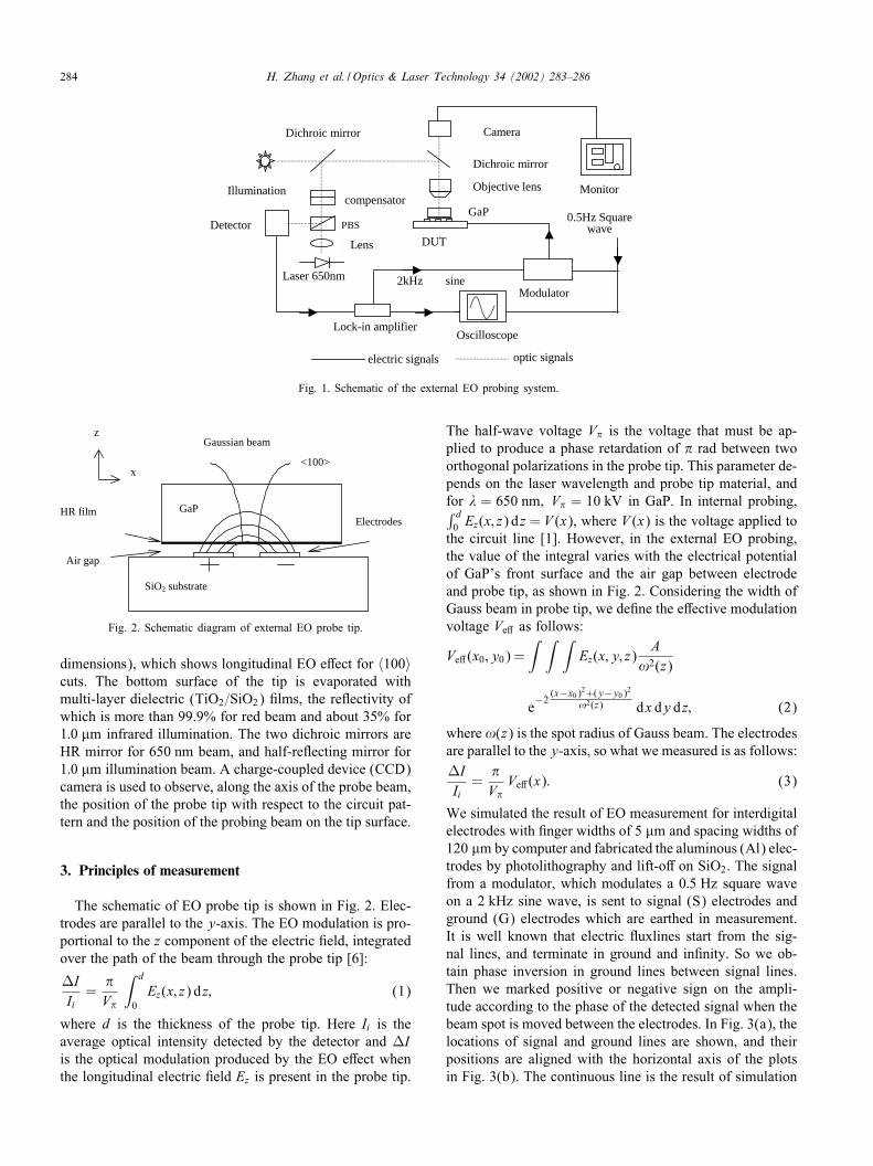
Fig. 2. Schematic diagram of external EO probe tip.
dimensions), which shows longitudinal EO e<ect for 〈100〉cuts. The bottom surface of the tip is evaporated withmulti-layer dielectric (TiO2=SiO2) :lms, the reEectivity ofwhich is more than 99.9% for red beam and about 35% for1:0 �m infrared illumination. The two dichroic mirrors areHR mirror for 650 nm beam, and half-reEecting mirror for1:0 �m illumination beam. A charge-coupled device (CCD)camera is used to observe, along the axis of the probe beam,the position of the probe tip with respect to the circuit pat-tern and the position of the probing beam on the tip surface.
3. Principles of measurement
The schematic of EO probe tip is shown in Fig. 2. Elec-trodes are parallel to the y-axis. The EO modulation is pro-portional to the z component of the electric :eld, integratedover the path of the beam through the probe tip [6]:
NIIi
=V
∫ d
0Ez(x; z) dz; (1)
where d is the thickness of the probe tip. Here Ii is theaverage optical intensity detected by the detector and NIis the optical modulation produced by the EO e<ect whenthe longitudinal electric :eld Ez is present in the probe tip.
The half-wave voltage V is the voltage that must be ap-plied to produce a phase retardation of rad between twoorthogonal polarizations in the probe tip. This parameter de-pends on the laser wavelength and probe tip material, andfor � = 650 nm; V = 10 kV in GaP. In internal probing,∫ d
0 Ez(x; z) dz = V (x), where V (x) is the voltage applied tothe circuit line [1]. However, in the external EO probing,the value of the integral varies with the electrical potentialof GaP’s front surface and the air gap between electrodeand probe tip, as shown in Fig. 2. Considering the width ofGauss beam in probe tip, we de:ne the e<ective modulationvoltage Ve< as follows:
Ve< (x0; y0) =∫ ∫ ∫
Ez(x; y; z)A
!2(z)
e−2
(x−x0)2+(y−y0)2
!2(z) dx dy dz; (2)
where !(z) is the spot radius of Gauss beam. The electrodesare parallel to the y-axis, so what we measured is as follows:NIIi
=VVe< (x): (3)
We simulated the result of EO measurement for interdigitalelectrodes with :nger widths of 5 �m and spacing widths of120 �m by computer and fabricated the aluminous (Al) elec-trodes by photolithography and lift-o< on SiO2. The signalfrom a modulator, which modulates a 0:5 Hz square waveon a 2 kHz sine wave, is sent to signal (S) electrodes andground (G) electrodes which are earthed in measurement.It is well known that electric Euxlines start from the sig-nal lines, and terminate in ground and in:nity. So we ob-tain phase inversion in ground lines between signal lines.Then we marked positive or negative sign on the ampli-tude according to the phase of the detected signal when thebeam spot is moved between the electrodes. In Fig. 3(a), thelocations of signal and ground lines are shown, and theirpositions are aligned with the horizontal axis of the plotsin Fig. 3(b). The continuous line is the result of simulation

H. Zhang et al. / Optics & Laser Technology 34 (2002) 283–286 285
Probe location(microns)
Vef
f(v)
(a) S
G
0 200 400 600 800 100 0-6
-4
-2
0
2
4
6
8
(b)
Fig. 3. Measurement and simulation of interdigital electrodes.
and squares denote the experimental result. From Fig. 3(b)we can see that positive and negative maximum values oc-cur on the signal and ground lines, respectively, and zeropoints occur between signal and ground lines. It is remark-able that negative maximum signals instead of zero occuron the ground lines and zero points occur between signaland ground lines. It should be zero on ground lines in inter-nal EO probing [1]. The inequality of the voltage detectedon signal and ground lines indicates that a few electric Eux-lines terminate in in:nite distance. The result indicated thatwhat we detected in external EO probing is not the electricpotential of the line under test, but Ve< , which is related tothe shape of electrodes, the thickness of the probe tip andthe air gap. Later, we will use this fact to measure the spatialresolution of the external EO probing equipment.
4. Spatial resolution
From classical optics, we know that when a well-extendedGauss beam passes through an objective lens, the diameterof di<raction spot of Gauss beam d, is given by
d=2�
√1 − NA2
NA(4)
where NA is the numerical aperture of the objective lens and� is the wavelength of the beam. Here �= 0:65 �m; NA =0:65, so d=0:48 �m. But the diameter of the di<raction spotis not the spatial resolution of the external EO probing [7].We de:ne the spatial resolution of external EO probing asthe minimum distance under detectable change of Ve< . Wefabricated and measured some samples with two Al elec-trodes on SiO2 substrate with a width of 3 �m and a spacingof 2 �m as shown in Fig. 5(a). We added another modula-tor and an inverter to guarantee the amplitude of Ez abovetwo electrodes to be equal, while the direction is reversed
To electrode B
2kHz sine wave 0.5Hz square wave
To electrode A
Modulator
Inverter
Modulator
Fig. 4. The schematic circuit diagram.
Probe Location microns
Vef
f(v)
0 1 2 3 4 5 6 7 8 9 10-1.5
-1.0
-0.5
0.0
0.5
1.0
1.5
B A
SiO2 substrate
Electrodes
(a)
(b)
Fig. 5. Measurement and simulation of electrodes with a spacing of 2 �m.
with each other. The schematic circuit diagram is shown inFig. 4. We located the center of the beam spot at the leftedge of electrode A, then moved the spot towards right ev-ery other 1 �m and measured it. The amplitude of the wave-form, which we can monitor in the oscilloscope, declinesgradually from 1:1 V with a positive phase. In the center ofthe two electrodes, the signal is submerged in noise voltage,which, we de:ne, is the noise voltage of the system. Thenthe amplitude increased gradually with a negative phase.Considering the noise voltage, we obtain a curve band. Theresult of the simulation and measurement is shown by acurve and mark, respectively, in Fig. 5. From Fig. 5 we cansee that the change of the measured signal near the centerof the two electrodes, caused by moving the beam spot inthe range of 0:5 �m, approximates to the noise voltage. Thisfact indicated that the spatial resolution of this EO probingequipment is at least ¡ 1 �m.
286 H. Zhang et al. / Optics & Laser Technology 34 (2002) 283–286
5. Voltage sensibility
The voltage sensibility of a measuring system is the volt-age of the test signal when signal-to-noise ratio approximatesto 1. When a 0:5 Hz square wave modulated by a 2 kHzsine wave was delivered into an indium–tin oxide coplanarstrip, the minimum detectable voltage 12:6 mV=
√Hz was
obtained.
6. Conclusion
In summary, a new electrical method is put forward todetermine the spatial resolution of external EO probing. Wesimulated the result of EO probing of some samples bycomputer and measured them with our external EO probingequipment. A spatial resolution of ¡ 1 �m and a voltagesensitivity of 12:6 mV=
√Hz have been obtained.
Acknowledgements
This work is supported by the National Science Foun-dation (69876014) of China and the National Key Lab ofASIC (JS02.3.1.JW1302).
References
[1] Bloom DM, et al. Electrooptic sampling in GaAs integrated circuits.IEEE J Quantum Electron 1986;QE22(1):79–93.
[2] Maobin Yi, et al. A practical electro-optic samplier for characterizationinternal to GaAs ICs. Int J High Speed Electron Systems1996;7(3):463–9.
[3] Kyoung Yang, et al. Electrooptic mapping and :nite-element modelingof the near-:eld pattern of a microstrip patch antenna. IEEE TransMicrowave Theory Techn 2000;48(2):288–94.
[4] Nagatsuma T, et al. Subpicosecond sampling using a noncontactelectro-optic probe. J Appl Phys 1989;66(9):4001–9.
[5] Mitsuru Shinagawa, et al. An automated electro-optic probing systemfor ultra-high-speed ICs. IEEE Trans Instrum Meas 1994;43(6):843–7.
[6] Heutmaker MS, Cook TB, Bosacchi B, et al. Electrooptic samplingof a packaged high-speed GaAs integrated circuit. IEEE J QuantumElectron 1988;24(2):226–33.
[7] David G, et al. Analysis of microwave propagation e<ects usingtwo-dimensional electrooptic :eld mapping techniques electronics.Opt Quantum Electron 1996;28:919–32.