Research Article Thin Film CIGS Solar Cells, Photovoltaic...
12
Hindawi Publishing Corporation International Journal of Photoenergy Volume 2013, Article ID 817424, 11 pages http://dx.doi.org/10.1155/2013/817424 Research Article Thin Film CIGS Solar Cells, Photovoltaic Modules, and the Problems of Modeling Antonino Parisi, Luciano Curcio, Vincenzo Rocca, Salvatore Stivala, Alfonso C. Cino, Alessandro C. Busacca, Giovanni Cipriani, Diego La Cascia, Vincenzo Di Dio, Rosario Miceli, and Giuseppe Ricco Galluzzo DEIM, University of Palermo, Viale delle Scienze, Building 9, 90128 Palermo, Italy Correspondence should be addressed to Rosario Miceli; [email protected] Received 13 July 2013; Accepted 13 August 2013 Academic Editor: Leonardo Palmisano Copyright © 2013 Antonino Parisi et al. is is an open access article distributed under the Creative Commons Attribution License, which permits unrestricted use, distribution, and reproduction in any medium, provided the original work is properly cited. Starting from the results regarding a nonvacuum technique to fabricate CIGS thin films for solar cells by means of single-step electrodeposition, we focus on the methodological problems of modeling at cell structure and photovoltaic module levels. As a matter of fact, electrodeposition is known as a practical alternative to costly vacuum-based technologies for semiconductor processing in the photovoltaic device sector, but it can lead to quite different structural and electrical properties. For this reason, a greater effort is required to ensure that the perspectives of the electrical engineer and the material scientist are given an opportunity for a closer comparison and a common language. Derived parameters from ongoing experiments have been used for simulation with the different approaches, in order to develop a set of tools which can be used to put together modeling both at single cell structure and complete module levels. 1. Introduction in film solar cells based on a compound of the elements Copper, Indium, Gallium, and Selenium, that is, CIGS semiconductors, are considered as highly promising light-to- electricity converters thanks to their direct bandgaps which can be efficiently matched to the solar spectrum [1]. Among different fabrication methods suitable for the absorber layer, electrodeposition represents an important alternative to the expensive vacuum-based technologies. Using a single-step electrodeposition, several groups have fabricated CIGS films [2], and in some case an efficiency exceeding 15% has been reported [3], not too far from top performances made pos- sible by the most studied vacuum-based three-stage process [1]. One of the most important requirements for successful application of the one-step electrodeposition here consid- ered, for CIGS film production, is to control composition of deposited films in a reliable and reproducible way (it is noteworthy that we found several technological requirements in common with optical applications we had previously developed in different research contexts, to which we address the reader [4–19]). Furthermore, film formation must be manufacturing friendly, possibly eliminating the selenization step, which is environmentally undesired due to the toxicity of Se. In some recent works [20, 21], we described our first results on the option to fabricate CIGS-based solar cells directly using electrodeposited films by adjusting the con- centration of the solution and eliminating the unwanted selenization step. Within the limits of the present discussion, it will be enough to mention that (1) electrodeposition of CIGS, with a controlled and reproducible Cu/(In +Ga) and Ga/(In +Ga) molar ratios, has been presented and (2) Cu-In- Se-Ga content and formation of secondary phases before and aſter the annealing process have been investigated [4, 6]. Also, in the context of our research project, it is required to derive parameters from ongoing experiments on the layered junction structures and use them for simulation with different approaches, in order to develop a set of tools which can be used to put together modeling both at single cell and module levels, what we will describe here. To complete the
Transcript of Research Article Thin Film CIGS Solar Cells, Photovoltaic...

Hindawi Publishing CorporationInternational Journal of PhotoenergyVolume 2013 Article ID 817424 11 pageshttpdxdoiorg1011552013817424
Research ArticleThin Film CIGS Solar Cells Photovoltaic Modules andthe Problems of Modeling
Antonino Parisi Luciano Curcio Vincenzo Rocca Salvatore StivalaAlfonso C Cino Alessandro C Busacca Giovanni Cipriani Diego La CasciaVincenzo Di Dio Rosario Miceli and Giuseppe Ricco Galluzzo
DEIM University of Palermo Viale delle Scienze Building 9 90128 Palermo Italy
Correspondence should be addressed to Rosario Miceli rosariomiceliunipait
Received 13 July 2013 Accepted 13 August 2013
Academic Editor Leonardo Palmisano
Copyright copy 2013 Antonino Parisi et alThis is an open access article distributed under the Creative CommonsAttribution Licensewhich permits unrestricted use distribution and reproduction in any medium provided the original work is properly cited
Starting from the results regarding a nonvacuum technique to fabricate CIGS thin films for solar cells by means of single-stepelectrodeposition we focus on the methodological problems of modeling at cell structure and photovoltaic module levels Asa matter of fact electrodeposition is known as a practical alternative to costly vacuum-based technologies for semiconductorprocessing in the photovoltaic device sector but it can lead to quite different structural and electrical properties For this reason agreater effort is required to ensure that the perspectives of the electrical engineer and thematerial scientist are given an opportunityfor a closer comparison and a common language Derived parameters from ongoing experiments have been used for simulationwith the different approaches in order to develop a set of tools which can be used to put together modeling both at single cellstructure and complete module levels
1 Introduction
Thin film solar cells based on a compound of the elementsCopper Indium Gallium and Selenium that is CIGSsemiconductors are considered as highly promising light-to-electricity converters thanks to their direct bandgaps whichcan be efficiently matched to the solar spectrum [1] Amongdifferent fabrication methods suitable for the absorber layerelectrodeposition represents an important alternative to theexpensive vacuum-based technologies Using a single-stepelectrodeposition several groups have fabricated CIGS films[2] and in some case an efficiency exceeding 15 has beenreported [3] not too far from top performances made pos-sible by the most studied vacuum-based three-stage process[1]
One of the most important requirements for successfulapplication of the one-step electrodeposition here consid-ered for CIGS film production is to control compositionof deposited films in a reliable and reproducible way (it isnoteworthy that we found several technological requirementsin common with optical applications we had previously
developed in different research contexts to which we addressthe reader [4ndash19])
Furthermore film formation must be manufacturingfriendly possibly eliminating the selenization step which isenvironmentally undesired due to the toxicity of Se
In some recent works [20 21] we described our firstresults on the option to fabricate CIGS-based solar cellsdirectly using electrodeposited films by adjusting the con-centration of the solution and eliminating the unwantedselenization step Within the limits of the present discussionit will be enough to mention that (1) electrodeposition ofCIGS with a controlled and reproducible Cu(In+Ga) andGa(In+Ga)molar ratios has been presented and (2) Cu-In-Se-Ga content and formation of secondary phases before andafter the annealing process have been investigated [4 6]
Also in the context of our research project it is requiredto derive parameters from ongoing experiments on thelayered junction structures and use them for simulation withdifferent approaches in order to develop a set of tools whichcan be used to put together modeling both at single cell andmodule levels what we will describe here To complete the
2 International Journal of Photoenergy
overall picture of the ongoing activity we will mention thatwe are adapting a previous sensor measurement setup tomapsolar cell performance with a light-beam-induced current(LBIC) configuration [22ndash24]
In particular from real data we have derived the five-parameter model and the complete characteristic of a CIGSmodule Afterwards from a structural model setting realCIGS cells parameters we have derived the cell characteristicA circuitalmodelmdashable to describe the cells interconnectionsand packagingmdashtook into account the simulated cells datahas been finally compared with the previously mentionedmodule simulation This comparison could be very useful todetermine the internal parameters that extend the structuralcells model to themodule characteristics so that the differentperspectives of the electrical engineer and the materialscientist are given an opportunity for a closer collaborationand a common language we are actively looking for [25]
Hence this paper is organized as follows In Section 2 wedescribe a general introduction tomodel simulationmethodsand the five-parameter analysis of a real CIGS moduleThen structural cell simulation is described in Section 3together with a parasitic network resistance modeling and acomparison with the module data Finally conclusions aredrawn in Section 4
2 Five Lumped Parameters Simulation
A photovoltaic (PV) module mathematical model is a veryuseful tool to evaluate electrical energy production during theoperative working of PV plants [26] Moreover such modelsare important to perform economic evaluations and comparedifferent PV plants implementations [27ndash30]
In the literature seldomparametricmathematicalmodelshave been proposed to simulate the solar cell functioningon the basis of distributed parameters equivalent circuitswhile lumped parameters equivalent circuits are largely morecommon [31ndash35] Among the lumped parameters modelsthere are different implementations that consider four fiveor six parameters with various threshold accuracies Modelparameters can be evaluated on the basis of the numericaldata from the manufacturers [31ndash34 36 37] Finally fittingmethods are used to match 119868-119881 characteristic curves withdifferent temperature and irradiance values
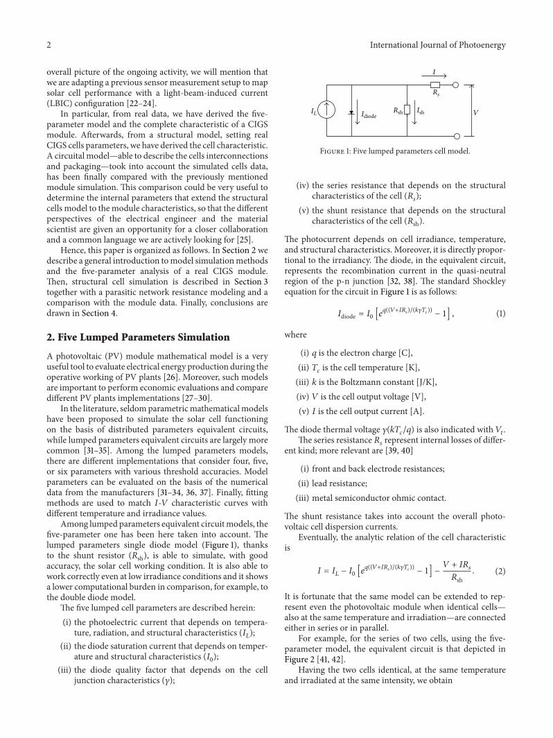
Among lumped parameters equivalent circuitmodels thefive-parameter one has been here taken into account Thelumped parameters single diode model (Figure 1) thanksto the shunt resistor (119877sh) is able to simulate with goodaccuracy the solar cell working condition It is also able towork correctly even at low irradiance conditions and it showsa lower computational burden in comparison for example tothe double diode model
The five lumped cell parameters are described herein(i) the photoelectric current that depends on tempera-
ture radiation and structural characteristics (119868119871)
(ii) the diode saturation current that depends on temper-ature and structural characteristics (119868
0)
(iii) the diode quality factor that depends on the celljunction characteristics (120574)
RshIdiodeIsh V
I
IL
Rs
Figure 1 Five lumped parameters cell model
(iv) the series resistance that depends on the structuralcharacteristics of the cell (119877
119904)
(v) the shunt resistance that depends on the structuralcharacteristics of the cell (119877sh)
The photocurrent depends on cell irradiance temperatureand structural characteristics Moreover it is directly propor-tional to the irradiancy The diode in the equivalent circuitrepresents the recombination current in the quasi-neutralregion of the p-n junction [32 38] The standard Shockleyequation for the circuit in Figure 1 is as follows
119868diode = 1198680 [119890119902((119881+119868119877
119904)(119896120574119879
119888))minus 1] (1)
where
(i) 119902 is the electron charge [C](ii) 119879119888is the cell temperature [K]
(iii) 119896 is the Boltzmann constant [JK](iv) 119881 is the cell output voltage [V](v) 119868 is the cell output current [A]
The diode thermal voltage 120574(119896119879119888119902) is also indicated with 119881
119905
The series resistance 119877119904represent internal losses of differ-
ent kind more relevant are [39 40]
(i) front and back electrode resistances(ii) lead resistance(iii) metal semiconductor ohmic contact
The shunt resistance takes into account the overall photo-voltaic cell dispersion currents
Eventually the analytic relation of the cell characteristicis
119868 = 119868119871minus 1198680[119890119902((119881+119868119877
119904)(119896120574119879
119888))minus 1] minus
119881 + 119868119877119904
119877sh (2)
It is fortunate that the same model can be extended to rep-resent even the photovoltaic module when identical cellsmdashalso at the same temperature and irradiationmdashare connectedeither in series or in parallel
For example for the series of two cells using the five-parameter model the equivalent circuit is that depicted inFigure 2 [41 42]
Having the two cells identical at the same temperatureand irradiated at the same intensity we obtain
International Journal of Photoenergy 3
Rsh2
Rsh1
Ish2
Ish1 V
V
1
V2
I
I
IL2
IL1
Cell 1
Cell 2
Idiode1
Idiode2
Rs1
Rs2
Figure 2 Equivalent circuit of the two cell series
Rsh
Rsh
Idiode Ish
I
IL
IL
V = V2
RsRs
Figure 3 Equivalent circuit of a two identical cell series
(i) 1198681198711= 1198681198712
(ii) 1198811= 1198812
(iii) 119868diode1 = 119868diode2 having the two identical diodes thesame working conditions
(iv) 1198771199041= 1198771199042
(v) 119877sh1 = 119877sh2(vi) 119868sh1 = 119868sh2
The aforementioned two cells scheme in the previoushypothesis is equivalent in the final analysis to the followingsimpler circuit of Figure 3 [41 43 44]
The extension to119873CS cells connected in series is obviousand the analytic relation for the module is then
119868 = 119868119871minus 1198680[119890119902((119881+119868119877
119904)119896120574119873CS119879119888) minus 1] minus
119881 + 119868119877119904
119877sh (3)
In order to evaluate the five-parameter values the methodhereafter reported has been adopted [33 45 46] Equation(3) is written by the three characteristic points maximumpower short-circuit and open-circuit points obtaining (4)(5) and (6) respectively Moreover the 119889119875119889119881 = 0 conditionby the maximum power point is derived giving (7) Finallythe fifth equation is obtained by calculating the 119889119868119889119881 valuecalculated in the short-circuit point which results in (8)
Equations (4) and (6) allow to evaluate 119868ref0
(9) Equations (9)and (5) are developed to build (10) where the three unknowns119877119904 119877sh and 119881119905 have to be evaluated Equation (10) together
with (7) and (8) allow to get (12) and (13)119877119904119877sh and119881119905 values
are determined from (10) (12) and (13) through the iterativemethod hereafter reported
119868refSC = 119868
ref119871minus 119868
ref0sdot 119890(119868
refSC119877119904)(119873CS119881119905) minus
119868refSC119877119904
119877sh (4)
119868refMP = 119868
ref119871minus 119868
ref0sdot 119890(119881
refMP+119868
refMP119877119904)(119873CS119881119905)
minus119881
refMP + 119868
refMP119877119904
119877sh
(5)
119868ref119871minus 119868
ref0sdot 119890(119881
refOC)(119873CS119881119905) minus
119881refOC119877sh
= 0 (6)
119889119875
119889119881
10038161003816100381610038161003816100381610038161003816119881=119881refMP 119868=119868refMP
= 119868refMP +
119889119868
119889119881
10038161003816100381610038161003816100381610038161003816119881=119881refMP 119868=119868refMP
119881refMP = 0 (7)
119889119868
119889119881
10038161003816100381610038161003816100381610038161003816119868=119868refSC
= minus1
119877sh (8)
119868ref0= (119868
refSC minus
119881refOC minus 119868
refSC119877119904
119877sh) sdot 119890minus(119881
refOC)(119873CS119881119905) (9)
119868refMP = 119868
refSC minus
119881refMP + 119868
refMP sdot 119877119904 minus 119868
refSC sdot 119877119904
119877sh
minus (119868refSC minus
119881refOC minus 119868
refSC sdot 119877119904
119877sh)119870119879
(10)
where
119870119879= 119890(119881
refMP+119868
refMP119877119904minus119881
refOC)(119873CS119881119905) (11)
119889119875
119889119881
10038161003816100381610038161003816100381610038161003816119881=119881refMP 119868=119868refMP
= 119868refMP
+ 119881refMP
sdot
minus(119868
refSC119877sh minus 119881
refOC + 119868
refSC119877119904)sdot119890
(119881refMP+119868
refMP119877119904minus119881
refOC)(119873CS119881119905)
119873CS119881119905119877shminus
1
119877sh
1 +(119868
refSC119877sh minus 119881
refOC + 119868
refSC119877119904) sdot 119890
(119881refMP+119868
refMP119877119904minus119881
refOC)(119873CS119881119905)
119873CS119881119905119877sh+119877119904
119877sh(12)
4 International Journal of Photoenergy
minus1
119877sh
10038161003816100381610038161003816100381610038161003816119868=119868refSC
=
minus(119868
refSC119877sh minus 119881
refOC + 119868
refSC119877119904) sdot 119890
(119868refSC119877119904minus119881
refOC)(119873CS119881119905)
119873CS119881119905119877shminus
1
119877sh
1 +(119868
refSC119877sh minus 119881
refOC + 119868
refSC119877119904) sdot 119890
(119868refSC119877119904minus119881
refOC)(119873CS119881119905)
119873CS119881119905119877sh+119877119904
119877sh
(13)
In the equations detailed previously standard test conditionsthat is STC are indicate with ldquoref rdquo as apex To summarizethe adopted iterative method a block diagram is traced inFigure 4 [46]
At the first stage the 119877119904and 119877sh starting values are
arbitrarily chosen and put into (10) in order to evaluate 119881119905
Subsequently (13) is used to evaluate 119877sh The new 119877sh valueis put into (12) in order to check the 119889119875119889119881 = 0 conditionIf 119889119875119889119881 = 0 the latter 119877sh value is the right one and (2)can be used to evaluate the 120574 form factor otherwise the119877sh initial value has to be changed and the iteration goeson The previously mentioned equations can be adopted inthat form only under standard conditions For this reasonit is necessary to take into account the changes of the 119868
0
119868119871 119868SC and 119881OC parameters with respect to temperature and
irradiation According to [46 47]
(i) 1198680does not depend on irradiation but only on temper-
ature(ii) 119868119871depends only on temperature
(iii) 119868SC depends both on temperature and irradiation(iv) 119881OC depends only on irradiation
The following equations describe what was stated previously
1198680 (119879) = (119868SC (119879) minus
119881OC (119879) minus 119868SC (119879) 119877119904119877sh
) sdot 119890minus119881OC(119879)(119873CS119881119905)
(14)
119881OC (119879) = 119881refOC + 120583119881OC
(119879119862minus 119879
ref119862) (15)
119868SC (119879) = 119868refSC [1 +
120583119868SC
100(119879119862minus 119879
ref119862)] (16)
119868SC (119866) = 119868refSC sdot
119866
119866ref (17)
119868119871(119866) = 119868
ref119871sdot119866
119866ref (18)
119868119871 (119866 119879) =
119866
119866ref sdot [1198680 (119879) sdot 119890119881OC(119879)(119873CS119881119905) +
119881OC (119879)
119877sh] (19)
119868SC (119866 119879) =119866
119866ref sdot 119868SC (119879)
=119866
119866ref sdot 119868refSC [1 +
120583119868SC
100(119879119862minus 119879
ref119862)]
(20)
where
(i) 120583119868SC
is the short-circuit current temperature coeffi-cient
(ii) 120583119881OC
is the open-circuit voltage temperature coeffi-cient
Therefore (14) (15) (19) and (20) represent the five-parameter mathematical model under changing temperatureand radiation conditions Finally the PV module outputvoltage can be expressed to good purpose by (21) derivedfrom (1)
119881 = [ln(119868119871 minus 1198681198680
+ 1 minus119881 + 119868119877
119904
1198680119877sh
)]119873CS119881119905 minus 119868119877119904 (21)
For example considering a commercial module with thefollowing nominal data
(i) 119868SC = 650A(ii) 119881OC = 468V(iii) 119868MP = 570A(iv) 119881MP = 344V(v) 120583119868SC= minus003K
(vi) 120583119881OC
= minus033K
the resulting five lumped parameter values are
(i) 120574 = 15(ii) 119877119904= 094Ω
(iii) 119877sh = 120Ω(iv) 119868119871= 66A
(v) 1198680= 37 sdot 10
minus7 A
In the following picture (Figure 5) the behavior of thecommercial module characteristic obtained from the five-parameter model in depicted which will be used later on fora paired comparison
3 The Structural Model from the Cell tothe Module
In parallel to the previously described approach usually thefirst choice for the electrical engineer it is worthwhile tofollow as well the microscopic point of view more familiarto the material scientist In order to generate a currentenergy derived from the sun must impact on a photovoltaicdevice having a preexisting electrical field such that freeelectrons can succeed in separating from holes Nowadaysnumerical simulation offers advantages to the design per-formance prediction and comprehension of the fundamentalphenomena ruling the operation of complex devices such assolar cells also allowing to investigate the physics of theirinner processes
Our tool of choice was wxAMPS a software capableof representing the electrical transport phenomena and theoptical response of a wide variety of layered structures like
International Journal of Photoenergy 5
Start
in short circuit point
True
True
Untrue
Untrue
End
Vt (Rs Rsh ) values from IMP equation
dPdV = 0 in MPP
dIdV = minus1Rsh
Rsh = (Rs Vt) calculation from dPdV equation
New Rsh value New Rsh value
Rs Rsh and Vt values setting
Rs Rsh and Vt final value
Figure 4 Determination of 119877119904 119877sh and 119881119905 block diagram
0 5 10 15 20 25 30 35 40 45 500
1
2
3
4
5
6
7
V module (V)
Im
odul
e (A
)
G = 1000Wm2
AM = 15
Tc = 29815K
Figure 5 119868-119881 curve from the five-parametermodel of a commercialPV module
those typical of solar cells For this reason it was alsoapplied to simulate the behavior of the solar cell discussed
in this work This software is an updated version rewrittenin C++ of the one-dimensional simulation programAnalysisof Microelectronic and Photonic Structures (AMPS-1D) thatwas initially developed by Fonash et al at PennsylvaniaState University [48 49] Various layers of stacked materialsproducing homojunctions heterojunctions and multijunc-tions can be studied by appropriately selecting characteristicparameters
Thus wxAMPS is a modern often updated solar cellsimulator for modeling one-dimensional devices composedof several materials It accepts the same input parametersas AMPS and is based on similar physical principles andnumerical descriptions of defects and recombinations [49]while adding tunnelling effects based on trap-assisted andintraband tunnelling models [50 51] This program incorpo-rates a new algorithm combining the Gummel and Newtonmethods In fact Gummelrsquos method alone is of limitedusefulness when simulating devices with very high defectdensities while Newtonrsquos method alone works poorly whendetermining intraband tunnelling current The advantagesof the combination are in terms of better stability andmore consistent convergence in problems in which intraband
6 International Journal of Photoenergy
tunnelling is critical in the determination of precise solutions[52]
With wxAMPS a hypothetically unlimited number oflayers can be modeled this added flexibility is suited totailoring designs of devices with parameters at any givendepth profile so as to establish optimal degrees of efficiencyconversions for solar cells The program allows data inputthrough three main windows that represent the ambient con-ditions the properties of differentmaterials for the individuallayers and the resolving model (trap-assisted tunnelling orintraband) You can use the simulation parameters providedby the University of Illinois Engineering Wiki [53] oryou can set custom data as needed Operating temperaturesolar spectrum quantum efficiency front and back contactdata surface recombination velocity and bias voltages arethe environmental parameters which set device workingconditions Once stored ambient conditions are defined forenvironment simulation but new settings can be edited byusers loading a properly tailored file In detail it is possible totake into account the values ofΦ
119861(the barrier height defined
as 119864119888minus 119864119891) for the front and back contacts and reflection
coefficients [54]Thematerial properties of each layer are divided into four
groups accessed by separate tabs electrical defect opticaland advanced A grid allows users to control and edit theoverall structure of the device Tables organize materialproperties and these are provided by a Wiki [53] website orare editable using common worksheets Likewise absorptioncoefficients can be edited directly by users or be loaded fromexternal data files
Once all required input is entered it is possible tostart data analysis The results are displayed by an efficientgraphical layout that presents them Output data can beprovided in two main forms directly through the graphicaluser interface or indirectly through files readable by commonspreadsheet programs
A CIGS thin film solar cell structure with parametersderived from our experiments was simulated after speci-fying as the input data the material parameters for eachindividual layer of the stacked device structures Specificallyseveral layers including the top contact bottom contactintrinsic ZnO layer CdS buffer layer high-recombinationinterface surface defect layer on top of the CIGS film andCIGS absorber defined the CIGS solar-cell structure Theemployed thicknesses of structural layers and the materialparameters which by the way fall into the acceptable rangesreported in the literature [55] are shown in Table 1
As usual room temperature and standard sunlight (AM15G) were the assumed working conditions Furthermorethe material parameters used in the simulations were keptunchanged Tables 2 and 3 summarize material Gaussiandefect states and contact parameters respectively Table 4provides an explanation of the symbols used in the previoustables The front and back contacts are solely defined by theirwork functionsΦ
119861
Considering that an accurate optical assessment of aphotovoltaic cell is hardly trivial in order to facilitate thediscussion and describe the considered simplifications wewill try to follow and illustrate reflections and absorptions to
Table 1 Simulationmaterial parameters of the CIGS thin-film solarcell
Parameter ZnO Al ZnO CdS CIGS119889 (120583m) 05 02 005 3120576119877
9 9 10 136119864119892(eV) 33 33 24 118
120594 (eV) 44 44 42 45119873119862[cmminus3] 22 sdot 10
1822 sdot 10
1822 sdot 10
1822 sdot 10
18
119873119881[cmminus3] 18 sdot 10
1918 sdot 10
1918 sdot 10
1918 sdot 10
19
120583119899[cm2(Vsdots)] 100 100 100 100
120583119901[cm2(Vsdots)] 25 25 25 25
119873119863[cmminus3] 1 sdot 10
181 sdot 107
11 sdot 1018 0
119873119860[cmminus3] 0 0 0 2 sdot 10
16
Table 2 Simulation material Gaussian defect for the CIGS solarlayers
Parameter ZnO Al ZnO CdS CIGSDefect type Donor Donor Acceptor DonorEnergy level [eV] 165 165 12 06Deviation [eV] 01 01 01 01120590119899[cm2] 1 times 10minus12 1 times 10minus12 1 times 10minus17 5 times 10minus13
120590119901[cm2] 1 times 10minus15 1 times 10minus15 1 times 10minus12 1 times 10minus15
119873119905[cmminus3] 1 times 1017 1 times 1017 1 times 1018 1 times 1014
Table 3 Contact parameters applied to the simulations
Parameter Back contact Front contact120601119861[eV] 066 0
119878119899[cms] 2 times 10
71 times 10
7
119878119901[cms] 2 times 10
71 times 10
7
Table 4 Explanation of the symbols used to describe the simulationparameters
Parameter Explanation119863 Layer thickness120576119877
Permittivity constant120594 Electron affinity
119873119862119873119881
Effective density of states in the conductionvalence band
120583119899120583119899
Mobility of electronsholes120590119899120590119901 Capture cross-section of electronsholes
119873119863119873119860
Doping concentration119873119905
Defect concentration120601119861
Potential barrier height119878119899119878119901 Surface recombination velocity of electronsholes
which photons from incident sunlight impacting on cells areexposed in their path
As illustrated in Figure 6 incident rays reflect at theair-glass (1) glass-encapsulant (3) and encapsulant-cell (5)interfaces In the latter case reflection is often diffuse leading
International Journal of Photoenergy 7
1
2
3
4
5
6
7
Glass
Encapsulant
CIGS cell
Molybdenum
Figure 6 Cross-sectional diagram of a conventional photovoltaicmodule (not in scale) and the optical loss as described in the text
0 01 02 03 04 05 06 070
5
10
15
20
25
30
V cell (V)
Ice
ll (m
Ac
m2)
Figure 7 119868-119881 curve (per cm2) a simulated CIGS solar cell
to some of the reflected light being totally internally reflectedat the glass-air interface remaining within the cell
Furthermore incident rays are absorbed by the glass(2) the encapsulant (4) and the cellrsquos antireflection coatingor metal fingers (6) In addition further losses arise fromincident rays within interspace between adjacent cells (7)
These seven interactions depend on the lightrsquos incidentwavelength and angle [56]
In order to take into account overall losses due toreflection and absorption we have set to 02 the reflectioncoefficient for light impinging on the uppermost surfaceInstead for the back surface the reflection coefficient was setto 09
As well known a CIGS solar cell presents a compositestructure and the study is difficult due to this stratified win-dow consisting of a thin Al doped ZnO layer an un-dopedZnO a CdS buffer layer (or using Cd-free buffer layers) Inorder to predict the behavior of solar cells with a complexstructure as in the case in analysis it is important to usespecific and detailed physical models which are implementedto the computer so that the effect of considered inputmaterialparameters can be defined and assessed quantitatively
Figure 7 shows the 119868-119881 characteristic (per cm2) calcu-lated using wxAMPS again of the CIGS solar cell structurehaving material parameters listed in Tables 1ndash4 at roomtemperature and standard sunlight (AM 15G)
IshIL Idiode Vcell
minus
+
IcellRs internal
Rsh internal
Figure 8 The one diode model for a p-n-junction solar cell
Now we will recall a brief qualitative description of the119868-119881 characteristic curve of a common solar cell In fact anormal 119868-119881 curve presents a smooth shape in which it ispossible to distinguish three distinct voltage regions firstabove 0V a slightly sloped region second below 119881OC asteeply sloped and in the region of the maximum powerpoint a ldquokneerdquo As shown in Figure 7 normally the threeregions are smooth and continuous but the position of theknee depends on cell technology andmanufacturer In detailcrystalline silicon cells show sharper knees whereas thin filmsolar cells have gradual knees The slopes of the curve in thefirst two regions are caused by parasitic effects
Truth be told several causes lead to the power dissipationin solar cells but among these the most important is powerdissipation due to parasitic resistances Figure 8 representsthe one diode equivalent circuit for a p-n-junction solar celland in this model solar cells are described as a currentgenerator in parallel with a diode and a shunt resistanceinternal 119877sh of cell which all are connected in series withanother resistance internal 119877
119904of cell 119868
119871is the photo-
generated current and 119868diode is the current within a p-n-junction solar cell diode whereas 119868sh and 119868cell are the currentsinto parasitic resistances (ie internal 119877sh and 119877
119904) In order
to design a performing solar cell internal 119877119904should be as low
as possible and 119877sh as high as possibleFor a typical CIGS cell formation of internal series
resistance (119877119904) of the cell is mainly due to a ZnOAl layer
film resistance (typically 15Ω◻) resistances of various celllayers and resistance of top and back contacts In particularthe contact resistance between CIGS absorber layer andMolybdenum (back contact) can be ohmic or junction-likedepending on type and CIGS doping level
It is assumable that in a common solar cell119877sh arises fromcurrent leakingwithin the cell in high-conducting paths crossthe p-n-junction or around the edges Shunt paths that ishigh-conducting paths within the material can be a resultof presence of the impurities or crystal damage during theproduction phases [57]
The simulation program wxAmps takes into accountoverall volume resistances and the two resistances of back andtop contact that arise in different device layers In particularFigure 7 shows 119868-119881 curve obtained from simulations withwxAmps This curve shows that the simulated cell has aninternal series resistance equal to 18 [Ω times cm2] and an inter-nal shunt resistance equal to 890 [Ω times cm2] respectively
In order to determine the electrical behaviour of themodule starting from individual cells other resistive contri-butions to those simply derivable from 119868-119881 characteristic of
8 International Journal of Photoenergy
Rs external Rs external Rs external
Rsh external Rsh external Rsh external
Vmodule
Imodule
Cell1 Cell2 CellN
minus+
Figure 9 Equivalent electrical scheme of module
Im
odul
e (A
)
V module (V)
7
6
5
4
3
2
1
00 5 10 15 20 25 30 40 45 5035
Rs external0mΩ
10mΩ
20mΩ
40mΩ
100mΩ
(a)
Im
odul
e (A
)
V module (V)
7
6
5
4
3
2
1
00 5 10 15 20 25 30 40 45 5035
Rsh external
100mΩ
5mΩ
1mΩ
05mΩ
(b)
Figure 10 Effects of parasitic resistance on the simulated 119868-119881characteristics of 230 cm2 CIGS solar cell (a) Increasing externalseries resistance (b) Increasing external shunt resistance
elementary cell must be added sheet resistance of ZnOAlgrid contributions and interconnection resistance betweenmodule cells (ie metallic interconnections and contacts)[58]
Such contributions shall be considered separately becausewxAmps is a one-dimensional simulator and devicersquos cross-sectional dimensions and interconnections between cells areneglected Similarly we must also consider additional shuntresistance of overall module mainly due to the fact thatshunt paths exist in photovoltaic solar cell interconnects andmodule 119868sc mismatch
In detail this additional shunt resistance is due to defectsin materials or degradation of interconnections between cellsmonolithically integrated in amodule Dielectric material in-homogeneities and defects in thin-film solar cells or crystaldamage that can produce a variation of the shunt resistanceextending to cells (shunt currents through the p-n junction)have been observed experimentally [59] Unintentional par-tial shorting of cell near edges can cause a highly ohmic shuntpath for example connection between front-front and theback-back contacts of all cells Shunt currents between thefront and back contacts of cells are other possible causes
The set of all these additional resistances are simplifiedconsidering electrical model of Figure 9 obtained addingthe resistors 119877sh external and 119877s external The electric model wasproperly evaluated to switch from single cell to completemodule The module considered in our study consists of 72cells in series and each having an area of around 230 cm2
This step complicates the discussion by introducing (aswe have seen) a network of parasitic resistances
If 119877sh external and 119877s external are taken into account accord-ing to scheme in Figure 9 119868-119881 equation of module can bewritten as a function of single cell
119868mod =119877sh external lowast 119868cell
119877sh external + (119877sh external2)
minus119881mod 119873
119877shexternal + (119877shexternal2)
(22)
119877s external and 119877sh external are detrimental to solar cell andmodule performance in fact both reduce fill factor as isillustrated in Figures 10(a) and 10(b)
The current 119868sh leaking through the 119877sh of moduledecreases current output 119868module to intended load Thesmaller 119877sh the greater 119868sh and lower 119868module for a givenvoltageV A very low 119877sh reduces119881OC but does not affect 119868sh119877119904gives rise to a potential drop which reduces the voltage
output V but leaves 119881OC unaffected whereas a very high 119877119904
reduces 119868SC
International Journal of Photoenergy 9I
mod
ule (
A)
V module (V)
7
6
5
4
3
2
1
00 5 10 15 20 25 30 40 45 5035
G = 1000Wm2
AM = 15
Tc = 29815K
I-V five lumped parameters moduleI-V structural simulated module
Figure 11 119868-119881 curve from the five parameter model and structuralmodel with parasitic resistances
4 Comparison of Models and Conclusions
From the comparison of the five lumped parameters andthe structural model of a PV commercial module we haveextracted the values of the local parasitic network resistancesto be associated with the structural simulation Figure 11shows the good agreement which can be obtained betweenthe two models
Further refinements are required but we think that theapproach and methods here described can lead to the devel-opment of an important tool to evaluate intermediate resultsduring CIGS cell technology development and assessment ofits impact on global electrical module performance
This is particularly useful in the course of a researchactivity which encompasses a variety of contributions fromtechnical subjects such as electrochemistry semiconductorscience electrical and electronic engineering and opticalmeasurements We are trying to keep as linked as possibleduring the task of modeling both the level of single cellstructure and that of the complete photovoltaic module Inother words it is our way to look actively for a commonlanguage so that the different perspectives of the electricalengineer and the material scientist are given an opportunityfor a closer collaboration
We are currently applying this approach to the fabricationof thin filmCIGS solar cells bymeans of single-step electrode-position a technique which appears fairly easy and low costbut at the same time can lead to quite different structuraland electrical properties so that a reasonable estimation ofits impact on module characteristics is required in all theintermediate steps of our project
Conflict of Interests
Professor Rosario Miceli declares the following ldquoMATLABrdquoand ldquoSIMULINKrdquo are registered trademarks of The Math-Works Inc ldquowxAMPSrdquo is a freeware software made available
by the University of Illinois at Urbana-Champaign (UIUC)in collaboration with Nankai University of China In bothcases all the authors do not have any conflict of interests withthe content of the paper
Acknowledgments
The activity described previously has been supported bythe PON 01 1725 ldquoNuove tecnologie fotovoltaiche per sis-temi intelligenti integrati in Edificirdquo and the PON 02 00355ldquoTecnologie per lrsquoENERGia e lrsquoEfficienza energETICamdashENERGETICrdquo Research Programs Contributions came alsofrom SDESLab University of Palermo Finally the authorsexpress their gratitude to Professor Rockett Yiming Liu andProfessor Fonash for making freely available their simulationsoftware wxAMPS
References
[1] T Unold and C A Kaufmann ldquo118-chalcopyrite thin-filmmaterials and solar cellsrdquo in Comprehensive Renewable EnergyE C A Sayigh Ed pp 399ndash422 Elsevier Oxford UK 2012
[2] V S Saji I-H Choi and C-W Lee ldquoProgress in electrode-posited absorber layer for CuIn
1minus119909Ga119909Se2(CIGS) solar cellsrdquo
Solar Energy vol 85 no 11 pp 2666ndash2678 2011[3] R N Bhattacharya W Batchelor J F Hiltner and J R Sites
ldquoThin-film Culn1minus119909
Ga119909Se2photovoltaic cells from solution-
based precursor layersrdquo Applied Physics Letters vol 75 no 10pp 1431ndash1433 1999
[4] A C Busacca A C Cino S Riva-Sanseverino M Ravaro andG Assanto ldquoSilicamasks for improved surface poling of lithiumniobaterdquo Electronics Letters vol 41 no 2 pp 92ndash94 2005
[5] A C Busacca E DrsquoAsaro A Pasquazi S Stivala and GAssanto ldquoUltraviolet generation in periodically poled lithiumtantalate waveguidesrdquo Applied Physics Letters vol 93 no 12Article ID 121117 2008
[6] A C Busacca C A Santini S R Sanseverino et al ldquoSurfaceperiodic poling in congruent lithium tantalaterdquo ElectronicsLetters vol 42 no 9 pp 546ndash547 2006
[7] A C Busacca C L Sones R W Eason and S MailisldquoFirst-order quasi-phase-matched blue light generation insurface-poled Tiindiffused lithium niobate waveguidesrdquoApplied Physics Letters vol 84 no 22 pp 4430ndash4432 2004
[8] A C Busacca S Stivala L Curcio and G Assanto ldquoParametricconversion in micrometer and submicrometer structured fer-roelectric crystals by surface polingrdquo International Journal ofOptics vol 2012 Article ID 606892 11 pages 2012
[9] A C Busacca S Stivala L Curcio and P Livreri ldquoRandomquasi-phase matching in congruent lithium tantalate waveg-uides by proton exchangerdquo Electronics Letters vol 48 pp 783ndash784 2012
[10] E Cantelar M Domenech G Lifante et al ldquoMulti-line NIR-RGB emission in NdLiNbO
3RPE optical waveguidesrdquo Elec-
tronics Letters vol 43 no 11 pp 632ndash633 2007[11] E Cantelar G Lifante F Cusso et al ldquoDual-polarization-
pumpCW laser operation in Nd3+LiNbO3channel waveguides
fabricated by reverse proton exchangerdquo Optical Materials vol30 no 7 pp 1039ndash1043 2008
[12] M Cherchi S Bivona A C Cino A C Busacca and RL Oliveri ldquoUniversal charts for optical difference frequency
10 International Journal of Photoenergy
generation in the terahertz domainrdquo IEEE Journal of QuantumElectronics vol 46 no 6 pp 1009ndash1013 2010
[13] M Cherchi S Stivala A Pasquazi et al ldquoSecond-harmonicgeneration in surface periodically poled lithium niobate waveg-uides on the role ofmultiphoton absorptionrdquoApplied Physics Bvol 93 no 2-3 pp 559ndash565 2008
[14] M Cherchi A Taormina A C Busacca et al ldquoExploiting theoptical quadratic nonlinearity of zinc-blende semiconductorsfor guided-wave terahertz generation a material comparisonrdquoIEEE Journal of QuantumElectronics vol 46 no 3 pp 368ndash3762010
[15] M Clerici L Caspani E Rubino et al ldquoCounterpropagatingfrequency mixing with terahertz waves in diamondrdquo OpticsLetters vol 38 pp 178ndash180 2013
[16] G Nava P Minzioni I Cristiani et al ldquoIntegrated frequencyshifter in periodically poled lithium tantalate waveguiderdquo Elec-tronics Letters vol 46 no 25 pp 1686ndash1688 2010
[17] A Pasquazi A Busacca S Stivala R Morandotti and GAssanto ldquoNonlinear disorder mapping through three-wavemixingrdquo IEEE Photonics Journal vol 2 no 1 2010
[18] E M Rodrıguez D Jaque E Cantelar et al ldquoTime resolvedconfocal luminescence investigations on Reverse ProtonExchange NdLiNbO
3channel waveguidesrdquoOptics Express vol
15 no 14 pp 8805ndash8811 2007[19] S Stivala A Pazquazi L Colace et al ldquoGuided-wave frequency
doubling in surface periodically poled lithium niobate compet-ing effectsrdquo Journal of the Optical Society of America B vol 24no 7 pp 1564ndash1570 2007
[20] R Inguanta S Piazza C Sunseri et al ldquoAn electrochemicalroute towards the fabrication of nanostructured semiconductorsolar cellsrdquo in Proceedings of the International Symposium onPower Electronics Electrical Drives Automation and Motion(SPEEDAM rsquo10) pp 1166ndash1171 June 2010
[21] R L Oliveri R Inguanta T Spano et al ldquoCIGS thin film byone-step electrodeposition for solar cellsrdquo in Proceedings of 15thItalian National Conference of Photonic Technologies (Fotonicarsquo13) Milan Italy 2013
[22] A Parisi A C Cino A C Busacca M Cherchi and SRiva-Sanseverino ldquoIntegrated optic surface plasmon resonancemeasurements in a borosilicate glass substraterdquo Sensors vol 8no 11 pp 7113ndash7124 2008
[23] A Parisi F P DrsquoAleo S Guarino et al ldquoIntegrated opticsurface plasmon resonance measurements in glass substratesrdquoin Proceedings of the 3rd European Workshop on Optical FibreSensors vol 6619 of Proceedings of SPIE Napoli Italy July 2007
[24] S Stivala A Pasquazi A C Busacca et al ldquoFrequency dou-bling in surface periodically poled lithium niobate waveguidescompeting effectsrdquo in Proceedings of the European Conferenceon Lasers and Electro-Optics and the International QuantumElectronics Conference (CLEOE-IQEC rsquo07) Munich Germany2007
[25] A Parisi L Curcio V Rocca et al ldquoPhotovoltaic modulecharacteristics from CIGS solar cell modellingrdquo in Proceedingsof the International Conference Renewable Energy Research andApplications (ICRERA rsquo13) 2013
[26] R Miceli ldquoEnergy management and smart gridsrdquo Energies vol6 pp 2262ndash2290 2013
[27] G Cipriani V Di Dio D La Manna F Massaro R Miceli andG Zizzo ldquoEconomic analysis on dynamic photovoltaic systemsin new italian ldquofeed in tariffsrdquo contextrdquo in Proceedings of theInternational Conference on Clean Electrical Power RenewableEnergy Resources Impact (ICCEPrsquo13) 2013
[28] G Cipriani V Di Dio L P Di Noia et al ldquoA PV plantsimulator for testing MPPT techniquesrdquo in Proceedings of theInternational Conference on Clean Electrical Power RenewableEnergy Resources Impact (ICCEP rsquo13) 2013
[29] V Di Dio S Favuzza D La Caseia and R Miceli ldquoEconomicalincentives and systems of certification for the production ofelectrical energy from renewable energy resourcesrdquo in Proceed-ings of the International Conference on Clean Electrical Power(ICCEP rsquo07) pp 277ndash282 May 2007
[30] V Di Dio R Miceli C Rando and G Zizzo ldquoDynam-ics photovoltaic generators technical aspects and economicalvaluationrdquo in Proceedings of the International Symposium onPower Electronics Electrical Drives Automation and Motion(SPEEDAM rsquo10) pp 635ndash640 June 2010
[31] M Bouzguenda T Salmi A Gastli and A Masmoudi ldquoEvalu-ating solar photovoltaic system performance using MATLABrdquoin Proceedings of the 1st International Conference on RenewableEnergies and Vehicular Technology (REVET rsquo12) pp 55mdash559
[32] A N Celik and N Acikgoz ldquoModelling and experimentalverification of the operating current of mono-crystalline pho-tovoltaic modules using four- and five-parameter modelsrdquoApplied Energy vol 84 no 1 pp 1ndash15 2007
[33] G Cipriani V Di Dio D La Cascia R Miceli and R Rizzo ldquoAnovel approach for parameters determination in four lumpedPV parametric model with operative range evaluationsrdquo Inter-national Review of Electrical Engineering vol 8 2013
[34] G Farivar and B Asaei ldquoPhotovoltaic module single diodemodel parameters extraction based on manufacturer datasheetparametersrdquo in Proceedings of the IEEE International Conferenceon Power and Energy (PECon rsquo10) pp 929ndash934 December 2010
[35] M G Villalva J R Gazoli and E R Filho ldquoComprehensiveapproach to modeling and simulation of photovoltaic arraysrdquoIEEE Transactions on Power Electronics vol 24 no 5 pp 1198ndash1208 2009
[36] G Cipriani G Ciulla V Di Dio D La Cascia and R MicelildquoA device for PV modules I-V characteristic detectionrdquo inProceedings of the International Conference on Clean ElectricalPower Renewable Energy Resources Impact (ICCEP rsquo13) 2013
[37] V Lo Brano AOrioli G Ciulla andADiGangi ldquoAn improvedfive-parameter model for photovoltaic modulesrdquo Solar EnergyMaterials and Solar Cells vol 94 no 8 pp 1358ndash1370 2010
[38] A Luque and S Egedus Handbook of Photovoltaic Science andEngineering Wiley Chichester UK 2003
[39] F Ghani M Duke and J Carson ldquoNumerical calculation ofseries and shunt resistance of a photovoltaic cell using theLambert W-function experimental evaluationrdquo Solar Energyvol 87 pp 246ndash253 2013
[40] M A Green Solar Cells Operating Principles Technology andSystem Applications vol 1 Prentice Hall Upper Saddle RiverNJ USA 1982
[41] A Chatterjee A Keyhani and D Kapoor ldquoIdentification ofphotovoltaic source modelsrdquo IEEE Transactions on EnergyConversion vol 26 no 3 pp 883ndash889 2011
[42] S Li and H Zheng ldquoEnergy extraction characteristic study ofsolar photovoltaic cells andmodulesrdquo in Proceedings of the IEEEPower and Energy Society General MeetingThe Electrification ofTransportation and theGrid of the Future SanDiegoCalif USAJuly 2011
[43] H -L Tsai C S Tu and Y J Su ldquoDevelopment of generalizedphotovoltaic model using MATLABSIMULINKrdquo in Proceed-ings of theWorld Congress on Engineering and Computer ScienceWCECS (rsquo08) San Francisco Calif USA 2008
International Journal of Photoenergy 11
[44] MG Villalva J R Gazoli and E Ruppert Filho ldquoModeling andcircuit-based simulation of photovoltaic arraysrdquo in Proceedingsof the Brazilian Power Electronics Conference (COBEP rsquo09) pp1244ndash1254 Bonito-Mato Grosso do Sul Brazil October 2009
[45] W De Soto S A Klein andW A Beckman ldquoImprovement andvalidation of amodel for photovoltaic array performancerdquo SolarEnergy vol 80 no 1 pp 78ndash88 2006
[46] D Sera R Teodorescu and P Rodriguez ldquoPV panel modelbased on datasheet valuesrdquo in Proceedings of the IEEE Interna-tional Symposium on Industrial Electronics (ISIE rsquo07) pp 2392ndash2396 Vigo Spain June 2007
[47] V Di Dio D La Cascia R Miceli and C Rando ldquoA mathe-matical model to determine the electrical energy production inphotovoltaic fields under mismatch effectrdquo in Proceedings of theInternational Conference on Clean Electrical Power (ICCEP rsquo09)pp 46ndash51 Capri Italy June 2009
[48] H Zhu A K Kalkan J Hou and S J Fonash ldquoApplications ofAMPS-1D for solar cell simulationrdquoAIPConference Proceedingsvol 462 pp 309ndash314 1999
[49] S Fonash J Arch J Cuiffi et al et al ldquoA manual for AMPS-1D for Windows 95NTrdquoThe Pennsylvania State University pp10ndash31 1997
[50] G A M Hurkx D B M Klaassen and M P G KnuversldquoA new recombination model for device simulation includingtunnelingrdquo IEEE Transactions on Electron Devices vol 39 no 2pp 331ndash338 1992
[51] K Yang J R East and G I Haddad ldquoNumerical modelingof abrupt heterojunctions using a thermionic-field emissionboundary conditionrdquo Solid-State Electronics vol 36 no 3 pp321ndash330 1993
[52] Y Liu Y Sun and A Rockett ldquoAn improved algorithm forsolving equations for intra-band tunneling current in hetero-junction solar cellsrdquoThin Solid Films vol 520 no 15 pp 4947ndash4950 2012
[53] httpswikiengrillinoisedudisplaysolarcellsim[54] Y Liu Y Sun and A Rockett ldquoA new simulation software of
solar cellsmdashwxAMPSrdquo Solar Energy Materials and Solar Cellsvol 98 pp 124ndash128 2012
[55] M Gloeckler A L Fahrenbruch and J R Sites ldquoNumericalmodeling of CIGS and CdTe solar cells setting the baselinerdquo inProceedings of the 3rd World Conference on Photovoltaic EnergyConversion vol 1 pp 491ndash494 Osaka Japan May 2003
[56] K R McIntosh J N Cotsell J S Cumpston A W Norris NE Powell and B M Ketola ldquoAn optical comparison of siliconeand eva encapsulants for conventional silicon PV modules aray-tracing studyrdquo in Proceedings of the 34th IEEE PhotovoltaicSpecialists Conference (PVSC rsquo09) pp 544ndash549 PhiladelphiaPa USA June 2009
[57] E E van Dyk and E L Meyer ldquoAnalysis of the effect of para-sitic resistances on the performance of photovoltaic modulesrdquoRenewable Energy vol 29 no 3 pp 333ndash344 2004
[58] M A Green Solar Cells Operating Principles Technology andSystem Applications vol 1 of Prentice-Hall Series in Solid statePhysical Electronics Prentice Hall New York NY USA 1982
[59] U Malm and M Edoff ldquoSimulating material inhomogeneitiesand defects in CIGS thin-film solar cellsrdquo Progress in Photo-voltaics vol 17 no 5 pp 306ndash314 2009
Submit your manuscripts athttpwwwhindawicom
Hindawi Publishing Corporationhttpwwwhindawicom Volume 2014
Inorganic ChemistryInternational Journal of
Hindawi Publishing Corporation httpwwwhindawicom Volume 2014
International Journal ofPhotoenergy
Hindawi Publishing Corporationhttpwwwhindawicom Volume 2014
Carbohydrate Chemistry
International Journal of
Hindawi Publishing Corporationhttpwwwhindawicom Volume 2014
Journal of
Chemistry
Hindawi Publishing Corporationhttpwwwhindawicom Volume 2014
Advances in
Physical Chemistry
Hindawi Publishing Corporationhttpwwwhindawicom
Analytical Methods in Chemistry
Journal of
Volume 2014
Bioinorganic Chemistry and ApplicationsHindawi Publishing Corporationhttpwwwhindawicom Volume 2014
SpectroscopyInternational Journal of
Hindawi Publishing Corporationhttpwwwhindawicom Volume 2014
The Scientific World JournalHindawi Publishing Corporation httpwwwhindawicom Volume 2014
Medicinal ChemistryInternational Journal of
Hindawi Publishing Corporationhttpwwwhindawicom Volume 2014
Chromatography Research International
Hindawi Publishing Corporationhttpwwwhindawicom Volume 2014
Applied ChemistryJournal of
Hindawi Publishing Corporationhttpwwwhindawicom Volume 2014
Hindawi Publishing Corporationhttpwwwhindawicom Volume 2014
Theoretical ChemistryJournal of
Hindawi Publishing Corporationhttpwwwhindawicom Volume 2014
Journal of
Spectroscopy
Analytical ChemistryInternational Journal of
Hindawi Publishing Corporationhttpwwwhindawicom Volume 2014
Journal of
Hindawi Publishing Corporationhttpwwwhindawicom Volume 2014
Quantum Chemistry
Hindawi Publishing Corporationhttpwwwhindawicom Volume 2014
Organic Chemistry International
ElectrochemistryInternational Journal of
Hindawi Publishing Corporation httpwwwhindawicom Volume 2014
Hindawi Publishing Corporationhttpwwwhindawicom Volume 2014
CatalystsJournal of
2 International Journal of Photoenergy
overall picture of the ongoing activity we will mention thatwe are adapting a previous sensor measurement setup tomapsolar cell performance with a light-beam-induced current(LBIC) configuration [22ndash24]
In particular from real data we have derived the five-parameter model and the complete characteristic of a CIGSmodule Afterwards from a structural model setting realCIGS cells parameters we have derived the cell characteristicA circuitalmodelmdashable to describe the cells interconnectionsand packagingmdashtook into account the simulated cells datahas been finally compared with the previously mentionedmodule simulation This comparison could be very useful todetermine the internal parameters that extend the structuralcells model to themodule characteristics so that the differentperspectives of the electrical engineer and the materialscientist are given an opportunity for a closer collaborationand a common language we are actively looking for [25]
Hence this paper is organized as follows In Section 2 wedescribe a general introduction tomodel simulationmethodsand the five-parameter analysis of a real CIGS moduleThen structural cell simulation is described in Section 3together with a parasitic network resistance modeling and acomparison with the module data Finally conclusions aredrawn in Section 4
2 Five Lumped Parameters Simulation
A photovoltaic (PV) module mathematical model is a veryuseful tool to evaluate electrical energy production during theoperative working of PV plants [26] Moreover such modelsare important to perform economic evaluations and comparedifferent PV plants implementations [27ndash30]
In the literature seldomparametricmathematicalmodelshave been proposed to simulate the solar cell functioningon the basis of distributed parameters equivalent circuitswhile lumped parameters equivalent circuits are largely morecommon [31ndash35] Among the lumped parameters modelsthere are different implementations that consider four fiveor six parameters with various threshold accuracies Modelparameters can be evaluated on the basis of the numericaldata from the manufacturers [31ndash34 36 37] Finally fittingmethods are used to match 119868-119881 characteristic curves withdifferent temperature and irradiance values
Among lumped parameters equivalent circuitmodels thefive-parameter one has been here taken into account Thelumped parameters single diode model (Figure 1) thanksto the shunt resistor (119877sh) is able to simulate with goodaccuracy the solar cell working condition It is also able towork correctly even at low irradiance conditions and it showsa lower computational burden in comparison for example tothe double diode model
The five lumped cell parameters are described herein(i) the photoelectric current that depends on tempera-
ture radiation and structural characteristics (119868119871)
(ii) the diode saturation current that depends on temper-ature and structural characteristics (119868
0)
(iii) the diode quality factor that depends on the celljunction characteristics (120574)
RshIdiodeIsh V
I
IL
Rs
Figure 1 Five lumped parameters cell model
(iv) the series resistance that depends on the structuralcharacteristics of the cell (119877
119904)
(v) the shunt resistance that depends on the structuralcharacteristics of the cell (119877sh)
The photocurrent depends on cell irradiance temperatureand structural characteristics Moreover it is directly propor-tional to the irradiancy The diode in the equivalent circuitrepresents the recombination current in the quasi-neutralregion of the p-n junction [32 38] The standard Shockleyequation for the circuit in Figure 1 is as follows
119868diode = 1198680 [119890119902((119881+119868119877
119904)(119896120574119879
119888))minus 1] (1)
where
(i) 119902 is the electron charge [C](ii) 119879119888is the cell temperature [K]
(iii) 119896 is the Boltzmann constant [JK](iv) 119881 is the cell output voltage [V](v) 119868 is the cell output current [A]
The diode thermal voltage 120574(119896119879119888119902) is also indicated with 119881
119905
The series resistance 119877119904represent internal losses of differ-
ent kind more relevant are [39 40]
(i) front and back electrode resistances(ii) lead resistance(iii) metal semiconductor ohmic contact
The shunt resistance takes into account the overall photo-voltaic cell dispersion currents
Eventually the analytic relation of the cell characteristicis
119868 = 119868119871minus 1198680[119890119902((119881+119868119877
119904)(119896120574119879
119888))minus 1] minus
119881 + 119868119877119904
119877sh (2)
It is fortunate that the same model can be extended to rep-resent even the photovoltaic module when identical cellsmdashalso at the same temperature and irradiationmdashare connectedeither in series or in parallel
For example for the series of two cells using the five-parameter model the equivalent circuit is that depicted inFigure 2 [41 42]
Having the two cells identical at the same temperatureand irradiated at the same intensity we obtain
International Journal of Photoenergy 3
Rsh2
Rsh1
Ish2
Ish1 V
V
1
V2
I
I
IL2
IL1
Cell 1
Cell 2
Idiode1
Idiode2
Rs1
Rs2
Figure 2 Equivalent circuit of the two cell series
Rsh
Rsh
Idiode Ish
I
IL
IL
V = V2
RsRs
Figure 3 Equivalent circuit of a two identical cell series
(i) 1198681198711= 1198681198712
(ii) 1198811= 1198812
(iii) 119868diode1 = 119868diode2 having the two identical diodes thesame working conditions
(iv) 1198771199041= 1198771199042
(v) 119877sh1 = 119877sh2(vi) 119868sh1 = 119868sh2
The aforementioned two cells scheme in the previoushypothesis is equivalent in the final analysis to the followingsimpler circuit of Figure 3 [41 43 44]
The extension to119873CS cells connected in series is obviousand the analytic relation for the module is then
119868 = 119868119871minus 1198680[119890119902((119881+119868119877
119904)119896120574119873CS119879119888) minus 1] minus
119881 + 119868119877119904
119877sh (3)
In order to evaluate the five-parameter values the methodhereafter reported has been adopted [33 45 46] Equation(3) is written by the three characteristic points maximumpower short-circuit and open-circuit points obtaining (4)(5) and (6) respectively Moreover the 119889119875119889119881 = 0 conditionby the maximum power point is derived giving (7) Finallythe fifth equation is obtained by calculating the 119889119868119889119881 valuecalculated in the short-circuit point which results in (8)
Equations (4) and (6) allow to evaluate 119868ref0
(9) Equations (9)and (5) are developed to build (10) where the three unknowns119877119904 119877sh and 119881119905 have to be evaluated Equation (10) together
with (7) and (8) allow to get (12) and (13)119877119904119877sh and119881119905 values
are determined from (10) (12) and (13) through the iterativemethod hereafter reported
119868refSC = 119868
ref119871minus 119868
ref0sdot 119890(119868
refSC119877119904)(119873CS119881119905) minus
119868refSC119877119904
119877sh (4)
119868refMP = 119868
ref119871minus 119868
ref0sdot 119890(119881
refMP+119868
refMP119877119904)(119873CS119881119905)
minus119881
refMP + 119868
refMP119877119904
119877sh
(5)
119868ref119871minus 119868
ref0sdot 119890(119881
refOC)(119873CS119881119905) minus
119881refOC119877sh
= 0 (6)
119889119875
119889119881
10038161003816100381610038161003816100381610038161003816119881=119881refMP 119868=119868refMP
= 119868refMP +
119889119868
119889119881
10038161003816100381610038161003816100381610038161003816119881=119881refMP 119868=119868refMP
119881refMP = 0 (7)
119889119868
119889119881
10038161003816100381610038161003816100381610038161003816119868=119868refSC
= minus1
119877sh (8)
119868ref0= (119868
refSC minus
119881refOC minus 119868
refSC119877119904
119877sh) sdot 119890minus(119881
refOC)(119873CS119881119905) (9)
119868refMP = 119868
refSC minus
119881refMP + 119868
refMP sdot 119877119904 minus 119868
refSC sdot 119877119904
119877sh
minus (119868refSC minus
119881refOC minus 119868
refSC sdot 119877119904
119877sh)119870119879
(10)
where
119870119879= 119890(119881
refMP+119868
refMP119877119904minus119881
refOC)(119873CS119881119905) (11)
119889119875
119889119881
10038161003816100381610038161003816100381610038161003816119881=119881refMP 119868=119868refMP
= 119868refMP
+ 119881refMP
sdot
minus(119868
refSC119877sh minus 119881
refOC + 119868
refSC119877119904)sdot119890
(119881refMP+119868
refMP119877119904minus119881
refOC)(119873CS119881119905)
119873CS119881119905119877shminus
1
119877sh
1 +(119868
refSC119877sh minus 119881
refOC + 119868
refSC119877119904) sdot 119890
(119881refMP+119868
refMP119877119904minus119881
refOC)(119873CS119881119905)
119873CS119881119905119877sh+119877119904
119877sh(12)
4 International Journal of Photoenergy
minus1
119877sh
10038161003816100381610038161003816100381610038161003816119868=119868refSC
=
minus(119868
refSC119877sh minus 119881
refOC + 119868
refSC119877119904) sdot 119890
(119868refSC119877119904minus119881
refOC)(119873CS119881119905)
119873CS119881119905119877shminus
1
119877sh
1 +(119868
refSC119877sh minus 119881
refOC + 119868
refSC119877119904) sdot 119890
(119868refSC119877119904minus119881
refOC)(119873CS119881119905)
119873CS119881119905119877sh+119877119904
119877sh
(13)
In the equations detailed previously standard test conditionsthat is STC are indicate with ldquoref rdquo as apex To summarizethe adopted iterative method a block diagram is traced inFigure 4 [46]
At the first stage the 119877119904and 119877sh starting values are
arbitrarily chosen and put into (10) in order to evaluate 119881119905
Subsequently (13) is used to evaluate 119877sh The new 119877sh valueis put into (12) in order to check the 119889119875119889119881 = 0 conditionIf 119889119875119889119881 = 0 the latter 119877sh value is the right one and (2)can be used to evaluate the 120574 form factor otherwise the119877sh initial value has to be changed and the iteration goeson The previously mentioned equations can be adopted inthat form only under standard conditions For this reasonit is necessary to take into account the changes of the 119868
0
119868119871 119868SC and 119881OC parameters with respect to temperature and
irradiation According to [46 47]
(i) 1198680does not depend on irradiation but only on temper-
ature(ii) 119868119871depends only on temperature
(iii) 119868SC depends both on temperature and irradiation(iv) 119881OC depends only on irradiation
The following equations describe what was stated previously
1198680 (119879) = (119868SC (119879) minus
119881OC (119879) minus 119868SC (119879) 119877119904119877sh
) sdot 119890minus119881OC(119879)(119873CS119881119905)
(14)
119881OC (119879) = 119881refOC + 120583119881OC
(119879119862minus 119879
ref119862) (15)
119868SC (119879) = 119868refSC [1 +
120583119868SC
100(119879119862minus 119879
ref119862)] (16)
119868SC (119866) = 119868refSC sdot
119866
119866ref (17)
119868119871(119866) = 119868
ref119871sdot119866
119866ref (18)
119868119871 (119866 119879) =
119866
119866ref sdot [1198680 (119879) sdot 119890119881OC(119879)(119873CS119881119905) +
119881OC (119879)
119877sh] (19)
119868SC (119866 119879) =119866
119866ref sdot 119868SC (119879)
=119866
119866ref sdot 119868refSC [1 +
120583119868SC
100(119879119862minus 119879
ref119862)]
(20)
where
(i) 120583119868SC
is the short-circuit current temperature coeffi-cient
(ii) 120583119881OC
is the open-circuit voltage temperature coeffi-cient
Therefore (14) (15) (19) and (20) represent the five-parameter mathematical model under changing temperatureand radiation conditions Finally the PV module outputvoltage can be expressed to good purpose by (21) derivedfrom (1)
119881 = [ln(119868119871 minus 1198681198680
+ 1 minus119881 + 119868119877
119904
1198680119877sh
)]119873CS119881119905 minus 119868119877119904 (21)
For example considering a commercial module with thefollowing nominal data
(i) 119868SC = 650A(ii) 119881OC = 468V(iii) 119868MP = 570A(iv) 119881MP = 344V(v) 120583119868SC= minus003K
(vi) 120583119881OC
= minus033K
the resulting five lumped parameter values are
(i) 120574 = 15(ii) 119877119904= 094Ω
(iii) 119877sh = 120Ω(iv) 119868119871= 66A
(v) 1198680= 37 sdot 10
minus7 A
In the following picture (Figure 5) the behavior of thecommercial module characteristic obtained from the five-parameter model in depicted which will be used later on fora paired comparison
3 The Structural Model from the Cell tothe Module
In parallel to the previously described approach usually thefirst choice for the electrical engineer it is worthwhile tofollow as well the microscopic point of view more familiarto the material scientist In order to generate a currentenergy derived from the sun must impact on a photovoltaicdevice having a preexisting electrical field such that freeelectrons can succeed in separating from holes Nowadaysnumerical simulation offers advantages to the design per-formance prediction and comprehension of the fundamentalphenomena ruling the operation of complex devices such assolar cells also allowing to investigate the physics of theirinner processes
Our tool of choice was wxAMPS a software capableof representing the electrical transport phenomena and theoptical response of a wide variety of layered structures like
International Journal of Photoenergy 5
Start
in short circuit point
True
True
Untrue
Untrue
End
Vt (Rs Rsh ) values from IMP equation
dPdV = 0 in MPP
dIdV = minus1Rsh
Rsh = (Rs Vt) calculation from dPdV equation
New Rsh value New Rsh value
Rs Rsh and Vt values setting
Rs Rsh and Vt final value
Figure 4 Determination of 119877119904 119877sh and 119881119905 block diagram
0 5 10 15 20 25 30 35 40 45 500
1
2
3
4
5
6
7
V module (V)
Im
odul
e (A
)
G = 1000Wm2
AM = 15
Tc = 29815K
Figure 5 119868-119881 curve from the five-parametermodel of a commercialPV module
those typical of solar cells For this reason it was alsoapplied to simulate the behavior of the solar cell discussed
in this work This software is an updated version rewrittenin C++ of the one-dimensional simulation programAnalysisof Microelectronic and Photonic Structures (AMPS-1D) thatwas initially developed by Fonash et al at PennsylvaniaState University [48 49] Various layers of stacked materialsproducing homojunctions heterojunctions and multijunc-tions can be studied by appropriately selecting characteristicparameters
Thus wxAMPS is a modern often updated solar cellsimulator for modeling one-dimensional devices composedof several materials It accepts the same input parametersas AMPS and is based on similar physical principles andnumerical descriptions of defects and recombinations [49]while adding tunnelling effects based on trap-assisted andintraband tunnelling models [50 51] This program incorpo-rates a new algorithm combining the Gummel and Newtonmethods In fact Gummelrsquos method alone is of limitedusefulness when simulating devices with very high defectdensities while Newtonrsquos method alone works poorly whendetermining intraband tunnelling current The advantagesof the combination are in terms of better stability andmore consistent convergence in problems in which intraband
6 International Journal of Photoenergy
tunnelling is critical in the determination of precise solutions[52]
With wxAMPS a hypothetically unlimited number oflayers can be modeled this added flexibility is suited totailoring designs of devices with parameters at any givendepth profile so as to establish optimal degrees of efficiencyconversions for solar cells The program allows data inputthrough three main windows that represent the ambient con-ditions the properties of differentmaterials for the individuallayers and the resolving model (trap-assisted tunnelling orintraband) You can use the simulation parameters providedby the University of Illinois Engineering Wiki [53] oryou can set custom data as needed Operating temperaturesolar spectrum quantum efficiency front and back contactdata surface recombination velocity and bias voltages arethe environmental parameters which set device workingconditions Once stored ambient conditions are defined forenvironment simulation but new settings can be edited byusers loading a properly tailored file In detail it is possible totake into account the values ofΦ
119861(the barrier height defined
as 119864119888minus 119864119891) for the front and back contacts and reflection
coefficients [54]Thematerial properties of each layer are divided into four
groups accessed by separate tabs electrical defect opticaland advanced A grid allows users to control and edit theoverall structure of the device Tables organize materialproperties and these are provided by a Wiki [53] website orare editable using common worksheets Likewise absorptioncoefficients can be edited directly by users or be loaded fromexternal data files
Once all required input is entered it is possible tostart data analysis The results are displayed by an efficientgraphical layout that presents them Output data can beprovided in two main forms directly through the graphicaluser interface or indirectly through files readable by commonspreadsheet programs
A CIGS thin film solar cell structure with parametersderived from our experiments was simulated after speci-fying as the input data the material parameters for eachindividual layer of the stacked device structures Specificallyseveral layers including the top contact bottom contactintrinsic ZnO layer CdS buffer layer high-recombinationinterface surface defect layer on top of the CIGS film andCIGS absorber defined the CIGS solar-cell structure Theemployed thicknesses of structural layers and the materialparameters which by the way fall into the acceptable rangesreported in the literature [55] are shown in Table 1
As usual room temperature and standard sunlight (AM15G) were the assumed working conditions Furthermorethe material parameters used in the simulations were keptunchanged Tables 2 and 3 summarize material Gaussiandefect states and contact parameters respectively Table 4provides an explanation of the symbols used in the previoustables The front and back contacts are solely defined by theirwork functionsΦ
119861
Considering that an accurate optical assessment of aphotovoltaic cell is hardly trivial in order to facilitate thediscussion and describe the considered simplifications wewill try to follow and illustrate reflections and absorptions to
Table 1 Simulationmaterial parameters of the CIGS thin-film solarcell
Parameter ZnO Al ZnO CdS CIGS119889 (120583m) 05 02 005 3120576119877
9 9 10 136119864119892(eV) 33 33 24 118
120594 (eV) 44 44 42 45119873119862[cmminus3] 22 sdot 10
1822 sdot 10
1822 sdot 10
1822 sdot 10
18
119873119881[cmminus3] 18 sdot 10
1918 sdot 10
1918 sdot 10
1918 sdot 10
19
120583119899[cm2(Vsdots)] 100 100 100 100
120583119901[cm2(Vsdots)] 25 25 25 25
119873119863[cmminus3] 1 sdot 10
181 sdot 107
11 sdot 1018 0
119873119860[cmminus3] 0 0 0 2 sdot 10
16
Table 2 Simulation material Gaussian defect for the CIGS solarlayers
Parameter ZnO Al ZnO CdS CIGSDefect type Donor Donor Acceptor DonorEnergy level [eV] 165 165 12 06Deviation [eV] 01 01 01 01120590119899[cm2] 1 times 10minus12 1 times 10minus12 1 times 10minus17 5 times 10minus13
120590119901[cm2] 1 times 10minus15 1 times 10minus15 1 times 10minus12 1 times 10minus15
119873119905[cmminus3] 1 times 1017 1 times 1017 1 times 1018 1 times 1014
Table 3 Contact parameters applied to the simulations
Parameter Back contact Front contact120601119861[eV] 066 0
119878119899[cms] 2 times 10
71 times 10
7
119878119901[cms] 2 times 10
71 times 10
7
Table 4 Explanation of the symbols used to describe the simulationparameters
Parameter Explanation119863 Layer thickness120576119877
Permittivity constant120594 Electron affinity
119873119862119873119881
Effective density of states in the conductionvalence band
120583119899120583119899
Mobility of electronsholes120590119899120590119901 Capture cross-section of electronsholes
119873119863119873119860
Doping concentration119873119905
Defect concentration120601119861
Potential barrier height119878119899119878119901 Surface recombination velocity of electronsholes
which photons from incident sunlight impacting on cells areexposed in their path
As illustrated in Figure 6 incident rays reflect at theair-glass (1) glass-encapsulant (3) and encapsulant-cell (5)interfaces In the latter case reflection is often diffuse leading
International Journal of Photoenergy 7
1
2
3
4
5
6
7
Glass
Encapsulant
CIGS cell
Molybdenum
Figure 6 Cross-sectional diagram of a conventional photovoltaicmodule (not in scale) and the optical loss as described in the text
0 01 02 03 04 05 06 070
5
10
15
20
25
30
V cell (V)
Ice
ll (m
Ac
m2)
Figure 7 119868-119881 curve (per cm2) a simulated CIGS solar cell
to some of the reflected light being totally internally reflectedat the glass-air interface remaining within the cell
Furthermore incident rays are absorbed by the glass(2) the encapsulant (4) and the cellrsquos antireflection coatingor metal fingers (6) In addition further losses arise fromincident rays within interspace between adjacent cells (7)
These seven interactions depend on the lightrsquos incidentwavelength and angle [56]
In order to take into account overall losses due toreflection and absorption we have set to 02 the reflectioncoefficient for light impinging on the uppermost surfaceInstead for the back surface the reflection coefficient was setto 09
As well known a CIGS solar cell presents a compositestructure and the study is difficult due to this stratified win-dow consisting of a thin Al doped ZnO layer an un-dopedZnO a CdS buffer layer (or using Cd-free buffer layers) Inorder to predict the behavior of solar cells with a complexstructure as in the case in analysis it is important to usespecific and detailed physical models which are implementedto the computer so that the effect of considered inputmaterialparameters can be defined and assessed quantitatively
Figure 7 shows the 119868-119881 characteristic (per cm2) calcu-lated using wxAMPS again of the CIGS solar cell structurehaving material parameters listed in Tables 1ndash4 at roomtemperature and standard sunlight (AM 15G)
IshIL Idiode Vcell
minus
+
IcellRs internal
Rsh internal
Figure 8 The one diode model for a p-n-junction solar cell
Now we will recall a brief qualitative description of the119868-119881 characteristic curve of a common solar cell In fact anormal 119868-119881 curve presents a smooth shape in which it ispossible to distinguish three distinct voltage regions firstabove 0V a slightly sloped region second below 119881OC asteeply sloped and in the region of the maximum powerpoint a ldquokneerdquo As shown in Figure 7 normally the threeregions are smooth and continuous but the position of theknee depends on cell technology andmanufacturer In detailcrystalline silicon cells show sharper knees whereas thin filmsolar cells have gradual knees The slopes of the curve in thefirst two regions are caused by parasitic effects
Truth be told several causes lead to the power dissipationin solar cells but among these the most important is powerdissipation due to parasitic resistances Figure 8 representsthe one diode equivalent circuit for a p-n-junction solar celland in this model solar cells are described as a currentgenerator in parallel with a diode and a shunt resistanceinternal 119877sh of cell which all are connected in series withanother resistance internal 119877
119904of cell 119868
119871is the photo-
generated current and 119868diode is the current within a p-n-junction solar cell diode whereas 119868sh and 119868cell are the currentsinto parasitic resistances (ie internal 119877sh and 119877
119904) In order
to design a performing solar cell internal 119877119904should be as low
as possible and 119877sh as high as possibleFor a typical CIGS cell formation of internal series
resistance (119877119904) of the cell is mainly due to a ZnOAl layer
film resistance (typically 15Ω◻) resistances of various celllayers and resistance of top and back contacts In particularthe contact resistance between CIGS absorber layer andMolybdenum (back contact) can be ohmic or junction-likedepending on type and CIGS doping level
It is assumable that in a common solar cell119877sh arises fromcurrent leakingwithin the cell in high-conducting paths crossthe p-n-junction or around the edges Shunt paths that ishigh-conducting paths within the material can be a resultof presence of the impurities or crystal damage during theproduction phases [57]
The simulation program wxAmps takes into accountoverall volume resistances and the two resistances of back andtop contact that arise in different device layers In particularFigure 7 shows 119868-119881 curve obtained from simulations withwxAmps This curve shows that the simulated cell has aninternal series resistance equal to 18 [Ω times cm2] and an inter-nal shunt resistance equal to 890 [Ω times cm2] respectively
In order to determine the electrical behaviour of themodule starting from individual cells other resistive contri-butions to those simply derivable from 119868-119881 characteristic of
8 International Journal of Photoenergy
Rs external Rs external Rs external
Rsh external Rsh external Rsh external
Vmodule
Imodule
Cell1 Cell2 CellN
minus+
Figure 9 Equivalent electrical scheme of module
Im
odul
e (A
)
V module (V)
7
6
5
4
3
2
1
00 5 10 15 20 25 30 40 45 5035
Rs external0mΩ
10mΩ
20mΩ
40mΩ
100mΩ
(a)
Im
odul
e (A
)
V module (V)
7
6
5
4
3
2
1
00 5 10 15 20 25 30 40 45 5035
Rsh external
100mΩ
5mΩ
1mΩ
05mΩ
(b)
Figure 10 Effects of parasitic resistance on the simulated 119868-119881characteristics of 230 cm2 CIGS solar cell (a) Increasing externalseries resistance (b) Increasing external shunt resistance
elementary cell must be added sheet resistance of ZnOAlgrid contributions and interconnection resistance betweenmodule cells (ie metallic interconnections and contacts)[58]
Such contributions shall be considered separately becausewxAmps is a one-dimensional simulator and devicersquos cross-sectional dimensions and interconnections between cells areneglected Similarly we must also consider additional shuntresistance of overall module mainly due to the fact thatshunt paths exist in photovoltaic solar cell interconnects andmodule 119868sc mismatch
In detail this additional shunt resistance is due to defectsin materials or degradation of interconnections between cellsmonolithically integrated in amodule Dielectric material in-homogeneities and defects in thin-film solar cells or crystaldamage that can produce a variation of the shunt resistanceextending to cells (shunt currents through the p-n junction)have been observed experimentally [59] Unintentional par-tial shorting of cell near edges can cause a highly ohmic shuntpath for example connection between front-front and theback-back contacts of all cells Shunt currents between thefront and back contacts of cells are other possible causes
The set of all these additional resistances are simplifiedconsidering electrical model of Figure 9 obtained addingthe resistors 119877sh external and 119877s external The electric model wasproperly evaluated to switch from single cell to completemodule The module considered in our study consists of 72cells in series and each having an area of around 230 cm2
This step complicates the discussion by introducing (aswe have seen) a network of parasitic resistances
If 119877sh external and 119877s external are taken into account accord-ing to scheme in Figure 9 119868-119881 equation of module can bewritten as a function of single cell
119868mod =119877sh external lowast 119868cell
119877sh external + (119877sh external2)
minus119881mod 119873
119877shexternal + (119877shexternal2)
(22)
119877s external and 119877sh external are detrimental to solar cell andmodule performance in fact both reduce fill factor as isillustrated in Figures 10(a) and 10(b)
The current 119868sh leaking through the 119877sh of moduledecreases current output 119868module to intended load Thesmaller 119877sh the greater 119868sh and lower 119868module for a givenvoltageV A very low 119877sh reduces119881OC but does not affect 119868sh119877119904gives rise to a potential drop which reduces the voltage
output V but leaves 119881OC unaffected whereas a very high 119877119904
reduces 119868SC
International Journal of Photoenergy 9I
mod
ule (
A)
V module (V)
7
6
5
4
3
2
1
00 5 10 15 20 25 30 40 45 5035
G = 1000Wm2
AM = 15
Tc = 29815K
I-V five lumped parameters moduleI-V structural simulated module
Figure 11 119868-119881 curve from the five parameter model and structuralmodel with parasitic resistances
4 Comparison of Models and Conclusions
From the comparison of the five lumped parameters andthe structural model of a PV commercial module we haveextracted the values of the local parasitic network resistancesto be associated with the structural simulation Figure 11shows the good agreement which can be obtained betweenthe two models
Further refinements are required but we think that theapproach and methods here described can lead to the devel-opment of an important tool to evaluate intermediate resultsduring CIGS cell technology development and assessment ofits impact on global electrical module performance
This is particularly useful in the course of a researchactivity which encompasses a variety of contributions fromtechnical subjects such as electrochemistry semiconductorscience electrical and electronic engineering and opticalmeasurements We are trying to keep as linked as possibleduring the task of modeling both the level of single cellstructure and that of the complete photovoltaic module Inother words it is our way to look actively for a commonlanguage so that the different perspectives of the electricalengineer and the material scientist are given an opportunityfor a closer collaboration
We are currently applying this approach to the fabricationof thin filmCIGS solar cells bymeans of single-step electrode-position a technique which appears fairly easy and low costbut at the same time can lead to quite different structuraland electrical properties so that a reasonable estimation ofits impact on module characteristics is required in all theintermediate steps of our project
Conflict of Interests
Professor Rosario Miceli declares the following ldquoMATLABrdquoand ldquoSIMULINKrdquo are registered trademarks of The Math-Works Inc ldquowxAMPSrdquo is a freeware software made available
by the University of Illinois at Urbana-Champaign (UIUC)in collaboration with Nankai University of China In bothcases all the authors do not have any conflict of interests withthe content of the paper
Acknowledgments
The activity described previously has been supported bythe PON 01 1725 ldquoNuove tecnologie fotovoltaiche per sis-temi intelligenti integrati in Edificirdquo and the PON 02 00355ldquoTecnologie per lrsquoENERGia e lrsquoEfficienza energETICamdashENERGETICrdquo Research Programs Contributions came alsofrom SDESLab University of Palermo Finally the authorsexpress their gratitude to Professor Rockett Yiming Liu andProfessor Fonash for making freely available their simulationsoftware wxAMPS
References
[1] T Unold and C A Kaufmann ldquo118-chalcopyrite thin-filmmaterials and solar cellsrdquo in Comprehensive Renewable EnergyE C A Sayigh Ed pp 399ndash422 Elsevier Oxford UK 2012
[2] V S Saji I-H Choi and C-W Lee ldquoProgress in electrode-posited absorber layer for CuIn
1minus119909Ga119909Se2(CIGS) solar cellsrdquo
Solar Energy vol 85 no 11 pp 2666ndash2678 2011[3] R N Bhattacharya W Batchelor J F Hiltner and J R Sites
ldquoThin-film Culn1minus119909
Ga119909Se2photovoltaic cells from solution-
based precursor layersrdquo Applied Physics Letters vol 75 no 10pp 1431ndash1433 1999
[4] A C Busacca A C Cino S Riva-Sanseverino M Ravaro andG Assanto ldquoSilicamasks for improved surface poling of lithiumniobaterdquo Electronics Letters vol 41 no 2 pp 92ndash94 2005
[5] A C Busacca E DrsquoAsaro A Pasquazi S Stivala and GAssanto ldquoUltraviolet generation in periodically poled lithiumtantalate waveguidesrdquo Applied Physics Letters vol 93 no 12Article ID 121117 2008
[6] A C Busacca C A Santini S R Sanseverino et al ldquoSurfaceperiodic poling in congruent lithium tantalaterdquo ElectronicsLetters vol 42 no 9 pp 546ndash547 2006
[7] A C Busacca C L Sones R W Eason and S MailisldquoFirst-order quasi-phase-matched blue light generation insurface-poled Tiindiffused lithium niobate waveguidesrdquoApplied Physics Letters vol 84 no 22 pp 4430ndash4432 2004
[8] A C Busacca S Stivala L Curcio and G Assanto ldquoParametricconversion in micrometer and submicrometer structured fer-roelectric crystals by surface polingrdquo International Journal ofOptics vol 2012 Article ID 606892 11 pages 2012
[9] A C Busacca S Stivala L Curcio and P Livreri ldquoRandomquasi-phase matching in congruent lithium tantalate waveg-uides by proton exchangerdquo Electronics Letters vol 48 pp 783ndash784 2012
[10] E Cantelar M Domenech G Lifante et al ldquoMulti-line NIR-RGB emission in NdLiNbO
3RPE optical waveguidesrdquo Elec-
tronics Letters vol 43 no 11 pp 632ndash633 2007[11] E Cantelar G Lifante F Cusso et al ldquoDual-polarization-
pumpCW laser operation in Nd3+LiNbO3channel waveguides
fabricated by reverse proton exchangerdquo Optical Materials vol30 no 7 pp 1039ndash1043 2008
[12] M Cherchi S Bivona A C Cino A C Busacca and RL Oliveri ldquoUniversal charts for optical difference frequency
10 International Journal of Photoenergy
generation in the terahertz domainrdquo IEEE Journal of QuantumElectronics vol 46 no 6 pp 1009ndash1013 2010
[13] M Cherchi S Stivala A Pasquazi et al ldquoSecond-harmonicgeneration in surface periodically poled lithium niobate waveg-uides on the role ofmultiphoton absorptionrdquoApplied Physics Bvol 93 no 2-3 pp 559ndash565 2008
[14] M Cherchi A Taormina A C Busacca et al ldquoExploiting theoptical quadratic nonlinearity of zinc-blende semiconductorsfor guided-wave terahertz generation a material comparisonrdquoIEEE Journal of QuantumElectronics vol 46 no 3 pp 368ndash3762010
[15] M Clerici L Caspani E Rubino et al ldquoCounterpropagatingfrequency mixing with terahertz waves in diamondrdquo OpticsLetters vol 38 pp 178ndash180 2013
[16] G Nava P Minzioni I Cristiani et al ldquoIntegrated frequencyshifter in periodically poled lithium tantalate waveguiderdquo Elec-tronics Letters vol 46 no 25 pp 1686ndash1688 2010
[17] A Pasquazi A Busacca S Stivala R Morandotti and GAssanto ldquoNonlinear disorder mapping through three-wavemixingrdquo IEEE Photonics Journal vol 2 no 1 2010
[18] E M Rodrıguez D Jaque E Cantelar et al ldquoTime resolvedconfocal luminescence investigations on Reverse ProtonExchange NdLiNbO
3channel waveguidesrdquoOptics Express vol
15 no 14 pp 8805ndash8811 2007[19] S Stivala A Pazquazi L Colace et al ldquoGuided-wave frequency
doubling in surface periodically poled lithium niobate compet-ing effectsrdquo Journal of the Optical Society of America B vol 24no 7 pp 1564ndash1570 2007
[20] R Inguanta S Piazza C Sunseri et al ldquoAn electrochemicalroute towards the fabrication of nanostructured semiconductorsolar cellsrdquo in Proceedings of the International Symposium onPower Electronics Electrical Drives Automation and Motion(SPEEDAM rsquo10) pp 1166ndash1171 June 2010
[21] R L Oliveri R Inguanta T Spano et al ldquoCIGS thin film byone-step electrodeposition for solar cellsrdquo in Proceedings of 15thItalian National Conference of Photonic Technologies (Fotonicarsquo13) Milan Italy 2013
[22] A Parisi A C Cino A C Busacca M Cherchi and SRiva-Sanseverino ldquoIntegrated optic surface plasmon resonancemeasurements in a borosilicate glass substraterdquo Sensors vol 8no 11 pp 7113ndash7124 2008
[23] A Parisi F P DrsquoAleo S Guarino et al ldquoIntegrated opticsurface plasmon resonance measurements in glass substratesrdquoin Proceedings of the 3rd European Workshop on Optical FibreSensors vol 6619 of Proceedings of SPIE Napoli Italy July 2007
[24] S Stivala A Pasquazi A C Busacca et al ldquoFrequency dou-bling in surface periodically poled lithium niobate waveguidescompeting effectsrdquo in Proceedings of the European Conferenceon Lasers and Electro-Optics and the International QuantumElectronics Conference (CLEOE-IQEC rsquo07) Munich Germany2007
[25] A Parisi L Curcio V Rocca et al ldquoPhotovoltaic modulecharacteristics from CIGS solar cell modellingrdquo in Proceedingsof the International Conference Renewable Energy Research andApplications (ICRERA rsquo13) 2013
[26] R Miceli ldquoEnergy management and smart gridsrdquo Energies vol6 pp 2262ndash2290 2013
[27] G Cipriani V Di Dio D La Manna F Massaro R Miceli andG Zizzo ldquoEconomic analysis on dynamic photovoltaic systemsin new italian ldquofeed in tariffsrdquo contextrdquo in Proceedings of theInternational Conference on Clean Electrical Power RenewableEnergy Resources Impact (ICCEPrsquo13) 2013
[28] G Cipriani V Di Dio L P Di Noia et al ldquoA PV plantsimulator for testing MPPT techniquesrdquo in Proceedings of theInternational Conference on Clean Electrical Power RenewableEnergy Resources Impact (ICCEP rsquo13) 2013
[29] V Di Dio S Favuzza D La Caseia and R Miceli ldquoEconomicalincentives and systems of certification for the production ofelectrical energy from renewable energy resourcesrdquo in Proceed-ings of the International Conference on Clean Electrical Power(ICCEP rsquo07) pp 277ndash282 May 2007
[30] V Di Dio R Miceli C Rando and G Zizzo ldquoDynam-ics photovoltaic generators technical aspects and economicalvaluationrdquo in Proceedings of the International Symposium onPower Electronics Electrical Drives Automation and Motion(SPEEDAM rsquo10) pp 635ndash640 June 2010
[31] M Bouzguenda T Salmi A Gastli and A Masmoudi ldquoEvalu-ating solar photovoltaic system performance using MATLABrdquoin Proceedings of the 1st International Conference on RenewableEnergies and Vehicular Technology (REVET rsquo12) pp 55mdash559
[32] A N Celik and N Acikgoz ldquoModelling and experimentalverification of the operating current of mono-crystalline pho-tovoltaic modules using four- and five-parameter modelsrdquoApplied Energy vol 84 no 1 pp 1ndash15 2007
[33] G Cipriani V Di Dio D La Cascia R Miceli and R Rizzo ldquoAnovel approach for parameters determination in four lumpedPV parametric model with operative range evaluationsrdquo Inter-national Review of Electrical Engineering vol 8 2013
[34] G Farivar and B Asaei ldquoPhotovoltaic module single diodemodel parameters extraction based on manufacturer datasheetparametersrdquo in Proceedings of the IEEE International Conferenceon Power and Energy (PECon rsquo10) pp 929ndash934 December 2010
[35] M G Villalva J R Gazoli and E R Filho ldquoComprehensiveapproach to modeling and simulation of photovoltaic arraysrdquoIEEE Transactions on Power Electronics vol 24 no 5 pp 1198ndash1208 2009
[36] G Cipriani G Ciulla V Di Dio D La Cascia and R MicelildquoA device for PV modules I-V characteristic detectionrdquo inProceedings of the International Conference on Clean ElectricalPower Renewable Energy Resources Impact (ICCEP rsquo13) 2013
[37] V Lo Brano AOrioli G Ciulla andADiGangi ldquoAn improvedfive-parameter model for photovoltaic modulesrdquo Solar EnergyMaterials and Solar Cells vol 94 no 8 pp 1358ndash1370 2010
[38] A Luque and S Egedus Handbook of Photovoltaic Science andEngineering Wiley Chichester UK 2003
[39] F Ghani M Duke and J Carson ldquoNumerical calculation ofseries and shunt resistance of a photovoltaic cell using theLambert W-function experimental evaluationrdquo Solar Energyvol 87 pp 246ndash253 2013
[40] M A Green Solar Cells Operating Principles Technology andSystem Applications vol 1 Prentice Hall Upper Saddle RiverNJ USA 1982
[41] A Chatterjee A Keyhani and D Kapoor ldquoIdentification ofphotovoltaic source modelsrdquo IEEE Transactions on EnergyConversion vol 26 no 3 pp 883ndash889 2011
[42] S Li and H Zheng ldquoEnergy extraction characteristic study ofsolar photovoltaic cells andmodulesrdquo in Proceedings of the IEEEPower and Energy Society General MeetingThe Electrification ofTransportation and theGrid of the Future SanDiegoCalif USAJuly 2011
[43] H -L Tsai C S Tu and Y J Su ldquoDevelopment of generalizedphotovoltaic model using MATLABSIMULINKrdquo in Proceed-ings of theWorld Congress on Engineering and Computer ScienceWCECS (rsquo08) San Francisco Calif USA 2008
International Journal of Photoenergy 11
[44] MG Villalva J R Gazoli and E Ruppert Filho ldquoModeling andcircuit-based simulation of photovoltaic arraysrdquo in Proceedingsof the Brazilian Power Electronics Conference (COBEP rsquo09) pp1244ndash1254 Bonito-Mato Grosso do Sul Brazil October 2009
[45] W De Soto S A Klein andW A Beckman ldquoImprovement andvalidation of amodel for photovoltaic array performancerdquo SolarEnergy vol 80 no 1 pp 78ndash88 2006
[46] D Sera R Teodorescu and P Rodriguez ldquoPV panel modelbased on datasheet valuesrdquo in Proceedings of the IEEE Interna-tional Symposium on Industrial Electronics (ISIE rsquo07) pp 2392ndash2396 Vigo Spain June 2007
[47] V Di Dio D La Cascia R Miceli and C Rando ldquoA mathe-matical model to determine the electrical energy production inphotovoltaic fields under mismatch effectrdquo in Proceedings of theInternational Conference on Clean Electrical Power (ICCEP rsquo09)pp 46ndash51 Capri Italy June 2009
[48] H Zhu A K Kalkan J Hou and S J Fonash ldquoApplications ofAMPS-1D for solar cell simulationrdquoAIPConference Proceedingsvol 462 pp 309ndash314 1999
[49] S Fonash J Arch J Cuiffi et al et al ldquoA manual for AMPS-1D for Windows 95NTrdquoThe Pennsylvania State University pp10ndash31 1997
[50] G A M Hurkx D B M Klaassen and M P G KnuversldquoA new recombination model for device simulation includingtunnelingrdquo IEEE Transactions on Electron Devices vol 39 no 2pp 331ndash338 1992
[51] K Yang J R East and G I Haddad ldquoNumerical modelingof abrupt heterojunctions using a thermionic-field emissionboundary conditionrdquo Solid-State Electronics vol 36 no 3 pp321ndash330 1993
[52] Y Liu Y Sun and A Rockett ldquoAn improved algorithm forsolving equations for intra-band tunneling current in hetero-junction solar cellsrdquoThin Solid Films vol 520 no 15 pp 4947ndash4950 2012
[53] httpswikiengrillinoisedudisplaysolarcellsim[54] Y Liu Y Sun and A Rockett ldquoA new simulation software of
solar cellsmdashwxAMPSrdquo Solar Energy Materials and Solar Cellsvol 98 pp 124ndash128 2012
[55] M Gloeckler A L Fahrenbruch and J R Sites ldquoNumericalmodeling of CIGS and CdTe solar cells setting the baselinerdquo inProceedings of the 3rd World Conference on Photovoltaic EnergyConversion vol 1 pp 491ndash494 Osaka Japan May 2003
[56] K R McIntosh J N Cotsell J S Cumpston A W Norris NE Powell and B M Ketola ldquoAn optical comparison of siliconeand eva encapsulants for conventional silicon PV modules aray-tracing studyrdquo in Proceedings of the 34th IEEE PhotovoltaicSpecialists Conference (PVSC rsquo09) pp 544ndash549 PhiladelphiaPa USA June 2009
[57] E E van Dyk and E L Meyer ldquoAnalysis of the effect of para-sitic resistances on the performance of photovoltaic modulesrdquoRenewable Energy vol 29 no 3 pp 333ndash344 2004
[58] M A Green Solar Cells Operating Principles Technology andSystem Applications vol 1 of Prentice-Hall Series in Solid statePhysical Electronics Prentice Hall New York NY USA 1982
[59] U Malm and M Edoff ldquoSimulating material inhomogeneitiesand defects in CIGS thin-film solar cellsrdquo Progress in Photo-voltaics vol 17 no 5 pp 306ndash314 2009
Submit your manuscripts athttpwwwhindawicom
Hindawi Publishing Corporationhttpwwwhindawicom Volume 2014
Inorganic ChemistryInternational Journal of
Hindawi Publishing Corporation httpwwwhindawicom Volume 2014
International Journal ofPhotoenergy
Hindawi Publishing Corporationhttpwwwhindawicom Volume 2014
Carbohydrate Chemistry
International Journal of
Hindawi Publishing Corporationhttpwwwhindawicom Volume 2014
Journal of
Chemistry
Hindawi Publishing Corporationhttpwwwhindawicom Volume 2014
Advances in
Physical Chemistry
Hindawi Publishing Corporationhttpwwwhindawicom
Analytical Methods in Chemistry
Journal of
Volume 2014
Bioinorganic Chemistry and ApplicationsHindawi Publishing Corporationhttpwwwhindawicom Volume 2014
SpectroscopyInternational Journal of
Hindawi Publishing Corporationhttpwwwhindawicom Volume 2014
The Scientific World JournalHindawi Publishing Corporation httpwwwhindawicom Volume 2014
Medicinal ChemistryInternational Journal of
Hindawi Publishing Corporationhttpwwwhindawicom Volume 2014
Chromatography Research International
Hindawi Publishing Corporationhttpwwwhindawicom Volume 2014
Applied ChemistryJournal of
Hindawi Publishing Corporationhttpwwwhindawicom Volume 2014
Hindawi Publishing Corporationhttpwwwhindawicom Volume 2014
Theoretical ChemistryJournal of
Hindawi Publishing Corporationhttpwwwhindawicom Volume 2014
Journal of
Spectroscopy
Analytical ChemistryInternational Journal of
Hindawi Publishing Corporationhttpwwwhindawicom Volume 2014
Journal of
Hindawi Publishing Corporationhttpwwwhindawicom Volume 2014
Quantum Chemistry
Hindawi Publishing Corporationhttpwwwhindawicom Volume 2014
Organic Chemistry International
ElectrochemistryInternational Journal of
Hindawi Publishing Corporation httpwwwhindawicom Volume 2014
Hindawi Publishing Corporationhttpwwwhindawicom Volume 2014
CatalystsJournal of
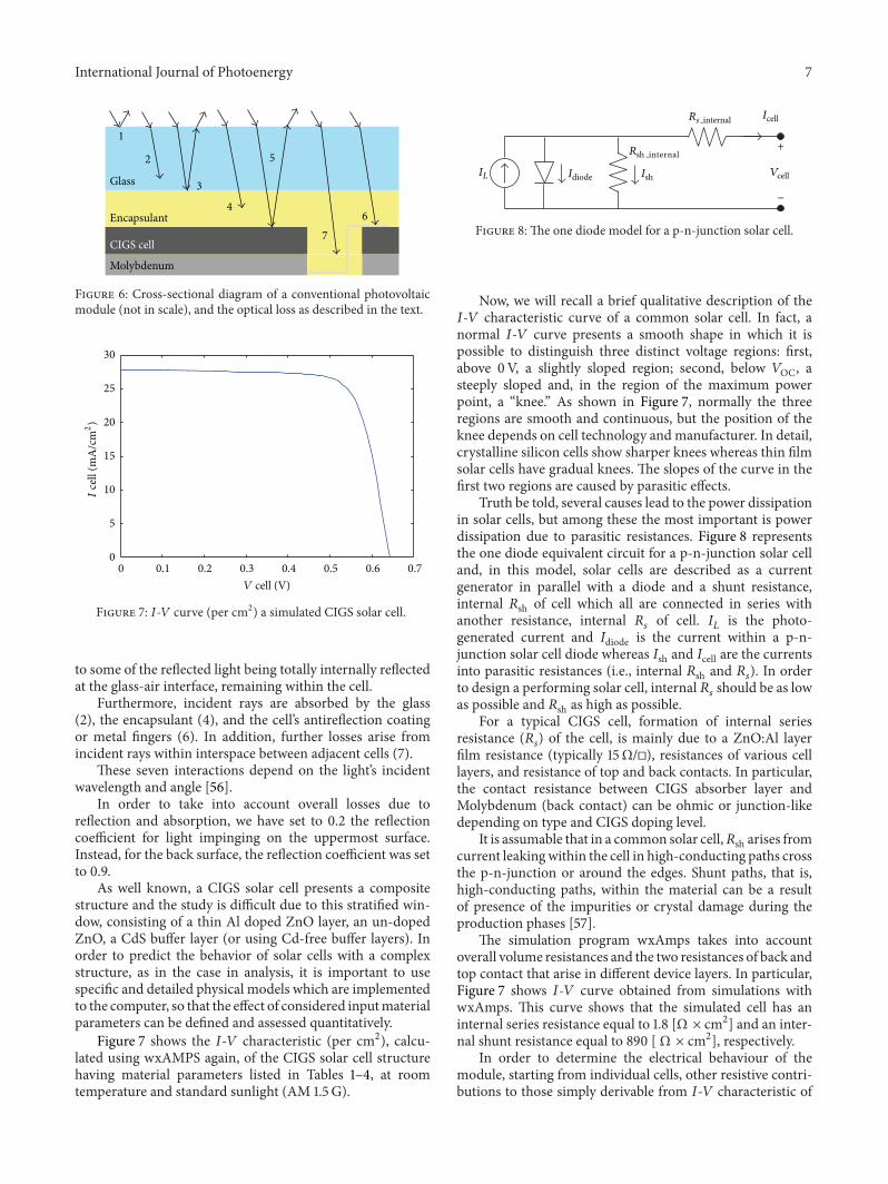