Research Article General Voltage Feedback Circuit Model in...
9
Research Article General Voltage Feedback Circuit Model in the Two-Dimensional Networked Resistive Sensor Array JianFeng Wu, 1 Lei Wang, 2 and JianQing Li 1 1 Jiangsu Key Lab of Remote Measurement and Control, School of Instrument Science and Engineering, Southeast University, Nanjing 210096, China 2 School of Automation, Nanjing Institute of Technology, Nanjing 211167, China Correspondence should be addressed to JianFeng Wu; [email protected] Received 14 January 2015; Accepted 14 June 2015 Academic Editor: Stefania Campopiano Copyright © 2015 JianFeng Wu et al. is is an open access article distributed under the Creative Commons Attribution License, which permits unrestricted use, distribution, and reproduction in any medium, provided the original work is properly cited. To analyze the feature of the two-dimensional networked resistive sensor array, we firstly proposed a general model of voltage feedback circuits (VFCs) such as the voltage feedback non-scanned-electrode circuit, the voltage feedback non-scanned-sampling- electrode circuit, and the voltage feedback non-scanned-sampling-electrode circuit. By analyzing the general model, we then gave a general mathematical expression of the effective equivalent resistor of the element being tested in VFCs. Finally, we evaluated the features of VFCs with simulation and test experiment. e results show that the expression is applicable to analyze the VFCs’ performance of parameters such as the multiplexers’ switch resistors, the nonscanned elements, and array size. 1. Introduction e networked resistive sensor array in row-column fashion played a key role in various sensing applications such as tactile sensing [1–8], temperature sensing [8, 9], and photoconduc- tive image sensing [10, 11], in which every sensitive element had two ends with one end connected to a row line and the other end connected to a column line. us, the interconnect line number of the × resistive sensor array was reduced to +. To have individual access of all elements in the two- dimensional (2D) networked resistive sensor array, many measurement methods such as the inserting diode method [3], the passive integrators method [5], the same potential method [8, 10–13], and the voltage feedback method (VFM) [1, 2, 9, 14–18] were proposed and their performances were evaluated. In these methods, VFM was proven to be an efficient technique. In the sensor array, parameters such as array size and nonscanned elements affected the measurement error of the element being tested (EBT) for the crosstalk caused by parasitic parallel paths. VFMs with op-amps and many multiplexers were proposed for virtually isolating the EBT from the 2D networked resistive sensor array; thus, the EBT could be tested precisely. Different VFMs [15], such as the voltage feedback non-scanned-electrode (VF-NSE) method, the voltage feedback non-scanned-sampling-electrode (VF- NSSE) method, and the voltage feedback non-scanned- driving-electrode (VF-NSDE) method, had different perfor- mances. But the multiplexer’s switch resistor induced extra errors on the EBT. Moreover, the operating mechanism of these parameters in different VFMs has not been understood completely. Performances of three hardware circuits in the 2D networked resistive sensor array were evaluated in [5]. In some literatures, performances of the parameters in the 2D networked resistive sensor array were evaluated with the circuit simulation soſtware such as CADENCE-SPCTRE and PSpice [12–15]. Liu et al. [15] compared the VF-NSE method, the VF-NSSE method, and the VF-NSDE method with PSpice. Although circuit simulation was useful for accurate prediction of the EBT’s measurement error, it consumed a large amount of manual work. us, circuit simulation was not convenient for fast complicated analyses of VFCs in the 2D networked resistive sensor array. With a general Hindawi Publishing Corporation Journal of Sensors Volume 2015, Article ID 913828, 8 pages http://dx.doi.org/10.1155/2015/913828
Transcript of Research Article General Voltage Feedback Circuit Model in...
Research ArticleGeneral Voltage Feedback Circuit Model in theTwo-Dimensional Networked Resistive Sensor Array
JianFeng Wu,1 Lei Wang,2 and JianQing Li1
1 Jiangsu Key Lab of Remote Measurement and Control, School of Instrument Science and Engineering, Southeast University,Nanjing 210096, China2School of Automation, Nanjing Institute of Technology, Nanjing 211167, China
Correspondence should be addressed to JianFeng Wu; [email protected]
Received 14 January 2015; Accepted 14 June 2015
Academic Editor: Stefania Campopiano
Copyright © 2015 JianFeng Wu et al. This is an open access article distributed under the Creative Commons Attribution License,which permits unrestricted use, distribution, and reproduction in any medium, provided the original work is properly cited.
To analyze the feature of the two-dimensional networked resistive sensor array, we firstly proposed a general model of voltagefeedback circuits (VFCs) such as the voltage feedback non-scanned-electrode circuit, the voltage feedback non-scanned-sampling-electrode circuit, and the voltage feedback non-scanned-sampling-electrode circuit. By analyzing the general model, we then gavea general mathematical expression of the effective equivalent resistor of the element being tested in VFCs. Finally, we evaluatedthe features of VFCs with simulation and test experiment. The results show that the expression is applicable to analyze the VFCs’performance of parameters such as the multiplexers’ switch resistors, the nonscanned elements, and array size.
1. Introduction
The networked resistive sensor array in row-column fashionplayed a key role in various sensing applications such as tactilesensing [1–8], temperature sensing [8, 9], and photoconduc-tive image sensing [10, 11], in which every sensitive elementhad two ends with one end connected to a row line and theother end connected to a column line.Thus, the interconnectline number of the𝑀×𝑁 resistive sensor array was reducedto𝑀+𝑁. To have individual access of all elements in the two-dimensional (2D) networked resistive sensor array, manymeasurement methods such as the inserting diode method[3], the passive integrators method [5], the same potentialmethod [8, 10–13], and the voltage feedback method (VFM)[1, 2, 9, 14–18] were proposed and their performances wereevaluated. In these methods, VFM was proven to be anefficient technique.
In the sensor array, parameters such as array size andnonscanned elements affected the measurement error ofthe element being tested (EBT) for the crosstalk causedby parasitic parallel paths. VFMs with op-amps and manymultiplexers were proposed for virtually isolating the EBT
from the 2D networked resistive sensor array; thus, the EBTcould be tested precisely. Different VFMs [15], such as thevoltage feedback non-scanned-electrode (VF-NSE) method,the voltage feedback non-scanned-sampling-electrode (VF-NSSE) method, and the voltage feedback non-scanned-driving-electrode (VF-NSDE) method, had different perfor-mances. But the multiplexer’s switch resistor induced extraerrors on the EBT. Moreover, the operating mechanism ofthese parameters in different VFMs has not been understoodcompletely.
Performances of three hardware circuits in the 2Dnetworked resistive sensor array were evaluated in [5]. Insome literatures, performances of the parameters in the 2Dnetworked resistive sensor array were evaluated with thecircuit simulation software such as CADENCE-SPCTRE andPSpice [12–15]. Liu et al. [15] compared the VF-NSE method,the VF-NSSE method, and the VF-NSDE method withPSpice. Although circuit simulation was useful for accurateprediction of the EBT’s measurement error, it consumeda large amount of manual work. Thus, circuit simulationwas not convenient for fast complicated analyses of VFCsin the 2D networked resistive sensor array. With a general
Hindawi Publishing CorporationJournal of SensorsVolume 2015, Article ID 913828, 8 pageshttp://dx.doi.org/10.1155/2015/913828
2 Journal of Sensors
Follower
Controller
(IV) NSE
(III) NSDE(II) NSSE
(I) BasicVI
R11
Rsr
Rsr
Rsg
Rsr
Rsc Rsc Rsc
R12 R1N
R21 R22 R2N
RM1 RM2 RMN
VF = Vsg
Vcy
Vrx
IM1
I21
I11−
+
0 0
00
00
Vsg
· · ·
· · ·
· · ·
· · ·· · ·· · ·· · · · · ·
· · ·
(a)
(III) NSDE
(II) NSSE
(IV) NSE
(I) Basic
R11
R22
R23
R2N RrdR13
R1N
Rsc
Rsc
Rsc
R12
RM2
RM3
RMNRsr
Rsr
RM1
R21Rcu
...
...
...
Node Vsg
Node R2
Node R1
Node RM
Node RVF Node CN
Node C3Node C1
Node CVF
Node C2
Node VI
(b)
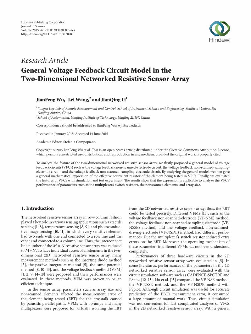
Figure 1: VFCs and their topological structures: (a) VFCs; (b) topological structures.
mathematical expression of the EBT’s effective equivalentresistor (𝑅EQ), fast evaluation of different parameters in dif-ferentVFCs could be realized by themathematical simulationsoftware. Saxena et al. [12, 13] analyzed the effect of array sizeon the EBT’s measurement error in the equipotential methodand proposed the approximate mathematical expression.Theresults of the measurement voltage errors in the three VFCssuch as VF-NSE circuit, VF-NSSE circuit, and VF-NSDEcircuit were given by circuit simulations [15, 16]. But, inVFCs,the voltage could not directly represent the EBT’s resistancevalue. Less theoretical analysis was implemented inVFCs andthemathematical expression of the𝑅EQ applicable to differentVFCs was still lacking.
For this purpose, we analyzed voltage feedback circuits(as shown in Figure 1(a)) in the 2D networked resistive sensorarray. In these circuits, the VF methods were utilized andthe sample resistors were connected with the power ground.This paper was organized as follows. Section 1 introducedthe existing measurement methods. Section 2 provided thegeneral model of voltage feedback circuits and its mathe-matical expression of the EBT’s effective equivalent resis-tance. Section 3 presented experiment results and discussion.Finally, Section 4 provided conclusions.
2. General Approximate Circuit Model of VFCs
In VFCs (Figure 1(a)), the feedback voltage (𝑉𝐹) was equal
to 𝑉𝑠𝑔. In the basic circuit, no 𝑉
𝐹was connected with
the nonscanned switches and no voltage drove the non-scanned electrodes. In VF-NSSE circuit, 𝑉
𝐹was connected
with the non-scanned-sampling switches and it drove thenon-scanned-sampling electrodes. In VF-NSDE circuit, 𝑉
𝐹
was connected with the non-scanned-driving switches andit drove the non-scanned-driving electrodes. In VF-NSEcircuit, 𝑉
𝐹was connected with all nonscanned switches and
it drove all nonscanned electrodes.In VFCs, we could use the 𝑅EQ between 𝑉
𝐼and 𝑉
𝑠𝑔to
represent the EBT’s measurement value. The general topo-logical structure of the 𝑅EQ was shown in Figure 1(b). Everysampling Node 𝑅
𝑖(the 𝑖th shared row line) was connected
with all𝑁 driving nodes (all shared column lines) with everyconnection of a column adjacent resistor (𝑅
𝑖1, . . . , 𝑅
𝑖𝑁). Every
driving Node 𝐶𝑗(the 𝑗th shared column line) was connected
with all𝑀 sampling nodes (all shared row lines) with everyconnection of a row adjacent resistor (𝑅
𝑗1, . . . , 𝑅
𝑗𝑀). 𝑅𝑖𝑗(𝑅11
in Figure 1) was the EBT, which connected Node 𝑅𝑖to Node
𝐶𝑗. 𝑅𝑐𝑢
connected Node 𝐶𝑗to Node 𝑉
𝐼. 𝑅𝑟𝑑
connected

Journal of Sensors 3
Rsc
Rb
Re
Rd
VI Vcy
Vrx
VF
Vrx VsgRxy Rrd
RsgRgRcRcu
Ra
Icu Ixy
IP
Isg
(III) NSDE (II) NSSE
(IV) NSE
(I) Basic
− +
Rf
Rsr
Radjc
Radjr
Rnadj
REQ
VGnd
Figure 2: General approximate circuit model of VFCs in the 2Dnetworked resistive sensor array.
Table 1: Parameters in the general circuit model of VFCs.
Basic VF-NSSE VF-NSDE VF-NSE𝑅𝑎
𝑅adj𝑟/(𝑀− 1)𝑅𝑏∞ 𝑅
𝑠𝑟/(𝑀− 1) ∞ 𝑅
𝑠𝑟/(𝑀− 1)
𝑅𝑐
𝑅𝑥𝑦
𝑅𝑑∞ ∞ 𝑅
𝑠𝑐/(𝑁 − 1) 𝑅
𝑠𝑐/(𝑁 − 1)
𝑅𝑒
𝑅nadj/(𝑀− 1)/(𝑁 − 1)𝑅𝑓
𝑅adj𝑐/(𝑁 − 1)𝑅𝑔
𝑅𝑟𝑑
Node 𝑅𝑖to Node 𝑉
𝑠𝑔. Node 𝑅
𝑉𝐹was connected with the
non-scanned-sampling nodes with 𝑅𝑠𝑟and the non-scanned-
driving nodes with 𝑅𝑠𝑐.
The structure represented the basic circuit when noconnection existed between 𝑉
𝐹and the nonscanned elec-
trodes; the structure represented VF-NSSE circuit when theconnections only existed between 𝑉
𝐹and the non-scanned-
sampling electrodes; the structure represented VF-NSDEcircuit when the connections only existed between𝑉
𝐹and the
non-scanned-driving electrodes; the structure representedVF-NSE circuitwhen the connections existed between𝑉
𝐹and
the nonscanned electrodes.If each group of elements such as all adjacent non-
scanned-sampling elements (𝑅adj𝑟s), all adjacent non-scanned-driving elements (𝑅adj𝑐s), all nonadjacent elements(𝑅nadjs), all 𝑅𝑠𝑟s, and all 𝑅
𝑠𝑐s had similar resistance values,
voltages on NSSE and voltages on NSDE would be similar.So, the 𝑅EQ topological structure could be simplified to ageneral approximate circuit model as shown in Figure 2.When the parameter of each element in VFCs varied a little,the differences of voltages in different NSSE circuit and thedifferences of voltages in different NSDE circuit were tiny.Thus, the circuit model could also be used to analyze VFCswith one element or one group of elements that varied a little.
In Figure 2, 𝑅𝑎represented all 𝑅adj𝑐s; 𝑅𝑏 represented all
𝑅𝑠𝑐s; 𝑅𝑐represented the EBT; 𝑅
𝑑represented all 𝑅
𝑠𝑟s; 𝑅𝑒rep-
resented all 𝑅nadjs; 𝑅𝑓 represented all 𝑅adj𝑟s; 𝑅𝑔 represented𝑅𝑟𝑑. Table 1 defined parameters in the general approximate
circuit model of VFCs.
VI
VcyVrx Vsg
RsgRgRc
Re1Rd1
Rd2
Rb1
Rb2
RbRa
Rcu
Icu
Ixy
Isg
REQ
VGnd = 0
Figure 3: Star-delta conversion result of the part including 𝑅𝑑, 𝑅𝑒,
and 𝑅𝑓.
In the three VFCs, the currents such as 𝐼𝑥𝑦, 𝐼𝑠𝑔, and 𝐼
𝑐𝑢
were different for the current on parasitic parallel resistors(𝐼𝑝). So, the measurement accuracies of the EBT in the
three VFCs were different. In this paper, we hoped topropose a general mathematical expression of the 𝑅EQ whichcould clarify the relation between parameters and the EBT’smeasurement accuracy in VFCs.
Taking VF-NSE circuit, for example, we solved its 𝑅EQ. Ifthe op-amp was an ideal amplifier, then 𝑉
𝐹was equal to 𝑉
𝑠𝑔.
With star-delta conversion, the part including 𝑅𝑑, 𝑅𝑒, and 𝑅
𝑓
in Figure 2 could be converted to the part including 𝑅𝑑1, 𝑅𝑒1,
and 𝑅𝑏1as shown in Figure 3.
Thus, 𝑅𝑒1, 𝑅𝑑1, and 𝑅
𝑏1could be expressed as the follow-
ing equation, as shown in Figure 3:
𝑅𝑒1 = 𝑅𝑒 +𝑅𝑓 +
𝑅𝑒𝑅𝑓
𝑅𝑑
,
𝑅𝑑1 = 𝑅𝑑 +𝑅𝑓 +
𝑅𝑓𝑅𝑑
𝑅𝑒
,
𝑅𝑏1 = 𝑅𝑑 +𝑅𝑒 +
𝑅𝑒𝑅𝑑
𝑅𝑓
.
(1)
Thus, 𝑅𝑏2
and 𝑅𝑑2
in Figure 3 could be expressed asfollows:
𝑅𝑏2 =𝑅𝑏𝑅𝑏1
𝑅𝑏+ 𝑅𝑏1,
𝑅𝑑2 =𝑅𝑔𝑅𝑑1
𝑅𝑔+ 𝑅𝑑1.
(2)
With star-delta conversion, the part including 𝑅𝑎, 𝑅𝑐,
and 𝑅𝑒1in Figure 3 could be converted to the part including
𝑅1, 𝑅2, and 𝑅
3as shown in Figure 4(a); the part including
𝑅𝑒1, 𝑅𝑏2, and 𝑅
𝑑2in Figure 3 could be converted to the part
including 𝑅4, 𝑅5, and 𝑅
6as shown in Figure 4(b).

4 Journal of Sensors
VI
VcyVsg
Rcu R1
R2
Rsg
Rb2
Rd2R3
VGnd = 0
(a)
VI
VcyVsg
Rcu R6
Rc R5
Ra R4
Rsg
VGnd = 0
(b)
Figure 4: Star-delta conversion results. (a) The part including 𝑅𝑎, 𝑅𝑐, and 𝑅
𝑒1. (b) The part including 𝑅
𝑒1, 𝑅𝑏2, and 𝑅
𝑑2.
Thus, 𝑅1, 𝑅2, and 𝑅
3in Figure 4(a) could be expressed as
the following equation:
𝑅1 =𝑅𝑎𝑅𝑐
𝑅𝑎+ 𝑅𝑐+ 𝑅𝑒1,
𝑅2 =𝑅𝑎𝑅𝑒1
𝑅𝑎+ 𝑅𝑐+ 𝑅𝑒1,
𝑅3 =𝑅𝑐𝑅𝑒1
𝑅𝑎+ 𝑅𝑐+ 𝑅𝑒1.
(3)
Thus, 𝑅4, 𝑅5, and 𝑅
6in Figure 4(b) could be expressed as
the following equation:
𝑅4 =𝑅𝑏2𝑅𝑒1
𝑅𝑏2 + 𝑅𝑑2 + 𝑅𝑒1
,
𝑅5 =𝑅𝑑2𝑅𝑒1
𝑅𝑏2 + 𝑅𝑑2 + 𝑅𝑒1
,
𝑅6 =𝑅𝑏2𝑅𝑑2
𝑅𝑏2 + 𝑅𝑑2 + 𝑅𝑒1
.
(4)
In the case that 𝑉𝐼was a constant in VFCs, from the
port of the sample resistor (𝑅𝑠𝑔), the general mathematical
expression of the 𝑅EQ in VFCs could be expressed as follows:
𝑅EQ =𝐼𝑐𝑢𝑅𝑐𝑢+ 𝐼𝑥𝑦𝑅𝑐+ 𝐼𝑠𝑔𝑅𝑟𝑑
𝐼𝑠𝑔
= (𝑅3 + 𝑅𝑑2𝑅2 + 𝑅𝑏2
+ 1)
⋅ (1+𝑅𝑟𝑑
𝑅𝑑1)(𝑅𝑐𝑢+𝑅4 + 𝑅𝑎
𝑅4 + 𝑅5 + 𝑅𝑎 + 𝑅𝑥𝑦𝑅𝑥𝑦)+𝑅𝑟𝑑.
(5)
Equation (5) was also suitable for the basic circuit, VF-NSSE circuit, and VF-NSDE circuit. Thus, we could use (5)to analyze the performance of parameters in VFCs.
3. Experiments and Discussion
3.1. Simulation Experiment. For verifying the applicability ofthe general mathematical expression of the 𝑅EQ in VFCs, wesimulated (5) in MATLAB and VFCs in NI Multisim 12 forcomparison. InNIMultisim, the voltage on𝑅
𝑠𝑔wasmeasured
and then the 𝑅𝑥𝑦
could be obtained.
3.1.1. The 𝑅𝑥𝑦
Range Effect Simulation. The EBT’s resistancevalue affected its measurement errors. In evaluating the effectof𝑅𝑥𝑦range, the other parameters were set to constant values.
3
2
1
0
−1
−2
−3
−4
−5
−6
−70.1 1 10 100 1000
MATLAN VF-NSENI VF-NSEMATLAB VF-NSSE
MATLAB VF-NSDENI VF-NSSENI VF-NSDE
0.2
0.1
0.0
−0.15 10 15 20 25 30
Rxy with Rswitch = 1Ω (kΩ)
Rxy
erro
r with
Rot
her=10
kΩan
dM
=N
=8
(%)
Figure 5: Simulation results of the 𝑅𝑥𝑦
range effect in VFCs.
We fixed𝑀 and𝑁 at 8, 𝑅switch at 1Ω, and the resistance valueof 𝑅𝑠𝑔and all nonscanned elements in the 2D resistive sensor
array at 10 kΩ. The three VFCs were simulated with 𝑅𝑥𝑦
varying in 0.10 kΩ–1000 kΩ. Figure 5 showed the simulationresults.
When 𝑅𝑥𝑦
varied in 0.10 kΩ–1000 kΩ, the 𝑅𝑥𝑦
errors ofMATLAB in every VFC were a little bigger than its 𝑅
𝑥𝑦
errors of the NI simulation with similar changing pattern;the 𝑅𝑥𝑦
errors in VF-NSE circuit were the biggest and thosein VF-NSDE circuit were the smallest. In Figure 8, when 𝑅
𝑥𝑦
increased in the three VFCs, the 𝑅𝑥𝑦
errors decreased whilethe difference between the simulation results of MATLABand those of NI increased.
3.1.2. The Switch Resistor (𝑅𝑠𝑤𝑖𝑡𝑐ℎ
) Effect Simulation. In eval-uating the effect of 𝑅switch, the other parameters were set toconstant values. In simulations, we fixed𝑀 and 𝑁 at 8 andfixed the resistance value of 𝑅
𝑠𝑔and all elements in the sensor
array at 10 kΩ. The three VFCs were simulated with 𝑅switchthat varied in 0.10Ω–100Ω, such as 𝑅
𝑠𝑐with 𝑅
𝑠𝑟= 1Ω, 𝑅
𝑠𝑟
with𝑅𝑠𝑐= 1Ω, and𝑅
𝑠𝑟= 𝑅𝑠𝑐. Figure 6 showed the simulation
results.With similar values of the 𝑅
𝑥𝑦errors, simulation curves
could be divided into four groups: the VF-NSE errors with
Journal of Sensors 5
Rswitch (Ω)0.1 1 10 100
16
14
12
10
8
6
4
2
0
Rxy
erro
r with
Rxy=10
kΩ
Rswitch change with Rsc = Rsr in MATLAB NSERswitch change with Rsc = Rsr in NI NSERswitch change with Rsc = Rsr in MATLAB NSSERswitch change with Rsc = Rsr in MATLAB NSDERswitch change with Rsc = Rsr in NI NSSERswitch change with Rsc = Rsr in NI NSDE Rsc = Rsr
Rsr change in NI NSE with Rsc = 1Ω
Rsc change in NI NSE with Rsr = 1Ω
Rsc change in NI NSSE with Rsr = 1Ω
Rsr change in NI NSDE with Rsc = 1Ω
Rsr change in MATLAB NSE with Rsc = 1Ω
Rsc change in MATLAB NSSE with Rsr = 1Ω
Rsr change in MATLAB NSDE with Rsc = 1Ω
Rsc change in MATLAB NSE with Rsr = 1Ω
Rsc change in MATLAB NSDE with Rsr = 1Ω
Rsr change in MATLAB NSSE with Rsc = 1Ω
Rsr change in NI NSSE with Rsc = 1Ω
Rsc change in NI NSDE with Rsr = 1Ω
andM
=N
=8
in V
FC (%
)
Figure 6: Simulation results of the 𝑅switch effect in VFCs.
𝑅𝑠𝑟= 𝑅𝑠𝑐were similar in MATLAB and in NI, which were
the biggest; with 𝑅𝑠𝑟= 𝑅𝑠𝑐, the VF-NSSE errors and the VF-
NSDE errors were similar inMATLAB and inNI, which werethe second biggest; the VF-NSDE errors with 𝑅
𝑠𝑟= 1Ω and
the VF-NSSE errors with 𝑅𝑠𝑐= 1Ω were similar in MATLAB
and in NI, which were the smallest; other errors were similar,which were the third biggest.
From Figure 6, we also found that, with 𝑅switch varying in0.10Ω–100Ω, the 𝑅
𝑥𝑦errors of MATLAB in every VFC were
similar to its𝑅𝑥𝑦errors of theNI simulation; with the increase
of 𝑅switch in this simulation, the 𝑅𝑥𝑦
errors of the three VFCshad positive coefficients.
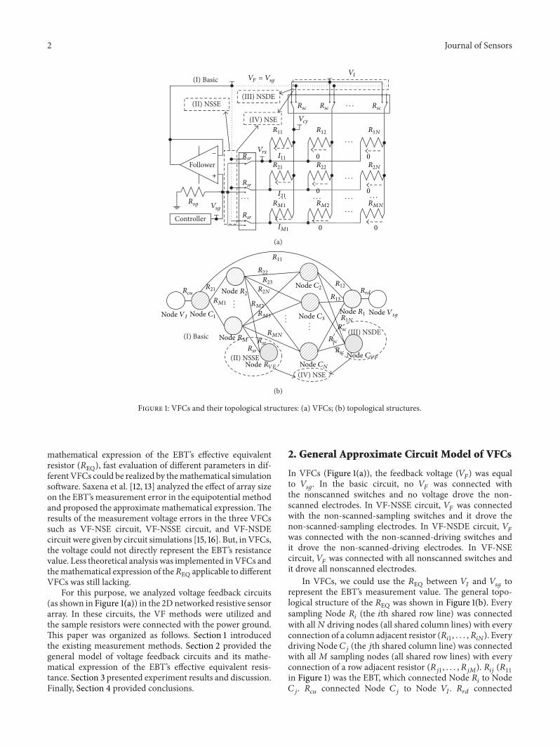
3.1.3. The Array Size Effect Simulation. Parameters of arraysize such as the number of sampling lines (𝑀) and thenumber of driving lines (𝑁) were proved to have similarinfluences on the performance of the 2D networked resistivesensor arrays [15]. In simulations, we fixed some parametersincluding the resistance value of the sample resistor and allelements in resistive sensor array at 10 kΩ,𝑀 or 𝑁 at 8, and𝑅switch at 1Ω;𝑁 or𝑀was one of 8, 14, 26, 50, 98, 194, and 386.Figure 7 showed the simulation results.
M change of NSE with N = 8 in MATLABN change of NSE with M = 8 in MATLABM change of NSSE with N = 8 in MATLABN change of NSDE with M = 8 in MATLABM change of NSE with N = 8 in NIM change of NSSE with N = 8 in NIN change of NSE with M = 8 in NIN change of NSDE with M = 8 in NIM change of NSDE with N = 8 in MATLABN change of NSSE with M = 8 in MATLABM change of NSDE with N = 8 in NIN change of NSSE with M = 8 in NI
Array size8 16 32 64 128 256 512
Rxy
erro
r with
Rxy=10
kΩan
dR
switc
h=1Ω
in V
FC (%
)
4.0
3.5
3.0
2.5
2.0
1.5
1.0
0.5
0.0
Figure 7: Simulation results of the array size effect in VFCs.
With the change of array size, the 𝑅𝑥𝑦
errors of MATLABin every VFC were similar to its 𝑅
𝑥𝑦errors of the NI
simulation. With the increase of𝑀 or 𝑁 in VF-NSE circuit,the 𝑅
𝑥𝑦errors had significant positive coefficients. In VF-
NSSE circuit, the 𝑅𝑥𝑦
errors also had significant positivecoefficients with the increase of 𝑀, whereas the 𝑅
𝑥𝑦errors
had small negative coefficients with the increase of𝑁. In VF-NSDE circuit, the 𝑅
𝑥𝑦errors had tiny negative coefficients
with the increase of𝑀, whereas the𝑅𝑥𝑦errors had significant
positive coefficients with the increase of𝑁. With the increaseof𝑀 or𝑁, the 𝑅
𝑥𝑦errors in VF-NSE circuit were bigger than
those of VF-NSSE circuit and VF-NSDE circuit.
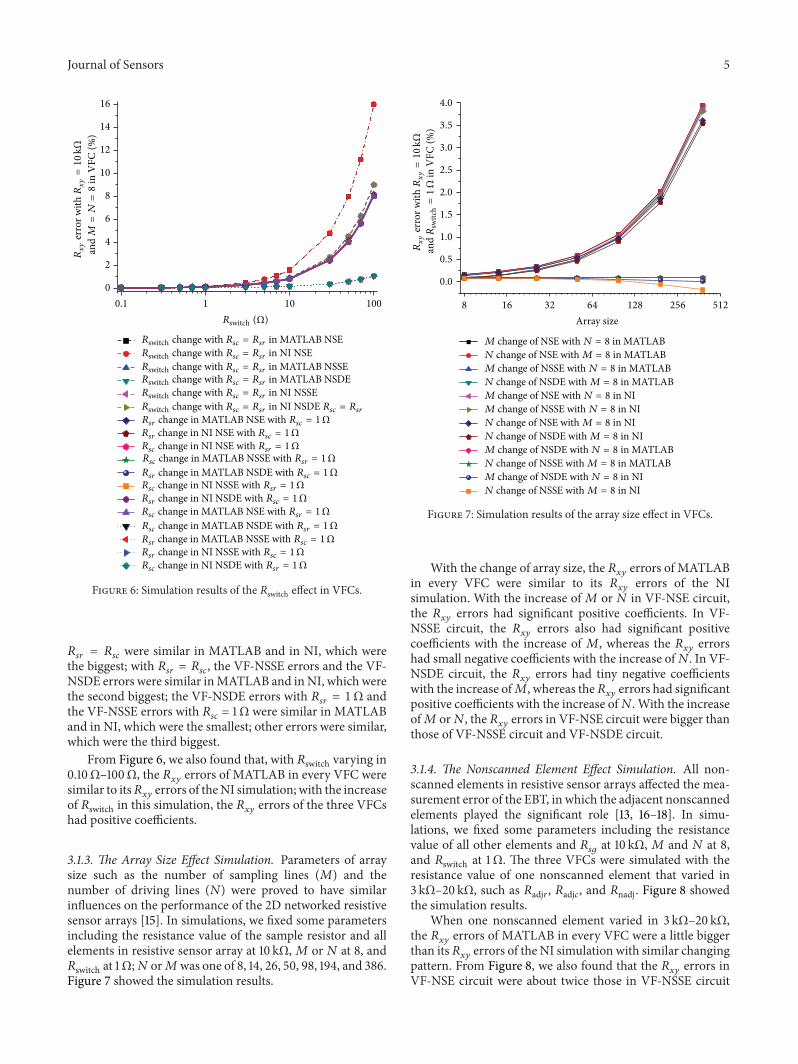
3.1.4. The Nonscanned Element Effect Simulation. All non-scanned elements in resistive sensor arrays affected the mea-surement error of the EBT, in which the adjacent nonscannedelements played the significant role [13, 16–18]. In simu-lations, we fixed some parameters including the resistancevalue of all other elements and 𝑅
𝑠𝑔at 10 kΩ,𝑀 and 𝑁 at 8,
and 𝑅switch at 1Ω. The three VFCs were simulated with theresistance value of one nonscanned element that varied in3 kΩ–20 kΩ, such as 𝑅adj𝑟, 𝑅adj𝑐, and 𝑅nadj. Figure 8 showedthe simulation results.
When one nonscanned element varied in 3 kΩ–20 kΩ,the 𝑅𝑥𝑦
errors of MATLAB in every VFC were a little biggerthan its𝑅
𝑥𝑦errors of the NI simulation with similar changing
pattern. From Figure 8, we also found that the 𝑅𝑥𝑦
errors inVF-NSE circuit were about twice those in VF-NSSE circuit
6 Journal of Sensors
0.18
0.16
0.14
0.12
0.10
0.08
Rxy
erro
r with
Rxy=10
kΩ
4 6 8 10 12 14 16 18 20
One nonscanned element (kΩ)
Radjc in NSE MATLABRadjr in NSE MATLABRadjr in NSE NIRadjc in NSE NIRnadj in NSE MATLABRnadj in NSE NIRadjc in NSDE MATLABRadjr in NSSE MATLABRnadj in NSSE MATLAB
Rnadj in NSDE MATLABRadjc in NSSE MATLABRadjr in NSDE MATLABRadjr in NSSE NIRnadj in NSSE NIRadjc in NSDE NIRadjr in NSDE NIRadjc in NSSE NIRnadj in NSDE NI
andM
=N
=8
in V
FC (%
)
Figure 8: Simulation results of the one nonscanned element effectin VFCs.
andVF-NSDE circuit.With one nonadjacent element varyingfrom 3 kΩ to 20 kΩ, the changes of the 𝑅
𝑥𝑦errors in the three
VFCs were insignificant. With one 𝑅adj𝑟 or one 𝑅adj𝑐 varyingfrom 3 kΩ to 20 kΩ, the changes of the 𝑅
𝑥𝑦errors in VF-NSE
circuit were significant, while those in VF-NSSE circuit andVF-NSDE circuit were insignificant; the 𝑅
𝑥𝑦errors in VF-
NSE circuit were the biggest and the 𝑅𝑥𝑦
errors in VF-NSDEcircuit were the smallest.
3.2. The Test Experiment. An experimental device with an 8× 16 element array was designed for verifying the features ofthree VFCs. In the device, OPA2340 (from the datasheet, theoffset voltage, the bias current, the gain-bandwidth, and thegain are equal to 150𝜇V, 0.2 pA, 5.5MHz, and 100 dB, resp.)was used as the op-amp, and ADG884 (from the datasheet,the on-resistance, the on-resistance match between channels,and the on-resistance flatness are equal to 0.41Ω, 0.05Ω, and0.15Ω, resp.) was used as the multiplex switch.
In experiments, the EBTwas replaced by a precision resis-tance box with its smallest step resistance value at 0.1Ω, theadjacent elements were also replaced by precision resistanceboxes, and the nonadjacent elements were precision resistorswith each resistance value at 4.7 kΩ.
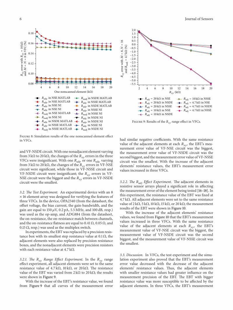
3.2.1. The 𝑅𝑥𝑦
Range Effect Experiment. In the 𝑅𝑥𝑦
rangeeffect experiment, all adjacent elements were set to the sameresistance value of 4.7 kΩ, 10 kΩ, or 20 kΩ. The resistancevalue of the EBT was varied from 2 kΩ to 20 kΩ; the resultswere shown in Figure 9.
With the increase of the EBT’s resistance value, we foundfrom Figure 9 that all curves of the measurement error
2 4 6 8 10 12 14 16 18 20
0.00.51.01.52.0
Radj = 20kΩ in NSERadj = 20kΩ in NSDERadj = 20kΩ in NSSERadj = 10kΩ in NSERadj = 10kΩ in NSDE
Radj = 10kΩ in NSSERadj = 4.7 kΩ in NSERadj = 4.7kΩ in NSDERadj = 4.7kΩ in NSSE
Rxy (kΩ)
−5.5−5.0−4.5−4.0−3.5−3.0−2.5−2.0−1.5−1.0−0.5
Rxy
erro
r with
M=8,N
=16
andR
nadj=4.7
kΩ(%
)Figure 9: Results of the 𝑅
𝑥𝑦range effect in VFCs.
had similar negative coefficients. With the same resistancevalue of the adjacent elements at each 𝑅
𝑥𝑦, the EBT’s mea-
surement error value of VF-NSE circuit was the biggest,the measurement error value of VF-NSDE circuit was thesecond biggest, and themeasurement error value of VF-NSSEcircuit was the smallest. With the increase of the adjacentelements’ resistance values, the EBT’s measurement errorvalues increased in three VFCs.
3.2.2. The 𝑅𝑎𝑑𝑗
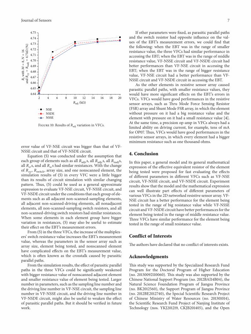
Effect Experiment. The adjacent elements inresistive sensor arrays played a significant role in affectingthemeasurement error of the element being tested [16–18]. Inthis experiment, the resistance value of the EBT was fixed at4.7 kΩ. All adjacent elements were set to the same resistancevalue of 2 kΩ, 5 kΩ, 10 kΩ, 15 kΩ, or 20 kΩ; the measurementresults of the EBT were shown in Figure 10.
With the increase of the adjacent elements’ resistancevalues, we found from Figure 10 that the EBT’s measurementvalues increased in three VFCs. With the same resistancevalue of the adjacent elements at each 𝑅
𝑥𝑦, the EBT’s
measurement value of VF-NSE circuit was the biggest, themeasurement value of VF-NSDE circuit was the secondbiggest, and the measurement value of VF-NSSE circuit wasthe smallest.
3.3. Discussion. In VFCs, the test experiment and the simu-lation experiment also proved that the EBT’s measurementerror value decreased with the decrease of the adjacentelements’ resistance values. Thus, the adjacent elementswith smaller resistance values had greater influence on themeasurement precision of the EBT. The EBT with biggerresistance value was more susceptible to be affected by theadjacent elements. In three VFCs, the EBT’s measurement
Journal of Sensors 7
2 4 6 8 10 12 14 16 18 204.644.654.664.674.684.694.704.714.724.734.744.75
NSENSDENSSE
Radj (kΩ)
Rt
with
M=8,N
=16
andRxy=R
nadj=4.7
kΩ(%
)
Figure 10: Results of 𝑅adj variation in VFCs.
error value of VF-NSE circuit was bigger than that of VF-NSSE circuit and that of VF-NSDE circuit.
Equation (5) was conducted under the assumption thateach group of elements such as all 𝑅adj𝑟s, all 𝑅adj𝑐s, all 𝑅nadjs,all 𝑅𝑠𝑟s, and all 𝑅
𝑠𝑐s had similar resistances. With the change
of 𝑅𝑥𝑦, 𝑅switch, array size, and one nonscanned element, the
simulation results of (5) in every VFC were a little biggerthan its results of circuit simulation with similar changingpattern. Thus, (5) could be used as a general approximateexpression to evaluate VF-NSE circuit, VF-NSSE circuit, andVF-NSDE circuit under the conditions that each group of ele-ments such as all adjacent non-scanned-sampling elements,all adjacent non-scanned-driving elements, all nonadjacentelements, all non-scanned-sampling switch resistors, and allnon-scanned-driving switch resistors had similar resistances.When some elements in each element group have biggervariation in resistances, (5) may also be useful to estimatetheir effect on the EBT’s measurement errors.
From (5) in the three VFCs, the increase of themultiplex-ers’ switch resistance value increases the EBT’s measurementvalue, whereas the parameters in the sensor array such asarray size, element being tested, and nonscanned elementhave complicated effects on the EBT’s measurement value,which is often known as the crosstalk caused by parasiticparallel paths.
From the simulation results, the effect of parasitic parallelpaths in the three VFCs could be significantly weakenedwith bigger resistance value of nonscanned adjacent elementand smaller resistance value of element being tested. Largernumber in parameters, such as the sampling line number andthe driving line number in VF-NSE circuit, the sampling linenumber in VF-NSSE circuit, and the driving line number inVF-NSDE circuit, might also be useful to weaken the effectof parasitic parallel paths. But it should be verified in futurework.
If other parameters were fixed, as parasitic parallel pathsand the switch resistor had opposite influence on the val-ues of the EBT’s measurement errors, we could find thatthe following: when the EBT was in the range of smallerresistance value, the three VFCs had similar performance inaccessing the EBT; when the EBT was in the range of middleresistance value, VF-NSSE circuit and VF-NSDE circuit hadbetter performances than VF-NSE circuit in accessing theEBT; when the EBT was in the range of bigger resistancevalue, VF-NSE circuit had a better performance than VF-NSSE circuit and VF-NSDE circuit in accessing the EBT.
As the other elements in resistive sensor array causedparasitic parallel paths, with smaller resistance values, theywould have more significant effects on the EBT’s errors inVFCs. VFCs would have good performances in the resistivesensor arrays, such as Thru Mode Force Sensing Resistor(FSR) array and Shunt Mode FSR array, in which the elementwithout pressure on it had a big resistance value and theelement with pressure on it had a small resistance value [4].At the same time, a precision op-amp in VFCs always had alimited ability on driving current, for example, tens of mAfor OP07. Thus, VFCs would have good performances in theresistive sensor arrays, in which every element had a biggerminimum resistance such as one thousand ohms.
4. Conclusion
In this paper, a general model and its general mathematicalexpression of the effective equivalent resistor of the elementbeing tested were proposed for fast evaluating the effectsof different parameters in different VFCs such as VF-NSEcircuit, VF-NSSE circuit, and VF-NSDE circuit. Experimentresults show that the model and the mathematical expressioncan well illustrate part effects of different parameters ofvarious VFCs in the 2D networked resistive sensor array. VF-NSE circuit has a better performance for the element beingtested in the range of big resistance value while VF-NSSEcircuit andVF-NSDE circuit have better performances for theelement being tested in the range of middle resistance value.Three VFCs have similar performance for the element beingtested in the range of small resistance value.
Conflict of Interests
The authors have declared that no conflict of interests exists.
Acknowledgments
This study was supported by the Specialized Research FundProgram for the Doctoral Program of Higher Education(no. 20130092110060). This study was also supported by theChinese National Support Program (no. 2012BAI14B04), theNatural Science Foundation Program of Jiangsu Province(no. BK2012560), the Support Program of Jiangsu Province(no. 2012BE2012740), the Special Scientific Research Projectof Chinese Ministry of Water Resources (no. 201301014),the Scientific Research Fund Project of Nanjing Institute ofTechnology (nos. YKJ201219, CKJB201405), and the Open
8 Journal of Sensors
Fund of the Key Laboratory of Remote Measurement andControl Technology in Jiangsu Province (nos. YCCK201401,YCCK201006).
References
[1] B. Tise, “A compact high resolution piezoresistive digital tactilesensor,” in Proceedings of the IEEE International Conference onRobotics and Automation, pp. 760–764, IEEE, New York, NY,USA, May 1988.
[2] T. H. Speeter, “A tactile sensing system for robotic manipula-tion,” The International Journal of Robotics Research, vol. 9, no.6, pp. 25–36, 1990.
[3] D. Prutchi and M. Arcan, “Dynamic contact stress analysisusing a compliant sensor array,”Measurement, vol. 11, no. 3, pp.197–210, 1993.
[4] K. F. de Jesus, M. H. Cheng, L. Jiang, and E. G. Bakhoum, “Res-olution enhancement method used for force sensing resistorarray,” Journal of Sensors, vol. 2015, Article ID 647427, 12 pages,2015.
[5] F. Vidal-Verdu, O. Oballe-Peinado, J. A. Sanchez-Duran, J.Castellanos-Ramos, and R. Navas-Gonzalez, “Three realiza-tions and comparison of hardware for piezoresistive tactilesensors,” Sensors, vol. 11, no. 3, pp. 3249–3266, 2011.
[6] C.-F. Hu, H.-Y. Huang, C.-C. Wen, L.-Y. Lin, and W. Fang,“Implementation of a flexible silicon-based tactile sensor array,”in Proceedings of the 9th IEEE Sensors Conference (SENSORS’10), pp. 1736–1739, IEEE, Kona, Hawaii, USA, November 2010.
[7] X. Zhang, Y. Zhao, and X. Zhang, “Design and fabrication of athin and soft tactile force sensor array based on conductiverubber,” Sensor Review, vol. 32, no. 4, pp. 273–279, 2012.
[8] Y.-J. Yang, M.-Y. Cheng, S.-C. Shih et al., “A 32×32 temperatureand tactile sensing array using PI-copper films,” The Interna-tional Journal of Advanced Manufacturing Technology, vol. 46,no. 9–12, pp. 945–956, 2010.
[9] J. F. Wu, L. Wang, J. Q. Li, and Z. Z. Yu, “A small size deviceusing temperature sensor array,” Chinese Journal of Sensors andActuators, vol. 24, no. 11, pp. 1649–1652, 2011 (Chinese).
[10] R. S. Saxena, R. K. Bhan, and A. Aggrawal, “A new discretecircuit for readout of resistive sensor arrays,” Sensors andActuators A: Physical, vol. 149, no. 1, pp. 93–99, 2009.
[11] D. Stratos, G.Maria, F. Eleftherios, and L. George, “Comparisonof three resistor network division circuits for the readout of 4×4pixel SiPM arrays,” Nuclear Instruments and Methods in PhysicsResearch, Section A: Accelerators, Spectrometers, Detectors andAssociated Equipment, vol. 702, pp. 121–125, 2013.
[12] R. S. Saxena, N. K. Saini, and R. K. Bhan, “Analysis of crosstalkin networked arrays of resistive sensors,” IEEE Sensors Journal,vol. 11, no. 4, pp. 920–924, 2011.
[13] R. S. Saxena, R. K. Bhan, N. K. Saini, and R.Muralidharan, “Vir-tual ground technique for crosstalk suppression in networkedresistive sensors,” IEEE Sensors Journal, vol. 11, no. 2, pp. 432–433, 2011.
[14] T. D’Alessio, “Measurement errors in the scanning of piezoresis-tive sensors arrays,” Sensors and Actuators A: Physical, vol. 72,no. 1, pp. 71–76, 1999.
[15] H. Liu, Y.-F. Zhang, Y.-W. Liu, and M.-H. Jin, “Measurementerrors in the scanning of resistive sensor arrays,” Sensors andActuators A: Physical, vol. 163, no. 1, pp. 198–204, 2010.
[16] J. F. Wu, L. Wang, and J. Q. Li, “VF-NSE method measurementerror analysis of networked resistive sensor array,” Sensors andActuators A: Physical, vol. 211, no. 5, pp. 45–50, 2014.
[17] J. F. Wu, L. Wang, and J. Q. Li, “Design and crosstalk erroranalysis of the circuit for the 2-D networked resistive sensorarray,” IEEE Sensors Journal, vol. 15, no. 2, pp. 1020–1026, 2015.
[18] J. F. Wu, L. Wang, J. Q. Li, and A. G. Song, “A novel crosstalksuppression method of the 2-D networked resistive sensorarray,” Sensors, vol. 14, no. 7, pp. 12816–12827, 2014.

International Journal of
AerospaceEngineeringHindawi Publishing Corporationhttp://www.hindawi.com Volume 2014
RoboticsJournal of
Hindawi Publishing Corporationhttp://www.hindawi.com Volume 2014
Hindawi Publishing Corporationhttp://www.hindawi.com Volume 2014
Active and Passive Electronic Components
Control Scienceand Engineering
Journal of
Hindawi Publishing Corporationhttp://www.hindawi.com Volume 2014
International Journal of
RotatingMachinery
Hindawi Publishing Corporationhttp://www.hindawi.com Volume 2014
Hindawi Publishing Corporation http://www.hindawi.com
Journal ofEngineeringVolume 2014
Submit your manuscripts athttp://www.hindawi.com
VLSI Design
Hindawi Publishing Corporationhttp://www.hindawi.com Volume 2014
Hindawi Publishing Corporationhttp://www.hindawi.com Volume 2014
Shock and Vibration
Hindawi Publishing Corporationhttp://www.hindawi.com Volume 2014
Civil EngineeringAdvances in
Acoustics and VibrationAdvances in
Hindawi Publishing Corporationhttp://www.hindawi.com Volume 2014
Hindawi Publishing Corporationhttp://www.hindawi.com Volume 2014
Electrical and Computer Engineering
Journal of
Advances inOptoElectronics
Hindawi Publishing Corporation http://www.hindawi.com
Volume 2014
The Scientific World JournalHindawi Publishing Corporation http://www.hindawi.com Volume 2014
SensorsJournal of
Hindawi Publishing Corporationhttp://www.hindawi.com Volume 2014
Modelling & Simulation in EngineeringHindawi Publishing Corporation http://www.hindawi.com Volume 2014
Hindawi Publishing Corporationhttp://www.hindawi.com Volume 2014
Chemical EngineeringInternational Journal of Antennas and
Propagation
International Journal of
Hindawi Publishing Corporationhttp://www.hindawi.com Volume 2014
Hindawi Publishing Corporationhttp://www.hindawi.com Volume 2014
Navigation and Observation
International Journal of
Hindawi Publishing Corporationhttp://www.hindawi.com Volume 2014
DistributedSensor Networks
International Journal of