Research and Development of Palladium/Metal Oxide Based ...
23
SUNY College of Environmental Science and Forestry SUNY College of Environmental Science and Forestry Digital Commons @ ESF Digital Commons @ ESF Honors Theses 5-2014 Research and Development of Palladium/Metal Oxide Based Research and Development of Palladium/Metal Oxide Based Nanostructures as High-Performance Hydrogen Gas Sensors Nanostructures as High-Performance Hydrogen Gas Sensors Jonathan Rice Follow this and additional works at: https://digitalcommons.esf.edu/honors Part of the Engineering Commons, and the Oil, Gas, and Energy Commons Recommended Citation Recommended Citation Rice, Jonathan, "Research and Development of Palladium/Metal Oxide Based Nanostructures as High- Performance Hydrogen Gas Sensors" (2014). Honors Theses. 30. https://digitalcommons.esf.edu/honors/30 This Thesis is brought to you for free and open access by Digital Commons @ ESF. It has been accepted for inclusion in Honors Theses by an authorized administrator of Digital Commons @ ESF. For more information, please contact [email protected], [email protected].
Transcript of Research and Development of Palladium/Metal Oxide Based ...

SUNY College of Environmental Science and Forestry SUNY College of Environmental Science and Forestry
Digital Commons @ ESF Digital Commons @ ESF
Honors Theses
5-2014
Research and Development of Palladium/Metal Oxide Based Research and Development of Palladium/Metal Oxide Based
Nanostructures as High-Performance Hydrogen Gas Sensors Nanostructures as High-Performance Hydrogen Gas Sensors
Jonathan Rice
Follow this and additional works at: https://digitalcommons.esf.edu/honors
Part of the Engineering Commons, and the Oil, Gas, and Energy Commons
Recommended Citation Recommended Citation Rice, Jonathan, "Research and Development of Palladium/Metal Oxide Based Nanostructures as High-Performance Hydrogen Gas Sensors" (2014). Honors Theses. 30. https://digitalcommons.esf.edu/honors/30
This Thesis is brought to you for free and open access by Digital Commons @ ESF. It has been accepted for inclusion in Honors Theses by an authorized administrator of Digital Commons @ ESF. For more information, please contact [email protected], [email protected].

Research and Development of Palladium/Metal Oxide Based Nanostructures as High-Performance Hydrogen Gas Sensors
by
Jonathan Rice Candidate for Bachelor of Science
Environmental Resources Engineering With Honors
May 2014
APPROVED
Thesis Project Advisor: ______________________________ Theodore A. Endreny, Ph.D.
Second Reader: ______________________________
Charles N. Kroll, Ph.D.
Honors Director: ______________________________ William M. Shields, Ph.D.
Date: ______________________________

2

3
An alternative energy source to petroleum is hydrogen fuel-cells, and better hydrogen sensors are needed to detect low hydrogen concentrations to make these fuel-cells safer. Pure palladium hydrogen sensors, based on networks of ultrasmall nanowires sputter-deposited on a filtration membrane have shown promising results, especially when alloyed with other metals or when layered with other metals. Unfortunately, even the best palladium-based hydrogen sensors still cannot distinguish hydrogen concentrations below 3% or at high operating temperatures, thus limiting the safety and application of the sensors. This study reports on new resistance based sensors of alternating nanowire network layers of pure palladium and titanium dioxide. These sensors show promise at sensing both low hydrogen concentrations, as low as 0.01%, and at sensing hydrogen at an operating temperature of 150 degrees Celsius; a step in the direction of sensors that work at temperatures approaching 1000 degrees Celsius. Although the titanium dioxide layers are not as sensitive to hydrogen as the palladium, they help to increase the durability and potential operating temperature of the sensor by providing additional adhesion and sensing properties.

4
Table of Contents Introduction ..............................................................................................................................................................5
Methods ....................................................................................................................................................................6
Results and Discussion .............................................................................................................................................8
Conclusion ..............................................................................................................................................................10
Figures and Tables ..................................................................................................................................................11
Sources Cited and Consulted ..................................................................................................................................22
Acknowledgements
This work was supported by a National Science Foundation REU program grant “Operation E-Tank: Moving Toward a Sustainable World” (SMA-1156789). Special thanks are given to Dr. Vivian Zeng and Dr. Zhili Xiao at Northern Illinois University’s Department of Physics for their project guidance and to Dr. David Changnon and Shannon McCarragher for their help and support throughout the program.
Special thanks are also given to Theodore A. Endreny, Ph.D., and Charles N. Kroll, Ph.D., for their help in guidance in completing this honors thesis and to William M. Shields, Ph.D., for his guidance and final approval of the thesis.

5
Introduction Hydrogen gas (H2) has potential as a future vehicular fuel source; it only produces water as a
byproduct, compared to carbon dioxide for internal combustion engines, which enhances the
greenhouse effect.1 Additionally, hydrogen based fuel cells have potential as a short-term or on-site
electricity source due to hydrogen’s high energy density. Currently, the pharmaceutical, steel, food, and
chemical industries use hydrogen in many of their processes, and it is often used as a fuel for space
exploration.2
While hydrogen has a large potential as a renewable energy substitute for carbon based fuels such as
gasoline, oil, and natural gas, it also has a high potential to be a very dangerous substitute if stored or
moved incorrectly or is improperly monitored, due to its flammability and explosive potential in the
presence of oxygen.1 Numerous research teams are studying potential sensing and substrate materials
and sensor designs, ranging from mechanical and acoustic based sensors to catalytic and resistance
based sensors, the latter of which is this project's focus.5 Resistance based sensors come in several
forms, including single nanowires, thin films, and nanowire networks. Sensors of all three types are
currently under development, with each having distinct advantages and disadvantages. Cost, speed,
temperature range, and susceptibility to other gases all need to be taken into account when creating a
sensor, as the optimal sensor will be inexpensive, quick, specific to hydrogen, and have a large range of
operating temperatures.
Single palladium nanowires are fairly fast, sensitive, and use very little power, but are hard to
fabricate and manipulate. Palladium thin films have similar advantages to single nanowires in addition
to being much simpler to fabricate, but lack some of the speed and sensitivity of single palladium
nanowires. Palladium nanowire networks were chosen for this project because they have a strong blend
of speed and sensitivity in addition to their ease of manufacture and low power consumption.2
Palladium (Pd) is the most common sensing material used to create resistance based hydrogen
sensors due to several unique attributes.2 First, the palladium lattice structure can absorb over 600 times

6
its own volume in hydrogen.9 Second, hydrogen generally induces a resistance increase in palladium
due to two different phases that occur when hydrogen is present; the alpha (α) phase, in which
palladium and hydrogen form a solid, and the beta (β) phase in which palladium and hydrogen combine
to form a hydride (PdHx); these phases are due to a very specific chemical reaction that causes
palladium to have a high selectivity to hydrogen only.2 Additionally, palladium hydrogen absorption
has shown to be reversible if hysteresis behavior, or deformation, is avoided, allowing multiple uses of
resistance based palladium sensors.4
While palladium based sensors have many advantages, several disadvantages have also been found.
For example, it was found that although the sensors were quicker and more sensitive at smaller
thicknesses of palladium, below four nanometers the palladium would begin to become discontinuous;
this thickness was deemed the critical thickness. Some of the sensors tested in this project go below this
thickness and thus induce a resistance decrease instead of increase.9 Lastly, the phase transition from α-
phase to β-phase was found to affect the resistance change of palladium above hydrogen concentrations
of approximately three percent, an effect which has been avoided through the use of other metals in
conjunction with the palladium sensing material.2
This research will examine a new variation of palladium based resistance sensors for sensing
hydrogen consisting of combinations of palladium and metal oxide layers of varying thicknesses and
numbers on substrates of both silicon and anodized aluminum discs. Using two different substrates will
test the effectiveness of this new design as both a thin film and as a nanowire network. It is hoped that
the sensors tested will prove to be even quicker, more sensitive at both lower hydrogen concentrations
and higher temperatures, and even more durable than previous incarnations of palladium based
hydrogen sensors.
Methods
Two different substrates were used for this research; Whatman Company's Anodisc 13 porous

7
anodic aluminum oxide (AAO) membranes and pure silicon wafers. The experiment's primary focus,
nanowire networks, were created using the Anodisc 13 substrates, whereas the thin film controls were
made using the pure silicon wafer substrates. Each Anodisc 13 substrate required cleaning and
inspection prior to sputter deposition; the silicon substrates were cut from a larger silicon wafer using a
diamond cutter prior to sputter deposition.
Each anodized aluminum filter membrane was cleaned in acetone filled beakers set in an ultrasonic
bath for fifteen minutes. After the ultrasonic bath, they were submerged in alcohol to dissolve the
acetone, and then submerged in de-ionized water to dissolve the alcohol and air dried twenty-four hours
on a clean Kimtech brand Kimwipe in a fume hood. A Tescan Model Vega II SBH scanning electron
microscope was used to inspect each substrate and determine the side with a 20 nanometer pore
diameter, as it was this side that the sputtering of the palladium and metal oxide occurred; the other
side of the substrate has 200 nanometer pore diameter which would be too large for the networks.
Both sets of substrates were taken to Argonne National Laboratory to complete the palladium and
metal-oxide sputter deposition. Substrates were made using two different working gas sets; one 5
mTorr argon set at 30 sccm, and another 5 mTorr argon and oxygen combination with argon at 30 sccm
and oxygen at 10 sccm, both with a 1x10⁻⁷ Torr vacuum pressure. Samples were made consisting of
single, double, and multiple layers of palladium and metal-oxide; the number of layers was mainly a
function of palladium and metal-oxide layer thickness.
Using a single edge razor blade, each anodized aluminum oxide substrate was cut into small
rectangular pieces approximately 2.5 millimeters wide and 8 millimeters long. These are not precise
measurements, but are instead a rough size for how large the substrate needed to be to be viable. As
long as the substrate was large enough to connect to the current contacts and still have space for the
wires to connect to the voltage contacts without touching it is viable. Next, each substrate was
connected to a 2 centimeter square sample holder between the two current contacts, then attached with
silver paste. Wires were then placed between the substrate and each voltage contact at a spacing of

8
approximately 2 millimeters, also attached with silver paste. These sensors were then allowed to dry for
twenty-four hours before being subjected to testing using a homemade hydrogen sensor testing system
used in previous experiments by Zeng, et. al..2,9,11
Each sensor underwent two tests: one at room temperature (RT) and another at 150 degrees Celsius.
Every test assessed sensor performance from 1 percent hydrogen concentration in air down to 0.01
percent at intervals of 1, 0.8, 0.6, 0.5, 0.4, 0.2, 0.1, 0.08, 0.06, 0.05, 0.04, 0.02, and 0.01% in air using a
properly calibrated flow controller. These concentrations were chosen because the ignition
concentration of hydrogen in air is 4%, and thus if hydrogen can be sensed at these lower
concentrations the system where the sensor is can be shut down before the concentration gets high
enough to ignite. Every resistance vs. time data set was analyzed by finding the maximum resistance
change and the response time is defined for achieving both 90% of maximum resistance change or 50%
of maximum resistance change; the first criterion is the lab standard, while the second is a common
industry/academic standard.
Results and Discussion
Multiple thicknesses of palladium and titanium oxide were tested, as were varying numbers of
layers, ranging from one to four. Thicknesses for the palladium ranged from 1 nanometers to 3
nanometers; this meant some sensors showed a resistance decrease due to the palladium layers being
below the critical thickness while some showed a resistance increase for the opposite reason.2,9,11
Titanium dioxide thicknesses ranged from 2 nanometers to 15 nanometers. A typical resistance
decrease sensor response is shown in Figure 1. These thicknesses are not measured, but are instead
calculated thicknesses using the sputter deposition machine that was used to prepare the sensor
substrates.
All samples were tested at hydrogen concentration increments of 1, 0.8, 0.6, 0.5, 0.4, 0.2, 0.1, 0.08,
0.06, 0.05, 0.04, 0.02, and 0.01% in air at both room temperature (Figure 2a and 2b in the Figures and

9
Tables section) and 150o Celsius (Figure 2c and 2d). The 150o temperature was chosen due to the
sensor holder, which can only withstand temperatures up to 200o Celsius. After analyzing the data for
each sample, response times and sensitivities were graphed to compare the performance of the samples
at both room temperature (RT) and 150o Celsius to determine if the sensor would be adequate for use at
higher temperatures.
Figure 2a-d show the sensitivities and response times for all sensors at both room temperature
(Figure 2a and 2b) and 150o Celsius (Figure 2c and 2d). Sensitivity is defined as the maximal resistance
change divided by the resistance of the sensor when no hydrogen is present. Response time is defined
as the time that it takes for 90% of the maximum resistance change to occur (0.9*ΔRM).2 The reference
samples are those that are thin film sensors made using the pure silicon wafers, whereas the non-
reference sensors are those made using the anodized aluminum oxide substrates. The first two graphs
show that at room temperature the nanowire network sensors generally outperform the thin film
reference sensors in terms of both sensitivity and response times, which is the result that was expected.
At 150° Celsius, however, the results are mixed, with a nanowire network sensor being the best,
followed by thin film reference sensors as the next two best sensors. This was not the expected result,
and thus would be a good area for a follow-up study.
Figures 3a and 3b summarize the results of our analysis at a concentration level of 1% for all of the
samples tested made with argon as the only working gas during sputtering. Some sensors for this set of
tests were made but not tested due to their resistance being greater than 20 mega-Ohms, which is
beyond what the sensing setup can handle. These samples are denoted in Figures 3a and 3b by empty
spaces where the bar of the bar graph should be. These two figures show that the sample with 15
nanometers of titanium dioxide and 3 nanometers of palladium had both the highest sensitivity and the
quickest response time out of all sensors tested regardless of temperature.
Sample graphs of sensitivity vs. concentration and response time vs. concentration are shown in
Figures 4a and 4b. The sample used for these graphs, a sample of 15 nanometers of TiO2 and 3

10
nanometers of Pd, was the best sample tested at 150o Celsius; it had a quick response time across the
concentrations tested in addition to having a high sensitivity of between 40 and 60% across all
concentrations tested. As noted above, it is the best sample at 150 o Celsius. These figures show that
this sample had a quicker response time at 150 o Celsius than it did at room temperature and that it was
ten times more sensitive at 150 o Celsius than at room temperature, which may imply that this sample
would be good at temperatures higher than 150 o Celsius.
Figures 5a and 5b show a comparison of sensitivity and response time vs. concentration for the 4-
layered 2 nm TiO2/1 nm Pd sample. In both graphs, the oxygen/argon working gas combination
nanowire network sample outperforms both the thin film reference samples and the sample made with
only argon as the working gas. This provides evidence that the amount of oxygen in the working gas
may have an effect on sensor performance because sensors that would otherwise be identical performed
differently based on the composition of the working gas; this will likely be a topic of future research
with these sensors.
Conclusion We designed and tested a new type of hydrogen sensor based on multiple layered nanowire
networks of titanium dioxide and palladium sputter deposited on anodized aluminum oxide filtration
membranes. A sensor that had high sensitivity and fast response times at 150o Celsius was found; the
nanowire network sensor made from 15 nanometers of titanium dioxide and 3 nanometers of palladium.
This sensor may have the potential to be highly sensitive and have fast response times at temperatures
up to 1000o Celsius. Additionally, the presence of oxygen in the working gas during sputter deposition
was found to have a positive effect on the response times and sensitivities of the sensors, which could
be a topic of future research. Other topics of future research include testing the sensors at higher
temperatures between 600 and 1000+ degrees Celsius, which will require heat resistant sensor holders
and a stronger heater, and annealing of the samples at 500-1000 degrees Celsius which will change the
form of the titanium dioxide and may produce better performance.

11
Figures and Tables
Fig. 1. Resistance vs. Time graph for an alternative deposition sample (2nm TiO2/1 nm Pd/2nm TiO2/1 nm Pd /2nm TiO2/1 nm Pd /2nm TiO2/1 nm Pd) at 0.5% H2. This sample represents a typical response
for a sensor based on a resistance decrease.

12
Fig. 2a. Sensitivity vs. Hydrogen Concentration graph for all samples at room temperature. As a key, REF indicates a thin film reference sample sputter-deposited on to a silicon substrate, and (O)
indicates a sample produced with oxygen as a portion of the working gas during sputter deposition. If REF is not present, the sample is a nanowire network on the AAO substrates.

13
Fig. 2b. Response Time vs. Hydrogen Concentration graph for all samples at room temperature. Note that the thin film reference samples are on average slower than their nanowire network counterparts.
14
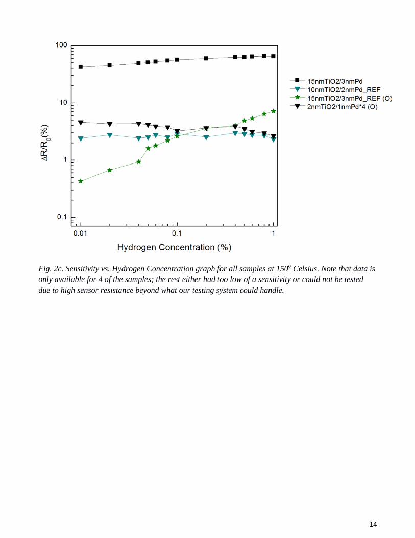
Fig. 2c. Sensitivity vs. Hydrogen Concentration graph for all samples at 150o Celsius. Note that data is only available for 4 of the samples; the rest either had too low of a sensitivity or could not be tested due to high sensor resistance beyond what our testing system could handle.

15
Fig. 2d. Response Time vs. Hydrogen Concentration graph for all samples at 150o Celsius. Note that data is only available for 4 of the samples; the rest either had too long of response times or could not
be tested due to high sensor resistance beyond what our testing system could handle.

16
Fig. 3a. Bar graph of sensitivities of selected sensors at a hydrogen concentration of 1%. The 15 nm TiO2/3 nm Pd sample is much more sensitive than any other sample.

17
Fig. 3b. Bar graph of response times of selected sensors at a hydrogen concentration of 1%. The 15 nm
TiO2/3 nm Pd sample is several seconds quicker than any other sample.

18
Fig. 4a. Sensitivity vs. Concentration graph for the 15 nm TiO2/3 nm Pd sample. The graph shows that this sensor was over 10 times more sensitive at 150o Celsius than at room temperature.

19
Fig. 4b. Response time vs. Concentration graph for the 15 nm TiO2/3 nm Pd sample. The graph shows that this sensor was much quicker at 150o Celsius than at room temperature.

20
Fig. 5a. Sensitivity vs. Concentration graph for the 4-layered 2 nm TiO2/1 nm Pd sample. The graph shows that the sample made with oxygen as part of the working gas had a sensitivity approximately 5 times greater than that made without oxygen, and almost 10 times greater than the thin film reference
sample.

21
Fig. 5b. Response time vs. Concentration graph for the 4-layered 2 nm TiO2/1 nm Pd sample. Similar to Figure 5a,the sample made with oxygen as part of the working gas generally has a shorter response
time than either of the reference samples or the sample made with only argon in the working gas.

22
Sources Cited and Consulted 1. Hydrogen Sensor. http://web.anl.gov/techtransfer/pdf/Profile_HydrogenSensor9_06.pdf. Accessed
June 25, 2013 2. Zeng, X.Q.; Latimer, M.L.; Xiao, Z.L.; Panuganti, S.; Welp, U.; Kwok, W.K.; Xu, T. Nano Lett.
2011, 11, 262-268. 3. Kim, K.T.; Sim, S.J.; Cho, S.M. IEEE Sensors Journal 2006, 6, 509-513. 4. Lee, E.; Lee, J.M.; Koo, J.H.; Lee, W.; Lee, T. International Journal of Hydrogen Energy 2010, 35,
6984-6991. 5. Hübert, T.; Boon-Brett, L.; Black, G.; Banach, U. Sens. Actuators B 2011, 157, 329-352. 6. Buttner, W.J.; Post, M.B.; Burgess, R.; Rivkin, C. Int. J. Hydrogen Energy 2011, 36, 2462-2470. 7. Amyotte, P.; Rigas, F. Chemical Engineering Transactions 2013, 31. 8. Yang, F.; Kung, S.C.; Cheng, M.; Hemminger, J.C.; Penner, R.M. ACS NANO 2010, 4, 5233-5244. 9. Zeng, X.Q.; Wang, Y.L.; Deng, H.; Latimer, M.L.; Xiao, Z.L.; Pearson, J.; Xu, T.; Wang, H.H.;
Welp, U.; Crabtree, G.W.; Kwok, W.K. ACS NANO 2011, 5, 7443-7452. 10. Kim, K.R.; Noh, J.S.; Lee, J.M.; Kim, Y.J.; Lee, W. J Mater Sci. 2011, 46, 1597-1601. 11. Zeng, X.Q.; Wang, Y.L.; Xiao, Z.L.; Latimer, M.L.; Xu, T.; Kwok, W.K. J Mater Sci. 2012, 47,
6647-6651. 12. Lee, E.; Lee, J.M.; Lee, E.; Noh, J.S.; Joe, J.H.; Jung, B.; Lee, W. Thin Solid Films 2010, 519, 880-
884. 13. Fields, L.L.; Zheng, J.P.; Cheng, Y.; Xiong, P. Applied Physics Letters 2006, 88