Report of the improved SON of EDGAR - Mechanical...
76
Report of the improved SON of EDGAR by Jan Bennik
Transcript of Report of the improved SON of EDGAR - Mechanical...

Report of the improved SON of EDGAR
by
Jan Bennik

Preface
For my Masters of Mechanical Engineering and Automation at the University of Twente in the Netherlands, a traineeship is compulsory in order to obtain a Master of Engineering degree. Rather than undertaking a traineeship in the Netherlands, I searched for a place in Australia. Via Dick Petersen, an old student of the University of Twente, I came in contact with Assoc. Prof. Dr. Ben Cazzolato. He gave me the possibility to do my traineeship at the School of Mechanical Engineering at the University of Adelaide.
This report describes the work I have undertaken on a self balancing scooter named SON of EDGAR.
I would like to thank everybody who helped me with making my traineeship possible. Special thanks go out to the people that contributed their valuable experience, knowledge and support that made this report possible:
• Assoc. Prof. Dr. Ben Cazzolato
• Mr. Philip Schmidt
• Mr. Steven Kloeden
• Mr. Zebb Prime
• Mr. Jayesh Minase
I also would like to thank the University of Twente for giving me the opportunity to come to Australia and do my traineeship at the University of Adelaide.
The improved SON of EDGAR
i
Preface
i

Summary
This report describes improvements made to an already existing self balancing scooter named SON of EDGAR, made by the University of Adelaide. This scooter is a second version of the 4th years honours project EDGAR. Despite the experience from the EDGAR project, the SON of EDGAR still had some minor and major problems.
The most important results of this traineeship are the improvements of the electronics of the SON of EDGAR which are shown in Figure 1. This shows the improvement in the wiring and electronics made during the traineeship.
Figure 1: Photographs of the interior wiring of SON of EDGAR before and after modifications
The background of the EDGAR and SON of EDGAR projects and the problems that were faced, are described in Chapter 1. Also the problem description and the project focus made for this traineeship can be found in this chapter.
Chapter 2 addresses the mechanical failure of the SON of EDGAR. This failure was the broken handle bar coupling and was due to a bad design and inappropriate choice of material.
After the mechanical failure was fixed the initial test ride could be made. But it was noticed that there were also some electronics issues and some other minor failures. What these problems were and how these problems were solved is described in Chapter 3.
With the scooter now functional, the improvements were committed. The major changes are in the electronics of the SON of EDGAR. This because the existing electronics were not save or reliable anymore. The most important change made is the PWM controller, used for driving the motors in the SON of EDGAR. From all the electronics is a brief description given in Chapter 4 as well the made changes are mention.
Because of the changes made in the electronics and the hardware of the scooter, the old SIMULINK model no longer worked. A new SIMULINK model was made for driving all the hardware and the electronics on the SON of EDGAR. The most important issues of this model are explained in Chapter 5.
With the changes to the hardware and the software of the SON of EDGAR, the first test ride of the new SON of EDGAR could be made. The test procedure and the results of these test are given in Chapter 6. How the problems are solved that were faced during the testing is also described in this chapter.
After the tests and some adjustments, the SON of EDGAR was working properly. But there was still a problem with an audible noise produced by the PWM signal in the motors. Because this noise was to large to ignore it was decided to try some different approaches of producing the PWM signal.These approaches are described in Chapter 7.
The improved SON of EDGAR
2ii
Summary

In Chapter 8 the conclusions are given that are made during this traineeship of the improving of the SON of EDGAR .
The last chapter gives some recommendations for future work with the SON of EDGAR. These recommendations could improve, when implemented, the SON of EDGAR more.
The improved SON of EDGAR
iii
Summary

Table of Contents
1. ........................................................................................Introduction 1
1.1. ........................................................................................................Project background 1
1.2. ..........................................................................Problem description and project focus 1
2. ....................................................................Redesign of the handle bar 3
3. ..........................................................Initial test ride of SON of EDGAR 5
4. ..........................................................................................Electronics 7
4.1. ....................................................................................................................Minidragon 7
4.2. ...................................................................................................New PWM controller 10
4.3. ...............................................................................................................New taillights 13
4.4. ........................................................................................................New power supply 14
4.5. ....................................................................................................New battery monitor 15
4.6. .....................................................................................New power distribution board 16
4.7. .................................................................................................................RS232 ports 17
5. ...............................................................................SIMULINK model 18
5.1. .....................................................................................................................Controller 18
5.2. ........................................................................................Automatic battery drop bias 20
5.3. ......................................................................................................................Taillights 20
5.4. ..................................................................................................PWM to bit converter 22
6. ..............................................................................................Testing 23
6.1. ...................................................................................................................New biases 23
6.2. ...........................................................................................Testing of the minidragon 23
6.3. ....................................................................................Testing of the PWM controller 24
6.4. ............................................................................Testing of the controller and model 26
6.5. ...............................................................................Test ride on the SON of EDGAR 27
7. .......................................................................................Final design 28
7.1. .................................................................................................................New crystals 28
The improved SON of EDGAR
4iv
Table of contents

7.2. ...................................................................................................New PWM approach 28
8. ........................................................................................Conclusion 32
9. ..............................................................................Recommendations 33
9.1. ..................................................................................................Backlash free gearbox 33
9.2. .................................................................Enabled encoders for closed loop feedback 33
9.3. .........................................................................................Proper system identification 33
9.4. ..........................................................................Adding a gyroscope in the yaw plane 33
.........................................................................................References 34
A. ..................................................................................Appendix 35
A. ..................................................................................................................Experiments 35
A.1 ...............................................................................................................Fan Plate 35
A.2 ........................................................................................Floating ping pong ball 41
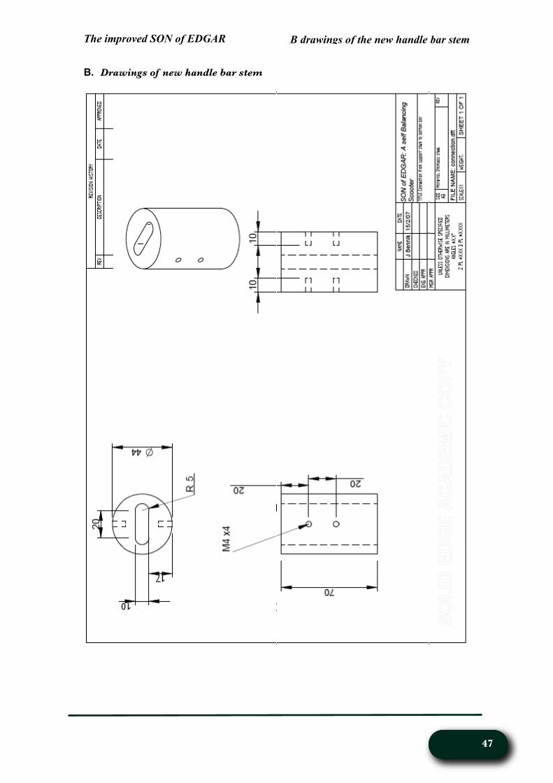
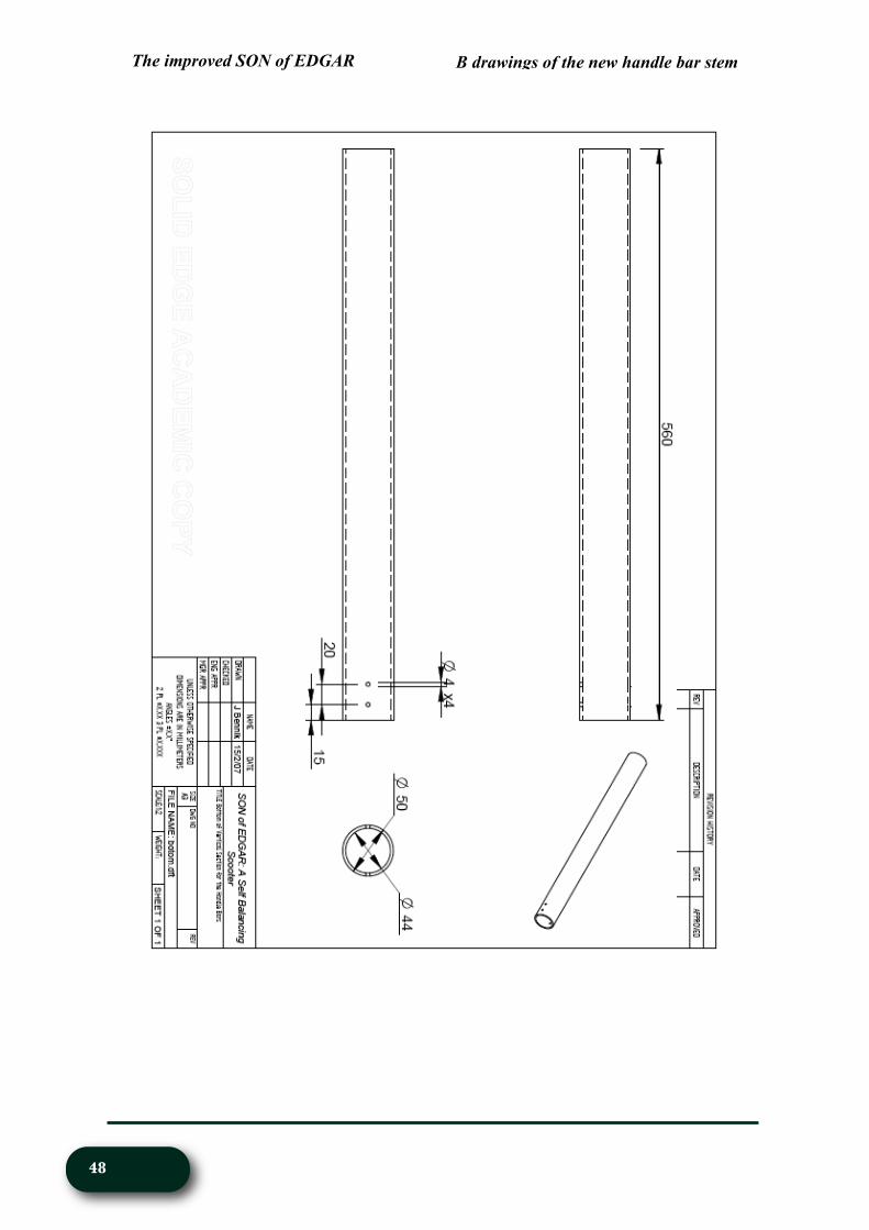
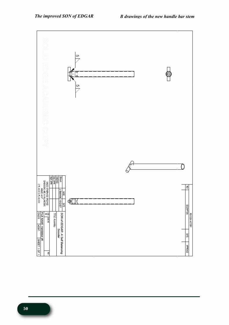
B. ................................................................................Drawings of new handle bar stem 47
C. ......................................................................................................Features minidragon 51
D. ................................................Map of minidragon board with port and pin numbers 54
E. ......................................................................................................Electronic diagrams 55
F. ...............................................................................................C. code PWM controller 61
G. ...................................................................................Specifications DC DC converter 63
H. ............................................................................................................Wiringdiagrams 64
I. .........................SIMULINK model SON of EDGAR with separate PWM controller 68
J. ....................................................................................................PWM to bit converter 69
K. ...........................................................................SIMULINK model with optocoupler 70
The improved SON of EDGAR
v
Table of contents
1 Introduction
The work that was undertaken for this traineeship aimed to improve an already existing self balancing scooter made by the School of Mechanical Engineering at the University of Adelaide. In Section 1.1 a short description is given on the background of the project and the work already done. Section 1.2 gives a problem description and a project focus for this traineeship.
1.1 Project background
In December 2001 inventor Dean Kamen unveiled the Segway PT (personal transportation), a two-wheeled, self balancing scooter. The user of the Segway PT can ride it by leaning forwards to ride forward and leaning back to ride backwards. Gyroscopes detect when the scooter is unbalanced and a computer drives the electric motors to balance the scooter again or to ride forwards or backwards.
As an answer on this new transportation form, the Segway PT, the School of Mechanical Engineering of the University of Adelaide came up in 2005 with EDGAR, which stands for Electro-Drive Grav-Aware Ride, and like the Segway PT is also a self balancing scooter.
Because not all of the extended goals of this project were accomplished, it was decided by the School of Mechanical Engineering at the University of Adelaide to run a new project in 2006. This project was to address all of the shortcomings of the EDGAR project. The project was called SON of EDGAR. This new name stands for State Space Control of Electro Drive Gravity Aware Ride.
The SON of EDGAR became an easy scooter to ride on, in contrast to EDGAR. But despite the experiences with the EDGAR project, not all goals were achieved with the SON of EDGAR project. During the process of developing the SON of EDGAR new problems and shortcomings became apparent. This was especially due to the time pressure that was created by the deadline for the exhibition. Addressing these problems and shortcomings became the goals for this traineeship.
1.2 Problem description and project focus
The primary goals for the former project of the SON of EDGAR were:
1. To develop an accurate and robust mathematical model of the system.2. Convert the mathematical model into a state space plant.3. Analyse the state space model in ‘MATLAB’ and ‘Simulink’.4. Implement closed loop steering and balancing.5. Design and build a physical prototype.6. Create virtual reality model.7. Run the prototype tethered, on a computer, using the on board micro controller.8. Implement a BleutoothTM communication system.
The first 7 goals were achieved during the project, except that it seemed not possible to design a working controller with the mathematical model of the system. For that reason the controller for the SON of EDGAR was tuned by trial and error. The controller used for steering is an open loop controller because the encoders that were intend to provide feedback on rotational speed were never implemented. Nevertheless seemed this controller to work sufficient. The BleutoothTM communication system was also never implemented.
The improved SON of EDGAR
1
1 Introduction
1

Soon after the exhibition the handle bar broke in two parts. Also the potentiometer that is used for steering no longer worked. Because of the time pressure in which the SON of EDGAR was built, a lot of the electronic parts were made in a rush. This resulted in a complex way wherein the electronic parts were organised. In addition many of the circuit boards were fixed with only pieces of tape as an interim measure. Other things that were not implemented were the brake lights and the indicators. The last thing that was missing was a proper documentation of the electronics and the hardware.
When the SON of EDGAR was tested it seemed that when the battery voltage dropped the scooter began to tilt because the native horizontal position, according to the accelerometer, was shifted due to a supply voltage bias.
To solve all these problems the following goals for this traineeship are described as follows:
1. New design for the handle bar that is stronger and more durable than the old one.2. Rearrange and redesign the circuit boards to make it clearer and more synoptic.3. Documentation of the circuit boards and wiring diagrams. 4. Implement the brake lights and indicators.5. Implement the complementary filters. The analog electronics drifts with supply
voltage.6. New SIMULINK model with a PD controller.7. Testing of the SON of EDGAR.
The solution of all these goals are described in the following chapters. The sequence used for describing the goals is not necessary the same as the sequence of the chapters.
The improved SON of EDGAR
2
1 Introduction

2 Redesign of the handle bar
During the usage of the SON of EDGAR the support stem for the handle bar (Figure 2.1) was broken into two parts. This was due to a weak assembly and the inappropriate choice of material for this purpose. The original support stem was made of aluminium and was directly welded to the vertical section of the handle bar, that also was made out of aluminium. A weld of an aluminium connection is quite weak, which eventually failed as shown in Figure 2.2.
Figure 2.1: New designed handle bar
Figure 2.2: Broken handle bar support stem
Consequently a new handle bar had to be made. The handle bar was improved by using a stainless steel support stem instead of an aluminium one. Also the design of the handle bar was improved. On the new support stem is a short tube welded, like a T-connection. The
The improved SON of EDGAR
33
2 Redesign of the handle bar
Steering potentiometer
LED power indicator
Support stem
Clamp to adjust the height

short tube was also made out of stainless steel. The advantage of stainless steel compared to aluminium is that it can be welded with a weld that is much stronger than a weld made of aluminium.
The vertical section of the aluminium handle bar is attached with a press fitting over the small connection tube. To prevent shearing between the short tube and the vertical section of the handle bar, four M4 bolts are used to screw the to parts together. To increase the friction of the support stem for better clamping, a knurled surface is used at the ends of the support stem. The drawings of the new redesigned handle bar can be found in Appendix B. Figure 2.3 shows the new support of the handle bar.
Figure 2.3: New support stem handle bar
The improved SON of EDGAR
4
M4 Bolts Aluminium handle bar stem
Stainless steel tube
Stainless steel support stem
Knurling
2 Redesign of the handle bar

3 Initial test ride of SON of EDGAR
After repairing the broken handle bars, it was noticed that some wires were lose. These were the wires of the steering potentiometer (Figure 2.1) in the handle bar. Without these wires it was not possible to steer or to ride on the SON of EDGAR. The reason for the looseness in the wires was because the wiring loom was made too short, which resulted in pulling of the loom whenever the handle bar was removed. So before a test ride on the SON of EDGAR could be made this problem had to be addressed first.
The lengths of the wires were increased by soldering another piece of wire at the existing wires. The solder was covered by a piece of heat-shrink, to prevent it from coming in contact with each other and to cause a short.
After the wires were repaired it was found out that the bias of the steering potentiometer was set incorrectly. To overcome this problem temporarily, without adjusting the SIMULINK model, a separate potentiometer with a maximum of 10 KΩ was used to set the bias of the steering potentiometer manually. The potentiometer was connected with the ground cable of the steering potentiometer and with a positive voltage wire.
After these wires were soldered together (Figure 3.1), the SON of EDGAR was assembled together again. When this was done the first test ride could be done. This ride was successful, except that the tires were flat. Pumping the tires up solved this problem.
Figure 3.1: New soldered wires
Despite that the SON of EDGAR was running, there were still several hardware issues. This was due to the fact that the assembly of the SON of EDGAR by the previous group was done in a short period. During this period some problems came up and these were fixed by short-term solutions.
These problems had to be fixed to guarantee a safe drive on the SON of EDGAR. Although the most of the sort-term solutions worked, it was not very safe to drive on the SON of EDGAR. Many parts were fixed by tape only or were simply lose in the case as shown in Figure 3.2.
The improved SON of EDGAR
55
3 Initial test ride SON of EDGAR

Figure 3.2: Photograph showing the original wiring inside the SON of EDGAR
The chance that some parts could cause shorts or simply break was high. This was also noticed during the test ride when the SON of EDGAR suddenly did not respond anymore and threw the rider off the scooter.
Another problem were the capacitive sensors. The cables of these sensors were made too short. Also, the sensors were only attached with tape to the platform. Because of the inadequate length of the wires, before the platform could be removed the sensors had to be removed first. To solve this problem, the cables were made longer so the sensors could be screwed onto the platform permanently. When the platform has to be removed the sensors can still be connected to the platform because of the length of the new cables. Also a new mechanism to wind the cables direct on the platform is integrated in the platform. This mechanism is shown in Figure 3.3.
Figure 3.3: Cable winding mechanism for the capacitive sensors
The improved SON of EDGAR
6
Left capacitive sensor
Right capacitive sensor
Loom
3 Initial test ride SON of EDGAR

4 Electronics
To improve the clarity and reliability of the electronic circuits in a much more open manner than the previous attempt, all the old electronics were replaced by new electronics. New circuits boards were designed and fabricated. The new circuit boards were connected to each other with new wiring. These wires were chosen for functionality and clarity (thickness and colour) and were layered out in a much more open manner than the previous attempt. New colour maps for the wiring and diagrams for the electronic part of the SON of EDGAR have been made. The following sections explain all the electronics on the SON of EDGAR and the adjustments made.
4.1 Minidragon
The most important component of SON of EDGAR is its ‘brain’, or the micro-controller. For SON of EDGAR the minidragon board is used as shown in Figure 4.1. The minidragon is a relative cheap board employing a Freescale (Motorola) HC 512 chip with a high functionality.
The features of the minidragon board are given in Apendix C. The mean features for the communication are the RJ 11 handset jack and the pins on the board.
The pins on the boards, may be used as inputs or outputs. The outputs are used to control the components as the motor controller or the LED’s in the handle bar in the SON of EDGAR. They can also be used as an input to send information from the sensors to the microprocessor on the minidragon board to process the data.
Figure 4.1: Minidragon board
Every pin on the minidragon board is numbered. These numbers represent a port. This can be an ADC, digital input or a digital output port. Every specific input and output used for driving the SON of EDGAR can be found in Table 4.1 and 4.2. The drawing of the minidragon board with the associated ports can be found in Appendix D.
The improved SON of EDGAR
77
4 Electronics
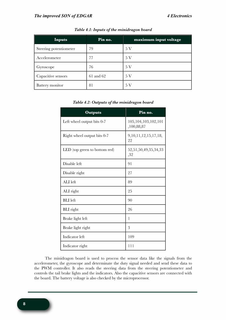
Table 4.1: Inputs of the minidragon board
Inputs Pin no. maximum input voltage
Steering potentiometer 79 5 V
Accelerometer 77 5 V
Gyroscope 76 5 V
Capacitive sensors 61 and 62 5 V
Battery monitor 81 5 V
Table 4.2: Outputs of the minidragon board
Outputs Pin no.
Left wheel output bits 0-7 105,104,103,102,101,100,88,87
Right wheel output bits 0-7 9,10,11,12,15,17,18,22
LED (top green to bottom red) 52,51,50,49,35,34,33,32
Disable left 91
Disable right 27
ALI left 89
ALI right 25
BLI left 90
BLI right 26
Brake light left 1
Brake light right 3
Indicator left 109
Indicator right 111
The minidragon board is used to process the sensor data like the signals from the accelerometer, the gyroscope and determinate the duty signal needed and send these data to the PWM controller. It also reads the steering data from the steering potentiometer and controls the tail brake lights and the indicators. Also the capacitive sensors are connected with the board. The battery voltage is also checked by the microprocessor.
The improved SON of EDGAR
8
4 Electronics

All these signals are read with a sampling time of 0.01 sec. In other words the frequency of the minidragon board is 100 Hz. When the frequency of the minidragon is set to a higher frequency, the buffer of the minidragon overflows for the particular SIMULINK model employed and the SON of EDGAR becomes unstable.
Figure 4.2: Adjusted minidragon board
To reduce the space occupied by the electronics within the SON of EDGAR the redundant breadboard was removed by sawing these off the board (Figure 4.2).In the new design, the power supply was directly soldered on to the board instead of using a plug, which also results in more space. Figure 4.3 shows the map with the connections of the wires from and to the board used in the new design. Behind the descriptions (see Figure 4.3) of the wire stands the colour of that wire.
Figure 4.3: Connections map for new micro-controller
The improved SON of EDGAR
99
4 Electronics
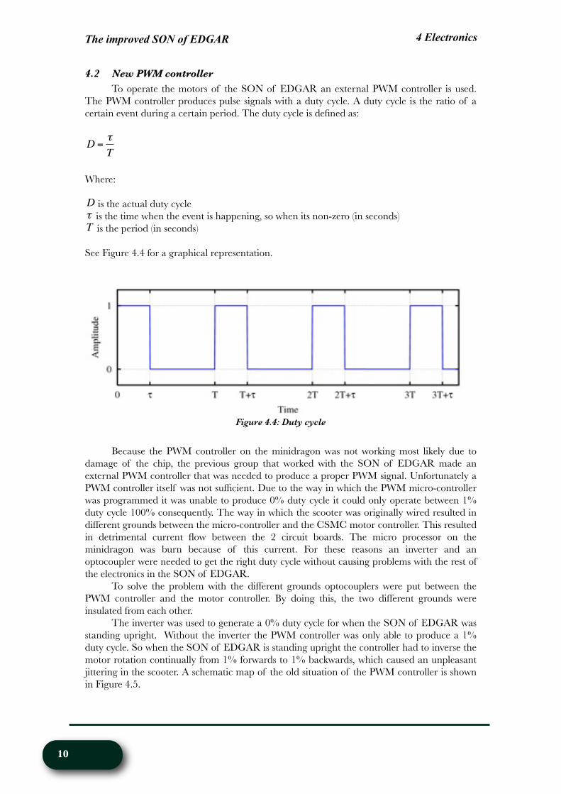
4.2 New PWM controller
To operate the motors of the SON of EDGAR an external PWM controller is used. The PWM controller produces pulse signals with a duty cycle. A duty cycle is the ratio of a certain event during a certain period. The duty cycle is defined as:
€
D =τT
Where:
€
D is the actual duty cycle
€
τ is the time when the event is happening, so when its non-zero (in seconds)
€
T is the period (in seconds)
See Figure 4.4 for a graphical representation.
Figure 4.4: Duty cycle
Because the PWM controller on the minidragon was not working most likely due to damage of the chip, the previous group that worked with the SON of EDGAR made an external PWM controller that was needed to produce a proper PWM signal. Unfortunately a PWM controller itself was not sufficient. Due to the way in which the PWM micro-controller was programmed it was unable to produce 0% duty cycle it could only operate between 1% duty cycle 100% consequently. The way in which the scooter was originally wired resulted in different grounds between the micro-controller and the CSMC motor controller. This resulted in detrimental current flow between the 2 circuit boards. The micro processor on the minidragon was burn because of this current. For these reasons an inverter and an optocoupler were needed to get the right duty cycle without causing problems with the rest of the electronics in the SON of EDGAR.
To solve the problem with the different grounds optocouplers were put between the PWM controller and the motor controller. By doing this, the two different grounds were insulated from each other.
The inverter was used to generate a 0% duty cycle for when the SON of EDGAR was standing upright. Without the inverter the PWM controller was only able to produce a 1% duty cycle. So when the SON of EDGAR is standing upright the controller had to inverse the motor rotation continually from 1% forwards to 1% backwards, which caused an unpleasant jittering in the scooter. A schematic map of the old situation of the PWM controller is shown in Figure 4.5.
The improved SON of EDGAR
10
4 Electronics
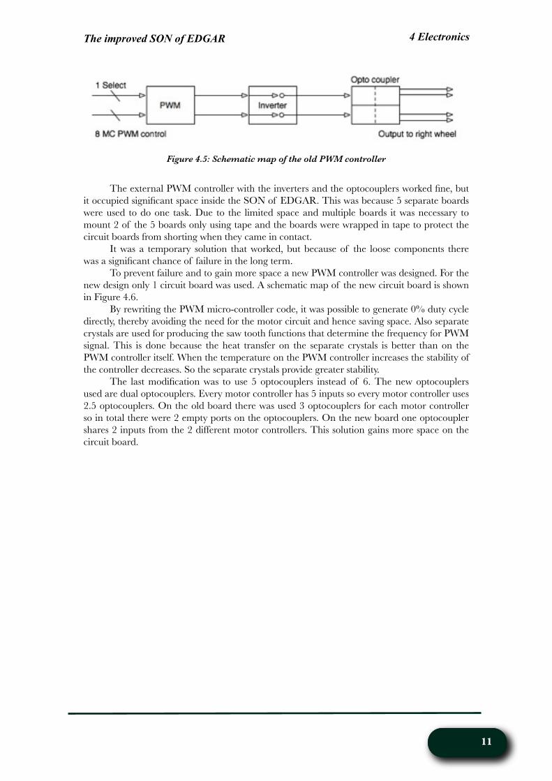
Figure 4.5: Schematic map of the old PWM controller
The external PWM controller with the inverters and the optocouplers worked fine, but it occupied significant space inside the SON of EDGAR. This was because 5 separate boards were used to do one task. Due to the limited space and multiple boards it was necessary to mount 2 of the 5 boards only using tape and the boards were wrapped in tape to protect the circuit boards from shorting when they came in contact.
It was a temporary solution that worked, but because of the loose components there was a significant chance of failure in the long term.
To prevent failure and to gain more space a new PWM controller was designed. For the new design only 1 circuit board was used. A schematic map of the new circuit board is shown in Figure 4.6.
By rewriting the PWM micro-controller code, it was possible to generate 0% duty cycle directly, thereby avoiding the need for the motor circuit and hence saving space. Also separate crystals are used for producing the saw tooth functions that determine the frequency for PWM signal. This is done because the heat transfer on the separate crystals is better than on the PWM controller itself. When the temperature on the PWM controller increases the stability of the controller decreases. So the separate crystals provide greater stability.
The last modification was to use 5 optocouplers instead of 6. The new optocouplers used are dual optocouplers. Every motor controller has 5 inputs so every motor controller uses 2.5 optocouplers. On the old board there was used 3 optocouplers for each motor controller so in total there were 2 empty ports on the optocouplers. On the new board one optocoupler shares 2 inputs from the 2 different motor controllers. This solution gains more space on the circuit board.
The improved SON of EDGAR
1111
4 Electronics

Figure 4.6: Schematic map of the new PWM controller
The final design of PWM controller board is shown in figure 4.7.
(a) Top view (b)Bottom view
Figure 4.7: Final PWM board
The PWM controller, shown in Figure 4.7 has 12 inputs and 5 outputs per motor. The inputs on the boards are of 8 different bits, ALI, BLI, select and the disable. The outputs are AHI, BHI, ALI, BLI and the disable (total 12 ports). All these output signals are directly connected with the motor controller board. The inputs of the motor controllers are defined following Table 4.1. The code used for programming the PWM controller can be found in Appendix F.
The improved SON of EDGAR
12
4 Electronics

Table 4.1: Motor controller schematic
Direction AHI BHI ALI BLI Disable
Forward PWM 0 0 1 0
Backward 0 PWM 1 0 0
Stop x x x x 1
x=don’t care
4.3 New taillights
For safety and aesthetic reasons the SON of EDGAR is equipped with taillights. The Son of EDGAR has 2 taillights, one on each side. The taillights are comprised of a brake light on the outside and an indicator on the inside of the tail lights. The brake lights are supposed to glow at 10% when the SON of EDGAR is accelerating and to glow at 100% when it is decelerated. This is done because of safety, so that people who are behind the scooter can see when the scooter stands still or is decreasing speed.
The indicators are used to warn others when the SON of EDGAR is turning and in which direction. These indicators react on the steering potentiometer wiper. When turning left the left indicator blinks, when turning right the right indicator blinks.
The taillight boards were redesigned. New LED’s where used with greater brightness and the complete board is photolithographically etched on a PCB instead of separate wires. The new wiring to the distribution board now employs a header. This makes it easier to uncouple the taillights when the fenders are removed. The new and the old taillights are shown in Figure 4.8.
Figure 4.8: Original taillight is shown in left the new taillight board is shown in the right
The improved SON of EDGAR
1313
4 Electronics

4.4 New power supply
Instead of connecting the power supply cables for all the boards directly to the batteries, an active and a neutral bar has been used in the new design. The terminal bars have the advantage that it is much clearer which cable is used for the positive voltage and which one is used for the ‘negative’ voltage or ground. Also the connector on the battery is ‘cleaner’ because there is only one cable connected to each battery terminal.
The fuses for the motor controllers have been placed between the active and the neutral bar are. These are 40A fuses. It is also possible to connect some more components to the bars if needed in the future as there are still 3 connections unused.
Each of the bars contains the following 4 cables:
1.Input from batteries2.Motor controller left3.Motor controller right4.Power distribution board
A photo of the active and neutral bars with the new power supply wiring is shown in Figure 4.9.
Figure 4.9: New power supply terminal blocks
Not only are the new terminal bars used but all the power cables were replaced and were fixed to the inside of the case. Where the wires exit the electronics case to drive the motor, the holes were lined with grommets as shown in Figure 4.10. This was done to prevent damage to the insulation of the wires.
Figure 4.10: Hole with covered edges
The improved SON of EDGAR
14
4 Electronics
Active 3 unused connectors
Active used connectors Earth used connectors
Earth 3 unused connectors

4.5 New battery monitor
To monitor voltage changes in the batteries, a separate battery monitor device is used. This battery monitor is a separate board. This in contrast to the old one. The old one were just 2 lose resistors plugged into the extra sockets on the minidragon as shown in Figure 4.11.
Figure 4.11: Old battery monitor
The battery monitor is in fact just an voltage divider. This divider is comprised of 2 resistors with a resistance 4.7kΩ and 1.0kΩ. This means when the batteries are charged and providing 24V the output of the battery monitor is:
€
Voutput =Rb
Ra + Rb
⋅Vinput
10004700 +1000
⋅ 24 = 4.21V
When the battery voltage drops during the use, the output of the battery monitor also drops. The output of the monitor is used for feedback to the current input into the motors. Which explained later in Chapter 5.
The output of the battery monitor is plugged to the ground of the minidragon board and into pin number 81 on the minidragon board. The resistors were chosen so that the output is never higher than 5V, which is the maximum input voltage of the minidragon. The new battery monitor board is shown in Figure 4.12.
Figure 4.12: New battery monitor
The improved SON of EDGAR
1515
4 Electronics
2 Lose resistors

4.6 New power distribution board
There are 4 different voltages needed to power all the components in the SON of EDGAR as shown in table 4.2.
Table 4.2: Power distribution board
Voltage Components
1 5V Potentiometer, Gyroscope, Accelerometer, Handle bar LED’s
2 9V Minidragon
3 18V Capacitive sensors
4 24V Tail lights
All these voltages are distributed by a single board, called the power distribution board. The input to this board is the 24V directly from the batteries. On the board this voltage is divided into the 3 other needed voltages.
Immediately after the power input a diode was placed. This was done to prevent the current flowing back to the batteries when the voltage is dropping. For example when the rider is moving from forwards to backwards. At this point the motors are going from a maximum power to zero and back to maximum.
A 5A fuse is used to secure the board from external shorts or a too high current. This fuse used to be together with the 40A fuses of the motor controller. But the sockets that are used for these fuses are quit big. To gain more space the 5A fuse is put on the power distribution board.
A relatively large capacitor, of 10000 µF, is used for when the voltage is dropping fast when the motors are suddenly drawing a high current from the batteries. This is done to smooth out transients.
To provide the 5V, a DC DC converter is used of the type SLW05-05. The specifications of this converter can be found in Appendix F. The 9V and the 18V supply is provided by a voltage divider using resistors.
On the power distribution board are also 3 LED’s. These LED’s are used for checking if the 3 different voltages are being distributed and if the power distribution board is working properly.
The improved SON of EDGAR
16
4 Electronics

Figure 4.13: Power distribution board
Figure 4.13 shows the new power distribution board. Not only the power is distributed on this board but also the gyroscope is mounted on the board. The gyroscope is put in the corner of the board because it is fixed here to the SON of EDGAR, thus the deflection here is the smallest when the board is subject to vibration. The gyroscope is mounted in line with the tilt angle of the scooter. According to the sensor, moving backwards results in a positive voltage and moving forwards leads to a negative voltage.
4.7 RS232 ports
The communication between the host computer used to program the minidragon is done via RS232 communication. Two different RS232 connectors are needed for the SON of EDGAR. The first one is the connector that send data from the computer to the minidragon, the second one sends data from the minidragon back to the computer. This can be done in order to enable observation of data values, permitting system identification.
To facilitate remove of the foot plate the RS232 connectors have been mounted at the rear of the scooter as shown in Figure 4.14.
Figure 4.14: The RS232 ports
The improved SON of EDGAR
1717
DC DC converter24V power input
5A Fuse
Gyroscope
Diode
FET
Darlington transistor array
Data out
Data in
4 Electronics

5 SIMULINK model
In order to increase the stability of the SON of EDGAR a new SIMULINK model is made. The following sections highlight the most important changes made in the already existing model made by the previous group. The control of riding in these sections is done in an open loop, because there is no feedback from the motors. The control of the balancing is done in closed loop control, because of the feedback from the sensors. The complete SIMULINK model of the SON of EDGAR can be found in Appendix H.
5.1 Controller
The controller that is used for the SON of EDGAR contains three different control types:
1. proportional gain2. derivative gain3. quadratic controller
The proportional gain is used to increase the response from the sensors to the motors. For this gain the same value is used as it was set by the previous group. The value of the proportional gain is 4. The unit of
€
θ is radians. The equation for the proportional gain is:
€
Dutyproportional = 4 ⋅ θ
The derivative gain was not used before. Adding this gain was done with the intention that a derivative gain would add additional damping to the system. This damping should make the SON of EDGAR more smooth in the equilibrium. The initial value of the derivative gain was chosen to be 1. In order to alleviate the high frequency amplification in the total PD controller, a low pass filter was used. The cut off frequency was 60 rad/s, with a time constant τp of 1/60. The derivative controller is given in the following equation.
€
Dutyderivative =s
160 ⋅ s+1
⋅ θ
A sliding controller is an quadratic controller. This controller type is added for adaptive control dependent of the pitch angle. In other words when the pitch angle increases the controller becomes more ‘aggressive’ and automatically increases the gain quadratically. At small angles the controller gain changes are not dramatic. For this reason, when the rider is balancing uptight the sensitivity stays relatively small. But for large angles the sensitivity increases quadratically, which results in a faster response. The gain for the sliding controller is also taken the same as the old one, the sliding controller gain is 8. The equation for this sliding controller is:
€
Dutyquadratic = 8 ⋅ θ 2
The total equation that represents the controller is given by:
The improved SON of EDGAR
18
5 SIMULINK model

€
Dutytotal = 4 ⋅ θ +s
160 ⋅ s+1
⋅ θ + 8 ⋅ θ 2
The equation for the controller per motor is given as:
€
Dutytotal = 0.5 ⋅ (4 ⋅θ +s
160 ⋅ s+1
⋅ θ + 8 ⋅ θ 2)
This equation is implemented in SIMULINK as shown in figure 5.1.
VoltsVolts Deg/s rad/s
Volts
radians
Send in 0-20 for angle -1 to 1 radSend in 0-4 for pot
angle error
Volts
Volts
Volts radians
Volts VoltsVolts Volts
radianstheta
Vp
Vq
Vd
V
-3.25
potentiometer bias voltage
Zero-OrderHold1
asin
TrigonometricFunction
Subtract4
Subtract3
Subtract2Subtract1
Subtract
In1Right brake light
Left brake light
Subsystem2
In1Right Indicator
Left Indicator
Subsystem1
Battery Voltage
Filtered Battery Voltage
Gain
Subsystem
Sign
Saturation3
Saturation2
Saturation1
PORTBPins: 1,2,3
Right motor controller
ON/OFF
Voltage
ALI
BLI
DISABLE
Switch
RIGHT1
Switch
duty in
RIGHT
8
Quadratic gain angle (rad)
-.15
Proportional gain4
.15
Proportional gain3
.5
Proportional gain2
.5
Proportional gain1
4
Proportional gain
Product3
Product2
Product1
Product
1
.01s+1
Potentiometer low pass filter
ADC InputChannel 6
Potentiometer
2/1.54
Pot Gain
Pulse pin: PTP.5Sign pin: PTP.4
Period: 1 (s)PWM right indicator
Pulse pin: PTP.5Sign pin: PTP.4
Period: 1 (s)PWM right indicator
Pulse pin: PTP.5Sign pin: PTP.4
Period: 1 (s)PWM right indicator
Pulse pin: PTP.5Sign pin: PTP.4
Period: 1 (s)PWM right indicator
PWM-B, 16-bitPulse pin: PTP.3Sign pin: PTP.2
Period: 1e-005 (s)Saturation: 1PWM right breaklight
Pulse pin: PTP.7Sign pin: PTP.6
Period: 1 (s)PWM left indicator
Pulse pin: PTP.1Sign pin: PTP.0
Period: 0.0001 (s)PWM left breaklight
AND
LogicalOperator
PTSPins: 4,5,6
Left motor controller
Voltage
ON/OFF
Switch
ALI
BLI
DISABLE
LEFT1
duty in
Switch
LEFT
Battery Voltage
LED1
LED2
LED3
LED4
LED5
LED6
LED7
LED8
Handlebar LEDS
ADC InputChannel 4
Gyroscope
-1/.005
Gyro sensitivity2.470
Gyro bias @ 0 rad/s
100s
100s +20s+12
Gyro 2nd Order (0.5)1
PORTAPins: 4,5
Foot sensor
PTHPins: 0,1,2,3,4,5,6,7
Digital output4
0
Derivative gain
s
1/60s+1
Derivative
pi/180
Degrees/sec toradians/sec
Dead Zone
ADC InputChannel 7
Battery voltage
Add3
Add
ADC InputChannel 5
Accelerometer2.511
Accelarometer bias 2 0 degrees
20s+1
100s +20s+12
Accel 2nd Order (0.5)1
|u|
Abs1
|u|
Abs
Figure 5.1: Controller in SIMULINK
The total controller is shown in figure 5.2.
VoltsVolts Deg/s rad/s
Volts
radians
Send in 0-20 for angle -1 to 1 radSend in 0-4 for pot
angle error
Volts
Volts
Volts radians
Volts VoltsVolts Volts
radianstheta
Vp
Vq
Vd
V
-3.25
potentiometer bias voltage
Zero-OrderHold1
asin
TrigonometricFunction
Subtract4
Subtract3
Subtract2Subtract1
Subtract
In1Right brake light
Left brake light
Subsystem2
In1Right Indicator
Left Indicator
Subsystem1
Battery Voltage
Filtered Battery Voltage
Gain
Subsystem
Sign
Saturation3
Saturation2
Saturation1
PORTBPins: 1,2,3
Right motor controller
ON/OFF
Voltage
ALI
BLI
DISABLE
Switch
RIGHT1
Switch
duty in
RIGHT
8
Quadratic gain angle (rad)
-.15
Proportional gain4
.15
Proportional gain3
.5
Proportional gain2
.5
Proportional gain1
4
Proportional gain
Product3
Product2
Product1
Product
1
.01s+1
Potentiometer low pass filter
ADC InputChannel 6
Potentiometer
2/1.54
Pot Gain
Pulse pin: PTP.5Sign pin: PTP.4
Period: 1 (s)PWM right indicator
Pulse pin: PTP.5Sign pin: PTP.4
Period: 1 (s)PWM right indicator
Pulse pin: PTP.5Sign pin: PTP.4
Period: 1 (s)PWM right indicator
Pulse pin: PTP.5Sign pin: PTP.4
Period: 1 (s)PWM right indicator
PWM-B, 16-bitPulse pin: PTP.3Sign pin: PTP.2
Period: 1e-005 (s)Saturation: 1PWM right breaklight
Pulse pin: PTP.7Sign pin: PTP.6
Period: 1 (s)PWM left indicator
Pulse pin: PTP.1Sign pin: PTP.0
Period: 0.0001 (s)PWM left breaklight
AND
LogicalOperator
PTSPins: 4,5,6
Left motor controller
Voltage
ON/OFF
Switch
ALI
BLI
DISABLE
LEFT1
duty in
Switch
LEFT
Battery Voltage
LED1
LED2
LED3
LED4
LED5
LED6
LED7
LED8
Handlebar LEDS
ADC InputChannel 4
Gyroscope
-1/.005
Gyro sensitivity2.470
Gyro bias @ 0 rad/s
100s
100s +20s+12
Gyro 2nd Order (0.5)1
PORTAPins: 4,5
Foot sensor
PTHPins: 0,1,2,3,4,5,6,7
Digital output4
0
Derivative gain
s
1/60s+1
Derivative
pi/180
Degrees/sec toradians/sec
Dead Zone
ADC InputChannel 7
Battery voltage
Add3
Add
ADC InputChannel 5
Accelerometer2.511
Accelarometer bias 2 0 degrees
20s+1
100s +20s+12
Accel 2nd Order (0.5)1
|u|
Abs1
|u|
Abs
Figure 5.2: Total model of the controller
The improved SON of EDGAR
1919
5 SIMULINK model

5.2 Automatic battery drop bias
Another innovation of the work undertaken was the automatic battery drop bias. When the battery voltage drops the input power to the motors drops proportionally. To solve this, the battery monitor is used to monitor the batteries and when the battery voltage drops the input value of the duty cycle to the motors automatically increase. Such that the total power delivery remains constant.
The monitor continuously checks the battery voltage for long term decline in potential. Since the voltage could also drop because of a sudden need for current for the motors, the automatic battery drop bias takes an average value over a certain period. In this case the period taken is 60 seconds. The SIMULINK model for the automatic battery drop bias can be found in Figure 5.3. The left half of the model is the low pass filter. The right half calculates the ratio of the nominal voltage (4.5V) to filtered voltage.
2
Gain
1
Filtered Battery Voltage
Zero-OrderHold
Product
1s
Integrator
4.5
Initial voltage value
1/60
Gain2
1/60
Gain1
1
Battery Voltage
Figure 5.3: Automatic battery drop bias in SIMULINK
5.3 Taillights
Two different inputs are used to drive the taillights. One from the steering potentiometer for the indicators and one from the duty cycle after the controller to operate the brake lights. To make the lights glow a PWM signal is generated by the PWM controller on the minidragon board. This PWM signal is driven via a FET to supply to current like the LEDS.
The brake lights glow at a 10% brightness when the scooter is accelerating. A 100% brightness is used when the scooter is decelerating. To make the LED glow at 10%, a duty cycle of 0.1 is used with a frequency of 1000Hz. This means that the lights are on for 0.0001 second every 0.001 second. Because of this short time it appears to the human eye that the LED glows at 10%. The same is done for the 100% brightness. The PWM frequency is the same but the duty cycle is now 100% as shown in Figure 5.4. A working brake light is shown in Figure 5.5.
2
Left breaklight
1
Right breaklight
Switch2
Switch1
>
RelationalOperator1
<=
RelationalOperator
0.1
Constant4
-0.1
Constant3
0.99
Constant2
0
Constant1
0
Constant
1
In1
Figure 5.4: Brake light in SIMULINK
The improved SON of EDGAR
20
5 SIMULINK model

Figure 5.5: The brake light working
For the indicator a logic control is used. The input signal from the steering potentiometer is compared with a constant value of 0.01 and -0.01 as shown in Figure 5.6. This means that when the input voltage is larger than 0.01V the steering potentiometer is moved to the right and the right indicator becomes activated. If the input voltage is smaller than -0.01V the steering potentiometer is moved to the left and the left indicator becomes activated. The constant of 0.2 is the length of the period of which the indicator is on that is send to the PWM controller. A working indicator is shown in Figure 5.7.
2
Left Indicator
1
Right Indicator
Switch2
Switch1
<
RelationalOperator1
>
RelationalOperator 0.2
Period
Ground
-0.01
Constant1
0.01
Constant
1
In1
Figure 5.6: Indicator in SIMULINK
Figure 5.7: The indicator working
The improved SON of EDGAR
2121
5 SIMULINK model
5.4 PWM to bit converter
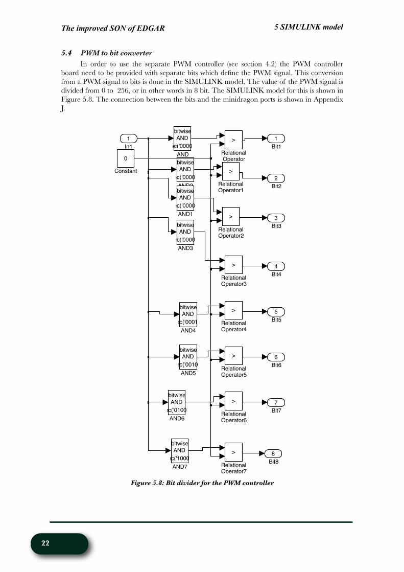
In order to use the separate PWM controller (see section 4.2) the PWM controller board need to be provided with separate bits which define the PWM signal. This conversion from a PWM signal to bits is done in the SIMULINK model. The value of the PWM signal is divided from 0 to 256, or in other words in 8 bit. The SIMULINK model for this is shown in Figure 5.8. The connection between the bits and the minidragon ports is shown in Appendix J.
8
Bit8
7
Bit7
6
Bit6
5
Bit5
4
Bit4
3
Bit3
2
Bit2
1
Bit1
>
RelationalOperator7
>
RelationalOperator6
>
RelationalOperator5
>
RelationalOperator4
>
RelationalOperator3
>
RelationalOperator2
>
RelationalOperator1
>
RelationalOperator0
Constant
bitwise
AND
bin2dec('10000000')
AND7
bitwise
AND
bin2dec('01000000')
AND6
bitwise
AND
bin2dec('00100000')
AND5
bitwise
AND
bin2dec('00010000')
AND4
bitwise
AND
bin2dec('00001000')
AND3
bitwise
AND
bin2dec('00000010')
AND2bitwise
AND
bin2dec('00000100')
AND1
bitwise
AND
bin2dec('00000001')
AND
1
In1
Figure 5.8: Bit divider for the PWM controller
The improved SON of EDGAR
22
5 SIMULINK model
6 Testing
After the new hardware was ready and mounted inside the scooter, the electronics had to be tested to see if the modifications were actually working. When all the new hardware was connected the SON of EDGAR failed to initially work. When it was in equilibrium the wheels were turning and if the scooter was tilted forward or backwards the directions of the wheels violently changed, causing very large impulses. For this reason all the components were tested separately and systematically. The test and the results are described in the following sections.
6.1 New biases
Before starting the real test, the voltage biases of the sensors had to be checked first. This because the biases of the old hardware were used to begin with.
The first bias that had to be changed was the bias of the steering potentiometer. Because the model could be changed now, the extra potentiometer to set the bias manually was removed. To set the bias the SON of EDGAR was put on a crate, so the platform was horizontal or in its equilibrium position. At this point the wheels should not move, when the steering potentiometer was moved to the left the right wheel should turn forwards and the left wheel backwards. When the steering potentiometer was moved to the right the wheels should turn the other way around. Finally a bias of -3.25V was found.
Secondly the biases of the gyroscope and the accelerometer had to be found. This was done with the help of a multi meter. The SON of EDGAR was still standing on the crate, at this point the offset of the sensors could be found by measure it directly with the multi meter. The biases of the gyroscope and the accelerometer are 2.470V and 2.511V respectively.
The last bias that was checked was the bias of the battery monitor. This was also done with a multi meter. Before checking this the batteries had to be fully charged first. When the batteries are charged they provide a voltage of 26,74V the output of the battery monitor is than 4,61V.
The 4 biases are shown in Table 6.1. All these biases are used in the SIMULINK model of the SON of EDGAR.
Table 6.1: Biases
Steering potentiometer
Accelerometer Gyroscope Battery monitor
Bias -3.25V 2.511V 2.470V 4.61V
6.2 Testing of the minidragon
The output ports on the minidragon boards were tested with an oscilloscope. The first simple check to see if the minidragon board or the model was actually working was done by putting a sinusoidal signal on one of the PWM pins, in this case pin no. 1. The sinusoidal signal could be seen on the oscilloscope in terms of a varying duty cycle.
The steering potentiometer was tested in the same way. The output signal was measured with an oscilloscope from pin no. 1. When the steering potentiometer was in its 0 position, no duty cycle was produced. When the potentiometer was moved to the left or right the duty cycle increased linearly.
All the ports that are directly connected to the PWM board were also tested. The test results are shown in Table 6.2.
The improved SON of EDGAR
2323
6 Testing
Table 6.2: Test results minidragon board
Discription Right motor Pin no. Left motor Pin no.
Switch ok 28 ok 96
ALI ok 25 ok 93
BLI ok 26 ok 94
Disable ok 27 ok 95
bit 1 = 1 ok 9 ok 105
bit 2 = 2 ok 10 ok 104
bit 3 = 4 ok 11 ok 103
bit 4 = 8 ok 12 ok 102
bit 5 = 16 ok 15 ok 101
bit 6 = 32 ok 17 ok 100
bit 7 = 64 ok 18 ok 88
bit 8 = 128 ok 22 ok 87
With all the output pins tested, it was be concluded that the minidragon was working properly. So the reason why the SON of EDGAR was not working as expected has nothing to do with the minidragon board.
6.3 Testing of the PWM controller
The PWM controller was tested according to Table 4.1. This was again done with the oscilloscope.
Table 6.3: Test results PWM controller output
Discription Forwards Backwards
AHI PWM 0
BHI 0 PWM
ALI low 0V high 12V
BLI high 12V low 0V
The improved SON of EDGAR
24
6 Testing

Table 6.4: Test results disable
Discription On Off
Disable 5V 0V
Tables 6.3 and 6.4 show that the signals from the output reproduce the signals expected from Table 4.1, with the exception of the disable, this one is the opposite to desired. To solve this the NOT block in the SIMULINK model for the disable was removed. The original controller required the NOT block since the physical hardware used to generate the PWM was inverting.
Even with these changes the SON of EDGAR was not reacting as desired. The PWM signal produced by the PWM board was not completely right. When the input was 0 a maximum output was given. An example of this input output relation is shown in Figure 6.1.
Figure 6.1: Input output relation after PWM controller
To solve the problem of maximal output at a 0 input the program of the PWM controller had to be adjusted. Instead of giving a maximum output with a 0 input the output had to be 0. After adjusting the code this problem was resolved.
But still was the SON of EDGAR not riding smoothly. Specially at a low velocity the scooter was jerking. After checking again with the oscilloscope it was seen that some strange unexpected signals were produced. The duty cycle at a low velocity gave a 50% duty cycle after every second period as shown in Figure 6.2. This caused the shocks in the SON of EDGAR.
The improved SON of EDGAR
2525
6 Testing

Figure 6.2: Duty cycle at a low velocity
It was difficult to locate the source of the erroneous signals. It was not caused by an error in the code of the PWM controller. Finally it was found out there were 2 different causes for the jittery in the SON of EDGAR. The first one were the optcouplers. The input impedance of the H bridge driver chip combined with the 10KΩ pull down resistor was not enough to make the optocoupler output switch on properly. For this reason an 1KΩ resistor was put in series with the 10KΩ pull down resistor. So the 1KΩ in series drops the overall resistance down to 909Ω. The 1KΩ resistor is put at both ends of the cable from the PWM controller to the motor controller because of the capacitance in the cable due to the long length of it.
The second reason was that this signal was caused by aliasing. After changing the frequency of the PWM controller to 244.14Hz the shocks were gone. But instead of this an annoying audible noise was generated.
6.4 Testing of the controller and model
After the testing of the electronics the controller and the model were tested. The added positive derivative gain did not work as expected. Instead of adding damping the system became unstable. It did not matter what the gain was for the damping the system remained unstable. A negative gain worked a little bit better. A gain of -0.01 gave some damping and was stable. But because of the backlash in the gearbox the damping did not work as desired the scooter was still jittery. Because of this reason it was decided to turn the derivative gain off.
Without the derivative control and with the same gain values as the old model the response of the SON of EDGAR was good. The response was not too fast and also not too slow. Also other values were tried, for example a value of 2 for the proportional gain and 4 for the quadratic gain. With these values it was still possible to ride on the scooter but the response of the scooter was far too slow. To make an acceptable speed the rider had to lean a long way forward which did not feel comfortable.
This was the same for a gain higher than 4 for the proportional gain and 8 for the quadratic gain. When the gains were higher than these values the response was to direct and the scooter was reacting so quickly that it became dangerous to ride on the SON of EDGAR. So it was decided to stay with the gains of 4 for the proportional gain and 8 for the quadratic gain.
These values made it possible to get a comfortable ride on the scooter, but that was only when riding forwards and backwards. When the rider wanted to steer the scooter was turning
The improved SON of EDGAR
26
6 Testing

so fast that the driver almost was thrown off the scooter. To solve this problem the gains for the steering were set back to a multiplication of 0.15 instead of 0.4.
6.5 Test ride on the SON of EDGAR
When all the tests were done it was time for the first real test drive on the SON of EDGAR. During this test drive the following conclusions were made:
1.The SON of EDGAR is an easy to ride self balancing scooter2.The responses are good3.The electronics are working as expected4.The audible noise is loud and becames really irritating after a while
Especially the 4th conclusion needs some extra attention. Despite the good riding behaviour of the scooter it was unacceptable to ignore the fact that the scooter made the audible noise. How this problem is solved is explained in Chapter 7.
The improved SON of EDGAR
2727
6 Testing

7 Final design
As explained in Chapter 6 not all the new adjustments were working properly, even after some minor modifications the new electronics did not work ideally. Especially the audible noise mentioned previously was a big issue. How this problem was solved and what eventually became the final design is explained in the following sections.
7.1 New crystals
The first way to solve the problem with the audible noise was to increase the frequency. of the PWM used to drive the motors The noise is caused by a low frequency PWM that goes into the motor. Because the motor is comprised of a stator and a rotor which move separately, they start to transfer a sound when they are driven at a low frequency. To get rid of the noise it is necessary to shift this vibration above or below the human ear spectrum. This spectrum is from approximately 20 Hz to 20 kHz. It is not possible to use a PWM signal lower than 20 Hz because this frequency is to slow for using in the motor controllers. Therefore the frequency should be in the region of 20 kHz. To get this high frequency new crystals were used on the PWM controller board. The crystals have a frequency of 16 MHz instead of 4 MHz. This gave a PWM frequency of 62500Hz.
Increasing the frequency solved the problem of the noise. But unfortunately the jittering returned. A more drastic solution was needed to solve this problem.
7.2 New PWM approach
Since replacing the crystals did not produce an acceptable solution an other approach was tried. The new approach meant that the whole PWM controller needed to be replaced with a new optocoupler board and the PWM signal was to produced by the minidragon board itself. But to do this a new fully working minidragon board was required. The one that was used by the previous group was not working properly, for this reason they used the separate PWM controller. This approach was chosen because the PWM controller needed a code that worked in the micro-controller on the PWM controller board. This code was slowing down the process because the PWM signal had to be interrupted every time the desired value of the PWM period was reached. This interrupt caused aliasing with the PWM frequency. When the mindragon produces the PWM by itself there is no code needed that is disturbing the process or causes aliasing.
The new approach does not need a separate PWM controller any more. For this reason a new board had to be made without a PWM controller but with optocouplers on it. The different grounds had still to be insulated from each other.
Besides the optocoupler a multiplexer was added to the board. The multiplexer switches the motor signals between driving forwards and driving backwards. The new optocoupler board is shown in Figure 7.1.
The improved SON of EDGAR
28
7 Final design
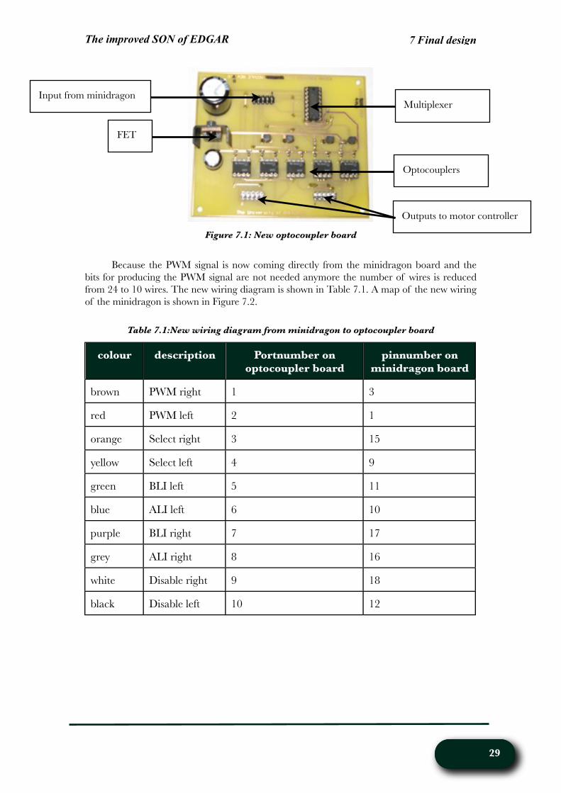
Figure 7.1: New optocoupler board
Because the PWM signal is now coming directly from the minidragon board and the bits for producing the PWM signal are not needed anymore the number of wires is reduced from 24 to 10 wires. The new wiring diagram is shown in Table 7.1. A map of the new wiring of the minidragon is shown in Figure 7.2.
Table 7.1:New wiring diagram from minidragon to optocoupler board
colour description Portnumber on optocoupler board
pinnumber on minidragon board
brown PWM right 1 3
red PWM left 2 1
orange Select right 3 15
yellow Select left 4 9
green BLI left 5 11
blue ALI left 6 10
purple BLI right 7 17
grey ALI right 8 16
white Disable right 9 18
black Disable left 10 12
The improved SON of EDGAR
2929
7 Final design
Multiplexer
Optocouplers
FET
Outputs to motor controller
Input from minidragon

Figure 7.2: New wiring map of the minidragon board
To drive the SON of EDGAR a new SIMULINK model was needed. Because the PWM signal is now generated by the minidragon board the PWM signal has not to be divided into bits any more. The PWM signal is directly send to the motor controller. The new model is shown in Appendix K.
The output from the minidragon to the motorcontroller and to the taillights used the same PWM signal generator. Because there was some noise in the signal from the steering potentiometer, this influenced the PWM signal and caused some jittering when driving at a low speed. Also the PWM frequencies of the brakelights (1000Hz), indicators(1Hz) and the motorcontroller (10000Hz) were different.
To overcome the problems with the jittering two things were done. Thirst the indicator output was changes from a PWM output to a digital output. The second one was made by changing the PWM frequency from the motorcontroller and the brakelights both to 5000Hz.
Now there is just one PWM frequency generated and there is no more noise of the steering potentiometer affecting the signal send to the motorcontroller. Table 7.2 shows the new pin numbers for the taillights.
The improved SON of EDGAR
30
7 Final design

Table 7.2: New pin numbers for the taillights
description pin number
Indicator left 94
Indicator right 93
Brakelight left 111
Brakelight right 109
The improved SON of EDGAR
3131
7 Final design
8 Conclusion
The aim of this traineeship was to improve the SON of EDGAR, especially the electronics of the scooter, as well to provide a clear documentation of the changes made and improvements implemented. The purpose of the detailed documentation was to make it easier for future work to continue with the SON of EDGAR.
In order to improve the SON of EDGAR a literature study was done to become familiar with the electronic circuit boards on the SON of EDGAR. With this knowledge it was possible to redesign the electronics and improve it compared with the old electronics.
With the new electronics it was possible to increase the ability to ride and to decrease the chance of risk due to electronic failure. With the new lay-out of the electronics it is considerably easier to understand what happens inside the SON of EDGAR.
The work that was done during this traineeship provides a good foundation to build on in the future. Because of the results of this traineeship it should be possible to add some other improvements in a short amount of time.
Reflecting on the time spent during this traineeship, a lot of effort and energy was spent in becoming familiar with electronic design. The results of this can be seen in a lot neater and clearer electronic lay-out.
Also the link between software and electronics is made much clearer during this traineeship, with the SIMULINK model modified for clarity and all blocks and signals labelled properly.
The improved SON of EDGAR
32
8 Conclusion

9 Recommendations
Despite all the effort and time put in this project there is still some work that can be done in the future to improve the SON of EDGAR further. Some of this work is discussed in the following sections and some recommendations are made.
9.1 Backlash free gearbox
To improve the comfort of riding on the SON of EDGAR, especially when standing upright, it is recommended to use backlash free gearboxes. The gearbox that is currently used in the SON of EDGAR suffers under the usage of it and the backlash is getting worse.
Due to the backlash in the gearbox, when the direction of travel is changed the gears come lose from each other for a short period, when the gears are contact again this causes an impulse resulting in a jerk of the scooter.
9.2 Enabled encoders for closed loop feedback
The second recommendation is to enable the encoders. The encoders are already implemented in the motors but they are not connected with the minidragon. The reason is that with the frequency of 100Hz the resolution of the angle measurement is too small. If the scooter drives at 17 km/h the resolution would become as follows:
€
170003600
= 4.72m /s
0.508 ⋅ π =1.596m (circumference wheel)4.72
1.596= 2.959rotations /s
2.959100
⋅ 2π = 0.18rad /measurement
0.18 ⋅ 3602π
=10.7deg rees /measurement
To make this resolution smaller a separate board is needed that processes the data from the encoders.
9.3 Proper system identification
If the encoders are enabled a proper system identification can be done. If all the characteristics of the SON of EDGAR are analysed a better model can be made and state space control can be implemented to improve the stability and drivability furthermore.
9.4 Adding a gyroscope in the yaw plane
At the moment the steering of the SON of EDGAR is don with a potentiometer. But by adding a gyroscope in the yaw plane (perpendicular with the other gyroscope) it should be possible to steer by leaning to the left and the right.
The improved SON of EDGAR
3333
9 Recommendations

References
Amerongen, J. van, Vries, T.J.A. de, 2003, Digital Control Engineering, University of Twente, Enschede
Baker, N.P, Brown, C.P., Dowling, D.R.S, Modra, J.L, Tootell, D.J 2006, SON of EDGAR State-SPace Control of Electro-Drive Gravity-Aware Ride, Adelaide
Cazzolato, B 2006, Advanced Automatic Control, University of Adelaide, Adelaide
Dijk, J van 2005, Systeem- en Regeltechniek, University of Twente, Enschede
dSPACE Inc. 2006, ControlDesk 2.3, (Release 3.5), computer program, dSPACE Inc., Novi, MI, USA
Franklin, G.F, Powell, J.D, Emami-Naeini, A. 2002, Feedback Control of Dynamic Systems, Pearson, USA
Jaycar Electronics 2006, Jaycar Engineering Catalogue, Australia
MathWorks 2006, Matlab, ver. 6.5, computer program, MathWorks Inc., Natick, MA, USA
MathWorks 2006, Matlab, ver. 7, computer program, MathWorks Inc., Natick, MA, USA
Wornle, F, 2006, RTMC9S12-Target A SIMULINK target for real-time control using Freescale MC9S12DP256 microcontrollers, University of Adelaide, Adelaide
Altium Designer, ver. 6, computer program,Altium Limited, Sydney, Australia
The improved SON of EDGAR
34
References

A. Appendix
A. Experiments
In order to familiarise myself with practical PID tuning (such as the Ziegler Nichols method) and the issues face with real hardware experiments were undertaken on several rigs designed for undergraduate control labs.
A.1 Fan Plate
The first experiment is the fan/plate rig (Figure A.1). A brushed DC motor is used to drive a fan. The air from the fan blows against the plate, thereby adjusting the angle of the plate. A potentiometer is used to measure the plate angle. The task is to drive the motor in order to control the plate angle. The hardware elements of the fan plate configuration includes:
• Fan• Plate• Potentiometer (sensor to measure the angle)• DS1104 Control Desk• Computer• Protractor (to measure the angle manually)
The position of the fan can be adjusted horizontally to affect the plant gain time delay.
Figure A.1: Fan/plate rig
To design a controller for this rig the Chien, Hrones & Reswick (C,H&R) method is used. This method is related to the Ziegler and Nichols (Z&N) method. In this method the controller parameters are designed in such a way that after 1 period the response is reduced with a decay ratio of 0.25. The decay ratio of 0.25 corresponds with a ζ=0.21, which is a good compromise between a quick response and still being stable. The difference between the Z&N method and the C,H&R method is that the latter gives a better closed loop response. The C,H & R method provides a choice of two different performance options. The first one for the quickest response without overshoot, the second one is the quickest response with a 20% overshoot. For this experiment the quickest response without overshoot is used.
Two parameters for the controller are a function of a and L. These two parameters come directly from the open loop step response plot. In this plot a straight best-fit line is drawn by the step response of the system. With this line the two parameters can be determined, as shown in Figure A.2 these parameters are:
The improved SON of EDGAR
3535
A Experiments

a=8,6L=0,33
a=8,6
L=0,33
Figure A.2: Open loop step response of fan/plate
With these parameters the control gains of a PID controller can be calculated. For a PID controller with no overshoot, the following regulator parameters are suggested.
K (Proportional Term) Ti (Integral Term) Td (Derivative Term)PID 0.95/a 2.4L 0.42L
Instead of using the Integral and Derivative Terms, the gains are used. These can be calculated with:
€
Kp = KKi = K /TiKd = K ⋅Td
Now the controller gains for the PID controller can be calculated.
€
Kp = 8,17 V /DegreeKi = K /Ti =10,34 V/Degree/sKd = K ⋅Td = 6,13 V.s/Degree
The improved SON of EDGAR
36
A Experiments

The model of the control system for this fan/plate system was made in Simulink and is shown in Figure A.3. The sub model of the fan/plate is shown in Figure A.4. Because of high frequency noise a low pass filter was used. The pole of the filter was put at 10 Hz, it was found out this gave reasonable results. It provided a balance between filtering out noise from the pot avoiding unnecessary phase lag. So the transfer function of the low pass filter becomes:
€
Tlpf =1
12π ⋅10
s+1
The low pass filter is put behind the sensor to filter out high frequency measurement noise.
Because of a bias in the potentiometer, a constant of 2.63 V is subtracted. Also a scaling factor is used of 180/5 degrees/volts for an output in degrees.
Figure A.3: SIMULINK model of control system of fan/plate
Figure A4 illustrates the SIMULINK block called Fan/plate system
Figure A.4: Fan/plate system
The improved SON of EDGAR
3737
A Experiments
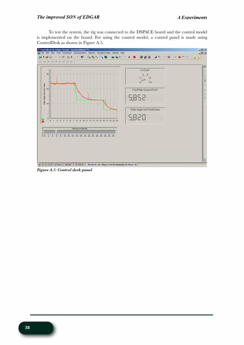
To test the system, the rig was connected to the DSPACE board and the control model is implemented on the board. For using the control model, a control panel is made using ControlDesk as shown in Figure A.5.
Figure A.5: Control desk panel
The improved SON of EDGAR
38
A Experiments

The results of the tests are shown in the Figure A.6 to Figure A.8. In the first figure there is obviously some noise. For this reason the low pass filter was used. The settling time to go from 0 degrees to 40 degrees (Figure A.8) was approximately 9 seconds.
Figure A.6: Closed loop step response of the fan/plate with PID controller
The improved SON of EDGAR
3939
A Experiments
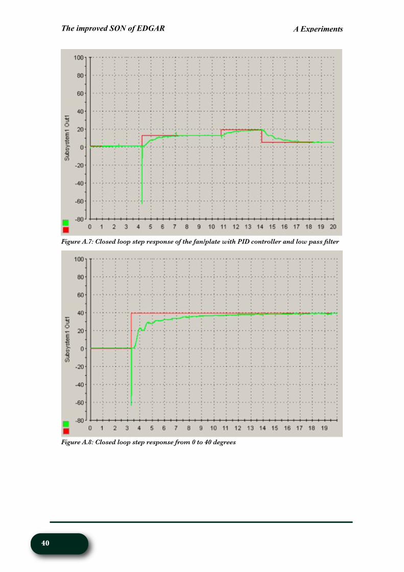
Figure A.7: Closed loop step response of the fan/plate with PID controller and low pass filter
Figure A.8: Closed loop step response from 0 to 40 degrees
The improved SON of EDGAR
40
A Experiments

A.2 Floating ping pong ball
The second experiment is a floating ping pong ball (Figure A.9). A brushed DC motor is used to drive a fan inducing a flow in the duct. The flow rate imparts a force on the ping pong ball. The objective is to adjust the fan speed to regulate the height of the ball. The hardware of the rig exists of:
• Tube• Ping pong ball• Ultrasonic sensor (for measuring the height)• Fan • DS1104 Control Desk• Computer
Figure A.9: Floating ping pong ball rig
Before starting with the real experiment, the sensor had to be calibrated. First the fan was turned off so the ping pong ball was at its lowest point. At this point the sensor gave a voltage of 0,956V. So to compensate this bias an offset was given in the SIMULINK model. When the ping pong ball was at its highest point the sensor gave a value of 4,43V. With the known height of 1,25m the sensitivity of he sensor could be calculated.
€
Sensitivity =1,25 − 0
4,43− 0,956= 0,3598m /V
This sensitivity was also brought into the SIMULINK model as a gain. Now the sensor was calibrated the open loop step response could be determined.
As in the previous experiment, also here is made use of the C,H&R method with a 0% overshoot to design a PID controller. In this case the a and the L are (Figure A.10):a=1,2L=0,8
The improved SON of EDGAR
4141
A Experiments

a=1.2
L=0.8
Figure A.10: Open loop step response ping pong ball
With these parameters the controller gains can be determined.
€
Kp =1,14Ki = K /Ti = 0,59Kd = K ⋅Td = 0,383
The gain parameters are used to make the PID controller in the Simulink model of the control system as shown in Figure A.11. The subsystem of the sensor and fan is shown in Figure A.12.
The improved SON of EDGAR
42
A Experiments

Figure A.11: Model of the control system of the ping pong ball rig
Figure A.12: Subsystem: model of the ping pong ball rig
To test the system, the rig was connected to the DSPACE board and the control model was implemented on the board. To use the control model, a control panel is made using ControlDesk as shown in Figure A.13
The improved SON of EDGAR
4343
A Experiments

Figure A.13: Controldesk lay-out ping pong ball rig
The step response of the closed loop system, with a PID controller determined with the C,R&H method, is shown in Figure A.14. It is clear that the proportional gain is too high. Even when the height is set to 0m the ping pong ball is still floating at its highest level.
The improved SON of EDGAR
44
A Experiments
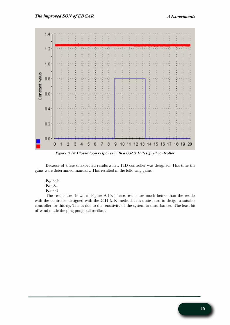
Figure A.14: Closed loop response with a C,R & H designed controller
Because of these unexpected results a new PID controller was designed. This time the gains were determined manually. This resulted in the following gains.
Kp=0,4Ki=0,1Kd=0,1The results are shown in Figure A.15. These results are much better than the results
with the controller designed with the C,H & R method. It is quite hard to design a suitable controller for this rig. This is due to the sensitivity of the system to disturbances. The least bit of wind made the ping pong ball oscillate.
The improved SON of EDGAR
4545
A Experiments

Figure A.15: Closed loop step response of the ping pong ball
The improved SON of EDGAR
46
A Experiments
B. Drawings of new handle bar stem
The improved SON of EDGAR
4747
B drawings of the new handle bar stem
The improved SON of EDGAR
48
B drawings of the new handle bar stem

The improved SON of EDGAR
4949
B drawings of the new handle bar stem
The improved SON of EDGAR
50
B drawings of the new handle bar stem

C. Features minidragon
HCS12: MiniDRAGON+ Development Board
MiniDRAGON+ features:
• RJ11 handset jack and 6-foot light weight RS232 cable for connecting the 1st SCI to a PC com port
• 110V AC adapter to power the board (US and Canada orders only)
• CD with example programs in source code
• 16 MHz crystal, 8 MHz default bus speed and up to 25MHz bus speed via PLL
• LED operating mode indication (E,J,P,B) on the 7-segment display during power-up, no need to remember jumper setting
• 3 digit diagnostic code on the 7-segment LED during power up to aid troubleshooting
• On-board BDM-in connector to be connected with a BDM from multiple venders for debugging
• On-board BDM-out connector with a 6-in BDM cable (included in price) to convert this board into a 9S12 BDM or a 9S12 programmer. No extra hardware needed.
• CAN controller, RS485 and RS232 interface chips are surface mounted on the solder side of PCB
• 7-segment LED display
• A 2-position DIP switch equivalent jumper for auto-starting four different user application programs in the 256K flash memory
• 2 pushbutton switches
• 38KHz IR receiver
• Speaker for alarm and music applications
• Potentiometer trimmer pot for analog input
• Reset and program abort buttons
• Low Voltage Inhibit reset circuit
• Small prototyping wire wrap area
• 912DP256 MCU includes the following onchip peripherals:
o 3 SPIs
The improved SON of EDGAR
5151
C Features minidragon

o 2 SCIs
o 3 CANs
o I2C interface
o 8 16-bit timers
o 8 PWMs
o 16-channel 10-bit A/D converter
• All MC9S12DP256 pins are accessible on four header connectors and different header configurations available. The header connectors can be male or female, and can be placed on the top or the bottom of PCB
• 112 Pins, up to 89 I/O-Pins
• Header connector of 2nd SCI for user's application
• 5V 1A low dropout voltage regulator, heavy duty TO220 package
• DC jack for AC adapter or DC header connector for battery in robot application
• 112 pin male headers or female receptacles for all MCU pins
• User Programmable Header for customizing your own interface to your external circuits
• Compatible with Motorola EVB9S12DP256 board
• Like Motorola EVB, supports C and Assembly language source level debugging under Code Warrior
• Can support any C compilers and Debuggers
• Program in C, BASIC, Forth and Assembly language
• Single chip mode and expanded mode
• Four operating modes: EVB, Jump-to-EEPROM, POD and Boot loader
• Header connectors for RS485 interface and CAN controller
• Many fully debugged, fairly complex 68HC12 program examples including source code, not just a "Hello World" type simple program
• Includes a test program that reads 4 switches to show their functions on the LED display while playing a song, it shows a number counting-up or counting-down, counting fast or counting slow on the 7-segment LED display, and also allows to change 7-segment LED brightness by adjusting the trimmer pot at the same time
• Super low cost and high performance
• Super fast, bus speed up to 25 MHz
• Small PC board size 2.2" X 3.2" fits into a small robot.
They look like high quality boards and each of them has own unique features, but our board will give you another choice if your budget is small. All three boards have the same MCU, the same 16 MHz crystal, basically the same hardware circuits and use the same Motorola's D-bug12 monitor, so all software can run on these boards with the same results. Whoever has a more efficient way to manufacture the board will be able to offer a better price. Fortunately Wytec has been in business since 1987 and we can produce the board at the lowest cost possible.
For a commodity product to survive, our cost is very important, but it does not mean we will sacrifice the quality. Our mission is to make quality products at low cost and the quality is still
The improved SON of EDGAR
52
C Features minidragon

our number one concern. For instance, on this board design, there are two components that we did not compromise for low cost.
1. The regular RS232 DB9 cable is too bulky and too stiff for our 68HC12 MiniDRAGON+TM. You move the DB9 cable a little bit, it moves your whole prototype chaotically. When debugging your robot application, a light weight cable can be moved by your little robot, but the regular DB9 cable can't. We pay more for a 6-foot light weight cable. Only with the light weight RS232 cable, our board can be considered as a true compact development board.
2. You can easily make a 10-pin ribbon cable for the BDM cable, because you can find a 10-pin IDC connector everywhere from Digi-Key to Mouser Electronics, but not a 6-pin IDC connector. We prefer a 6-pin ribbon cable which costs more, but it does make the product more compact..
The improved SON of EDGAR
5353
C Features minidragon

D. Map of minidragon board with port and pin numbers
The improved SON of EDGAR
54
D Map of minidragon board with port and pin numbers

E. Electronic diagrams
!!
""
##
$$
%%
&&
''
((
)*+,-
./01-2
3-4*5*67
8*9-
($
%:+-;
#<=<#="<<>
8?--+@@@@6A
B*,-;
&;C%6D/0-7+5@:7E@8-++*7F5CGGCH(IJ<!G8D?%6D%2:K7@'L;
)(MH@HMNO)@(.%@M.%M&()P3@(88QI'HR
!G<
!!
J@8D?0*E+@S@'-77*T
!U
3!
!U
3"
!U
3#
!U
3$
HQ%!
3Q%
HQ%"
3Q%
HQ%#
3Q%
HQ%$
3Q%
HQ%V
3Q%
HQ%W
3Q%
HQ%>
3Q%
HQ%X
3Q%
HQ%Y
3Q%
HQ%!<
3Q%
HQ%!!
3Q%
HQ%!"
3Q%
HQ%!#
3Q%
HQ%!$
3Q%
HQ%!V
3Q%
HQ%!W
3Q%
HQ%!>
3Q%
HQ%!X
3Q%
HQ%!Y
3Q%
HQ%"<
3Q%
HQ%"!
3Q%
HQ%""
3Q%
HQ%"#
3Q%
HQ%"$
3Q%
HQ%"V
3Q%
HQ%"W
3Q%
! " #
&P.!
O-:E-2@#
Z"$[
3Q%
RQHHP\
HQ%">
3Q%
Z"$[
3Q%
HQ%"X
RQHHP\
HQ%"Y
RQHHP\
HQ%#<
RQHHP\
HQ%#!
RQHHP\
HQ%#"
RQHHP\
HQ%##
RQHHP\
HQ%#$
RQHHP\
HQ%#V
RQHHP\
HQ%#W
RQHHP\
RQHHP\
The improved SON of EDGAR
55
E Electronic diagrams
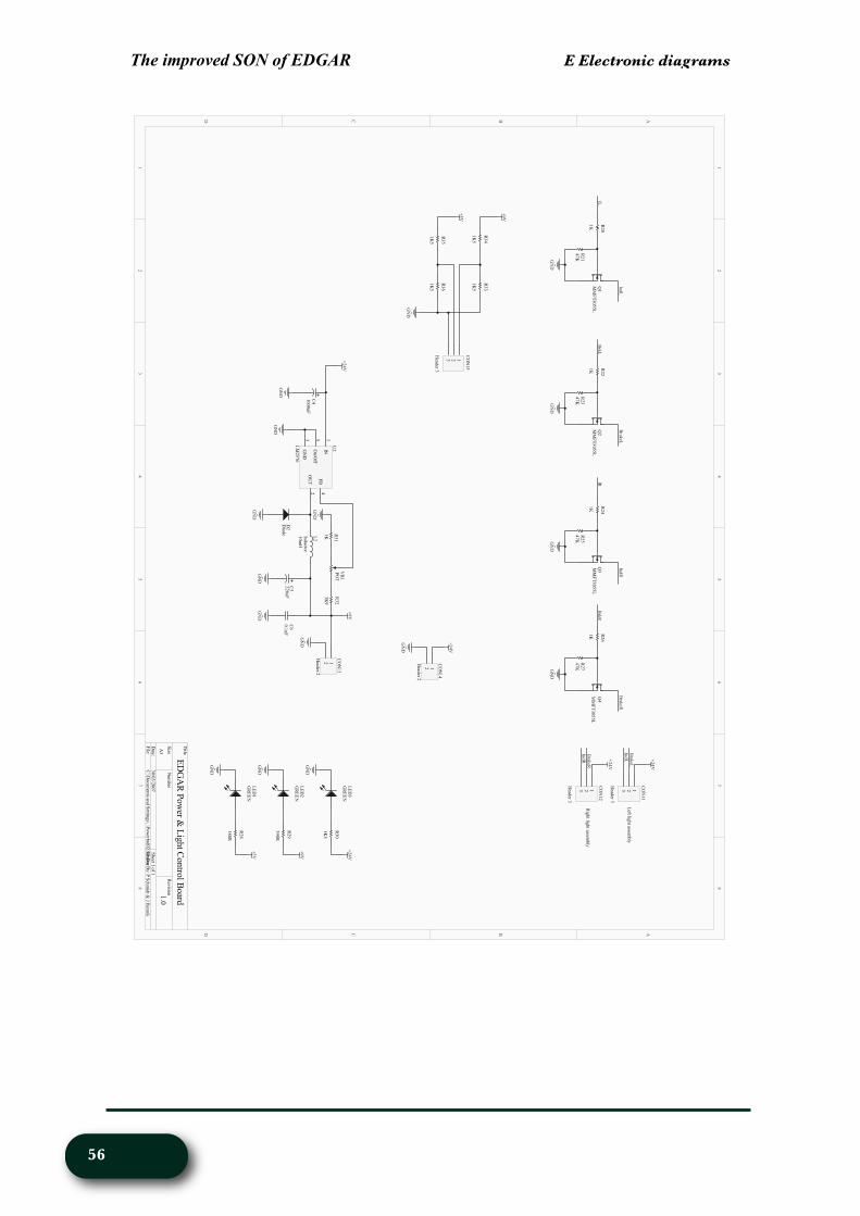
! !
" "
# #
$ $
% %
& &
' '
( (
))
**
++
,,
-./01
234516
718.9.:
;<.=1
,#
)>/1?
#@A@#A"@@'
<B11/CCCC:
DE.01?
*?F):G341;/9C>;
HC<1//.;
I9FJJFK
:L1656H@"J<GB):G
)6>L;C+M?
!N
7"@
$'N
7"!O2)
!N
7""
$'N
7"#O2)
!N
7"$
$'N
7"%O2)
!N
7"&
$'N
7"'O2)
!"#
*P2!!
Q1>H16C#
!"#
*P2!"
Q1>H16C#
R"$S
R"$S
+6>T1U
V;HU
V;H7
+6>T17
+6>T17
+6>T1U
V;H7
V;HU
U1D/C0.I
B/C>9914
50M
7.IB/C0.I
B/C>9914
50M
KC<GB4.H/CWCXC+1;;.T
!!
!J@
Y)O,7CK:L16CW
CU.IB/C*:;/6:0C+:>6H
+6TU
+6T7
V7VU
!@4Q
U"
V;H3G/:6
!@@@3E
*$
""@3E
*%
@J!3E
*&
V2!
P;APDD
%
O2)
#PZ-
"
E+
$
Z"
U["%'&
S7!
KP-
#N\
7#"
!N
7#!
O2)
O2)
)").:H1
O2)
O2)
O2)
R"$S
UY)"
O7YY2
#\@7
7"\
O2)
R\S
UY)#
O7YY2
!N%
7#@
O2)
R"$S
UY)!
O7YY2
!(@7
7"(
O2)
R%S
O2)
!"
*P2!#
Q1>H16C"
O2)
R\S
!"
*P2!$
Q1>H16C"
O2)
R"$S
!N%
7#$
!N%
7#%
!N%
7##
!N%
7#&
R\S
R%S
O2)
!"#
*P2!%
Q1>H16C#
]![[E-#@%%U
]"[[E-#@%%U
]#[[E-#@%%U
]$
[[E-#@%%U
The improved SON of EDGAR
56
E Electronic diagrams

!!
""
##
$$
%%
&&
''
((
))
**
++
,,
-./01
234516
718.9.:;
<.=1
,#
)>/1?
#@A@#A"@@'
<B11/CCCC:D
E.01?
*?F):G341;/9C>;HC<1//.;I9FJJF).9/56H@!J<GB):G
)6>K;C+L?
M2!
!
M2"
"
M2#
#
M2$
$
M2%
%
M2&
&
M2'
'
M2(
(
NO-!
!(
NO-#
!&
NO-$
!%
NO-%
!$
NO-&
!#
NO-'
!"
NO-(
!!
NO-"
!'
*NPC)
!@
Q2)
R
O!
OS2"(@#,
ST)"
ST)$
ST)&
ST)(
Q2)
ST)!
ST)#
ST)%
ST)'
#R@
7R
#R@
7!@
#R@
7!!
#R@
7!"
#R@
7!#
#R@
7!$
#R@
7!%
#R@
7!&
!"
#$
%&
'(
R!@
*N2#
U1>H16C%V"
ST)"
ST)$
ST)&
ST)(
W%X
W%X
!"
#$
%&
'(
R!@
*N2"
U1>H16C%V"
ST)!
ST)#
ST)%
ST)'
Q2)
!Y
7!
!Y
7"
!Y
7#
!Y
7$
!Y
7%
!Y
7'
!Y
7&
!Y
7(
! " #
*N2$
U1>H16C#
Q2)
W%X
ZN-!
</116.;ICZ:/CM;[3/
! " #
*N2%
U1>H16C#
! " #
*N2&
U1>H16C#
! " # $
*N2'
U1>H16C$
! " # $ %
*N2R
U1>H16C%
Q2)
Q2)
$Y'
7!(
$Y'
7!'
Z6:\S
Z6:\7
Q2)
W%X
T;GS!
T;GS"
! " # $
*N2(
U1>H16C$
Q2)
W%X
T;G7!
T;G7"
Q2)
W%X
,GG0
XGG
!
Q2)
"
7,-T
#
"X%
$
-TPZ
%
<-"
&
<-!
'
Q]7N!
,)V7<#@@
Q2)
W%X
!Y
7!R
QL6:
WX.;
!
^X.;
"
WX:3/
#
2*
$
^X:3/
%
)*)*!
<S_@%,^@%
)!
).:H1
!@@@3E
*!
! "
*N2!
U1>H16C"
E!%,
Q2)
Q2)
!@@@3E
*#
!@@[E
*"
$'4U
S!
Q2)
Q2)
Q2)
W%X
T)Q,7C).9/6.53/.:;C+:>6H
!
!J@
!ZC<GB4.H/C`CaC+1;;.b
Q2)
Z6:\S
Z6:\7
T;GS!
T;GS"
T;G7!
T;G7"
,GG0
QL6:
ZN-!
W"$X
!"
#$
%&
'(
R!@
!!!"
!#!$
!%!&
*N2!@
U1>H16C(V"
M7MS+6bS
+6b7
Q2)
W"$X
W!(X
W!(X
##@7
7#'
)#!2$'$&,
Q2)
W!(X
W%X
W%X
The improved SON of EDGAR
57
E Electronic diagrams

! !
" "
# #
$ $
%%
&&
''
((
)*+,-
./01-2
3-4*5*67
8*9-
($
%:+-;
#<=$<"==>
8?--+@@@@6
AB*,-;
&;C%6D/0-7+5@:7
E@8-++*7
F5CGGCH
:*7I6J-2=!G8D?%6D
%2:J7@'K;
L%M(3@I6J-2@%
*5+2*1/+*67@&*2D/*+3LN@!G=
!!
I@8D?0*E+@@O@'
-77*P
':++-2K@!!"N@"=(?
':++-2K@"
!"N@"=(?
&'!
&*2D/*+@'2-:P
-2@>=(
B!
B/5-@$=(
B"
B/5-@$=(
)!!
)""
)##
)$$
)RR
)>>
)-20*7:,@'
:2@!S>3)!
!
)""
)##
)$$
)RR
)>>
)-20*7:,@'
:2@"S>
!"H6+62@S-A+
!"H6+62@3*F?+
!"I6J-2@T
@&67+26,@16:2E
!"
&?:2F-2@U7
V/+
The improved SON of EDGAR
58
E Electronic diagrams
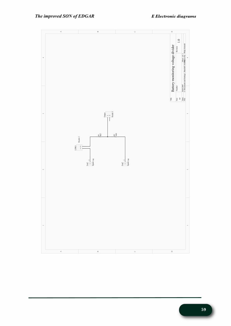
!!
""
##
$$
%%
&&
''
((
)*+,-
./01-2
3-4*5*67
8*9-
($
%:+-;
#<=<#="<<>
8?--+@@@@6A
B*,-;
&;C%6D/0-7+5@:7E@8-++*7F5CGGC':+D?H<!G8D?%6D
%2:I7@'J;
!!
K/F!
8L:E-@K/F
!!
K/F"
8L:E-@K/F
$M>
3!
!"
KN.M!
O-:E-2@"
! "
P/+L/+
O-:E-2@"
!!
!G<
':++-2J@067*+62*7F@46,+:F-@E*4*E-2
Q?*,*L@8D?0*E+
!M<
3"
The improved SON of EDGAR
59
E Electronic diagrams

! !
" "
# #
$ $
% %
& &
' '
( (
))
**
++
,,
-./01
234516
718.9.:
;<.=1
,#
)>/1?
!!@A$@"AA'
<B11/CCCC:
DE.01?
*?F):G341;/9C>;
HC<1//.;
I9FJJFK
LMA#J<GB):G
)6>N;C+O?
KLMCM:/:6C*:;/6:0016CPCQ
)R,7CK6:S1G/
#JA
!!KB.0.TC<GB4.H/
7191/
!
K)A
"
K)!
#
U-,VC"
$
U-,VC!
%
K)"
&
K)#
'
K)$
(
K)%
W
R2)
!A
K)&
!!
K+A
!"
K+!
!#
K+"
!$
K+#
!%
K+$
!&
K+%
!'
K+&
!(
K+'
!W
X**
"A
Y"-Z2["#!#
R2)
\%X
! "
U!$M]= ""TE
*!!
R2)
!A^
7!
!3E
*!A
\%X
R2)
!"
#$
%&
'(
W!A
!!!"
!#!$
!%!&
*_2"
]1>H16C(U"
)>/>,
!
)>/>,
"
)>/>,
#
)>/>,
$
)>/>,
%
)>/>,
&
)>/>,
'
)>/>,
A)>/>,
!)>/>,
")>/>,
#)>/>,
$)>/>,
%)>/>,
&)>/>,
'
)>/>,
A
<101G/,
,VZ,
+VZ,
).9>5
01,
!"
#$
%&
*_2#
]1>H16C#U"
)>/>,
%)>/>,
&)>/>,
'
R2)
\%X
7<-!
7<-!
<101G/,
7191/
!
K)A
"
K)!
#
U-,VC"
$
U-,VC!
%
K)"
&
K)#
'
K)$
(
K)%
W
R2)
!A
K)&
!!
K+A
!"
K+!
!#
K+"
!$
K+#
!%
K+$
!&
K+%
!'
K+&
!(
K+'
!W
X**
"A
Y#-Z2["#!#
R2)
\%X
! "
U"$M]=
R2)
!A^
7"
!3E
*!#
\%X
R2)
!"
#$
%&
'(
W!A
!!!"
!#!$
!%!&
*_2$
]1>H16C(U"
<101G/+
,VZ+
+VZ+
).9>5
01+
!"
#$
%&
*_2%
]1>H16C#U"
)>/>+
%)>/>+
&)>/>+
'
R2)
\%X
7<-"
7<-"
<101G/+
)>/>+
A
)>/>+
!
)>/>+
"
)>/>+
#
)>/>+
$
)>/>+
%
)>/>+
&
)>/>+
'
)>/>+
A)>/>+
!)>/>+
")>/>+
#)>/>+
$)>/>+
%)>/>+
&)>/>+
'
""TE
*!"
""TE
*!$
""TE
*!%
""A7
7#
""A7
7$
\%X
_T/:,!
_T/:,!
_T/:,"
_T/:,"
_T/:+!
_T/:+"
_T/:+!
_T/:+"
,VZ,
+VZ,
).9>5
01,
).9>5
01+
,VZ+
+VZ+
""A7
7%
""A7
7&
""A7
7'
""A7
7(
""A7
7W
""A7
7!A
""A7
7!!
""A7
7!"
!"
#$
%&
'(
W!A
*_2&
]1>H16C%U"
R2)M!
\!"XM!
M!)Z<
M!,]Z
M!+]Z
M!,VZ
M!+VZ
\!"XM!
M!,]Z
M!+]Z
M!,VZ
M!+VZ
M!)Z<
R2)M!
!"
#$
%&
'(
W!A
*_2'
]1>H16C%U"
R2)M"
\!"XM"
M")Z<
M",]Z
M"+]Z
M",VZ
M"+VZ
\!"XM"
M",]Z
M"+]Z
M",VZ
M"+VZ
M")Z<
R2)M"
Z2!
#
_Y-
"
R2)
Y!V'(A%*X
R2)
R2)
R2)
R2)
)!
!2$AA$
!AAA3E
*!
""A3E
*#
AJ!3E
*"
!"
*_2!
]1>H16C"
R2)
\%X
R2)
AJ!3E
*$
AJ!3E
*%
AJ!3E
*&
AJ!3E
*'
AJ!3E
*(
AJ!3E
*W
\%X
R2)
R2)
R2)
R2)
,!
^"
^#
,$
Q%
*&
*'
Q(
Y$ZV)'$
,!
^"
^#
,$
Q%
*&
*'
Q(
Y&
ZV)'$
,!
^"
^#
,$
Q%
*&
*'
Q(
Y%
ZV)'$
,!
^"
^#
,$
Q%
*&
*'
Q(
Y'
ZV)'$
,!
^"
^#
,$
Q%
*&
*'
Q(
Y(
ZV)'$
!^7!#
!^7!$
!^7!%
!^7!&
!^7!'
!^7!(
!^7!W
!^7"A
M",]Z
M"+]Z
M",VZ
M"+VZ
R2)M"
R2)M!
M!,]Z
M!+]Z
M!,VZ
M!+VZ
The improved SON of EDGAR
60
E Electronic diagrams

F. C. code PWM controller
CRICOS Provider Code 00123M
//Author:- Philip Schmidt//For:- The University of Adelaide - Mechanial Engineering (Jan Bennik)//Date:- 21/03/2007//Filename:- ISOPWM03.c//Clock Frequency:- 4MHz
/*Description:- A new direction. This code is a completely different way of going *about things. The compare register is now loaded when the timer overflows. */
#include <tiny2313.h>
//Program defines#define select 0x04 //PWM output select pin PD2#define out1 0x08 //PWM output 1 pin PD3#define out2 0x10 //PWM output 2 pin PD4#define out12 0x18 //both PWM output pins
//interrupt function prototypesinterrupt [TIM0_OVF] void timer0_ovf_isr(void);interrupt [TIM0_COMPA] void timer0_compa_isr(void);
//Function prototypesvoid mcuset(void); //function to setup MCU
//Program variablesunsigned char PWMval = 0x00;
//Program mainvoid main(void){ mcuset(); //setup MCU #asm("sei") //enable interrupts for(;;){ PWMval = ~PINB; //get PWM data in from PORTB //PWMval &= 0xfe; //mask off bit one //check for PWM off condition and apply to required output pin if(PWMval <= 0x01){ TCCR0B = 0x00; //stop the PWM timer if(PIND & select){ //if select is high PORTD &= ~out1; //turn on Optocoupler 1 }else{ PORTD &= ~out2; //otherwise turn on optocoupler 2 } } //check for PWM flat out condition and apply to output pin if(PWMval == 0xff){ TCCR0B = 0x00; //stop the PWM timer
The improved SON of EDGAR
61
F C. code PWM controller

if(PIND & select){ //if select is high PORTD |= out1; //turn on Optocoupler 1 }else{ PORTD |= out2; //otherwise turn on optocoupler 2 } } //everthing else if((PWMval >= 0x02) && (PWMval <= 0xfe)){ TCCR0B = 0x01; //start the PWM timer OCR0A = PWMval; //load the compare register from PORTB } } }
//Function to setup MCU for applicationvoid mcuset(void){ //setup ports DDRD = 0b00011000; //make opto control pin outputs PORTD = 0b00011100; //turn on pullup for input and turn off optocouplers DDRB = 0b00000000; //make Port B all inputs PORTB = 0b11111111; //enable port B pullups
// Timer/Counter 0 initialization // Clock source: System Clock // Clock value: No prescaller // Mode: Fast PWM top=FFh // OC0A output: Disconnected // OC0B output: Disconnected TCCR0A=0x03; TCCR0B=0x02; TCNT0=0x00; OCR0A=0xff; OCR0B=0x00;
// Timer(s)/Counter(s) Interrupt(s) initialization TIMSK=0x03;}
// Timer 0 overflow interrupt service routineinterrupt [TIM0_OVF] void timer0_ovf_isr(void){ PORTD |= out12; //turn off Optocoupler 1 and 2 //OCR0A = PWMval; //load the compare register from PORTB}
// Timer 0 output compare A interrupt service routineinterrupt [TIM0_COMPA] void timer0_compa_isr(void){ if(PIND & select){ //if select is high PORTD &= ~out1; //turn on Optocoupler 1 }else{ PORTD &= ~out2; //otherwire turn on optocoupler 2 }}
The improved SON of EDGAR
62
F C. code PWM controller

G. Specifications DC DC converter
The improved SON of EDGAR
63
G Specifications DC DC converter
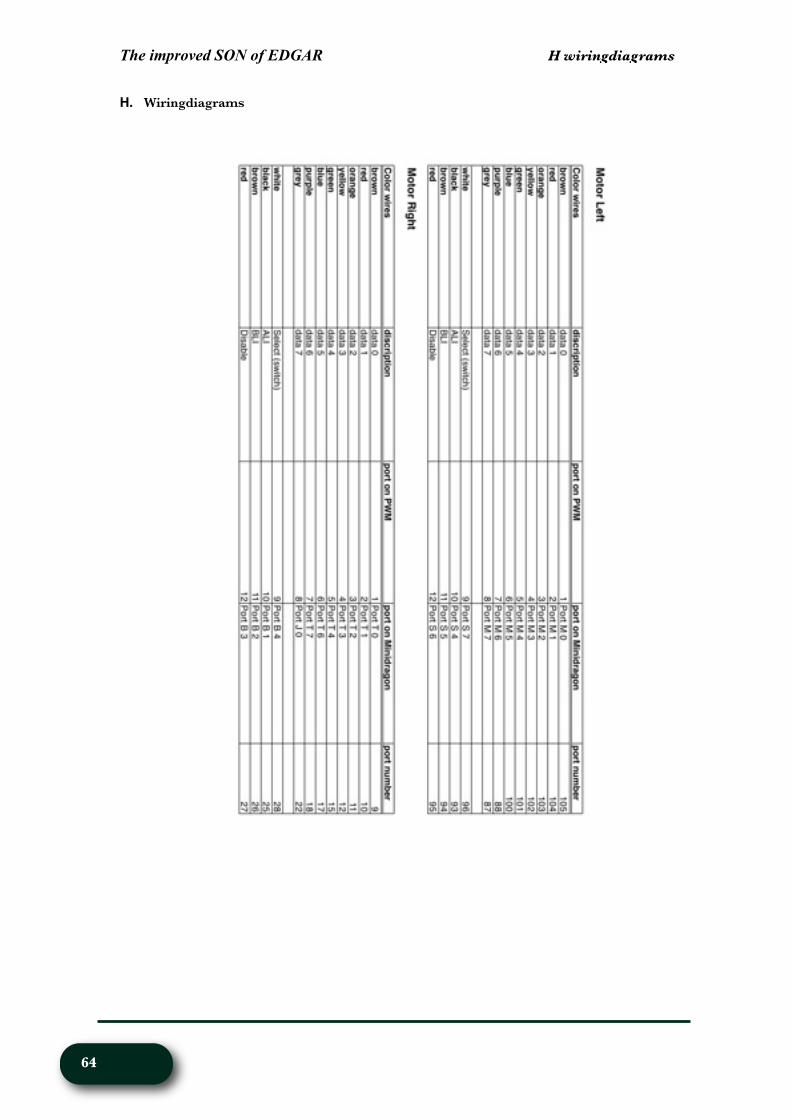
H. Wiringdiagrams
The improved SON of EDGAR
64
H wiringdiagrams

The improved SON of EDGAR
65
H wiringdiagrams

The improved SON of EDGAR
66
H wiringdiagrams
The improved SON of EDGAR
67
H wiringdiagrams

I. SIMULINK model SON of EDGAR with separate PWM controller
Vo
ltsV
olts
De
g/s
rad
/s
Vo
lts
rad
ian
s
Se
nd
in 0
-20
for a
ng
le -1
to 1
rad
Se
nd
in 0
-4 fo
r po
t
an
gle
e
rror
Vo
lts
Vo
lts
Vo
ltsra
dia
ns
Vo
ltsV
olts
Vo
ltsV
olts
rad
ian
s
-3.2
5
po
ten
tiom
ete
r bia
s v
olta
ge
Ze
ro-O
rde
rH
old
1
asin
Trig
on
om
etric
Fu
nctio
n
Su
btra
ct4
Su
btra
ct3
Su
btra
ct2
Su
btra
ct1
Su
btra
ct
In1
Rig
ht b
rea
klig
ht
Le
ft bre
aklig
ht
Su
bsyste
m2
In1
Rig
ht In
dic
ato
r
Le
ft Ind
ica
tor
Su
bsyste
m1
Ba
ttery V
olta
ge
Filte
red
Ba
ttery V
olta
ge
Ga
in
Su
bsyste
m
Sig
n
Sa
tura
tion
3
Sa
tura
tion
2
Sa
tura
tion
1
PO
RT
BP
ins: 1
,2,3
Rig
ht m
oto
r co
ntro
ller
ON
/OF
F
Vo
ltag
e
AL
I
BL
I
DIS
AB
LE
Sw
itch
RIG
HT
1
Sw
itch
du
ty in
RIG
HT
8
Qu
ad
ratic
ga
in
an
gle
(rad
)
-.15
Pro
po
rtion
al g
ain
4
.15
Pro
po
rtion
al g
ain
3
.5
Pro
po
rtion
al g
ain
2
.5
Pro
po
rtion
al g
ain
1
3
Pro
po
rtion
al g
ain
Pro
du
ct3
Pro
du
ct2
Pro
du
ct1
Pro
du
ct
1
.01
s+
1
Po
ten
tiom
ete
r low
pa
ss filte
r
AD
C In
pu
tC
ha
nn
el 6
Po
ten
tiom
ete
r
2/1
.54
Po
t Ga
in
Pu
lse
pin
: PT
P.5
Sig
n p
in: P
TP
.4P
erio
d: 1
(s)
PW
M rig
ht in
dic
ato
r
PW
M-B
, 16
-bit
Pu
lse
pin
: PT
P.3
Sig
n p
in: P
TP
.2P
erio
d: 1
e-0
05
(s)
Sa
tura
tion
: 1P
WM
righ
t bre
aklig
ht
Pu
lse
pin
: PT
P.7
Sig
n p
in: P
TP
.6P
erio
d: 1
(s)
PW
M le
ft ind
ica
tor
Pu
lse
pin
: PT
P.1
Sig
n p
in: P
TP
.0P
erio
d: 0
.00
01
(s)
PW
M le
ft bre
aklig
ht
AN
D
Lo
gic
al
Op
era
tor
PT
SP
ins: 4
,5,6
Le
ft mo
tor c
on
trolle
r
Vo
ltag
e
ON
/OF
F
Sw
itch
AL
I
BL
I
DIS
AB
LEL
EF
T1
du
ty in
Sw
itch
LE
FT
Ba
ttery V
olta
ge
LE
D1
LE
D2
LE
D3
LE
D4
LE
D5
LE
D6
LE
D7
LE
D8H
an
dle
ba
r LE
DS
AD
C In
pu
tC
ha
nn
el 4
Gyro
sco
pe
-1/.0
05
Gyro
se
nsitiv
ity2
.47
0
Gyro
bia
s @
0 ra
d/s
10
0s
10
0s +
20
s+
12
Gyro
2n
d O
rde
r (0.5
)1
PO
RT
AP
ins: 4
,5
Fo
ot s
en
so
r
PT
HP
ins: 0
,1,2
,3,4
,5,6
,7
Dig
ital o
utp
ut4
0
De
riva
tive
ga
in
s
1/6
0s+
1
De
reva
tive
pi/1
80
De
gre
es/s
ec to
rad
ian
s/s
ec
De
ad
Zo
ne
AD
C In
pu
tC
ha
nn
el 7
Ba
ttery
vo
ltag
e
Ad
d3
Ad
d
AD
C In
pu
tC
ha
nn
el 5
Acce
lero
me
ter
2.5
11
Acce
laro
me
ter b
ias 2
0 d
eg
ree
s
20
s+
1
10
0s +
20
s+
12
Acce
l 2n
d O
rde
r (0.5
)1
|u|
Ab
s1
|u|
Ab
s
The improved SON of EDGAR
68
I SIMULINK model SoE with seperate PEM controller

J. PWM to bit converter
In1
Bit1
Bit2
Bit3
Bit4
Bit5
Bit6
Bit7
Bit8
unit8 to 8bit
(double)
dc9
(double)
dc8
(double)
dc7
(double)
dc6
(double)
dc5
(double)
dc4
(double)
dc3
(double)
dc2
(double)
dc1
256
Gain
PTJPins: 0
Digital output2
PORTBPins: 4
Digital output1
PTTPins: 0,1,2,3,4,6,7
Digital output
(uint8)
Data Type Conversion
2
duty in
1
Switch
The improved SON of EDGAR
69
J PWM to bit converter

K. SIMULINK model with optocoupler
Volts
Volts
Volts
Volts
Volts
Volts
Deg/s
rad/s
Volts
radia
ns
Send in
0-2
0 fo
r angle
-1 to
1 ra
dS
end in
0-4
for p
ot
angle
erro
r
Volts
Volts
Volts
radia
ns
radia
ns
theta
Vp
VqVd
V
-3.2
5
pote
ntio
mete
r bia
s v
olta
ge
Zero
-Ord
er
Hold
1
asin
Trig
onom
etric
Functio
n
Subtra
ct2
Subtra
ct1
Subtra
ct
In1
Rig
ht b
rake lig
ht
Left b
rake lig
ht
Subsyste
m2
In1
Rig
ht In
dic
ato
r
Left In
dic
ato
r
Subsyste
m1
Batte
ry V
olta
ge
Filte
red B
atte
ry V
olta
ge
Gain
Subsyste
m
Sig
n
Satu
ratio
n3
Satu
ratio
n2
Satu
ratio
n1
-.2
Rig
ht m
oto
r ste
erin
g g
ain
.5
Rig
ht m
oto
r driv
e g
ain
PT
SP
ins: 4
Rig
ht In
dic
ato
r
9
Quadra
tic g
ain
angle
(rad)
PW
M-A
, 8-b
itP
uls
e p
in: P
TP
.1S
ign p
in: P
TT
.4P
erio
d: 0
.0002 (s
)S
atu
ratio
n: 1
Puls
e w
idth
modula
tion1
PW
M-B
, 8-b
itP
uls
e p
in: P
TP
.3S
ign p
in: P
TT
.0P
erio
d: 0
.0002 (s
)S
atu
ratio
n: 1
Puls
e w
idth
modula
tion
4.5
Pro
portio
nal g
ain
Pro
duct3
Pro
duct2
Pro
duct1
Pro
duct
1
.01s+
1
Pote
ntio
mete
r low
pass filte
r
AD
C In
put
Channel 6
Pote
ntio
mete
r
2/1
.54
Pot G
ain
PW
M-A
, 8-b
itP
uls
e p
in: P
TP
.5S
ign p
in: P
TS
.6P
erio
d: 0
.0002 (s
)S
atu
ratio
n: 1
PW
M rig
ht b
rake lig
ht1
Puls
e p
in: P
TP
.7S
ign p
in: P
TS
.7P
erio
d: 0
.0002 (s
)P
WM
left b
rake lig
ht1
AN
D
Logic
al
Opera
tor
.2
Left m
oto
r ste
erin
g g
ain
.5
Left m
oto
r driv
e g
ain
PT
TP
ins: 5
,6,7
Left m
oto
r contro
ller1
PT
TP
ins: 1
,2,3
Left m
oto
r contro
ller
PT
SP
ins: 5
Left In
dic
ato
r1
Volta
ge
ON
/OF
F
ALI
BLI
DIS
AB
LEL
EF
T2 V
olta
ge
ON
/OF
F
ALI
BLI
DIS
AB
LEL
EF
T1
Batte
ry V
olta
ge
LE
D1
LE
D2
LE
D3
LE
D4
LE
D5
LE
D6
LE
D7
LE
D8H
andle
bar L
ED
S
AD
C In
put
Channel 4
Gyro
scope
-1/.0
05
Gyro
sensitiv
ity2.4
70
Gyro
bia
s @
0 ra
d/s
100s
100s +
20s+
12
Gyro
2nd O
rder (0
.5)1
PO
RT
AP
ins: 4
,5
Foot s
ensor
PT
HP
ins: 0
,1,2
,3,4
,5,6
,7
Dig
ital o
utp
ut4
0
Deriv
ativ
e g
ain
s
1/6
0s+
1
Deriv
ativ
e
pi/1
80
Degre
es/s
ec to
radia
ns/s
ec
Dead Z
one
AD
C In
put
Channel 7
Batte
ry v
olta
ge
Add3
Add2
Add1
Add
AD
C In
put
Channel 5
Accele
rom
ete
r2.5
11
Accela
rom
ete
r bia
s 2
0 d
egre
es
20s+
1
100s +
20s+
12
Accel 2
nd O
rder (0
.5)1
The improved SON of EDGAR
70
K SIMULINK model with optocoupler


![Anextensivereviewofvibrationmodellingofrollingelementbeari ...data.mecheng.adelaide.edu.au/avc/publications/public_papers/2015/... · localisedandextendeddefects ... [170], ANSI (American](https://static.fdocuments.us/doc/165x107/5add2ae77f8b9aa5088c7ca7/anextensivereviewofvibrationmodellingofrollingelementbeari-data-170-ansi.jpg)