Reliability of Advanced Interconnect Structures - · PDF fileReliability of Advanced...
27
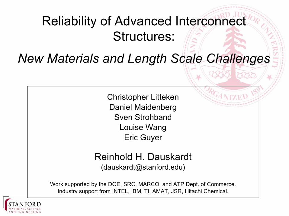
Christopher Litteken Daniel Maidenberg Sven Strohband Louise Wang Eric Guyer Reinhold H. Dauskardt ([email protected]) Work supported by the DOE, SRC, MARCO, and ATP Dept. of Commerce. Industry support from INTEL, IBM, TI, AMAT, JSR, Hitachi Chemical. Reliability of Advanced Interconnect Structures: New Materials and Length Scale Challenges
Transcript of Reliability of Advanced Interconnect Structures - · PDF fileReliability of Advanced...
Christopher LittekenDaniel Maidenberg
Sven StrohbandLouise Wang
Eric Guyer
Reinhold H. Dauskardt([email protected])
Work supported by the DOE, SRC, MARCO, and ATP Dept. of Commerce. Industry support from INTEL, IBM, TI, AMAT, JSR, Hitachi Chemical.
Reliability of Advanced Interconnect Structures:
New Materials and Length Scale Challenges
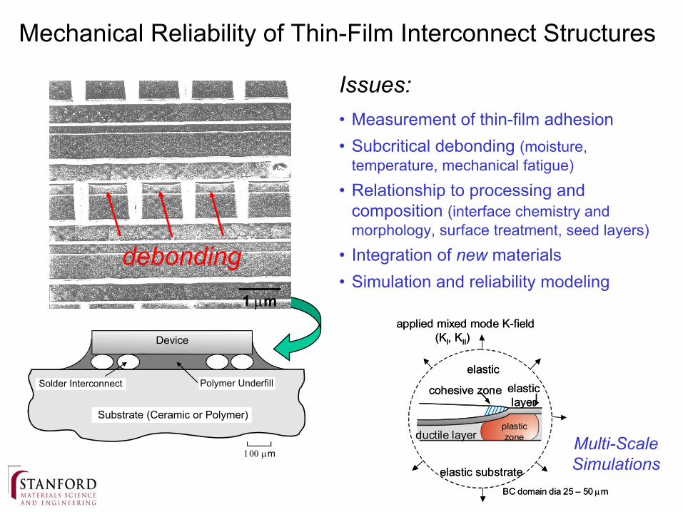
Mechanical Reliability of Thin-Film Interconnect Structures
Issues:• Measurement of thin-film adhesion• Subcritical debonding (moisture,
temperature, mechanical fatigue)
• Relationship to processing and composition (interface chemistry and morphology, surface treatment, seed layers)
• Integration of new materials• Simulation and reliability modeling
debonding
Device
Substrate (Ceramic or Polymer)
Solder Interconnect Polymer Underfill
100 µ m
applied mixed mode K-field(KI, KII)
ductile layerplasticzone
elastic
elastic substrate
cohesive zone elasticlayer
BC domain dia 25 – 50 µm
applied mixed mode K-field(KI, KII)
ductile layerplasticzone
elastic
elastic substrate
cohesive zone elasticlayer
BC domain dia 25 – 50 µm
Multi-ScaleSimulations
1 µm
Outline• Adhesion and Fracture Involving Brittle Dielectric Layers
– barriers and dielectrics in interconnect structures (TiN, TaN, SiNx, SiO2)– new low-k dielectric materials (e.g. CDO, MSSQ, SiLK, porosity)
• Moisture and Implications for CMP
– moisture assisted subcritical debonding– kinetic models and understanding
• Multi-Scale Simulations of Adhesion– interface cohesive zones and plasticity in ductile layers– barrier layer stiffness, thickness and effects of pre-stressed thin films
• Patterned Structures– elastic constraint and stress state– effect of line geometry

Interface Fracture Resistance and Reliability
Gtotal = Go + Gzone
interface chemistry
frictional contactductile adjacent layer
Plastic Zone
Fracture ProcessZone, Go
Adsorbed layer
Elastic Layer
Elastic Substrate
SurfaceRoughness, λ Ductile Layer, hD
BarrierLayer, hb
Interface Fracture Energy
Of interest….• New materials
• brittle glasses• ductile polymers• porosity (density)
• Length scales effects• mechanical properties• adhesion• 1-D, 2-D, complex
structures
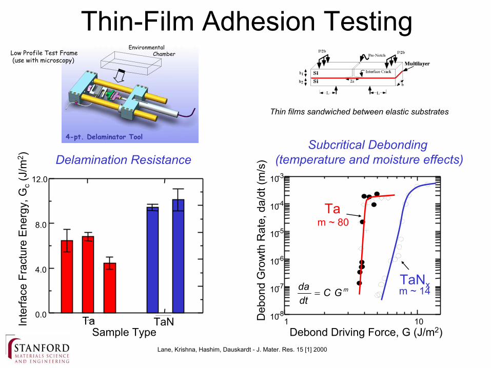
Thin-Film Adhesion Testing
Subcritical Debonding(temperature and moisture effects)
1 10Debond Driving Force, G (J/m2)
10-8
10-7
10-6
10-5
10-4
10-3
m ~ 80
m ~ 14mGCdtda
=
Deb
ond
Gro
wth
Rat
e, d
a/dt
(m/s
)
TaNx
Ta
1.00
Sample Type
0.0
4.0
8.0
12.0
Ta TaNInte
rface
Fra
ctur
e E
nerg
y, G
c(J
/m2 ) Delamination Resistance
Lane, Krishna, Hashim, Dauskardt - J. Mater. Res. 15 [1] 2000
Thin films sandwiched between elastic substrates
EnvironmentalChamberLow Profile Test Frame
(use with microscopy)
4-pt. Delaminator Tool

Research Activities in Low K MaterialsMaterial Class Feature Examples
DielectricConstant
Silica (SiO2) Silicon dioxide glass ThermalTEOS
3.9 – 4.1
Modified Silica Fluorinated silicaCarbon doped silica
CVD fluorinated silica (FSG)SiCOH
3.5< 3.0
Porous Silica Nanoporous silica AerogelZerogel
1.0 – 3.0
Inorganic Polymer Organically modifiedsilicate
Polysilesquioxanes (SSQ) 2.5 – 3.5
Porous Hybrids Phase separatedorganic/inorganic
PCL/SSQ hybrids 2.3 – 3.0
Organic Polymers Fluorinated and non-fluorinated polymers
Polyimide, parylene andpolynaphthalene familiesBenzocyclobutene (BCB)Aromatic Hydrocarbon (SiLK)Amorphous carbon films
1.8 – 3.5
2.72.62.7 – 3.5

CH3
Si
CH3O
Si
O
O
O
Si OH3C
O
Si O
SiO
Si
OCH3
CH3
Effect of Carbon Doping on Adhesion of CDO
4.61
8.5
2.412.8
3.57
5.355.57
3.2
3.8
4.5
0
1
2
3
4
5
6
7
8
9
10
0% 10% 20% 30% 40% 50% Graded
Inte
rface
Fra
ctur
e E
nerg
y G
c (J/
m2 )
Sample Set 2Sample Set 1
Si-CH3 / Si-O FTIR ratioSi
O
Si OO
O
Si
Si
OO
O
O
SiO
Si
O
O
O
OO
O
silica
carbon-doped
Cu
SiNx
SiO2
Si
SiNx
CDO 0.5 µm debond
J. Rim, F. Shi and R.H. Dauskardt - 2000

0 10 20 30 40 502.02.22.42.62.83.03.23.43.6
Die
lect
ric C
onst
ant k
(at 1
0KH
z)
Initial Content of Porogen (wt%)
0 10 20 30 40 500.8
1.0
1.2
1.4
1.6
Den
sity
(g/c
m3 )
Initial Content of Porogen (wt%)
0.0
0.5
1.0
1.5
2.0
2.5
3.0
5010 20 25 30 400
Frac
ture
Ene
rgy
(J/m
2 )
Initial Content of Porogen (wt%)
SoG Porosity Effects on Properties
L. Wang, J. Rim, and R.H. Dauskardt - 2002
fracture MSQ(Hitachi Chemical)

0 20 40 60 80 100
2.6
2.8
3.0
3.2
3.4
Die
lect
ric C
onst
ant k
(at 1
0KH
z)
NaOH Promoter Content (ppm)
0 20 40 60 80 1000.975
0.980
0.985
0.990
0.995
Den
sity
(g/c
m3 )
NaOH Promoter Content (ppm)0.0
0.5
1.0
1.5
2.0
2.5
3.0
10 25 50 75 1000
Frac
ture
Ene
rgy
(J/m
2 )
Promoter Content (ppm)
• Step 2: Condensation
• Step 1: Hydrolysis
Si(OR')3R + H2O ------ Si(OR')2ROH + HOR'
Si(OR')4 + H2O ------ Si(OR')3OH + HOR'
Si(OR')2CH3OH + Si(OR')3OH
CH3(OR')2Si-O-Si(OR')3 +H2O
NaOH
NaOH
SoG NaOH Promoter Effects on PropertiesL. Wang, J. Rim, and R.H. Dauskardt - 2002
R = CH3
CH3
Si
HO
Si
O
O
O
Si OH3C
O
Si O
SiO
Si
O
CH3CH3
H R = H
SoG Composition Effects on Fracture PropertiesFr
actu
re E
nerg
y, G
c(J
/m2 )
0
2
4
6
8
10
0 1 2 3
Si-O Bond Ratio, SiOx
CH3/H
CH3
SiO2“Rule of Mixture”
Models
Methyl Side Groups(R = CH3)
Hydrogen Side Groups(R = H)
L. Wang, J. Rim, F. Oota and R.H. Dauskardt - 2001
OSi
CH3
OSi
C6H5
OSi
C2H3
Methyl Vinyl Phenyl
increasing functional group size
0
1
2
3
4
5
0 20 40 60 80(Effective Functional Group Content) x (Size)
Frac
ture
Ene
rgy,
Gc
(J/m
2 )
MethylVinylPhenyl
Functional Group SizeConstant CH3, Varying H
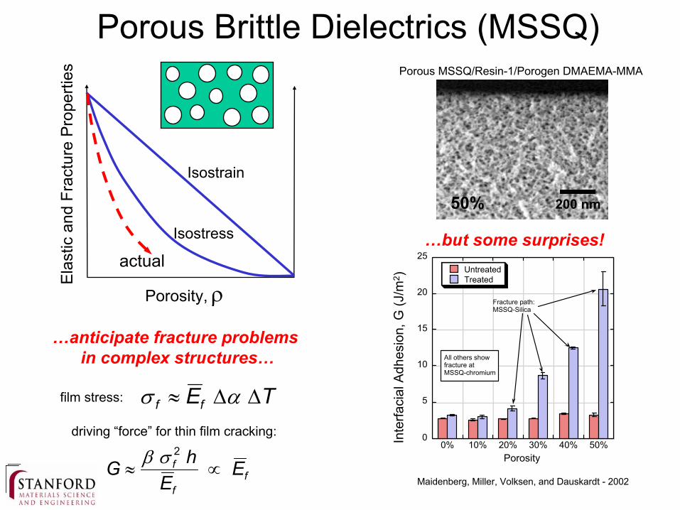
Porous Brittle Dielectrics (MSSQ)
200 nm50%
Porous MSSQ/Resin-1/Porogen DMAEMA-MMA
0
5
10
15
20
25
0% 10% 20% 30% 40% 50%
UntreatedTreated
Porosity
Fracture path:MSSQ-Silica
All others show fracture atMSSQ-chromium
Inte
rfaci
al A
dhes
ion,
G (J
/m2 )
Maidenberg, Miller, Volksen, and Dauskardt - 2002
Porosity, ρ
Ela
stic
and
Fra
ctur
e P
rope
rties
Isostrain
Isostress
actual
ff
f EE
hG ∝≈2σβ
TEff ∆∆≈ ασdriving “force” for thin film cracking:
…anticipate fracture problemsin complex structures…
film stress:
…but some surprises!
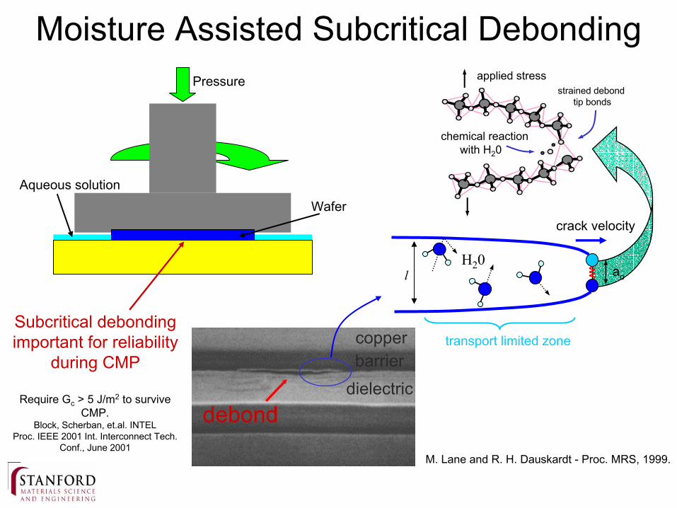
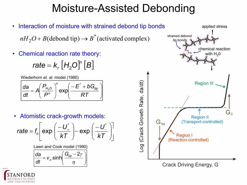
Moisture Assisted Subcritical Debonding
M. Lane and R. H. Dauskardt - Proc. MRS, 1999.
Subcritical debonding important for reliability
during CMP
strained debondtip bonds
chemical reactionwith H20
applied stress
WaferAqueous solution
Pressure
aol
crack velocity
transport limited zone
debonddielectricbarriercopper
H20
Require Gc > 5 J/m2 to survive CMP.
Block, Scherban, et.al. INTELProc. IEEE 2001 Int. Interconnect Tech.
Conf., June 2001
Crack Driving Energy, G
Region II
Region I
GC
TH
(Reaction-controlled)
(Transport-controlled)
Region III
+−
=
RTbGE
PP
Adtda tip
n
oOH
*
exp2
Moisture-Assisted Debonding
)complex activated() tipdebond( *2 BBOnH →+
[ ] [ ]BOHkrate nr 2=
strained debondtip bonds
chemical reactionwith H20
applied stress• Interaction of moisture with strained debond tip bonds
• Chemical reaction rate theory:
Wiederhorn et. al. model (1980)
• Atomistic crack-growth models:
−=
ηγ2
sinh tipo
Gv
dtda
Lawn and Cook model (1990)
−−
−= −+
kTU
kTUfrate o
**
expexp

Subcritical Delamination Behavior in Moist Environments: Temperature and Humidity Effects
−=
ηγ2sinh Gv
dtda
o
Crack-Growth Model
SiO2/TaN/Cu
debond
10Debond Driving Force, G (J/m2)
10-10
10-9
10-8
10-7
10-6
10-5
10-4
10-3
153
95% RH
50% 20%5%
T = 50oC
Del
amin
atio
n G
row
th R
ate,
da/
dt(m
/s)
10-11
10-10
10 -9
10 -8
10 -7
10 -6
10 -5
10 -4
1 10
20 at.% C
90% RH
30% RH
5 at.% C
Del
amin
atio
n G
row
th R
ate,
da/
dt(m
/s)
Debond Driving Energy, G (J/m2)
TaN/SiO2(25oC and 50% RH)
Debonding in CDO Dielectrics
threshold values crucial for reliability
M. Lane and R. H. Dauskardt - Proc. MRS, 1999.
J. Rim, F. Shi and R.H. Dauskardt - 2000

Effect of CMP Solution on Subcritical Debonding
10-10
10-9
10-8
10-7
10-6
10-5
10-4
1 2
Deb
ond
Gro
wth
Rat
e, d
a/dt
(m/s
)
Applied Strain Energy Release Rate, G (J/m2)
pH 11.0
pH 3.0
T = 30oC
Increasing pH acceleratesdelamination growth rates
E. Guyer, M. Patz and R. H. Dauskardt - 2002
Delamination observed in MSSQ
pH 3.0 solution (e.g. dielectric slurry)1.0 wt.% potassium hydrogen phthalate, hydrogen chloride 0.07 wt.%, formaldehyde 0.05 wt.%, methanol 0.02 wt.%, balance H2O
pH 11.0 solution (e.g. barrier metal slurry)0.08 wt.% Glycine, 0.03 wt.% sodium chloride, 0.02 wt.% sodium hydroxide, 0.01 wt.% disodiumethylenediaminetetraacetate anhydrous, balance H2O
Materials:JSR - LKD6103 with Poly X Cap
H2O
+− +↔ NaOHNaOH
−+ +↔ OHOHOH 3222 lone pair
orbitals1 lone pair(shields)
3 lone pairs(accelerates)
−+ +↔+ ClOHOHHCl 32
1 lone pair(shields)
3 lone pairs(accelerates)
Cra
ck G
row
th R
ate,
da/
dt(m
/s)
10-4
10-12
10-10
10-8
10-6
Stress Intensity Factor, K (MPa√m)0.3 0.4 0.5 0.6
Bulk Silica Glass(Wiederhorn – 1973)
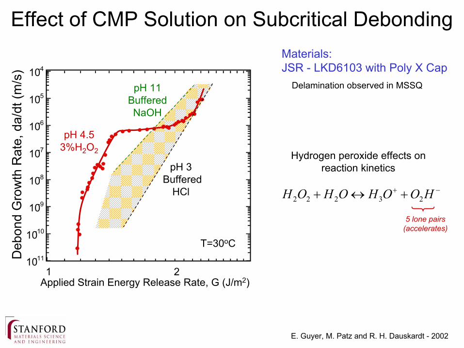
Hydrogen peroxide effects on reaction kineticspH 3
Buffered HCl
pH 11 Buffered NaOH
pH 4.5 3%H2O2
T=30oC
10-11
10-10
10-9
10-8
10-7
10-6
10-5
10-4
1 2
Deb
ond
Gro
wth
Rat
e, d
a/dt
(m/s
)
Applied Strain Energy Release Rate, G (J/m2)
E. Guyer, M. Patz and R. H. Dauskardt - 2002
−+ +↔+ HOOHOHOH 23222
5 lone pairs(accelerates)
Delamination observed in MSSQ
Materials:JSR - LKD6103 with Poly X Cap
Effect of CMP Solution on Subcritical Debonding

Debond Driving Energy, G (J/m2)1 1010 -8
10-7
10 -6
10 -5
10 -4
10 -3
Deb
ond
Gro
wth
Rat
e, d
a/dt
(m/s
)TaNx
Ta
prematurethreshold
• chemically-active species in aqueous slurries crucial for survival through CMP
Engineer interfaces immune to stress corrosion?• barrier-oxide effect on steric hindrance
Moisture and Loading Effects during CMP
ao
SiO2
TaCu
oxide
2uopH2O
SiO2
adsorbate
Competing rate effects: crack growth rate and Ta oxidization rate

Multi-Scale Simulations of 3-D Interconnect Structures
Microprocessor
n+/p+
n+/p+ n+/p+
Gate
Gate
n+/p+n+/p+
Gate
n+/p+
Reliability of Complex 3-D Structures
debond
Use simulations to predict adhesion and mechanical reliability
of more complex structuresCu
plasticzone
elastic
elastic substrate
Cohesivezone
elasticlayer
Computational Model
• finite deformation elasticity (FEM)
• large strain elastic/plastic (with hardening)
• VIB debond layer or cohesive zone
Separation, δ
Stre
ss, σ
Go ~ 5 J/m2
σmax ~ E/60
δmax
(developed from Klein and Gao - 1999)
10-2 10-1 1 100
20
40
60
80
100
20
Copper Layer Thickness, h (µm)
Inte
rface
Fra
ctur
e E
nerg
y, G
c(J
/m2 )
Dielectric layer
Si wafer
Copper layer
Barrier layer debond
2 4 6 8
250
300
350
400
450
500measured yield properties
0Copper Layer Thickness, h (µm)
Cop
per Y
ield
Stre
ss, σ
ys(M
Pa)
+
h1~ β
ασys
simulated yield properties
+h1~ β
ασys
Lane, Vainchtein, Gao, R.H. Dauskardt - J. Mater. Res. 16 [1] 2001
Cu layer thickness300 Å - 16.4 µm
Multi-Scale Simulations of Interface Fracture Resistance
Elastic barrier layer, D
Ductile copper layer, hCu

Cu metal
Ductile Organic Dielectrics: Thickness Effects on Adhesion
SiO2
CuCrSiXy
SiLK
(0.2 µm)
(0.4 µm)(0.02 µm)
(0.25 – 5.12 µm) debond
Litteken and Dauskardt - 2000
Organic Dielectric Thickness, h (µm)
Inte
rfaci
al A
dhes
ion,
Gc
(J/m
2 )
0
10
20
30
40
50
60
0.01 0.1 1 10
SiLK/SiO2
SiLK/SiO2(ozone clean)
FLARE/SiN
Yie
ld S
tress
, σys
(MP
a)
Film Thickness-1, 1/h (µm)-1
Cu
SiLK0
200
400
600
800
0 2 4 6

Technologically Relevant Values:hb ~ 5 – 100 nm
0.8 - 2.3 005 - 20066.160/
≈
≈≈≈
YS
c
YS
c
MPaGPaE
σσ
σσ
1µm Cubarrier
SiO2 dielectric
silicon
Barrier Layer Thickness Effects on Adhesion
3 4 5 6 7 8 9 10 11 12
1
2
3
4
100
50
25
10
Parameters:
H = 10 GPa
Eb
= 250 GPa
hpl
= 1.0 µm
G0
= 4 J/m2
barrier thicknesshb (nm)
5
Inte
rface
Fra
ctur
e E
nerg
y, G
ss/G
o
Normalized Cohesive Stress, σc/σys
typical values
strong interfaceweak ductile layer
weak interfacestrong ductile layer
debond
Effect of Barrier Stiffness
3 4 5 6 7 8 9 10 11 121
2
3
500
Elastic modulusEb (GPa)
125
300250200
Inte
rface
Fra
ctur
e E
nerg
y, G
ss/G
o
Normalized Cohesive Stress, σc/σys
typical values
S. Stroband and R.H. Dauskardt - 2002
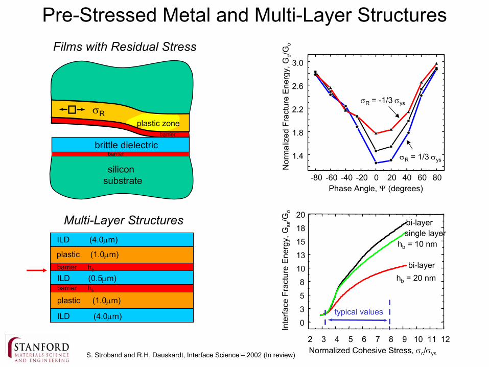
Pre-Stressed Metal and Multi-Layer Structures
silicon substrate
brittle dielectricbarrier
plastic zone
barrier
σR
S. Stroband and R.H. Dauskardt, Interface Science – 2002 (In review)
-80 -60 -40 -20 0 20 40 60 80
1.4
1.8
2.2
2.6
3.0
σR = 1/3 σys
Nor
mal
ized
Fra
ctur
e E
nerg
y, G
c/Go
Phase Angle, Ψ (degrees)
σR = -1/3 σys
2 3 4 5 6 7 8 9 10 11 12
03
58
1013151820
single layer
bi-layer
bi-layer
Inte
rface
Fra
ctur
e E
nerg
y, G
ss/G
o
Normalized Cohesive Stress, σc/σys
typical values
hb = 10 nm
hb = 20 nm
ILD (4.0µm)
ILD (0.5µm)
plastic (1.0µm)
barrier hb
plastic (1.0µm)
ILD (4.0µm)
barrier hb
Multi-Layer Structures
Films with Residual Stress
C. Litteken and Dauskardt, Int. J. Fracture – 2002 (in review)
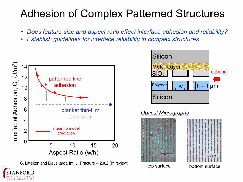
Adhesion of Complex Patterned Structures• Does feature size and aspect ratio effect interface adhesion and reliability?• Establish guidelines for interface reliability in complex structures
top surface
Optical Micrographs
bottom surface
SiliconMetal LayerSiO2
Polymer
Silicon
w h = 1 µm
debond
0
2
4
6
8
10
12
14
5 10 15 20
patterned line adhesion
Inte
rfaci
al A
dhes
ion,
Gc
(J/m
2 )
Aspect Ratio (w/h)
blanket thin-film adhesion
shear lip model prediction
400 nm 400 nm210 nm 210 nm
210 nm
210 nm
debond propagation
Cu CDO/SiLK
SiSiO2
SiC or SiN
SiC or SiN
CuTaN
690 nm
Landed Trench
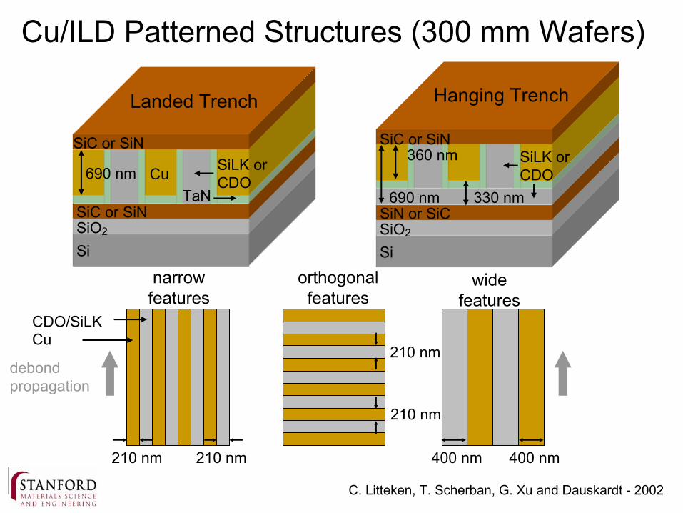
Cu/ILD Patterned Structures (300 mm Wafers)
SiSiO2
SiN or SiC
SiC or SiNSiLK or CDO
690 nm
360 nm
Hanging Trench
narrow features
orthogonal features
wide features
SiLK or CDO
330 nm
C. Litteken, T. Scherban, G. Xu and Dauskardt - 2002

0
1
2
3
4
5
6
Landed Patterned Structures –Etch Stop versus Passivation Cap Debond
pattern/passivationdebond
etch stop debond
Inte
rfaci
al A
dhes
ion,
Gc
(J/m
2 )
SiSiO2SiC
SiC
CuTaN
CDO
debonded interface
orth
ogon
al fe
atur
es
wid
e fe
atur
es
narro
w fe
atur
es

Debond Path Morphology
RMS roughness 3.8nm
RMS roughness 2.9nm
debond direction
KIKII
KIKII
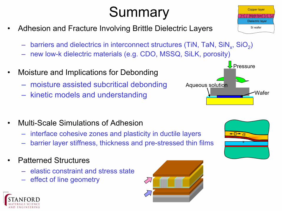
Summary• Adhesion and Fracture Involving Brittle Dielectric Layers
– barriers and dielectrics in interconnect structures (TiN, TaN, SiNx, SiO2)– new low-k dielectric materials (e.g. CDO, MSSQ, SiLK, porosity)
• Moisture and Implications for Debonding– moisture assisted subcritical debonding– kinetic models and understanding
• Multi-Scale Simulations of Adhesion– interface cohesive zones and plasticity in ductile layers– barrier layer stiffness, thickness and pre-stressed thin films
• Patterned Structures– elastic constraint and stress state– effect of line geometry
σx
Dielectric layer
Si wafer
Copper layer
Barrier layer
WaferAqueous solution
Pressure