Regulation of Output Voltage by Considering Disturbance in Source Side ... · Load Side of Single...
8
IJCTA, 8(3), 2015, pp. 1089-1096 © International Science Press Regulation of Output Voltage by Considering Disturbance in Source Side and Load Side of Single Phase Z-source Inverter (ZSI) S. Sabareswar, D. Kalyanraj and A. Stanley Jesudaiyan Abstract: This paper work aims at regulation of Z-source inverter’s (ZSI) output voltage by considering disturbance in load and source side. The ZSI unlike Current Source Inverter (CSI) and Voltage Source Inverter (VSI) has salient features such as voltage boost and buck, single stage conversion (without employing Intermediate converters) and allowing shoot through state has been discussed. The different modes of operation and output voltage equation for two modes of operation have also been discussed. The modified sinusoidal pulse width modulation technique for ZSI considering two operation modes (shoot through and non-shoot through) has been generated. Design criteria for impedance network and LC filter has been discussed. The closed loop simulation results for ZSI feeding a RL load considering disturbance in the load side and source side regulating the load voltage has been discussed. Comparison of simulation results with analytical expression has been discussed. Keywords: ZSI, control techniques, design of L and C, modified Sine PWM 1. INTRODUCTION Z-source inverter finds its use in variety of applications over a decade. Conventional inverters namely voltage source inverter and current source inverter would produce output voltage lower than or higher than the input voltage. To make these inverters to operate in both step down and step up mode extra DC converter switch is required, therefore, the control becomes complex, whereas Z-source inverter has single stage conversion of buck and boost mode by employing cross shaped LC network. In Conventional Inverters, the dead band causes distortion in the output waveform and thereby introduces harmonics [1]. In this type of inverter (ZSI), the normal mode of operation is slightly modified to act as VSI and DC-DC Boost converter. The inverter switches of the same leg are allowed to conduct at the same instant thereby shorting the source side which is prevented in case of voltage source inverter. The source side is protected with diode which prevents DC source from any damages. During this period of operation the inductor and capacitor network acts as source and boosts the power similar to DC-DC Boost converter [2],[3]. Most of the papers published over a decade discuss the control scheme for generating these pulses to converter to control load voltage subjected to disturbances in the source and load side, speed control of motor and etc. The papers based on controller design for Distributed Generation system, Uninterruptible power supplies, Motor speed control were also published and prototypes were implemented [4],[5]-[7]. This paper concentrates on inverter system by regulating the output voltage of an inverter when subjected to disturbances in source and load side pointing the advantage of single stage conversion over DC-DC Saranathan College of Engineering,Trichy-620012, Tamilnadu,India * e-mail: [email protected]
Transcript of Regulation of Output Voltage by Considering Disturbance in Source Side ... · Load Side of Single...

IJCTA, 8(3), 2015, pp. 1089-1096© International Science Press
Regulation of Output Voltage by Considering Disturbance in Source Side and Load Side of Single Phase Z-source Inverter (ZSI)S. Sabareswar, D. Kalyanraj and A. Stanley Jesudaiyan
Abstract: This paper work aims at regulation of Z-source inverter’s (ZSI) output voltage by considering disturbance in load and source side. The ZSI unlike Current Source Inverter (CSI) and Voltage Source Inverter (VSI) has salient features such as voltage boost and buck, single stage conversion (without employing Intermediate converters) and allowing shoot through state has been discussed. The different modes of operation and output voltage equation for two modes of operation have also been discussed. The modified sinusoidal pulse width modulation technique for ZSI considering two operation modes (shoot through and non-shoot through) has been generated. Design criteria for impedance network and LC filter has been discussed. The closed loop simulation results for ZSI feeding a RL load considering disturbance in the load side and source side regulating the load voltage has been discussed. Comparison of simulation results with analytical expression has been discussed.
Keywords: ZSI, control techniques, design of L and C, modified Sine PWM
1. INTRODUCTION Z-source inverter finds its use in variety of applications over a decade. Conventional inverters namely voltage source inverter and current source inverter would produce output voltage lower than or higher than the input voltage. To make these inverters to operate in both step down and step up mode extra DC converter switch is required, therefore, the control becomes complex, whereas Z-source inverter has single stage conversion of buck and boost mode by employing cross shaped LC network. In Conventional Inverters, the dead band causes distortion in the output waveform and thereby introduces harmonics [1]. In this type of inverter (ZSI), the normal mode of operation is slightly modified to act as VSI and DC-DC Boost converter. The inverter switches of the same leg are allowed to conduct at the same instant thereby shorting the source side which is prevented in case of voltage source inverter. The source side is protected with diode which prevents DC source from any damages. During this period of operation the inductor and capacitor network acts as source and boosts the power similar to DC-DC Boost converter [2],[3].
Most of the papers published over a decade discuss the control scheme for generating these pulses to converter to control load voltage subjected to disturbances in the source and load side, speed control of motor and etc. The papers based on controller design for Distributed Generation system, Uninterruptible power supplies, Motor speed control were also published and prototypes were implemented [4],[5]-[7]. This paper concentrates on inverter system by regulating the output voltage of an inverter when subjected to disturbances in source and load side pointing the advantage of single stage conversion over DC-DC
Saranathan College of Engineering,Trichy-620012, Tamilnadu,India* e-mail: [email protected]

1090
boost converter and single phase inverter system. The modes of operation, Modified Sinusoidal PWM, Design consideration of Impedance network and output filter and simulation results of all the above are presented in different sections.
Figure 1: Block diagram of single phase Impedance-source inverter with source and Load controller
2. OPERATING MODES
2.1 Non-Shoot through Mode of Operation The figure 2 shows the Voltage Source Type Single phase Z-Source Inverter (ZSI) feeding RL load.
ZSI unlike VSI and CSI has two different operating modes: (i) Non-Shoot through mode and (ii) Shoot through mode, in which the shoot through mode of operation is restricted in VSI and CSI. Since, the source will be short in both VSI as well as in CSI.
Figure 2: Voltage Source type Impedance-source inverter feeding RL load
The Load voltage (Vo) obtained in this mode of operation will be always less than input DC Voltage (Vdc). Based on the power flow, the Voltage Source type Z-source inverter is classified into three modes. They are: (i) Positive power flow (ii) negative power flow and (iii) freewheeling mode of operation. In positive power flow mode, the inverter switches S1S2 (or) S3S4 conducts and the power flow will be always from source to load. The negative power flow mode occurs when energy present in the load delivers to source via diodes. The third mode of operation freewheels within load (i.e.) either upper switches conduct or lower switches conduct. The diode will be forward biased in positive power flow mode of operation.
2.2 Shoot through mode of OperationOperating impedance source inverter in this mode differentiates from VSI as well as CSI which is shown in figure 3. In this mode, the switches of the same leg are allowed to conduct simultaneously, to regulate the load side voltage in case of disturbances in the load (or) source. In this mode the diode will be in reverse biased in order to prevent reverse flow current through the source. At any instant, three inverter switches will be conducting, sometimes all the inverter switches may conduct. Since the dc source is isolated from load, the energy is supplied by the capacitor. Under normal mode of operation, the charging of capacitor through inductor occurs and discharges during shoot through mode of operation.
S. Sabareswar, D. Kalyanraj and A. Stanley Jesudaiyan

1091
Table 1
Three switches conduct during this mode, sometimes all the switches conduct
Direction of current flow during shoot through mode of ZSI
Figure 3: Circuit diagram for Shoot through mode of ZSI
2.3 Relation between Voltage across load and Input DCVoltage of the ZSI The voltage expression of ZSI can be given as in (1)-(19)
3
lied by the capacitor. Under normal mode of operation, the charging of capacitor through inductor occurs and discharges during shoot through mode of operation.
V = V=V (1)
V=V=V (2)
where V and V are the instantaneous voltage of inductor and capacitor During non-shoot through state with time period T,the voltage equation can be given as:
V = V + V (3)
V = V − V (4)
V is the voltage across the Z-Source network By adding equations (3) and (4) we get,
V = 2V − V (5)
Similarly, for shoot through state with time period T, the voltage equation can be defined as
V = V (6)
V = 0 (7)
The inductor voltage across L& 𝐿 (V) when averaged during one switching cycle under steady state is zero.
V= 0 (8) From equations (3) and (6),we get
(V − V) T+VT= 0 (9)
where V is the capacitor voltage under steady state condition averaged over a period
Rearranging equation (9)
VT − VT+ VT = 0 (10)
VT = V (T−T) (11)
V = V T (T−T) ⁄ (12)
Using (12) in (5) we thus obtain expression for voltage across impedance-source network in terms of DC input voltage
V = 2(V T (T−T) ⁄ ) − V (13)
V = 2VT−VT + V T (T−T)⁄ (14)
V = V(T T ) (T−T)⁄ (15)
V = V T (T−T)⁄ (16)
V= B*V (17)
From the above relation obtained, the maximum value of fundamental component of Voltage across load (Vo1) is expressed in (18)
Vo1 = V * ma (18)
Regulation of Output Voltage by Considering Disturbance in Source Side and Load Side...

1092
3
lied by the capacitor. Under normal mode of operation, the charging of capacitor through inductor occurs and discharges during shoot through mode of operation.
V = V=V (1)
V=V=V (2)
where V and V are the instantaneous voltage of inductor and capacitor During non-shoot through state with time period T,the voltage equation can be given as:
V = V + V (3)
V = V − V (4)
V is the voltage across the Z-Source network By adding equations (3) and (4) we get,
V = 2V − V (5)
Similarly, for shoot through state with time period T, the voltage equation can be defined as
V = V (6)
V = 0 (7)
The inductor voltage across L& 𝐿 (V) when averaged during one switching cycle under steady state is zero.
V= 0 (8) From equations (3) and (6),we get
(V − V) T+VT= 0 (9)
where V is the capacitor voltage under steady state condition averaged over a period
Rearranging equation (9)
VT − VT+ VT = 0 (10)
VT = V (T−T) (11)
V = V T (T−T) ⁄ (12)
Using (12) in (5) we thus obtain expression for voltage across impedance-source network in terms of DC input voltage
V = 2(V T (T−T) ⁄ ) − V (13)
V = 2VT−VT + V T (T−T)⁄ (14)
V = V(T T ) (T−T)⁄ (15)
V = V T (T−T)⁄ (16)
V= B*V (17)
From the above relation obtained, the maximum value of fundamental component of Voltage across load (Vo1) is expressed in (18)
Vo1 = V * ma (18)
where ma = amplitude modulation index
Substituting expression (17) in (18), the expression for the maximum value of fundamental component of Load voltage is expressed in (19)
Vo1 = B* Vdc * ma (19)
Where B= Ts / (T1– T0 ) boost factor >1
And Ts = (T1 + T0 ) = switching period T1 = Non-shoot through period (sec); T0 = Shoot through period (sec)
The period in which the capacitor voltage charges from minimum to maximum value and the inductor current discharges from maximum to minimum value is said to be active period (or) non-shoot through period (T1). The time period in which the inductor current rises to peak value and capacitor voltage drops to a low value is said to be shoot through period (T0). These equations are discussed in [8].
3. PULSE WIDTH MODULATION TECHNIQUEFigure 5 shows the modulation technique of VSI and ZSI. In the single phase impedance-source inverter there are seven switching instants possible. The seven switching states which are two active switching states, two open states and three short circuit states. The active and null states are common for both conventional inverter and impedance-source inverter. The three shoot through states employed by shorting the switches of same leg are unique in impedance source inverter which is not allowed in conventional type inverter. Figure below shows the modulation scheme of traditional type inverter and voltage source type impedance-source inverter. For simplicity, sine wave(reference) is considered as constant (over one switching period) with amplitudes Va and –Va. This can be extended to sine reference wave also. The shoot through state is implemented by modifying the switching sequence of Voltage source inverter by left shifting the gate pulse of S1 and right shifting the gate pulse of S2 by 0.5 times of T0, where T0 is the duration of short circuit state. The normal active state of conventional voltage source inverter is left undisturbed whereas the null state is modified to create shoot through state [9].
Now the switching logic for impedance-source inverter is modified. Top level odd numbered switch and bottom level even numbered switch of Z-source inverter is modulated using
4
V()= V+ T T⁄ (20) V()= V (21)
Where V() causes top level switch to turn on at t -0.5 T and V() causes the bottom level switch to turn off at t.Similarly, the second short circuit state is included at the time interval t and t +0.5 T.The following set of equations for other two switches is given by
V()= V- T T⁄ (22)
V()= V (23)
Figure 5: Modulation technique of (a) conventional type Voltage source inverter (VSI) and (b) Impedance-source inverter (ZSI)
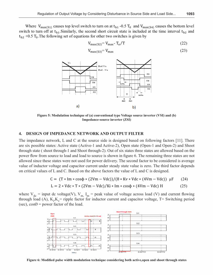
4 Design of Impedance network and output filter The impedance network, L and C at the source side is designed based on following factors [11]. There are six possible states: Active state (Active-1 and Active-2), Open state (Open-1 and Open-2) and Shoot through state ( shoot through-1 and Shoot through-2). Out of six states three states are allowed based on the power flow from source to load and load to source is shown in figure 6. The remaining three states are not allowed since these states were not used for power delivery. The second factor to be considered is average value of inductor voltage and capacitor current under steady state value is zero. The third factor depends on critical values of L and C. Based on the above factors the value of L and C is designed.
C = (T ∗ Im ∗ cosɸ ∗ (2Vm− Vdc))/(8 ∗ Kv ∗ Vdc ∗ (4Vm− Vdc)) µF (24)
L = 2 ∗ Vdc ∗ T ∗ (2Vm − Vdc) Ki ∗ Im ∗ cosɸ ∗ (4Vm− Vdc)⁄ H (25) where Vdc = input dc voltage(V), Vm ,Im =peak value of voltage across load (V) and current flowing through load (A), Ki,Kv= ripple factor for inductor current and capacitor voltage,T= Switching period (sec), cosØ = power factor of the load.
The predominant harmonic content present at the output of inverter is investigated and based on
that the relation between input voltage and output voltage is given by equation (25).
V= V ∗ 𝑋𝑐 (X − X )⁄ (25)
Using the above equation we can calculate L and C.
where XC Capacitive reactance= 1 2 ∗ pi ∗ f ∗ C⁄ , XL Inductive reactance= 2 ∗ pi ∗ f ∗ L
By fixing either L (or) C, calculation of other parameter can be done. By Equation (26)
V0,h =1-2% of Vin (26) where Vo,h is the harmonic output voltage of inverter. Here f is equal to harmonic frequency of
whose magnitude is higher. Similarly, the fundamental component of voltage across load is equivalent to 90% of input DC voltage.
S. Sabareswar, D. Kalyanraj and A. Stanley Jesudaiyan
1093
4
V()= V+ T T⁄ (20) V()= V (21)
Where V() causes top level switch to turn on at t -0.5 T and V() causes the bottom level switch to turn off at t.Similarly, the second short circuit state is included at the time interval t and t +0.5 T.The following set of equations for other two switches is given by
V()= V- T T⁄ (22)
V()= V (23)
Figure 5: Modulation technique of (a) conventional type Voltage source inverter (VSI) and (b) Impedance-source inverter (ZSI)
4 Design of Impedance network and output filter The impedance network, L and C at the source side is designed based on following factors [11]. There are six possible states: Active state (Active-1 and Active-2), Open state (Open-1 and Open-2) and Shoot through state ( shoot through-1 and Shoot through-2). Out of six states three states are allowed based on the power flow from source to load and load to source is shown in figure 6. The remaining three states are not allowed since these states were not used for power delivery. The second factor to be considered is average value of inductor voltage and capacitor current under steady state value is zero. The third factor depends on critical values of L and C. Based on the above factors the value of L and C is designed.
C = (T ∗ Im ∗ cosɸ ∗ (2Vm− Vdc))/(8 ∗ Kv ∗ Vdc ∗ (4Vm− Vdc)) µF (24)
L = 2 ∗ Vdc ∗ T ∗ (2Vm − Vdc) Ki ∗ Im ∗ cosɸ ∗ (4Vm− Vdc)⁄ H (25) where Vdc = input dc voltage(V), Vm ,Im =peak value of voltage across load (V) and current flowing through load (A), Ki,Kv= ripple factor for inductor current and capacitor voltage,T= Switching period (sec), cosØ = power factor of the load.
The predominant harmonic content present at the output of inverter is investigated and based on
that the relation between input voltage and output voltage is given by equation (25).
V= V ∗ 𝑋𝑐 (X − X )⁄ (25)
Using the above equation we can calculate L and C.
where XC Capacitive reactance= 1 2 ∗ pi ∗ f ∗ C⁄ , XL Inductive reactance= 2 ∗ pi ∗ f ∗ L
By fixing either L (or) C, calculation of other parameter can be done. By Equation (26)
V0,h =1-2% of Vin (26) where Vo,h is the harmonic output voltage of inverter. Here f is equal to harmonic frequency of
whose magnitude is higher. Similarly, the fundamental component of voltage across load is equivalent to 90% of input DC voltage.
Figure 5: Modulation technique of (a) conventional type Voltage source inverter (VSI) and (b) Impedance-source inverter (ZSI)
4. DESIGN OF IMPEDANCE NETWORK AND OUTPUT FILTER The impedance network, L and C at the source side is designed based on following factors [11]. There are six possible states: Active state (Active-1 and Active-2), Open state (Open-1 and Open-2) and Shoot through state ( shoot through-1 and Shoot through-2). Out of six states three states are allowed based on the power flow from source to load and load to source is shown in figure 6. The remaining three states are not allowed since these states were not used for power delivery. The second factor to be considered is average value of inductor voltage and capacitor current under steady state value is zero. The third factor depends on critical values of L and C. Based on the above factors the value of L and C is designed.
4
V()= V+ T T⁄ (20) V()= V (21)
Where V() causes top level switch to turn on at t -0.5 T and V() causes the bottom level switch to turn off at t.Similarly, the second short circuit state is included at the time interval t and t +0.5 T.The following set of equations for other two switches is given by
V()= V- T T⁄ (22)
V()= V (23)
Figure 5: Modulation technique of (a) conventional type Voltage source inverter (VSI) and (b) Impedance-source inverter (ZSI)
4 Design of Impedance network and output filter The impedance network, L and C at the source side is designed based on following factors [11]. There are six possible states: Active state (Active-1 and Active-2), Open state (Open-1 and Open-2) and Shoot through state ( shoot through-1 and Shoot through-2). Out of six states three states are allowed based on the power flow from source to load and load to source is shown in figure 6. The remaining three states are not allowed since these states were not used for power delivery. The second factor to be considered is average value of inductor voltage and capacitor current under steady state value is zero. The third factor depends on critical values of L and C. Based on the above factors the value of L and C is designed.
C = (T ∗ Im ∗ cosɸ ∗ (2Vm− Vdc))/(8 ∗ Kv ∗ Vdc ∗ (4Vm− Vdc)) µF (24)
L = 2 ∗ Vdc ∗ T ∗ (2Vm − Vdc) Ki ∗ Im ∗ cosɸ ∗ (4Vm− Vdc)⁄ H (25) where Vdc = input dc voltage(V), Vm ,Im =peak value of voltage across load (V) and current flowing through load (A), Ki,Kv= ripple factor for inductor current and capacitor voltage,T= Switching period (sec), cosØ = power factor of the load.
The predominant harmonic content present at the output of inverter is investigated and based on
that the relation between input voltage and output voltage is given by equation (25).
V= V ∗ 𝑋𝑐 (X − X )⁄ (25)
Using the above equation we can calculate L and C.
where XC Capacitive reactance= 1 2 ∗ pi ∗ f ∗ C⁄ , XL Inductive reactance= 2 ∗ pi ∗ f ∗ L
By fixing either L (or) C, calculation of other parameter can be done. By Equation (26)
V0,h =1-2% of Vin (26) where Vo,h is the harmonic output voltage of inverter. Here f is equal to harmonic frequency of
whose magnitude is higher. Similarly, the fundamental component of voltage across load is equivalent to 90% of input DC voltage.
where Vdc = input dc voltage(V), Vm, Im = peak value of voltage across load (V) and current flowing through load (A), Ki,Kv= ripple factor for inductor current and capacitor voltage, T= Switching period (sec), cosØ = power factor of the load.
Figure 6: Modified pulse width modulation technique considering both active,open and shoot through states
Regulation of Output Voltage by Considering Disturbance in Source Side and Load Side...

1094
The predominant harmonic content present at the output of inverter is investigated and based on that the relation between input voltage and output voltage is given by equation (25).
4
V()= V+ T T⁄ (20) V()= V (21)
Where V() causes top level switch to turn on at t -0.5 T and V() causes the bottom level switch to turn off at t.Similarly, the second short circuit state is included at the time interval t and t +0.5 T.The following set of equations for other two switches is given by
V()= V- T T⁄ (22)
V()= V (23)
Figure 5: Modulation technique of (a) conventional type Voltage source inverter (VSI) and (b) Impedance-source inverter (ZSI)
4 Design of Impedance network and output filter The impedance network, L and C at the source side is designed based on following factors [11]. There are six possible states: Active state (Active-1 and Active-2), Open state (Open-1 and Open-2) and Shoot through state ( shoot through-1 and Shoot through-2). Out of six states three states are allowed based on the power flow from source to load and load to source is shown in figure 6. The remaining three states are not allowed since these states were not used for power delivery. The second factor to be considered is average value of inductor voltage and capacitor current under steady state value is zero. The third factor depends on critical values of L and C. Based on the above factors the value of L and C is designed.
C = (T ∗ Im ∗ cosɸ ∗ (2Vm− Vdc))/(8 ∗ Kv ∗ Vdc ∗ (4Vm− Vdc)) µF (24)
L = 2 ∗ Vdc ∗ T ∗ (2Vm − Vdc) Ki ∗ Im ∗ cosɸ ∗ (4Vm− Vdc)⁄ H (25) where Vdc = input dc voltage(V), Vm ,Im =peak value of voltage across load (V) and current flowing through load (A), Ki,Kv= ripple factor for inductor current and capacitor voltage,T= Switching period (sec), cosØ = power factor of the load.
The predominant harmonic content present at the output of inverter is investigated and based on
that the relation between input voltage and output voltage is given by equation (25).
V= V ∗ 𝑋𝑐 (X − X )⁄ (25)
Using the above equation we can calculate L and C.
where XC Capacitive reactance= 1 2 ∗ pi ∗ f ∗ C⁄ , XL Inductive reactance= 2 ∗ pi ∗ f ∗ L
By fixing either L (or) C, calculation of other parameter can be done. By Equation (26)
V0,h =1-2% of Vin (26) where Vo,h is the harmonic output voltage of inverter. Here f is equal to harmonic frequency of
whose magnitude is higher. Similarly, the fundamental component of voltage across load is equivalent to 90% of input DC voltage.
where Vo,h is the harmonic output voltage of inverter. Here f is equal to harmonic frequency of whose magnitude is higher. Similarly, the fundamental component of voltage across load is equivalent to 90% of input DC voltage.
5. SIMULATION RESULTS
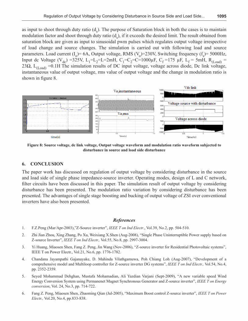
Figure 7 shows the closed loop simulation circuit of ZSI feeding RL load considering disturbance in the load side and source side. The closed loop simulation was carried out using the software MATLAB/SIM POWERSYSTEM. The circuit consists of dc voltage source, impedance network, switches, filter followed by load. Here, three different RL load is considered. Each acting at three different times with varying output voltage. To control the voltage at the inverter terminal, the steady state controller circuit was employed to generate the modulation index and shoot through duty ratio for PWM pulses. For this the actual voltage from inverter terminals is sensed and compared with rated rms load voltage rating. At the source side input dc voltage is varied by having three different sources at the input and in turn this is compared with reference dc link voltage.
Figure 7: Closed loop simulated power of single phase ZSI feeding RL load considering disturbance in the load side and source side
The error generated is given as input to PI controller which generates modulation index (ma) for controlling output voltage. Similar case is done with source side and the output of PI controller is given
S. Sabareswar, D. Kalyanraj and A. Stanley Jesudaiyan
1095
as input to shoot through duty ratio (ds). The purpose of Saturation block in both the cases is to maintain modulation factor and shoot through duty ratio (ds), if it exceeds the desired limit. The result obtained from saturation block are given as input to sinusoidal pwm pulses which regulates output voltage irrespective of load change and source changes. The simulation is carried out with following load and source parameters. Load current (Io)= 6A, Output voltage, RMS (Vo)=230V, Switching frequency (fs)= 5000Hz, Input dc Voltage (Vdc) =325V, L1=L2=L=2mH, C1=C2=C=1000µF, Cf =175 µF, Lf = 5mH, R(Load) = 23Ω, L(Load) =0.1H The simulation results of DC input voltage, voltage across diode, Dc link voltage, instantaneous value of output voltage, rms value of output voltage and the change in modulation ratio is shown in figure 8.
Figure 8: Source voltage, dc link voltage, Output voltage waveform and modulation ratio waveform subjected to disturbance in source and load side disturbance
6. CONCLUSION The paper work has discussed on regulation of output voltage by considering disturbance in the source and load side of single phase impedance-source inverter. Operating modes, design of L and C network, filter circuits have been discussed in this paper. The simulation result of output voltage by considering disturbance has been presented. The modulation ratio variation by considering disturbance has been presented. The advantages of single stage boosting and bucking of output voltage of ZSI over conventional inverters have also been presented.
References1. F.Z.Peng (Mar/Apr-2003),”Z-Source inverter”, IEEE T on Ind Electr., Vol.39, No.2, pp. 504-510.
2. Zhi Jian Zhou, Xing Zhang, Po Xu, Weixiang X.Shen (Aug-2008), “Single Phase Uninterruptible Power supply based on Z-source Inverter”, IEEE T on Ind Electr., Vol.55, No.8, pp. 2997-3004.
3. Yi Huang, Miaosen Shen, Fang Z. Peng, Jin Wang (Nov-2006), “Z-source inverter for Residential Photovoltaic systems”, IEEE T on Power Electr., Vol.21, No.6, pp. 1776-1782.
4. Chandana Jayampathi Gajanayake, D. Mahinda Vilathgamuwa, Poh Chiang Loh (Aug-2007), “Development of a comprehensive model and Multiloop controller for Z-source inverter DG systems”, IEEE T on Ind Electr., Vol.54, No.4, pp. 2352-2359.
5. Seyed Mohammad Dehghan, Mustafa Mohamadian, Ali Yazdian Varjani (Sept-2009), “A new variable speed Wind Energy Conversion System using Permanenet Magnet Synchronous Generator and Z-source inverter”, IEEE T on Energy conversion, Vol. 24, No.3, pp. 714-722.
6. Fang Z. Peng, Miaosen Shen, Zhaoming Qian (Jul-2005), “Maximum Boost control Z-source inverter”, IEEE T on Power Electr., Vol.20, No.4, pp.833-838.
Regulation of Output Voltage by Considering Disturbance in Source Side and Load Side...

7. Quang-Vinh Tran,Tae-Won Chun, Jung -Ryol Ahn, Hong -Hee Lee (Oct-2007), “Algorithms for controlling Both the DC-Boost and AC output voltage of Z-source inverter”, IEEE T on Ind Electr., Vol.54, No.5, pp. 2745-2750.
8. Sumedha Rajakaruna, Laksumana Jayawickrama (Jul-2010), “Steady state analysis and designing impedance network of z-source inverters”, IEEE T on Ind Electr., Vol.57, No.7, pp. 2483-2491.
9. Poh Chiang Loh, Member, IEEE, D. Mahinda Vilathgamuwa, Senior Member, IEEE, Yue Sen Lai, Geok Tin Chua, and Yunwei Li, Student Member, IEEE (Nov-2005),” Pulse-Width Modulation of Z-Source Inverters”, IEEE T on Power Electr., vol. 20, No. 6.
S. Sabareswar, D. Kalyanraj and A. Stanley Jesudaiyan1096