On leakage power optimization in clock tree networks for ...

1
Abstract—Synchoros VLSI design style has been proposed as an
alternative to standard cell-based design. Standard cells are
replaced by synchoros large grain VLSI design objects called
SiLago blocks. This new design style enables end-to-end
automation of large scale designs by abutting the SiLago blocks to
eliminate logic and physical synthesis for the end-users. A key
problem in this automation process is the generation of regional
clock tree. Synchoros design style requires that the clock tree
should emerge by abutting its fragments. The clock tree fragments
are absorbed in the SiLago blocks as a one-time engineering effort.
The clock tree should not be ad-hoc, but a structured and
predictable design whose cost metrics are known. Here, we present
a new clock tree design that is compatible with the synchoros
design style. The proposed design has been verified with static
timing analysis and compared against functionally equivalent
clock tree synthesised by the commercial EDA tools. The scheme
is scalable and, in principle, can generate arbitrarily complex
designs. In this paper, we show as a proof of concept that a regional
clock tree can be created by abutment. We prove that with the help
of the generated clock tree, it is possible to generate valid VLSI
designs from 0.5 to ~2 million gates. The resulting generated
designs do not need a separate regional clock tree synthesis. More
critically, the synthesised design is correct by construction and
requires no further verification. In contrast, the state-of-the-art
hierarchical synthesis flow requires synthesis of the regional clock
tree. Additionally, the conventional clock tree and its design needs
a verification step because it lacks predictability. The results also
demonstrate that the capacitance, slew and the ability to balance
skew of the clock tree created by abutment is comparable to the
one generated by commercial EDA tools.
Index Terms— CGRA, Clock Tree Synthesis, Composition by
Abutment, EDA, VLSI Design, SiLago, Synchoricity
I. INTRODUCTION
n this paper, we present a clock tree generation scheme for a
novel synchoros VLSI (Very Large Scale Integration)
design framework. Synchoros VLSI design is an alternative
to the standard cell-based VLSI design framework. The word
synchoros is derived from the Greek word for space – χώρος
(khôros). Synchoricity is analogous to synchronicity. In
synchronous systems, time is discretised with clock ticks to
enable temporal composition of synchronous datapaths. In
synchoros systems, space is discretised uniformly with a virtual
grid. This virtual grid enables the spatial composition of the
system by abutting synchoros building blocks, that we call
SiLago (Silicon Lego bricks) blocks. All wires, including the
clock, are absorbed within the SiLago blocks. When a system
is composed by abutting SiLago blocks, a valid DRC (Design
Corresponding author
Rule Checking) and timing clean GDSII (Graphic Database
System II) is generated. The design does not need any further
VLSI engineering, other than what has gone into creating the
SiLago blocks as a one-time engineering effort. In essence,
SiLago blocks are the new mega standard cells.
The need for synchoros VLSI design style, as a replacement
for standard-cell-based VLSI design, is elaborated in section II.
Briefly, the key benefits of synchoros VLSI design style are:
1. End-to-end automation of complex system-models to
GDSII; complex system models imply 100+ million gate
complexity and non-deterministically concurrent untimed
applications
2. Computational efficiency similar to application-Specific
Integrated Circuit (ASIC) [1]
3. Programming comparable engineering effort with correct-
by-construction and near-perfect prediction of cost metrics,
4. Sufficient flexibility for in-field bug fixes and version
updates
5. Foundry compatible design
6. Potential to eliminate mask engineering cost and
significantly lower silicon and engineering cost related to
DFT (Design For Test).
Clocks in synchoros VLSI designs have three levels of
hierarchy. In the highest level of hierarchy is the global clock
that is derived from PLL and distributed to region instances.
The region instances roughly correspond to chiplets or sub-
systems in traditional SOC architectures. They communicate
with each other on a latency insensitive basis. Each region
instance is composed of SiLago blocks that communicate with
each other on a synchronous basis fed by a regional clock tree
(RCT). RCT is the focus of this paper and constitutes the second
level on the hierarchy of clocks. The lowest level of the
hierarchy is the clock tree in the Silago block, which is
synthesised by commercial EDA tools.
In this paper, we focus on a critical aspect of synchoros VLSI
design style – the generation of valid RCT by abutment of
SiLago blocks. The proposed RCT generation-by-abutment
scheme does not compete with the existing clock tree synthesis
schemes on traditional figure-of-merits. Instead, the proposed
scheme obviates the need for RCT synthesis.
The key contributions in this paper are:
a. We present a design that allows the RCT to be divided into
fragments that are absorbed as part of the synchoros SiLago
blocks. When these blocks abut, a valid RCT gets created.
No additional step, like clock tree synthesis of the traditional
standard cells based design flow, is needed.
b. The generated RCT and the synchoros SiLago based design
is correct-by-construction and does not require any further
Regional Clock Tree Generation by Abutment in
Synchoros VLSI Design Dimitrios Stathisa,, Panagiotis Chaourania, Syed M. A. H. Jafria, Ahmed Hemania
aKTH Royal Institute of Technology, Electrum 229, 164 40 Kista, Stockholm, Sweden
Email: stathis, pancha, jafri, [email protected]
I

2
verification by static timing analysis or DRC.
c. The generated RCT is predictable in terms of its switching
capacitance, arrival time, slew and skew at each leaf node,
i.e., the SiLago block.
d. The generated RCT has comparable cost metrics -
capacitance, skew and slew- to a functionally equivalent
RCT generated by commercial EDA tools.
The roadmap for the rest of the paper is as follows: In the
next section II, we justify the need for synchoros VLSI design
style as a replacement for standard cell-based VLSI design. In
section III, we introduce a synchoros VLSI design platform as
the background in which the proposed RCT scheme has been
developed. In the same section, we also introduce the demands
for RCT generation in a synchoros VLSI design platform.
Sections II and III give an overview of the basics of the
synchoros VLSI design style and serve as the motivation and
basis for this work. In section IV, we elaborate the proposed
RCT generation-by-abutment scheme, and in section V, we
explain the process of configuring the RCT. In section VI, we
quantify the benefits and cost of RCT, compare it to a
functionally equivalent clock tree generated by commercial
EDA tools and provide proof-of-concept experimental results
for the predictability of the generated RCT. In section VII, we
review the state-of-the-art in clock tree synthesis and argue why
these techniques do not meet the requirements for RCT
generation in the synchoros VLSI design style. Finally, we
conclude and point to the ongoing enhancements of the SiLago
platform.
II. THE NEED FOR SYNCHOROS VLSI DESIGN
Synchoros VLSI design style is needed to make ASIC-like
performance and computational efficiency affordable to even
small actors. This is made possible by enabling end-to-end
automation and eliminating the need for logic and physical
synthesis by the end-user. The problem addressed in this paper
is a critical sub-problem in enabling synchoros VLSI design
style.
ASICs outperform software-based implementations by 2-3
orders [2]. The need for ASIC-like efficiency is acutely felt in
all domains of the industry[3 - 8]. The principal reason for not
adopting ASICs has been the large cost, of which 90% is
engineering [12]. Furthermore, designing ASIC requires
specialist competence, expensive and difficult to use EDA tools
and a long lead time. All these factors add up to ASICs being
accessible only to large actors like Google, that opted for an
ASIC style implementation for its TPU. Even making an
accelerator rich and software-centric custom SOC is too
expensive for small actors. As a result, small actors are forced
to adopt FPGAs and GPUs that seldom deliver the required
power-performance [13].
A. Challenges with state-of-the-art EDA flows
We next analyse why standard cell-based EDA flows have
not scaled with complexity. This analysis is done in terms of the
VLSI design space, shown in Fig. 1. We argue that this design
space increases exponentially with complexity and impedes
design automation. The key contributions of the synchoros
design style are a) to sufficiently reduce this design space and
b) to make this reduced design space composable and
predictable. These contributions enable end-to-end design
automation of complex applications and systems. The final
custom design has ASIC comparable performance and
efficiency.
The VLSI design space that is shown in Fig. 1 has three
dimensions. Abstraction and complexity are the independent
variables, and the number of solutions is an exponential
function of the two independent variables. There are six levels
of abstraction, as shown in Fig. 1. Synthesis is the process of
refining from more abstract to more detailed and proceeds in a
top-down manner, by successively refining the functionality
from one level to the next lower level. At each level, the
refinement process evaluates multiple functionally equivalent
implementation alternatives. These implementations are
expressed in terms of building blocks at the next lower level of
abstraction. As this process continues the number of design
alternatives increases exponentially at each level, as shown in
Fig. 1. By the time physical synthesis happens, the design space
has expanded to (((TL)R)A)P. Complexity C further increases this
space to (((TL)R)A)P)C.
The top-down refinement process implies that the real cost
of a design is not known until it has been refined down to the
physical level. At higher abstractions, when multiple solutions
are evaluated, the evaluations are based on estimated cost-
metrics. The accuracy of these estimates degrade with
increasing abstraction level and complexity of the functionality.
Fig. 1. Design space comparison between different VLSI style
Log (# of Solutions)
Physical LevelGDSII
BooleanStd. Cells
Algorithm
SystemNon-deterministically concurrent
and communicationg applications
ApplicationHierarchy of Algorithms
RTL
Standard
Cells
Synchoros
VLSI DesignAP
(RA)P
((LR)A)P
R
A
P
P
L
T
HLS
(a) Full Custom
Standard CellsPhysical Level
(b) Standard Cell
Standard Cells
Synchoros VLSI
GDSII for
Logic +Wires
(c) Basic Synchoros
VLSI Platform
Standard Cells
Synchoros VLSI
GDSII for
Logic +Wires
FIMPs
(d) Synchoros VLSI
Platform after HLS
Fu
nc
tio
n V
eri
fic
ati
on
(F
V)
Co
ns
tra
ints
Ve
rifi
ca
tio
n (C
V)
Au
tom
ate
d
SL
S +
AL
S
FIMP/GDSII
System-Level
Au
tom
ate
d
On
etim
e E
ngin
eerin
g
Effo
rtNo need
for
FV & CV
Au
tom
ate
d
Logic
/Ph
ysic
al
Syn
theses
Physical Design
RTL
Man
ual
Sys
tem
Arc
hite
ctin
g
System-Level
Physical Design
Man
ual
Syste
m A
rch
itectin
g
System-Level
Logic
Synthesis
Physical
Synthesis
SLS
HLS
ALS
HLS : High-Level Synthesis
FIMP : Function Implementation
SLS : System-Level Synthesis
ALS : Application-Level Synthesis
FV : Function Verification
CV : Constraints Verification
(TL)R
TL
T
((TL)R)A
(((TL)R)A)P

3
This exponential increase in design space and the exponential
degradation in accuracy of cost-metrics, which are used to
explore the design space, together with an increase in
abstraction and complexity is the fundamental VLSI design
challenge. All progress in VLSI design automation can be cast
in terms of attempts to solve the fundamental VLSI design
challenge.
In the full-custom era, shown in Fig. 1a, the entire design
space from the system down to the physical level was manually
refined. Despite Mead Conway’s structured VLSI design style
[14] and later attempts to automate the process using silicon
compilers. The full custom design space was too large for
design automation. This restricted the design to 𝒪(10K) gates.
Standard cells were introduced to reduce the design space
and to enable a higher degree of automation. That allowed the
complexity of the systems to go beyond what was possible with
full-custom design style. The reduction of the design space was
achieved by standardising all boolean level logic as a set of one-
time engineered set of standard cells. This effectively raised the
physical design to boolean level, i.e., as soon as a design is at a
boolean level, we know its physical design. However, the wires
that connect these standard cells, clock them, reset them etc. are
not known. They have to be synthesised as part of physical
synthesis. In synchoros VLSI design style all wires, functional
and infrastructural, get created by abutment rather than in a
follow-up physical synthesis step.
Despite imperfectly raising the physical design to boolean
level, standard cells succeeded in automating synthesis from
RTL down to physical level. The Achilles heel of the standard
cell design flow is that the refinement from system-level down
to RTL is done manually. For ASICs, this refinement is in terms
of functional RTL designs, and for SOCs, this refinement is in
terms of infrastructural IPs. This manual refinement requires
costly functional verification to ensure that the system model is
preserved in the manually refined RTL model. Furthermore,
manual refinement is done using crude estimates that can only
be verified when the design has been refined down to the
physical level. The final verification of the design is shown as
constraint verification in Fig. 1b. The functional and constraint
verification are not independent and are the dominant cost
components that make complex VLSI design in standard cells
unaffordable.
High-level synthesis has been intensely researched for the
last three decades to increase automation beyond RTL and thus
reduce manual refinement. However, it is still not mainstream;
as recently as 2016, the status of HLS was judged as [15]:
“Could High-Level Synthesis be the key to the next generation
of EDA? As we all know, that did not happen—despite some
very large investments”. HLS, in short, is a victim of the
fundamental VLSI design challenge discussed earlier. This
rules out synthesis of ASIC-like custom hardware from even
higher abstractions: application and system levels.
B. Synchoricity to the rescue
Synchoricity solves the challenges discussed above by
borrowing two core ideas from the two previous generations of
VLSI Design Style. The idea that is borrowed from the standard
cells is to reduce the design space by raising the physical design
to RTL, as shown in Fig. 1c. The concept of composition by
abutment is borrowed from the Mead-Conway structured VLSI
design methodology for full-custom designs. Using the
composition by abutment, all wires are created by abutting the
RTL standard cells that we call SiLago (Silicon Lego) blocks.
As a result, once the functionality is defined in terms of RTL
operations exported by the SiLago blocks, the physical design
of logic and also wires is known. The physical design is created
by simple abutment of the SiLago blocks and without any need
for logic and physical synthesis. This effectively raises the
physical design to RTL for both logic and wires and has the
effect of exponentially reducing the design space. as shown in
Fig. 1c. Synchoricity and composition by abutment makes this
reduced space predictable and composable. This empowers
HLS, the synthesis from algorithms because the physical design
is just one abstraction lower at RTL. This is exploited to build
a library of implementations of function libraries (BLAS,
LinPack, Matlab toolboxes etc.) in varying dimensions and
degrees of parallelism. By building a library of standardised
functions and implementations, the design space can be further
reduced, as shown in Fig. 1d, and the physical design can be
effectively raised to the algorithmic level. This significantly
reduced design space enables automation from system and
application levels. Automation has two benefits. Firstly, it
enables the synthesis of custom ASIC-like design, and
secondly, it provides correct-by-construction guarantee that
eliminates the functional verification. The constraint
verification is also eliminated because synchoricity makes the
reduced design space predictable with post-layout accuracy.
We refer the reader to [16] for an early version of application-
level synthesis and how it differs from HLS.
We close this section with Table I, where we compare the
standard cells with the synchoros VLSI design styles and show
how the former overcomes the limitations of the latter.
TABLE I
STANDARD CELLS VS SYNCHOROS DESIGN
Standard Cells Synchoros VLSI Design
Physical design atomic building blocks
All designs are composed in terms
of Standard cells, that are atomic physical design building blocks
that implement Boolean
operations.
All designs are composed in terms
of domain-specific SiLago blocks that are atomic physical design
building blocks that implement
RTL operations.
Physical Design raised to higher abstractions
The dimension and position of
every intra standard-cell wire segment is known, when the design
is at the Boolean level.
A follow-up physical synthesis is required to implement inter
standard cell wires and buffers.
When a design is at RTL level,
dimension and position of every intra and inter SiLago Block
transistor and wire-segment is
known. This advantage over standard cell is enabled by the
Synchoricity property of the
SiLago blocks.
Reduction in VLSI Design Space
Reduces VLSI design space from (((TL)R)A)P to ((LR)A)P.
Reduces VLSI design space from (((TL)R)A)P to (RA)P.
The reduction in design space
enables partial automation from
RTL to Physical level; system-level to RTL refinement remains
manual.
The reduction in design space
enables end-to-end automation
from system-level to RTL that is equivalent to being at Physical
level (GDSII).
III. THE SYNCHOROUS VLSI DESIGN FRAMEWORK
In this section, we present an experimental synchoros VLSI

4
design framework. This framework forms the basis for arguing
why a new method for RCT (Regional Clock Tree) generation
by abutment is needed. Even though is not focus of this paper,
all inter-SiLago wires and not just RCT are created by abutting
SiLago blocks. We next briefly discuss the salient points about
this experimental synchoros VLSI design framework.
A. Synchoros SiLago Blocks and Composition by Abutment
SiLago blocks are synchoros, i.e., their spatial dimensions
are discrete in terms of the virtual grid cells, as shown in Fig. 4.
Composition by abutment is enabled by bringing all the inter-
SiLago block interconnects (functional and infrastructural
wires like clock, power grid, etc.) to the periphery, at the right
place and on the right metal layer. As a result, when
functionally compatible SiLago blocks are placed on the grid,
their corresponding interconnect points abut to create a larger
valid VLSI design. The alignment of the interconnect points
happens without any further need for VLSI engineering, other
than what has already gone into creating the SiLago blocks, see
Fig. 2. We note that Lego bricks are also synchoros and enable
the creation of an arbitrarily complex system by abutting the
Lego bricks.
B. Regions: Domain-specific SiLago Blocks
SiLago blocks are heavily customised for specific
application domains called regions. There are two broad
categories of regions: functional and infrastructural. Fig. 3
shows examples in these two categories. Functional region
types roughly correspond to the dwarfs identified in the
Berkeley Report on Landscape of Parallel Computing [17].
Functional regions are domain-specific Coarse Grain
Reconfigurable Architectures (CGRAs). These CGRAs are
customised for their respective domains for computation,
control, address-generation, regional-interconnect, access to
scratchpad etc. Differentiation of SiLago CGRAs compared to
others is elaborated in [1]. Evidence of these CGRAs achieving
power and performance comparable to ASICs that is typically
3-5 orders higher than GPUs is provided in [9, 11, 1].
C. The generality of synchoros VLSI design framework
Synchoros VLSI design style is as general as the standard
cell-based design style. This claim is predicated on the
assumption that a finite set of regions can cover the functional
and infrastructural needs of any arbitrary application or system.
This is also the implicit assumption in the Berkeley report [17]
and the library based development environments like Matlab
and Simulink. The regions listed in Fig. 3 should be sufficient
for most applications and systems. We anticipate, most systems
would require multiple region instances of different types.
However, should there be a domain that is not covered by the
regions shown in Fig. 3a, it is not a fundamental limitation of
the synchoros VLSI design style that it is not there, it is merely
a question of an extra one-time engineering effort to create such
a region. For instance, if a standard cell library lacks Mueller−C
standard cell, it may be hard to implement handshake protocol.
However, this is not a fundamental limitation of the standard
cell-based design style. A one-time effort to design a
Mueller−C standard cell would be sufficient. We also
emphasise that the synchoros VLSI design style is not restricted
to compile-time static data-parallel applications. We also target
reactive, non-deterministically concurrent and communicating
applications.
D. Three Levels of Hierarchy
In the synchoros VLSI design framework, there are three
levels of hierarchy: local, regional and global, see Fig. 3b. The
design of the clock distribution network is also divided into
three levels, see Fig. 4. The synchoros grid in Fig. 4 enforces
synchoricity. Each hierarchy level uses a different clock
distribution mechanism.
Local: At the local level, i.e., the intra-SiLago block level, all
wires – functional and infrastructural – are designed ad-hoc and
synthesized by the commercial EDA tools. The same way they
are done in standard cell-based design flows. In this case, the
local clock tree (LCT) is also synthesized by the EDA tools.
Regional: Region instances are aggregation of region specific
SiLago blocks. All inter-SiLago block wires in a region
instance are created by abutment. SiLago blocks communicate
with each other via local region specific NOCs, see [20-24].
Regional Clock Trees (RCT) are design constructs that are
absorbed in each SiLago block. When SiLago blocks in a region
instance abut, an RCT gets created that feeds the LCTs in each
SiLago block by balancing the skew and in the same time
maintaining the slew rate.
Global: The global level is the chip level and is composed of
region instances, also composed by abutment. Region instances
communicate with each other using global NOCs, see [1] for
more details. These global NOCs are composed of SiLago
blocks for buffered wires, NOC logic and region specific
network interface units. Region instances communicate with
each other on latency insensitive basis using a variant of GALS,
called Globally Ratiochronous and Locally Synchronous
(GRLS) method. For more details we refer the reader to [25].
The Global Clock derived from PLL(s) is distributed via the
space allocated for global NOCs. It is used to feed the RCTs in
each region instance via a GRLS interface at region instance
Fig. 2. Composition by abutment of SiLago blocks
Fig. 3. SiLago platform hierarchy
Power Stripes
Po
we
r S
trip
es
Internal Power Rings
Infr
astr
uctu
re/r
ou
tin
g w
ire
s
Standard cell
core area
Abutable RCT
Connection by abutment
Region Types – SiLago Block Types
Functional
Dense Linear Algebra
Sparse Linear Algebra
Inner Modem
Outer Modem
Graph Theory
Protocol Processing
Spectral Methods
Dynamic Programming
State Machines
Infrastructural
NOCs
Scratch Pad Memory
PLL + CGU
Memory Controller
FIFO, FIFO Controller
RISC Processors
DMA
Memory Consistency
Power Management
Synchoros SiLago Design Instance
O(10s-100s) million gates
Region
Instance 1
SiLago
Block
Instance 1
Region
Instance 2
Region
Instance m
SiLago
Block
Instance 2
SiLago
Block
Instance n
. . .
. . .
Region instances are O(1-10) million gates
SiLago Blocks are typically 10-200 K gates
(a) Functional and Infrastructural Region Types (b) Three Levels of hierarchy in
Synchoros SiLago VLSI Design Platform
Global
Regional
Local

5
boundaries. Often the GRLS interface is absorbed as part of a
region specific network interface unit.
E. Overview of Synchoros VLSI Design Flow
The synchoros VLSI design flow has three components, as
shown in Fig. 5. Two of these components are a one-time
engineering effort, and the third component is used by the end-
user. The first component is responsible for the development of
the Synchoros SiLago platform. This methodology component
is based on commercial EDA tools. SiLago region types are
designed at RTL, verified, synthesised down to physical level,
made synchoros, abutment-ready and characterised with post
layout data, see [26]. The result is a library of synchoros SiLago
block types, the leaf nodes in Fig. 3b. The RCT fragment in
each SiLago block type is designed and incorporated during this
phase, as shown in Fig. 5.
The second component develops a library of function
implementations or FIMPs using SiLago HLS tool. The HLS
implements each function/algorithm/actor that could be used to
compose application or system models in M different
architectures. Each one of these M implementations employs
different degrees of parallelism, with different cost metrics
(area, latency and average energy). For instance, FIMPs for
2048 point FFT actor could vary in number and type of
butterflies. The libraries developed correspond to BLAS,
LinPACK, Matlab toolboxes etc.
The third component transforms the application and system
models composed in terms of actors/functions to custom
synchoros design in terms of SiLago blocks. At present a proof-
of-concept application-level synthesis tool exist, see [16] and
we are in the process of enhancing it to system-level synthesis.
With the above background on the experimental synchoros
VLSI design framework, we are ready to elaborate the design
of the RCT fragment in SiLago blocks that enable composition
by abutment.
IV. RCT BY ABUTMENT IN SYNCHOROS VLSI DESIGN
In this section, we elaborate the RCT design scheme. We first
lay down the requirements of synchoros VLSI design in sub-
section IV.B, with which the RCT design must comply. After
the requirements, we elaborate the RCT scheme in terms of its
components in sub-section IV.C. Next, in sub-section IV.D, we
elaborate the delay model of the RCT that is generated as a one-
time activity, as part of the design of synchoros VLSI platform.
We then explain how the delay model is used during application
and system-level syntheses. Finally, we present a method for
minimising the difference in the arrival of RCT in each SiLago
block’s LCT and present its solution in section V..
A. RCT Requirements in Synchoros VLSI Design
Regional clock tree (RCT) synthesis, like any other clock tree
synthesis, has two constraints. The first is to minimise the clock
skew, to maximise the percentage of clock period that can be
used by the combinational logic. The second is to maintain
sufficient drive strength to ensure that the slew rate, a
technology-design-rule, is not violated. The latter constraint is
critical because the timing models are characterised for a tight
range of slew rates. If this range is violated, the timing model
would no longer be valid. Finally, such a clock tree should
factor in variations in manufacturing, temperature and power
supply. Besides these standard requirements on RCT that all
clock trees must fulfil, there are two new requirements imposed
by the synchoros VLSI design. The RCT generated by abutment
must additionally fulfil the following two constraints:
1) Space Invariance
All SiLago blocks of the same type should have identical
electrical properties: delay, load, drive etc. This requirement
stems from the need to make the cost metrics of a synchoros
VLSI design predictable for the syntheses tools. A signal that
propagates through a SiLago block of a specific type should
have the same characteristics regardless of its location in the
fabric. If this requirement is not fulfilled, the same SiLago
block type would have to be characterised for each possible
location in the fabric. Such an engineering effort would be un-
scalable.
2) No follow-up VLSI engineering after abutment
The second requirement is that when SiLago blocks abut, the
RCT fragments should compose into a valid RCT tree. This
should happen without having to do any further synthesis of
wires, buffers or verification in terms of static timing analysis
(STA) or DRC (Design Rule Check).
Fulfilling these two requirements is the key contribution of
this paper. In the next sub-section, we present the RCT design
scheme that achieves these requirements.
B. RCT for Synchoros VLSI Design Style
Every SiLago block has an RCT fragment that includes three
components. These components enable a scalable, correct-by-
construction RCT to emerge by abutment of the RCT
fragments.
1) Standardised Entry and Exit Points
Every SiLago block type has standard entry (Hin, Vin) and exit
(Hout, Vout) points for the RCT fragment, as shown in Fig. 6.
Standard implies fixed location on specific edges and metal
Fig. 4. A SiLago design instance and the three levels of clock trees.
Fig. 5. SiLago synchoros design framework.
GR
LS
LCT LCT LCT
GR
LS
LCT LCT LCT LCT LCT
LCT LCTLCT LCTLCT
GR
LS
LCT LCT LCT
LCT LCTLCT LCTLCT
LCT LCT
LCTLCT
LCT LCT
LCT
LCTPLL RISCV
GRLS
GCT
Global Clock TreeRCT
Regional Clock TreeLCT
Local Clock Tree
Tw
o fu
nctio
nal
regio
n in
sta
nces
Inte
r-R
egio
n I
nsta
nce c
om
munic
ation
is o
n late
ncy insensitiv
e b
asis
usin
g G
RL
S p
roto
co
l
(Glo
bally
Ratiochro
nous L
ocally
Synchro
nous)
Third functional region instance
Region Specific
Network Interface Unit
SiLago Block with GRLS Interface NOC wires SiLago BlocksNOC
Logic SiLago Block
Synchoros grid lines
On
e T
ime E
ng
ineeri
ng
Eff
ort
c
Synchoros SiLago
Platform
EDA Tools
RCT Fragments
absorbed in SiLago
BlocksGDSII Macro Reports
FIMP Library(HLS)
M FIMPs for every
function
FIMP =
Function IMPlementation
1
2
3
End
to E
nd
auto
ma
ted
de
sig
n flo
w u
se
d b
y e
nd
use
r
Abutment Process to create the RCT and other wires
and configure the RCT tap selection
Compose GDSII Macro
Application Model
L Functions/Actors
Constraints
Energy, Performance, Area
1. Select Optimal Solution from ML solutions
2. Global Interconnect, buffers and control
3. Floorplanning
Number and types of SiLago blocks + Mapping

6
layers. The entry and exit points of RCT fragments in
neighbouring SiLago blocks abut to create a valid RCT. Since
the neighbours can be in horizontal, vertical, or both
dimensions, SiLago blocks need entry and exit points on both
horizontal and vertical edges as shown in Fig. 6.
RCT can be distributed/propagated in four orientations: top-
down and left-right, top-down and right-left, bottom-up and
left-right and bottom-up and right-left. The choice of
orientation depends on the corner at which the GCT (Global
Clock Tree) enters. The decision at which corner the GCT
enters depends on the number and floor planning of the global
NOCs during the application and system level syntheses
decisions. As stated earlier in section II, the GCT is routed in
the same physical space as the Global NOCs.
The entry point on the top-left corner of the fabric is selected
to ensure that the regional clock tree can connect with the global
clock tree in a regular fashion. The different SiLago blocks can
vary in size, but due to synchoricity, the size is discrete and
standardised, see Fig. 4. This synchoros property of the SiLago
blocks allow for blocks of different size to abut and generate a
valid regional clock tree, see Fig. 2.
2) Multiplexed and buffered horizontal and vertical chords
These components have two functions. The first is to select
RCT input and output, and the second is to maintain the slew
rate. Selecting the input implies selecting the Hin or Vin, as
shown in Fig. 6. The two inputs are fed to an OR gate. Only one
of the inputs can be a clock, and the other is set to zero when
configuring the RCT at the power-up time. Selecting the output
implies selecting if RCT is to be propagated to the right exit
(Hout), or the bottom exit (Vout), or both. The unselected exit is
set to 0 not to leave any hanging wires. This is achieved using
two AND gates, as shown in Fig. 6. Depending on the
configuration of the two AND gates, one of the four variants of
chord delay, TRCT_chord gets selected, see Fig. 6. These gates also
serve as the drivers to maintain the slew of the clock.
3) Programmable Delay Line
The third component is a programmable delay line that
enables adjusting the delay to the LCT entry point, see Fig. 6.
The delay is adjusted according to the position of the SiLago
block in a region instance with respect to where the GCT enters
the instance. The objective of adjusting the delay is to minimise
the skew of the arrival of the RCT at the LCT entry points, in
SiLago blocks in a region instance. The delay is adjusted by
selecting a tap with index i in the delay line, shown in Fig. 6.
The selected tap i introduces a delay ttap_i between the RCT and
LCT entry points.
The three components together are called RCT fragment and
the design of the RCT fragments in all SiLago block types is
identical. Depending on the size of the SiLago block type, the
length and position of the horizontal and vertical chords, and if
required the drive strength of the OR gate to maintain the slew,
can differ from one SiLago block type to another. The small and
simple logic in RCT fragment is built from standard cells and
does not require any custom design.
The LCT (Local Clock Tree) is automatically generated by
the EDA tools and can be different from one SiLago block type
to another. However, all SiLago bock instances of a specific
type will have identical LCTs.
The RCT fragment along with the rest of the logic, wires and
buffers in a SiLago block is hardened and characterised with
post layout data. The hardening process ensures synchoricity,
where SiLago blocks occupy multiples of SiLago grid cells. All
interconnect wires of each SiLago block, including those for
RCT fragments, are brought to the right positions and the right
metal layer to enable composition by abutment. As stated, this
is a one-time engineering effort and needs to be done once for
each type of SiLago block. The hardened SiLago blocks can
then be instantiated in any position in a SiLago region instance
of any permissible size.
We next derive the RCT delay model that enables calculating
the delay of an arbitrary RCT created by abutting the RCT
fragments without having to do STA (Static Timing Analysis).
This timing model is also used to decide the permissible size of
a region instance and the tap index i in each SiLago block. The
selection of the index i for each instance is done to minimise the
skew between the arrival of RCT at LCT entry points in SiLago
blocks in a region instance.
C. RCT Delay Model
The main delay that we are interested in is the latency of the
regional clock tree (RCT). The RCT latency is starting from the
entry point of a region instance and ends to each of the local
clock tree (LCT) entry points in the SiLago blocks, see Fig. 7.
There will be as many instances of this latency, as the number
of SiLago blocks in the region. The notation used for this
latency is TLCT_x,i. The subscript x identifies the node id and
subscript i identifies the selected tap index of the programmable
delay line in node x. The purpose of the programmable line is
to make all TLCT_x,i as equal as possible for every node x.
Balancing all TLCT_x,i keeps the skew within the limits of the
SiLago block’s slack, to not cause any timing violation. TLCT_x,i
has two components, listed below:
1. One is the sum of delays, TRCT_chord(s), in RCT chords in
nodes that precede the node x. This delay is called the
natural propagation delay of RCT, Tnat_x. Fig. 7 shows Tnat_6
as the thick red line composed of RCT chords in previous
nodes 0, 4 and 5.
2. The second component is the delay that is imposed on RCT
by the delay line in the destination node. This imposed delay
in the destination node n is represented by ttap_i,x, where i is
the tap index. ttap_i,x is itself made up of three components
and defined in Fig. 6. In the example shown in Fig. 7 node
6 is the destination node and ttap_i,6 is shown as the thick
Fig. 6. Hardened SiLago block and its integrated RCT fragment and its
components
SiLago Block Delay Notation
TRCT_chord TV_to_V, TV_to_H,TH_to_H, TH_to_V
Four variants of delay through
horizontal and vertical chords
TV_to_DL,
TH_to_DL
Delay of the wire connecting the Vin or
Hin and the Delay Line Entry Point
TDL_i
Delay imposed by delay line
depending on the index i
Tmux_i
Propagation delay through the mux
depending on the i index
ttap_i
Delay between the Vin or Hin and the
LCT Entry Point associated with the
selected tap i of the Delay Line
ttap_i = [ TH_to_DL | Tv_to_DL ] +
TDL_i + Tmux_i
Ttap
Set of delays associated with taps in
the Delay Line
{ttap_0,…, ttap_i,…, ttap_(M-1)}In each node, one and only one tap ttap_i
Ttap is selected by configuring the index i
De
lay
Lin
e
Local
Clock
Tree (LCT)
0|1
0|1.
VinHin
Hout
Vout
Horizontal Chord
Vertical
Chord
LCT Entry
Point
Delay Line
Entry Point
TD
L,i
Dela
y L
ine
(DL
)tap0
tap1
tapM-1
tap2
Tm
ux
i

7
green line.
𝑇𝑛𝑎𝑡_𝑥 = ∑ 𝑇𝑅𝐶𝑇_𝑐ℎ𝑜𝑟𝑑
𝑛𝑜𝑑𝑒𝑠 𝑝𝑟𝑒𝑣𝑖𝑜𝑢𝑠 𝑡𝑜 𝑥
EQ. 1
𝑇𝐿𝐶𝑇_𝑥,𝑖 = 𝑇𝑛𝑎𝑡_𝑥 + 𝑡𝑡𝑎𝑝_𝑖,𝑥 EQ. 2
These delay components are extracted from post-layout
design-data using sign-off quality timing analysis tools as a
one-time engineering effort. They are space invariant, i.e., no
matter where a SiLago block of a specific type is instantiated in
a fabric, its delay components discussed above are the same.
Note that each SiLago region type in principle contains the
same type of SiLago blocks. However, there can be a small
number of variants because of functional and position-
dependent interconnect requirements. The SiLago blocks are
characterised together with all its possible neighbours; these are
typically a finite number in low tens at the most. The
characterisation ensures that a valid model exists for any
possible driver and load. In the experimental setup that we have
used for this paper, the nodes on the edge have slightly different
values of TRCT_chord. These are reported in section VI.C.
The simple delay model described above can predict TLCT_x
with the same precision as STA applied to post-layout data. The
precision is validated in section VI.D. The end-user never uses
this timing model explicitly because the RCT generated is
correct by construction. It is, however, used by the application
and system-level synthesis tools for deciding the maximum size
of the synchronous region instance and selecting the optimal
number of taps in delay lines. The tap selection method is
elaborated in the next section.
V. OPTIMAL TAP SELECTION IN DELAY LINES
The optimisation problem of tap selection is formulated as
what is the assignment of the tap index in each node x, that
would minimise the absolute difference among TLCT_x,i. We first
formulate a simpler, locally optimum cost function and then a
globally optimum cost function.
To formally define these cost functions, we introduce some
notations and conventions. Node IDs are 1…N and tap indices
1…M. The first tap, i=1, imposes the minimum delay and the
last tap, i=M, the maximum delay. In other words,
ttap_1=min(ttap_i) and ttap_M=max(ttap_i). We remind here that
inside its delay line every node has the same number of taps, M.
The ID of the node where RCT enters a region instance is by
convention 1 and it has Tnat_1=0 since there are no previous
nodes, see 1. The node ID N is reserved for the furthest node,
i.e., Tnat_N= max (Tnat_x). The tap index in node N is fixed to ttap_1
to have minimal latency, TLCT_N,1. This selection is made for two
main reasons. The first is to minimise the insertion delay to the
blocks. The second is to minimise the number of buffers used
in each delay line, reducing the power consumption of the clock
tree. As a result, the search space excludes the tap index space
in node N, and it is fixed to 1.
A. Locally Optimum Solution
The locally optimum cost function in EQ3, L_abs_mean
quantifies the mean of the absolute differences between TLCT_x,i
and TLCT_N,1, where x=1…N-1.
𝐿_𝑎𝑏𝑠_𝑚𝑒𝑎𝑛 =1
𝑁 − 1 ∑ |𝑇𝐿𝐶𝑇_𝑥,𝑖 − 𝑇𝐿𝐶𝑇_𝑁,1|
𝑥=𝑁−1
𝑥=1
EQ3
Since L_abs_mean is a sum of absolutes, the minimality of
L_abs_mean can only be guaranteed if each term in the
summation is also minimal. This, in turn, can be guaranteed by
visiting each of the 1…N-1 nodes and sweeping through the M
taps to find the index that gives the minimal absolute difference,
with respect to the reference node N. This recipe for finding the
locally minimal solution ILM is formalised in 4.
𝐼𝐿𝑀 = {𝑖 | 1 ≤ 𝑖 ≤ 𝑀 𝐴𝑁𝐷 1 ≤ 𝑥 ≤ 𝑁 − 1 𝐴𝑁𝐷
𝑇𝐿𝐶𝑇_𝑥,𝑖 − 𝑇𝐿𝐶𝑇_𝑁,1 = min1≤𝑗≤𝑀,𝑗≠𝑖
(𝑇𝐿𝐶𝑇𝑥,𝑗 − 𝑇𝐿𝐶𝑇𝑁,1) EQ4
To conclude, L_abs_mean will be minimal if we replace
TLCT_x,i with TLCT_x,k where k=ILM(x). The complexity of a locally
optimum solution is 𝒪(𝑁 ⋅ 𝑀). This is evident from the 4,
where there are N-1 nodes to be evaluated, and in each node,
there are M taps to be evaluated.
What makes L_abs_mean local is the fact that it minimises
the mean with respect to a single node – the furthest node. If the
reference node is changed to some other arbitrary node K, there
is no guarantee that ILM would give a minimal L_abs_mean. In
short, L_abs_mean related to any node would prioritise the
needs of a single node, potentially at the expense of other nodes.
Before we present the global cost function, we would like to
complement the concepts introduced above with a concrete
example. This example is then also used with the global cost
function to highlight the difference.
A SiLago region instance can be modelled as a DAG
Fig. 7. A region instance example is illustrating RCT delay model. The delay
path of the TLCT_6,i is highlighted and formalised by the equation:
𝑇𝐿𝐶𝑇_6,𝑖 = 𝑇𝑅𝐶𝑇_𝑐ℎ𝑜𝑟𝑑_0 + 𝑇𝑅𝐶𝑇_𝑐ℎ𝑜𝑟𝑑_4 + 𝑇𝑅𝐶𝑇_𝑐ℎ𝑜𝑟𝑑_5 + 𝑡𝑡𝑎𝑝_𝑖,6
𝑇𝐿𝐶𝑇_6,𝑖 = 𝑇𝐻_𝑡𝑜_𝑉 + 𝑇𝑉_𝑡𝑜_𝐻 + 𝑇𝐻_𝑡𝑜_𝐻 + 𝑡𝑡𝑎𝑝_𝑖,6
Fig. 8. A motivational example that illustrates the tap index selection for
locally optimum solution.
Del
ayLi
ne
LCT
0|1
0|1
LCT
0|1
0|1
Del
ayLi
ne
LCT
0|1
0/1
Del
ayLi
ne
LCT
0|1
0/1
Del
ayLi
ne
LCT
0|1
0|1
Del
ay L
ine
LCT
0|1
0|1
Del
ayLi
ne
LCT
0|1
0/1D
elay
Lin
e
LCT
0|1
0|1
(0)
(4)
(1)
(5)
(2)
(6)
(3)
(7)
ttap_i,6
TLCT_6,i
RCT Entry Point
Set of tap delays: Ttap
in each Delay Line:
ttap_1 = 0.1 ns
ttap_2 = 0.8 ns
ttap_3 = 1.4 ns
ttap_4 = 1.8 ns
ttap_5 = 2.3 ns
ttap_6 = 3.0 ns
ttap_7 = 3.7 ns
ttap_8 = 4.3 ns
Node with the
shortest natural delay
Node with the longest natural delay
Also defined as the furthest node
Tnat_1 = 0.0
ttap_8 = 4.3
TLCT_1,8= 4.3
Tnat_4 = 1.0
ttap_6 = 3.0
TLCT_4,6 = 4.0
Tnat_2 =1.5
ttap_5 = 2.3
TLCT_2,5 = 3.8
Tnat_5 = 2.5
ttap_3 = 1.3
TLCT_5,3 = 3.8
Tnat_3 = 3
ttap_2 = 0.8
TLCT_3,2 = 3.8
Tnat_6 = 4.0
ttap_1 = 0.1
TLCT_6,1 = 4.1
Clock input

8
(Directed Acyclic Graph) laid out as a two-dimensional mesh
shown in Fig. 8; this example is a subset of the example shown
in Fig. 7 with 6 instead of 8 nodes. Each node in the DAG
represents a SiLago block, and the edge to the nearest neighbour
represents TRCT_chord. Without loss of generality, let us simplify
the four variants of TRCT_chord to two: horizontal and vertical with
1.5 and 1.0 units of delay respectively. Each node x is annotated
with its node-ID and the values of delays introduced in 1 and 2.
The values in the nodes reflect the assumption that the RCT
enters the region instance at top-left corner and propagates in
top-down, left-right fashion. Each node is equipped with a delay
line with M=8 taps. The delay associated with each tap is shown
on the right side in Fig. 8. In this example, the taps are selected
to have a minimal L_abs_mean corresponding to the furthest
node 6.
The equation 3 is used to calculate the L_abs_mean in the
example given in Fig. 8 and is equal to:
𝐿_𝑎𝑏𝑠_𝑚𝑒𝑎𝑛 = 15⁄ ∑ |𝑇𝐿𝐶𝑇_𝑥,𝑖 − 𝑇𝐿𝐶𝑇_6,1|
𝑥=5
𝑥=1=
15⁄ (0.2 + 0.3 + 0.3 + 0.1 + 0.3) = 1.2
5⁄ = 0.24
B. Globally Optimum Solution
A global cost function would take into account the needs of
all nodes. G_abs_mean is such a cost function and quantifies
the sum of differences of N-1 nodes with respect to each of the
N nodes as the reference; y replaces N in 3 and is swept over
1...N, EQ. 5.
𝐺_𝑎𝑏𝑠_𝑚𝑒𝑎𝑛 =1
𝑁(𝑁 − 1)∑ ∑ |𝑇𝐿𝐶𝑇_𝑖,𝑥 − 𝑇𝐿𝐶𝑇_𝑖,𝑦|
𝑥=𝑁−1,𝑥≠𝑦
𝑥=1
𝑦=𝑁
𝑦=1
EQ5
The global nature of G_abs_mean implies that it is no longer
sufficient to select tap index in each node independently of the
tap index selection in other nodes. Since there are N nodes and
each node has M taps, there are MN possible configurations of
the delay lines, Iconf, in a region instance:
𝐼𝑐𝑜𝑛𝑓 = {𝐼1, 𝐼2 . . . 𝐼𝑘 . . . 𝐼𝑀𝑁} where
𝐼𝑘 = (𝑖1, 𝑖2. . . 𝑖𝑥 . . . 𝑖𝑁) and 𝑖𝑥 ∈ {1, 2 . . . 𝑀}
Note that IK is a sequence and not a set; the elements of this
sequence i) have an order 1...N and ii) can have duplicates.
Next, we define G_abs_mean(Ik) for the candidate solution Ik:
𝐺_𝑎𝑏𝑠_𝑚𝑒𝑎𝑛(𝐼𝑘) =1
𝑁(𝑁 − 1)∑ ∑ |𝑇𝐿𝐶𝑇_𝑖𝑥,𝑥 − 𝑇𝐿𝐶𝑇_𝑖𝑦,𝑦|
𝑥=𝑁−1,𝑥≠𝑦
𝑥=1
𝑦=𝑁
𝑦=1
𝑤ℎ𝑒𝑟𝑒 𝑖𝑥 = 𝐼𝑘(𝑥) 𝑎𝑛𝑑 𝑖𝑦 = 𝐼𝑘(𝑦) The globally minimal solution IGM is then defined as follows:
𝐺_𝑎𝑏𝑠_𝑚𝑒𝑎𝑛(𝐼𝐺𝑀) = min𝐼𝑘 ∈ 𝐼𝑐𝑜𝑛𝑓
𝐺_𝑎𝑏𝑠_𝑚𝑒𝑎𝑛(𝐼𝑘)
We next apply the above recipe for finding the globally
optimal solution for the same problem that was used in the
previous section. We have plotted all 85 different solutions in
the globally optimum search space, Fig. 9. The green circle
identifies the globally minimal solution: I={7, 5, 2, 6, 3, 1} and
absolute variation 0.173. When the tap selection, in Fig. 8, that
was made for minimal L_abs_mean is used to compute the
G_abs_mean, it will result in G_abs_mean = 0.24. The result
proves the benefit of adopting G_abs_mean as the cost
function.
The globally optimal solution has an exponential complexity
of O(N2MN). The N2 factor represents the complexity of
calculating the cost-function. In the experimental platform, we
report in section VI, M=32. Even for a small region instance of
just ten nodes, the complexity is of the order of ~1017
evaluations of abs differences. Fortunately, this design space
can be easily pruned down to a scalable size without sacrificing
the global optimality. We next justify how M can be pruned
down to 2, i.e. M=2 independent of the dimension M of the
delay line. We also motivate why we can replace N with 𝑁′, where 𝑁′ ≪ 𝑁 and 𝑁′ is independent of the size N of region
instance.
C. Pruning the Search Space of the delay-line tap selection
In this section, we justify the basis for dramatically pruning
the configuration space.
1) Justifying M=2
Ideally, we would like L_abs_mean and G_abs_mean to be
zero. Since these cost functions are the mean of absolute
differences, in order for them to be zero, each term should be
reduced to zero. This, in turn, requires the two TLCT terms in
absolute difference expression to be equal. Since Tnat
component in TLCT is invariant, the ttap should have an exact
delay to make the two TLCT equal. This delay is called the ideal
ttap delay. For the L_abs_mean case, this is formalised as
follows in EQ 6.
𝑡𝑡𝑎𝑝_𝑖𝑑𝑒𝑎𝑙,𝑥 = 𝑇𝐿𝐶𝑇_𝑁,1 − 𝑇𝑛𝑎𝑡_𝑥 EQ6
Such an ideal tap delay is not possible in practice because it
requires an infinitely divisible delay line. However, the ideal
tap delay helps identify the two contiguous tap indices whose
delays bracket the ideal tap delay. This is illustrated in Fig. 10
and as can be seen, ttap_ideal is the basis for finding the two taps i
and i+1 whose delay brackets the ttap_ideal in node x. We can
repeat this process for all N-1 nodes. As a result, the lower and
upper bound taps i and i+1 for each node will be identified. As
Fig. 9. Solution points in globally optimum search space with red dot
highlighting the globally minimum solution.
Fig. 10. ttap_ideal helps find the two neighbouring indices in each node that
needs to be considered during optimisation
Co
st
Solution
Global
Local
M=2 search space
TLCT_N = Tnat_N + min(ttap_i)
Tnat_x ttap_ideal,x
ttap_i,x
Node 1
Furthest Node
N
ttap_i+1,x
9
stated before, the node N has a pre-decided tap index to
minimise the propagation delay of the clock and allow the larger
possible size for a region. We represent this sequence of ideal
lower bound indices by Ideal_LB. By knowing the lower bound
index i = Ideal_LB(x), we can easily compute the ideal upper
bond index to be i+1.
The above justification is done for L_abs_mean that uses the
furthest node as the reference. For G_abs_mean, we still
maintain the assumption of the furthest node N having a fixed
tap index set to min (ttap_i). This assumption allows us to retain
the same index bounds as LB_ideal for 1…N-1 nodes while
searching for the globally optimal solution. Note that this does
not in any way compromise the global optimality.
In conclusion, the complexity reduces to O(2N) and
O(N22N) for locally and globally optimum solutions,
respectively. 2N is still a large factor, and we next justify why
this can be pruned down by replacing N by 𝑁’ ≪ 𝑁.
2) Justifying 𝑁′ ≪ 𝑁
A combinational path implies a register output to a register
input path, that is composed of wires and combinational logic.
The clock skew between such register to register paths should
be minimised. The cost functions specified in EQ3 and EQ4
attempt to minimise such skews, i.e., the absolute difference in
TLCT between the furthest node pairs (like 1 and N) and between
the nearest neighbours. Such optimisation would be necessary
if every node pair in a region instance is connected by a
combinational path. This is not the case and is the basis for
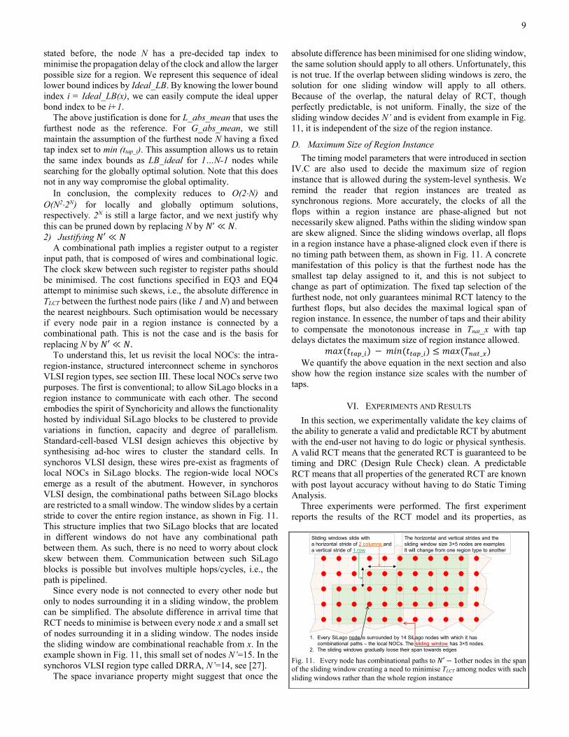
replacing N by 𝑁′ ≪ 𝑁. To understand this, let us revisit the local NOCs: the intra-
region-instance, structured interconnect scheme in synchoros
VLSI region types, see section III. These local NOCs serve two
purposes. The first is conventional; to allow SiLago blocks in a
region instance to communicate with each other. The second
embodies the spirit of Synchoricity and allows the functionality
hosted by individual SiLago blocks to be clustered to provide
variations in function, capacity and degree of parallelism.
Standard-cell-based VLSI design achieves this objective by
synthesising ad-hoc wires to cluster the standard cells. In
synchoros VLSI design, these wires pre-exist as fragments of
local NOCs in SiLago blocks. The region-wide local NOCs
emerge as a result of the abutment. However, in synchoros
VLSI design, the combinational paths between SiLago blocks
are restricted to a small window. The window slides by a certain
stride to cover the entire region instance, as shown in Fig. 11.
This structure implies that two SiLago blocks that are located
in different windows do not have any combinational path
between them. As such, there is no need to worry about clock
skew between them. Communication between such SiLago
blocks is possible but involves multiple hops/cycles, i.e., the
path is pipelined.
Since every node is not connected to every other node but
only to nodes surrounding it in a sliding window, the problem
can be simplified. The absolute difference in arrival time that
RCT needs to minimise is between every node x and a small set
of nodes surrounding it in a sliding window. The nodes inside
the sliding window are combinational reachable from x. In the
example shown in Fig. 11, this small set of nodes N’=15. In the
synchoros VLSI region type called DRRA, N’=14, see [27].
The space invariance property might suggest that once the
absolute difference has been minimised for one sliding window,
the same solution should apply to all others. Unfortunately, this
is not true. If the overlap between sliding windows is zero, the
solution for one sliding window will apply to all others.
Because of the overlap, the natural delay of RCT, though
perfectly predictable, is not uniform. Finally, the size of the
sliding window decides N’ and is evident from example in Fig.
11, it is independent of the size of the region instance.
D. Maximum Size of Region Instance
The timing model parameters that were introduced in section
IV.C are also used to decide the maximum size of region
instance that is allowed during the system-level synthesis. We
remind the reader that region instances are treated as
synchronous regions. More accurately, the clocks of all the
flops within a region instance are phase-aligned but not
necessarily skew aligned. Paths within the sliding window span
are skew aligned. Since the sliding windows overlap, all flops
in a region instance have a phase-aligned clock even if there is
no timing path between them, as shown in Fig. 11. A concrete
manifestation of this policy is that the furthest node has the
smallest tap delay assigned to it, and this is not subject to
change as part of optimization. The fixed tap selection of the
furthest node, not only guarantees minimal RCT latency to the
furthest flops, but also decides the maximal logical span of
region instance. In essence, the number of taps and their ability
to compensate the monotonous increase in Tnat_x with tap
delays dictates the maximum size of region instance allowed.
𝑚𝑎𝑥(𝑡𝑡𝑎𝑝_𝑖) − 𝑚𝑖𝑛(𝑡𝑡𝑎𝑝_𝑖) ≤ 𝑚𝑎𝑥(𝑇𝑛𝑎𝑡_𝑥)
We quantify the above equation in the next section and also
show how the region instance size scales with the number of
taps.
VI. EXPERIMENTS AND RESULTS
In this section, we experimentally validate the key claims of
the ability to generate a valid and predictable RCT by abutment
with the end-user not having to do logic or physical synthesis.
A valid RCT means that the generated RCT is guaranteed to be
timing and DRC (Design Rule Check) clean. A predictable
RCT means that all properties of the generated RCT are known
with post layout accuracy without having to do Static Timing
Analysis.
Three experiments were performed. The first experiment
reports the results of the RCT model and its properties, as
Fig. 11. Every node has combinational paths to 𝑁′ − 1other nodes in the span of the sliding window creating a need to minimise TLCT among nodes with such
sliding windows rather than the whole region instance
Sliding windows slide with
a horizontal stride of 2 columns and
a vertical stride of 1 row
The horizontal and vertical strides and the
sliding window size 3×5 nodes are examples
It will change from one region type to another
1. Every SiLago node is surrounded by 14 SiLago nodes with which it has
combinational paths – the local NOCs. The sliding window has 3×5 nodes.
2. The sliding windows gradually loose their span towards edges

10
discussed in the section IV.D. The second experiment then uses
the RCT model to predict the properties of the RCT in an
experimental design. The predicted values are validated against
the values analysed by commercial EDA tools. A side effect of
this experiment is that RCT generated by abutment is shown to
be timing and DRC clean by the commercial EDA tools. The
third experiment benchmarks the properties of RCT generated
by abutment against a functionally equivalent RCT, generated
by the EDA tools. The results of the experiment are used to
prove that the two clock trees are comparable in their figures of
merits. That is to say that the synchoricity and abutment does
not degrade the quality of the generated RCT.
A. Experimental setup
In this sub-section, we present the experimental setup we
have used for our experiments.
1) Technology and Tools
All experiments have been implemented in 40 nm technology
node and the results have been validated using commercial
EDA tools. These tools have been used for three purposes:
a) To build the synchoros VLSI design platform, including
RCT design and its characterisation. This use of EDA tools
is a one-time engineering effort, and it is not seen by the
end-user.
b) To validate the claim that the generated RCT is timing and
DRC clean and predictable.
c) To demonstrate that the benefits of synchoricity and
abutment do not degrade the quality of RCT.
2) Experimental Design
The proposed RCT by abutment scheme and the state-of-the-
art hierarchical EDA flow are applied to the same experimental
design. The design is a composite region instance of two
different types. The two types are a dense linear algebra CGRA
fabric called Dynamically Reconfigurable Resource Array
(DRRA) [20] and a CGRA for scratchpad fabric called
Distributed Memory Architecture (DiMArch) [22].
The region instance has 24 SiLago blocks that correspond to
roughly 1.5 million NAND gates and 16 kBs of SRAM, or 4
mm2 in 40 nm. The size of the design is compatible with the
expected typical size of synchronous region instance, for which
the RCT is generated by abutment. To establish the scalability
of the method, we also show the results of a 5 million gate
design and show that the predictability is unaffected.
B. RCT Model
An RCT fragment, shown in Fig. 6, with 32 taps in delay line
was incorporated into the DRRA and DiMArch SiLago blocks.
These blocks were hardened to be synchoros, and all
interconnects, including the RCT interconnects, were brought
to the periphery to enable abutment, conceptually shown in Fig.
12. The RCT model parameters were extracted using STA
(Static Timing Analysis) from the post layout data and results
tabulated in Table II. The SiLago blocks on the edges have
slightly different values of TRCT_chord compared to the ones in the
middle. Because there are minor differences in the interconnect
and the layout of the three rows in Fig. 12, each row has
different TRCT_chord delays. The delay model takes that into
consideration to correctly predict the Tnat. Here we report the
values for the middle row. The slew at LCT entry point and the
total capacitance of the RCT structure in each SiLago block is
reported as well. The tap delay ttap_i in our setup can introduce
delay from 1.7 to 6.2 ns.
The timing model created above factors in variations in
temperature, VDD and process as part of standard logic
synthesis. For the experiments reported in this paper, the timing
model takes into account the Best and the Worst Case
Commercial variations. The multi-corner analysis ensures that
the RCT constructs, along with its timing and electrical
properties, will have the robustness that has been factored in
these variations.
TABLE II
RCT MODEL’S PARAMETER VALUES
Parameter Value Parameter Value
TRCT_chord TH_to_H 0.469ns
0.48ns
TV_to_H 0.617ns
0.663ns
TH_to_V 0.47ns
0.463ns
TV_to_V 0.618ns
0.646ns
Slew at LCT entry 67ps
C. Predictability and validity
The RCT model quantified in the previous sub-section was
used to predict the properties of the RCT created by abutment,
as shown in Fig. 12. The prediction is done by taking the post
layout SiLago region instance created by abutment and
analysing the properties of the generated RCT by two methods,
as shown in Fig. 13. The first method is to use the RCT model
and SiLago analysis scripts embodied by equations 1 and 2. The
second method is to use EDA analysis tools. The results of these
paths are compared to establish the accuracy of the RCT model
with EDA tools as the benchmark. A side-effect of this
experiment is that the RCT created by abutment gets certified
as being timing and DRC clean by the EDA analysis tools.
The two RCT properties that we focus on predicting are the
arrival times of RCT, TLCT_x,i , and the slew rate at the entry
point of LCT in each of the 24 SiLago blocks. A third property
we predict is the combined capacitance of the RCT structure in
24 blocks. The optimisation algorithm described in section V.C
was used to find the optimal set of tap indices in the 24 blocks
Fig. 12. Experimental Region Instance used in Experiments.
Fig. 13. Experiment to prove predictability and validity of RCT created by
abutment.
RCT Entry
Point
DRRA
0|1
0|1
DL
DiMArch
0|1
0|1
DL
DRRA
0|1
0|1
DL
DiMArch
0|1
0|1
DL
DRRA
0|1
0|1
DL
DiMArch
0|1
0|1
DL
DRRA
0|1
0|1
DL
DiMArch
0|1
0|1
DL
DRRA
0|1
0|1
DL
DiMArch
0|1
0|1
DL
DRRA
0|1
0|1
DL
DiMArch
0|1
0|1
DL
DRRA
0|1
0|1
DL
DiMArch
0|1
0|1
DL
DRRA
0|1
0|1
DL
DiMArch
0|1
0|1
DL
DRRA
0|1
0|1
DL
DRRA
0|1
0|1
DL
DRRA
0|1
0|1
DL
DRRA
0|1
0|1
DL
DRRA
0|1
0|1
DL
DRRA
0|1
0|1
DL
DRRA
0|1
0|1
DL
DRRA
0|1
0|1
DL
DPU
Register
File
Switch
Sequ
en
cer
SRAM
2KB
Bank
Switch
Region Instance
GDSII
Created by abutment+
HLS, ALS, SLS
Output
Synchoros SiLago VLSI Design Platform1. Synchoros SiLago Blocks including RCT
fragments and other inter-SiLago wires
2. Characterized with post-layout data – RCT Timing
Model
3. Composition by abutment scripts
4. Analysis scriptsSiLago
Analysis
Scripts
EDA
Analysis
Tools
Comparison:
Valid Design
Accurate Prediction
Not part of SiLago Design Flow
Done and shown here as a proof of claims

11
to minimise the absolute difference among TLCT_x,i. Two critical
quantified conclusions can be drawn. The first is that the worst-
case absolute difference is 129 ps which is easily absorbed by
the slack margin with which the SiLago blocks are synthesised.
The second is that the predicted values by the SiLago Analysis
Tools are almost identical to the one analysed by the EDA tools.
The worst-case error compared to EDA tools is 1.5 ps, and the
RMS is 0.0005ps. We believe that this difference comes from
the fact that our experimental setup does not have an infinite
ground plane. This results in different parts of the design
experiencing different coupling with long signals, like the reset,
and the ground plane. The resulting model suffices as a proof
of concept and provides sufficient accuracy that a post abutment
STA is not needed.
The slew rate at each LCT entry point and the total
capacitance predicted by both methods are a near-perfect match
between SiLago and EDA tools. The SiLago design reports
slew and capacitance equal to 67ps and 129.9pf. The EDA
respective values are 87ps and 127.2pf. We want to note here
that this is the capacitance for the whole clock in the region
composed of RCT and LCT. LCT dominates the percentage
capacitance with 97% capacitance, while the RCT has just 3%.
To address scalability concerns, we first performed the
experiments, as reported above, using a baseline design of eight
columns and three rows. The baseline design corresponds to
~1.5 million gate. Then we repeated the experiment for a larger
design with twenty-five columns and three rows corresponding
to roughly 5 million gates. The predictability of the larger
design was as good as the one of the smaller design.
D. SiLago RCT comparison with EDA
In this section, we demonstrate that the quality of RCT
(Regional Clock Tree) generated by abutment is comparable to
a functionally equivalent RCT generated as part of a
hierarchical EDA flow. This experiment is visualized in Fig. 14.
The Synchoros SiLago design flow starts with an untimed
model at application/system-level. Application/System-level
synthesis then transforms the model into a logical netlist of
SiLago blocks – the region-instance; in the current context, a
single region instance1 shown in Fig. 12. The SiLago blocks in
the netlist are picked from the Synchoros SiLago VLSI design
platform. The VLSI design, including RCT, of the region
instance, is created by abutment. Note that the creation of the
1 In general, ALS and SLS will output multiple region-instances connected by global NOCs and communicate on latency insensitive basis using GRLS [25].
synchoros VLSI design platform is a one-time engineering
effort, like the standard cell library creation.
The second path is based on commercial hierarchical EDA
flow. It starts with a logical netlist of RTL SiLago blocks that
do not include the regional (inter-SiLago block) wires like
RCT. SiLago blocks are hardened but do not include global
wires. Once hardened, these blocks are floor-planned and the
regional clock tree and inter-SiLago block wire have to be
synthesized. This is done with the physical synthesis step that
follows the floorplanning and generates the functionally
equivalent RCT tree. Note that in EDA terminology, the RCT
and inter-SiLago block wires are called global wires. We refrain
from using the term global to maintain consistency with the
SiLago flow, where global implies inter-region instance wires.
Both designs are then analysed by the commercial EDA tools
to compare the properties of the two functionally equivalent
RCTs. The results are shown in Table III. As can be seen, the
values of critical parameters are comparable. The standard cell
area refers to standard cells dedicated to creation of RCT,
including MUX/AND/OR gates as reported from the EDA
tools. In SiLago case, each SiLago block has a fixed overhead,
and not all of it is used. This is the key reason for a larger
overhead compared to the EDA RCT. However, do note that the
RCT area as a percentage of SiLago block takes up only 0.1%.
The SiLago RCT achieves comparable arrival time of RCT
at LCT (Local Clock Tree) entry points compared to the
commercial EDA RCT. The SiLago RCT has slightly better
slew rate at LCT entry. The average and absolute difference in
slew at different points in trunks for the entire (RCT+LCT)
clock tree is also comparable and within the limits of the
technology rules.
TABLE III
EDA RCT VS SILAGO RCT
SiLago RCT EDA RCT
Wire Length 422932.1 μm 415263.9 μm
Standard Cell Area 19472.6 μm2 18276.5 μm2
Average Trunk Slew 0.062 ns 0.090 ns
Total Capacitance 129.9pf 127.2 pf
Avg. Diff. in Arrival Time (LCT Entry Point) 0.04299ns 0.0337 ns
The above experiment and the reported results establishes
that RCT generated by abutment has comparable quality as the
one generated by commercial EDA tools. The difference is that
the EDA tool generated RCT is ad-hoc and synthesised anew
for each design instance. Notice that the EDA RCT’s
irregularity in Fig. 15a resulting from the attempt to factor and
reuse the buffers. In contrast, the synchoros RCT is regular. The
ad-hoc nature of the EDA RCT and its irregularity violates the
requirements that synchoros VLSI design places on RCT.
The synchoros RCT by abutment is regular, as shown in Fig.
15b. It has three main branches corresponding to two DRRA
and one DiMArch rows. Each branch has eight leaf nodes, and
each leaf node has the same RCT structure. The regularity of
the SiLago RCT enables abutment. Its regular structure,
together with its absorption in the SiLago blocks as a pre-
synthesized and characterised structure, enables predictability.
Though not the most critical difference, the RCT generated
by commercial EDA tools took ~50 minutes for synthesis and
In this paper and experiment, we focus on RCT generation by abutment in a single region instance. The same process would apply to all region-instances.
Fig. 14. VLSI of Region Instance created by Synchoros and commercial EDA
flows
Block
Hardening
Floor
planning
RCT
synthesis
Global
Routing
STA &
DRC
Verification
RTL of SiLago
Block and Region
Instance
Region Instance
GDSII
Created by abutment+
Netlist of SiLago Blocks
Output of ALS/SLS
Synchoros SiLago VLSI Design Platform1. Synchoros SiLago Blocks including RCT fragments and other inter-
SiLago wires
2. Characterized with post-layout data – RCT Timing Model
3. Composition by abutment scripts
4. Analysis scripts
STA &
DRC
Verification
EDA RTC
Quality
SiLago
RTC
Quality
Logic and Physical Syntheses of SiLago Blocks
including synthesis of LCT but not RCT or other
regional wires

12
another ~5 minutes for STA, for a modest 1.5 million gate
design. Any post-CTS optimisation requires another ~30min.
This time is expected to increase exponentially with design size.
In the case of synchoros RCT, the clock tree generation and its
analysis are instantaneous.
VII. STATE OF THE ART
In this section, we justify the contributions of this paper in
comparison to the state-of-the-art, primarily in clock tree
synthesis but also in composition by abutment.
CTS (Clock Tree Synthesis) has been researched since the
earliest days of VLSI. One of the most critical chapters in the
classic textbook on VLSI Systems by Mead-Conway [14] is
dedicated to clocking and timing. Ever since then, CTS has
been a mainstream VLSI research topic. The main objective of
CTS research has been to optimise the cost metrics of the clock
tree, i.e., smaller switching capacitance, minimising skew,
maintaining edge etc. [28, 29]. These approaches are based on
sophisticated heuristic algorithms. Most of these methods are
based on the van Ginneken dynamic programming algorithm
for buffer insertion and sizing, and the delay model used is the
Elmore delay model [30]. An excellent survey of CTS
techniques is presented in [31]. Additionally, they propose their
own algorithm for chip-level clock tree synthesis that
minimises the skew and is manufacturing variation aware. [32,
33] also propose solutions to chip-level clock tree synthesis that
is aware of on-chip variations. J. Lu et al. in [34] address a
different problem with a similar method, where they use a post-
clock-tree-synthesis optimisation to improve the clock period.
The proposed method addresses the problem by buffering an
already synthesized clock tree. They are considering the
synthesised local clock tree and the delay of the logic path,
allowing for non-zero skew. In contrast, our goal is not to
optimise the clock period, but to balance the arrival time of the
clock at the source points of the local clock trees. The balance
of the RCT is done by configuring an existing delay line that
has already been implemented. In synchoros VLSI design style,
once a SiLago block has been designed, no further change is
possible and no additional external circuitry can be added.
With dynamic voltage frequency scaling becoming
mainstream, research in clock tree also addressed concerns
raised by varying VDD. Any variation in VDD changes the
drive and thus influences the amount of skew. A common
method to address this problem is the use of Adjustable Delay
Buffers (ADBs). There have been many research work recently
that addresses this problem using ADBs [35 - 37].
H-tree and Mesh clock structures have also been widely
researched [30, 38]. The regularity of these structures makes
them a good match for the synchoros VLSI design style.
However, both these structures do not fulfil the requirements
that RCT by abutment has as part of synchoros VLSI design
style. H-Tree is a hierarchical structure, and its depth would
depend on the size of the region instance. For this reason,
absorbing an H-Tree as RCT fragments and being able to create
an arbitrary H-Tree by abutment that is depended on the size
and shape of region instance is not feasible. Mesh-based clock
tree poses a challenge in terms of the predictability requirement.
Since the entry point in clock tree mesh, an equipotential
surface, is not known, it creates cyclic graphs that are
impossible to analyse with STA [30, 38]. This is an even bigger
problem for the RCT by abutment scheme because it requires
no STA. Because of that, it is required to have iron-clad timing
models that can predict the properties of RCT with sufficient
accuracy. However, we note that in terms of geometry, the
proposed RCT structure is a mesh structure, in which the entry
point and propagation of RCT is known. The standardised entry
points and propagation path makes it analysable and possible to
create the RCT model, as shown in section IV.D. .
FPGAs, like synchoros VLSI designs, are regular structures
and naturally invite comparison of their clock tree schemes. The
fundamental difference in regularity is that the regularity of
FPGAs is not modifiable in silicon for the end user. In other
words, no matter how the end user configures an FPGA, the
clock tree wires will not change in their position, length or
drive. These wires can be configured differently but the silicon
will not change. In contrast, depending on functionality and
constraints, the output of application and system-level synthesis
will imply different RCT wires in silicon. All of the wires are
regular and structured but connected in such a way to produce
different structures. FPGAs partition their leaf nodes – the flops
– into clusters based on spatial locality. These clusters can be
clocked by different global clock tree wires in a configurable
manner. Further, depending on the datapath created by the end-
user and the choice of the clock to drive them, FPGAs do
require an STA as a post-synthesis step. In synchoros VLSI
design, unlike FPGAs, the datapath is highly customised for a
specific application domain – much more than DSP slices in
FPGAs. These regions are pre-characterized to work at certain
clock speeds, as long as RCT infrastructure can deliver RCT to
the LCT entry points within a known skew margin. This is the
reason why in synchoros VLSI design, no STA is required as a
follow-up step and region instances of arbitrary size that are
hosting arbitrary domain-specific functionality are guaranteed
to be correct-by-construction.
The clock tree synthesis research that we address in this
paper does not compete directly with these approaches. The
method reported in this paper complements and builds on
Fig. 15. The ad-hoc unstructured EDA RCT vs the regular structured
synchoros SiLago RCT
(a) EDA Regional Clock Tree
LCT
Clock Buffer
(b) SiLago Regional Clock Tree
Delay Line
Clock Gate
Clock Mux
LCT

13
existing research. As shown by our experiments and would be
evident to most practitioners of VLSI design, LCT has the
dominant switching capacitance. For that reason, we rely on the
existing body of research to automate this step. What we
propose is an alternative to the clock tree generation at a higher
level, which has relatively insignificant capacitance but
profoundly affects the engineering cost.
The proposed solution most directly competes against the
widely prevalent hierarchical synthesis flow of the EDA tools
and their global clock tree synthesis phase. We propose to
replace this ad-hoc follow-up synthesis step with a one-time
engineering effort. That makes the generation of VLSI design
alternatives non-incrementally faster, easier and most critically
predictable and correct by construction. We believe this is
essential to automate the higher abstraction synthesis (see Fig.
1) as argued by Hemani et al. in [1].
Besides the RCT synthesis, another aspect of research that is
proposed in this paper is the composition by abutment. Once
again, this method is also as old as the VLSI designs. The Mead-
Conway [14] method involved composing macros by abutting
bit slices. Later, these macros were parametrised, and complete
system-level design was attempted as part of silicon compiler
research. This phase of VLSI design automation was eclipsed
when standard cells were introduced, and composition by
abutment as a method lost its appeal. More recently, [39, 40]
have proposed methods that bear some similarity to the SiLago
method. The proposed method does not detail how they propose
to handle the synthesis of infrastructural wires like clocks,
resets and power grid by abutment. The critical difference that
the SiLago method has is that it aims at automating the
synthesis of functional hardware. Whereas, [39, 40] aim at
incrementally improving the EDA tool’s hierarchical synthesis
flow for designing processor centric infrastructural hardware.
VIII. CONCLUSION AND FUTURE WORK
We have presented a regional clock tree synthesis method
based on abutting identical fragments of the clock tree. The
fragments are absorbed in the one-time VLSI engineered
abuttable SiLago blocks. The generated clock tree is shown to
be valid, i.e. timing clean, comparable in its cost metrics to a
functionally equivalent clock tree generated by the EDA tools.
The advantage that the proposed scheme has over the
conventional EDA based method is that it generates a
predictable and correct by construction design of the regional
clock tree. Besides that, the proposed method does not require
a clock tree synthesis step for the generation of the RCT. We
argue that this is essential to enable automation of functional
hardware from higher abstractions. We have shown that the
scheme is scalable to larger designs of ~5 million gate
complexity and the synthesis time required is less than a minute.
The programmable delay line is constructed from qualified
standard cells, and its atomic delay decides the resolution to
which we can minimise the skew. We are working on a more
advanced programmable delay line that will allow a finer
adjustment of delay that would be needed for higher
frequencies. In this improved delay line, the number of taps
would increase logarithmically with the amount of delay.
Thereby the size of design over which it can maintain
synchronicity would be increased. Such a delay line will be
constructed with weighted positional taps much like a fixed-
point number. We are also in the process of making the delay
of each tap in the delay line adaptive. That will allow it to be
adjusted in response to changes in Vdd as part of dynamic
voltage frequency scaling scheme.
ACKNOWLEDGEMENT
This work is supported by Vinnova, Sweden as part of the
CREST II project.
REFERENCES
[1] A Hemani, S.M.A.H Jafri, S Masoumian, “Synchoricity and NOCs could make Billion Gate Custom Hardware Centric SOCs Affordable,” International Symposium NOCS, 2017.
[2] W. J. Dally, et al., “Efficient embedded computing,” Computer, vol. 41, 2008.
[3] J. Rabaey, “Silicon Platforms for the Next-Generation Wireless Systems.” Tutorial in HotChips 13, 2001.
[4] E. S. Chung, et al., “Single-chip heterogeneous computing: Does the future include custom logic, FPGAs, and GPGPUs?,” in MICRO 2010.
[5] M. Khazraee, L. V. Gutierrez, I. Magaki, and M. B. Taylor, “Specializing a Planet’s Computation: ASIC Clouds,” IEEE Micro, vol. 37, no. 3, 2017.
[6] N. P. Jouppi, et al., “In - Datacenter Performance Analysis of a Tensor Processing Unit,” in Proceedings of ISCA ’17, 2017.
[7] S. Hanley, “Autonomous Cars Have Shorter Range Due To High Power Consumption By Computers,” CleanTechnica, 13-Oct-2017.
[8] K. Freund, “Will ASIC Chips Become The Next Big Thing In AI?,” Forbes, 04-Aug-2017.
[9] S. M. A. H. Jafri, A. Hemani, K. Paul, and N. Abbas, “MOCHA: Morphable Locality and Compression Aware Architecture for Convolutional Neural Networks,” in Proceedings of the IPDPS, 2017.
[10] Y. H. Chen, et al., “Eyeriss: A Spatial Architecture for Energy-Efficient Dataflow for Convolutional Neural Networks,” ISCA 2016.
[11] Y. Yang, et al., “RiBoSOM : Rapid Bacterial Genome Identification Using Self-Organizing Map implemented on the Synchoros SiLago Platform,” in Proceedings of the SAMOS, 2018.
[12] R. Merritt, “FPGAs add comms cores amid ASIC debate,” EE Times, 03-Nov-2013.
[13] D. Stathis, et al. “eBrainII: A 3 kW Realtime Custom 3D DRAM integrated ASIC implementation of a Biologically Plausible Model of a Human Scale Cortex.” arXiv preprint arXiv:1911.00889 (2019).
[14] Carver A Mead, Lynn A Conway, “Introduction To VLSI Systems”, Addision-Wesley. ISBN-13: 978-0201043587.
[15] B. Bailey, “ESL Flow Is Dead,” Semiconductor Engineering, April 28, 2016.
[16] S. Li, N. Farahini, A. Hemani, K. Rosvall, I. Sander, “System Level Synthesis of Hardware for DSP Applications Using Pre-Characterized Function Implementations,” Proceedings of the ISSS Codes 2013.
[17] A. Krste, et al., “The Landscape of Parallel Computing Research: A View from Berkeley,” EECS Department, UC, Berkeley, 2006.
[18] T. Miyamori and K. Olukotun, “Remarc: Reconfigurable multimedia array coprocessor,” IEICE Trans. Inf. Syst., vol. E82–D, no. 2, 1998.
[19] P. M. Heysters, G. J. M. Smit, and E. Molenkamp, “Energy-efficiency of the Montium reconfigurable tile processor.,” in Proceedings of the ERSA ’04, 2004.
[20] M. A. Shami and A. Hemani, “Control scheme for a CGRA,” Proceedings of the SBAC-PAD, 2010.
[21] M. A. Shami and A. Hemani, “Address generation scheme for a coarse grain reconfigurable architecture,” in Proceedings of the ASAP, 2011.
[22] M. A. Tajammul, M. A. Shami, A. Hemani, and S. Moorthi, “A NoC based distributed memory architecture with programmable and partitionable capabilities,” in 28th Norchip Conference, 2010.
[23] P. Liu, F. O. Ebrahim, A. Hemani, and K. Paul, “A coarse-grained reconfigurable processor for sequencing and phylogenetic algorithms in bioinformatics,” in Proceedings - ReConFig 2011.

14
[24] M. Badawi, Z. Lu, and A. Hemani, “Service-Guaranteed Multi-port Packet Memory for Parallel Protocol Processing Architecture,” in Proceedings - 24th Euromicro International Conference PDP 2016.
[25] J.-M. Chabloz and A. Hemani, A., "Low-Latency Maximal-Throughput Communication Interfaces for Rationally Related Clock Domains," IEEE TVLSI , vol.22, no.3, pp.641,654, March 2014.
[26] S. M. A. H. Jafri, N. Farahini and A. Hemani, “SiLago-CoG: Coarse-Grained Grid-Based Design for Near Tape-Out Power Estimation Accuracy at High Level,” 2017 ISVLSI, Bochum, 2017.
[27] M. A. Shami and A. Hemani, “Partially reconfigurable interconnection network for dynamically reprogrammable resource array,” Proceedings 2009 8th IEEE International Conference on ASIC, 2009.
[28] T. H. Chao, et al., “Zero Skew Clock Routing with Minimum Wirelength,” IEEE Trans. Circuits Syst. II Analog Digit. Signal Process., vol. 39, no. 11, 1992.
[29] P. J. Restle et al., “A clock distribution network for microprocessors,” in 2000 Symposium on VLSI Circuits Digest of Technical Papers, 2000.
[30] L. Lavagno, I. L. Markov, G. Martin, and L. K. Scheffer, “Clock Design and Synthesis” in Electronic Design Automation for IC Implementation, Circuit Design, and Process Technology, CRC Press, US.
[31] A. Rajaram, and D. Z. Pan, “Robust Chip-Level Clock Tree Synthesis”, IEEE TCAD, June 2011.
[32] T. J. Wang, S. H. Huang, W. K. Cheng, and Y. C. Chou, “Top-level activity-driven clock tree synthesis with clock skew variation considered,” in Proceedings - IEEE International Symposium on Circuits and Systems, 2016.
[33] C. Deng, Y. Cai, and Q. Zhou, “Fast synthesis of low power clock trees based on register clustering,” in Proceedings - International Symposium on Quality Electronic Design, ISQED, 2015.
[34] J. Lu and B. Taskin, “Post-CTS clock skew scheduling with limited delay buffering,” in Midwest Symposium on Circuits and Systems, 2009.
[35] J. Kim, and T. Kim, “Adjustable Delay Buffer Allocation under Useful Clock Skew Scheduling”, IEEE TCAD Vol 36, No 4, April 2017.
[36] K. Park, G. Kim, and T. Kim, “Mixed Allocation of Adjustable Delay Buffers Combined with Buffer Sizing in Clock Tree Synthesis of Multiple Power Mode Designs”, vol. 1. European Design and Automation Association, 2014.
[37] C.-C. Kao, “Clock Skew Minimization in Multiple Dynamic Supply Voltage with Adjustable Delay Buffers Restriction,” J. Signal Process. Syst., vol. 79, no. 1, Apr. 2015.
[38] A. Abdelhadi, et. al. “Timing–Driven Variation–Aware Nonuniform Clock Mesh Synthesis,” in Proceedings of the 20th symposium on Great lakes symposium on VLSI, 2010.
[39] W. J. Dally, C. Malachowsky, S. W. Keckler, “21st Century Digital Design Tools”. DAC 2013.
[40] R. Merritt, “EE Slashes CPU Design Cost: 4.5B transistor tapeout for less than $1M,” EE Times, 10-May-2016.
Dimitrios Stathis received his Diploma in
Electr. & Comp. Engineering and a M.Sc. in
Microelectronics and Computer Systems,
both from the Democritus University of
Thrace, Xanthi, Greece in 2013 and 2016
respectively. He received his second M.Sc.
degree in Embedded Systems from KTH,
Stockholm, Sweden in 2017. He is currently working towards
the PhD degree at the KTH, Stockholm, Sweden. His research
interests include Computer Architectures and ASIC design for
multimedia applications and Artificial Neural Networks.
Panagiotis Chaourani received the B.Sc.
degree in Physics and the M.Sc. degree in
Electronics, both from the Aristotle
University of Thessaloniki, Thessaloniki,
Greece in 2011 and 2014 respectively. He is
currently working towards the PhD degree
at the KTH, Stockholm, Sweden. His
research interests include IC design, CAD tools and monolithic
3-D integration.
Dr. Syed M. A. H. Jafri is a senior system
architect working at Ericsson. Before that,
he worked as a post-doc researcher at the
Royal Institute of Technology (KTH). He
received his B.Sc. degree in 2005 from
National University of Sciences and
Technology in Rawalpindi, Pakistan. From
2005 to 2007 he was with Siemens, Pakistan. In 2009 he
received MSc in system on chip design from Royal Institute of
Technology (KTH), Sweden. He did PhD from University of
Turku, Finland in 2015. He has 40+ peer-reviewed
journals/conference publications.
Ahmed Hemani is Professor in the
Electronics Dept. at School of EECS,
KTH, Stockholm, Sweden since 2006. His
doctoral thesis on HLS was the basis for
one of the first commercial HLS product
from CADENCE. Later he has contributed
to latency insensitive design style with
research on GALS and GRLS. He also pioneered the concept of
NOCs. His current research interests focus on massively
parallel architecture and design methods for them to achieve
ASIC comparable performance. He has introduced the concept
of synchoricity and driven the development of the SiLago as an
experimental synchoros VLSI design platform. He is applying
synchoros VLSI design to artificial neural networks,
biologically plausible models of brain and complex multi-
media and telecom applications.