Reference Design for Extending OPA857 … · important notice for ti reference designs
14
+ – RF1 RF2 TIA IN REF CLAMPING CIRCUIT 25 25 OUT OUTN CLAMP 1:1 2 k TEST Test_In Test_SD CTRL +VS GND External RF VBIAS External CF Copyright © 2016, Texas Instruments Incorporated 1 TIDUBX71 – April 2016 Submit Documentation Feedback Copyright © 2016, Texas Instruments Incorporated Reference Design for Extending OPA857 Transimpedance Bandwidth TI Designs Reference Design for Extending OPA857 Transimpedance Bandwidth TINA-TI is a trademark of Texas Instruments. Excel is a registered trademark of Microsoft Corporation. All other trademarks are the property of their respective owners. TI Designs The OPA857 is a wideband, ultra-low noise transimpedance amplifier (TIA) that supports photodiode monitoring applications. The OPA857 has two selectable gain configurations of 5 kΩ and 20 kΩ while maintaining a constant closed-loop bandwidth greater than 100 MHz. In this reference design, an external resistor is added in parallel with the internal gain resistor of the OPA857 to extend the transimpedance bandwidth of the amplifier. Design Resources TIDA-00978 Design Folder OPA857 Product Folder TINA-TI™ Tools Folder ASK Our E2E Experts Design Features • Bandwidth of OPA857 Extended From 100 MHz to More Than 250MHz • Gain of OPA857 Adjustable Between 1 kΩ and 20 kΩ • Evaluation Module (EVM) Facilitates Testing OPA857 in Internal-Test Mode or With External Photodiode Featured Applications • Optical Amplifiers • LIDAR • OTDR • Photodiode Monitoring • Machine Vision • Missile Guidance An IMPORTANT NOTICE at the end of this TI reference design addresses authorized use, intellectual property matters and other important disclaimers and information.
-
Upload
phungthuan -
Category
Documents
-
view
227 -
download
0
Transcript of Reference Design for Extending OPA857 … · important notice for ti reference designs
+
±
RF1
RF2
TIA
IN
REFCLAMPING
CIRCUIT
25
25
OUT
OUTN
CLAMP
1:12 k
TEST
Test_In
Test_SD
CTRL +VS GND
External RF
VBIAS
External CF
Copyright © 2016, Texas Instruments Incorporated
1TIDUBX71–April 2016Submit Documentation Feedback
Copyright © 2016, Texas Instruments Incorporated
Reference Design for Extending OPA857 Transimpedance Bandwidth
TI DesignsReference Design for Extending OPA857 TransimpedanceBandwidth
TINA-TI is a trademark of Texas Instruments.Excel is a registered trademark of Microsoft Corporation.All other trademarks are the property of their respective owners.
TI DesignsThe OPA857 is a wideband, ultra-low noisetransimpedance amplifier (TIA) that supportsphotodiode monitoring applications. The OPA857 hastwo selectable gain configurations of 5 kΩ and 20 kΩwhile maintaining a constant closed-loop bandwidthgreater than 100 MHz. In this reference design, anexternal resistor is added in parallel with the internalgain resistor of the OPA857 to extend thetransimpedance bandwidth of the amplifier.
Design Resources
TIDA-00978 Design FolderOPA857 Product FolderTINA-TI™ Tools Folder
ASK Our E2E Experts
Design Features• Bandwidth of OPA857 Extended From 100 MHz to
More Than 250MHz• Gain of OPA857 Adjustable Between 1 kΩ and
20 kΩ• Evaluation Module (EVM) Facilitates Testing
OPA857 in Internal-Test Mode or With ExternalPhotodiode
Featured Applications• Optical Amplifiers• LIDAR• OTDR• Photodiode Monitoring• Machine Vision• Missile Guidance
An IMPORTANT NOTICE at the end of this TI reference design addresses authorized use, intellectual property matters and otherimportant disclaimers and information.
Key System Specifications www.ti.com
2 TIDUBX71–April 2016Submit Documentation Feedback
Copyright © 2016, Texas Instruments Incorporated
Reference Design for Extending OPA857 Transimpedance Bandwidth
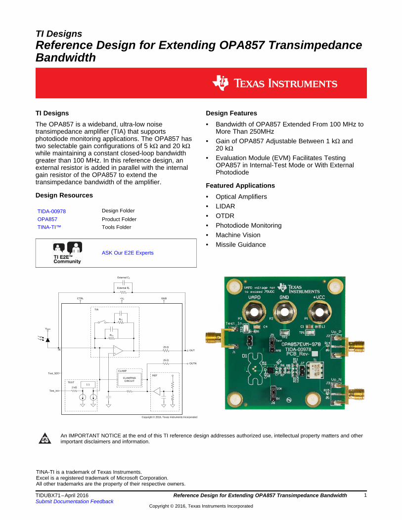
1 Key System Specifications
Table 1. Key System Specifications
PARAMETER SPECIFICATIONSSupply Voltage 3.3 V external supplyOutput swing 500 mVPP
Differential-output Load 500 Ω and 1 kΩTarget bandwidth > 250 MHzEffective transimpedance-gain range 2 kΩ to 20 kΩ
2 System DescriptionThe OPA857 described in Section 2.1 is a fixed-gain, high-bandwidth amplifier designed fortransimpedance applications. By adding an external resistor in parallel with the internal fixed-gain resistor,circuit designers can use the high-gain bandwidth product (GBP) of the internal core amplifier to achievetransimpedance bandwidths that are greater than 250 MHz at the expense of a lower closed-looptransimpedance gain.
2.1 OPA857The OPA857 provides a combination of low-noise, high-bandwidth, and high-transimpedance gain. With atargeted low input capacitance of 1.5 pF, the OPA857 achieves greater than a 100-MHz bandwidth withthe 5-kΩ or 20-kΩ transimpedance gain and adds the lowest possible RMS noise.
NOTE: The 1.5-pF capacitance includes the parasitic capacitance of the board; stray capacitancemust be minimized in the layout.
The 1.5-pF value is selected because the device should be driven by a photodiode with biasing that ishigh enough to include the capacitance of the photodiode between approximately 0.5 pF and 0.7 pF,leaving between 0.8 pF to 1 pF for the parasitic capacitance of the board.
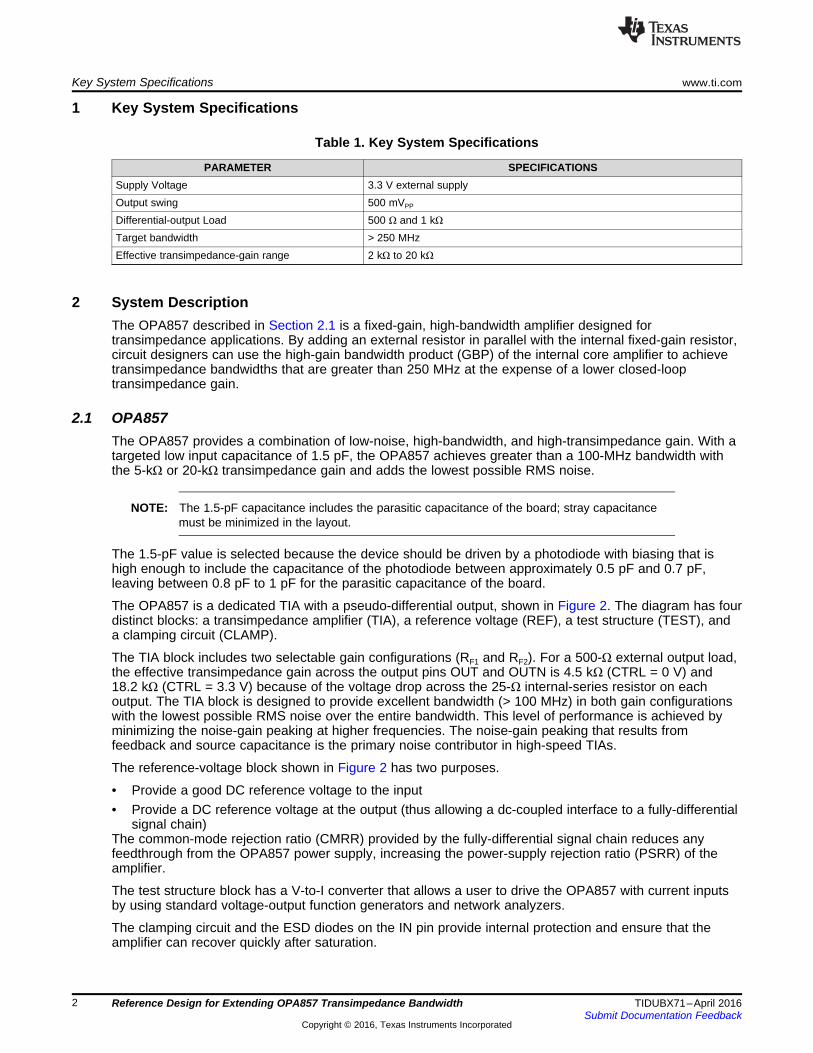
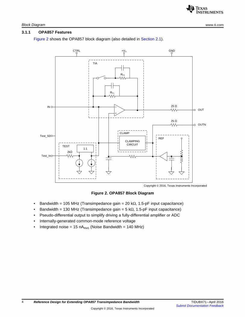
The OPA857 is a dedicated TIA with a pseudo-differential output, shown in Figure 2. The diagram has fourdistinct blocks: a transimpedance amplifier (TIA), a reference voltage (REF), a test structure (TEST), anda clamping circuit (CLAMP).
The TIA block includes two selectable gain configurations (RF1 and RF2). For a 500-Ω external output load,the effective transimpedance gain across the output pins OUT and OUTN is 4.5 kΩ (CTRL = 0 V) and18.2 kΩ (CTRL = 3.3 V) because of the voltage drop across the 25-Ω internal-series resistor on eachoutput. The TIA block is designed to provide excellent bandwidth (> 100 MHz) in both gain configurationswith the lowest possible RMS noise over the entire bandwidth. This level of performance is achieved byminimizing the noise-gain peaking at higher frequencies. The noise-gain peaking that results fromfeedback and source capacitance is the primary noise contributor in high-speed TIAs.
The reference-voltage block shown in Figure 2 has two purposes.
• Provide a good DC reference voltage to the input• Provide a DC reference voltage at the output (thus allowing a dc-coupled interface to a fully-differential
signal chain)The common-mode rejection ratio (CMRR) provided by the fully-differential signal chain reduces anyfeedthrough from the OPA857 power supply, increasing the power-supply rejection ratio (PSRR) of theamplifier.
The test structure block has a V-to-I converter that allows a user to drive the OPA857 with current inputsby using standard voltage-output function generators and network analyzers.
The clamping circuit and the ESD diodes on the IN pin provide internal protection and ensure that theamplifier can recover quickly after saturation.
+
±
RF1
RF2
TIA
IN
REFCLAMPING
CIRCUIT
25
25
OUT
OUTN
CLAMP
1:12 k
TEST
Test_In
Test_SD
CTRL +VS GND
External RF
VBIAS
External CF
Copyright © 2016, Texas Instruments Incorporated
www.ti.com Block Diagram
3TIDUBX71–April 2016Submit Documentation Feedback
Copyright © 2016, Texas Instruments Incorporated
Reference Design for Extending OPA857 Transimpedance Bandwidth
3 Block DiagramA block diagram of the system is shown in Figure 1.
Figure 1. System Block Diagram
3.1 Highlighted ProductsThis reference design features the OPA857.
For more information on the OPA857 device, see the product folder at OPA857.
+
±
RF1
RF2
TIA
IN
REFCLAMPING
CIRCUIT
25
25
OUT
OUTN
CLAMP
1:12k
TEST
Test_In
Test_SD
CTRL +VS GND
Copyright © 2016, Texas Instruments Incorporated
Block Diagram www.ti.com
4 TIDUBX71–April 2016Submit Documentation Feedback
Copyright © 2016, Texas Instruments Incorporated
Reference Design for Extending OPA857 Transimpedance Bandwidth
3.1.1 OPA857 FeaturesFigure 2 shows the OPA857 block diagram (also detailed in Section 2.1).
Figure 2. OPA857 Block Diagram
• Bandwidth = 105 MHz (Transimpedance gain = 20 kΩ, 1.5-pF input capacitance)• Bandwidth = 130 MHz (Transimpedance gain = 5 kΩ, 1.5-pF input capacitance)• Pseudo-differential output to simplify driving a fully-differential amplifier or ADC• Internally-generated common-mode reference voltage• Integrated noise = 15 nARMS (Noise Bandwidth = 140 MHz)
www.ti.com System Design Theory
5TIDUBX71–April 2016Submit Documentation Feedback
Copyright © 2016, Texas Instruments Incorporated
Reference Design for Extending OPA857 Transimpedance Bandwidth
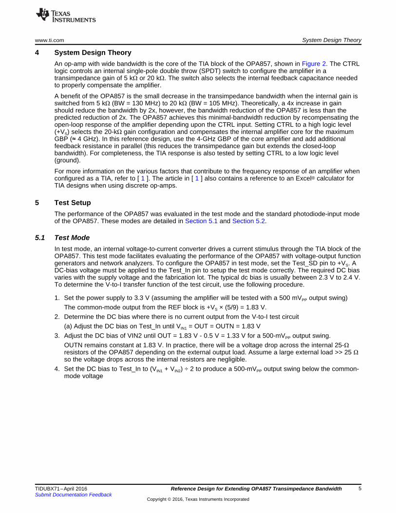
4 System Design TheoryAn op-amp with wide bandwidth is the core of the TIA block of the OPA857, shown in Figure 2. The CTRLlogic controls an internal single-pole double throw (SPDT) switch to configure the amplifier in atransimpedance gain of 5 kΩ or 20 kΩ. The switch also selects the internal feedback capacitance neededto properly compensate the amplifier.
A benefit of the OPA857 is the small decrease in the transimpedance bandwidth when the internal gain isswitched from 5 kΩ (BW = 130 MHz) to 20 kΩ (BW = 105 MHz). Theoretically, a 4x increase in gainshould reduce the bandwidth by 2x, however, the bandwidth reduction of the OPA857 is less than thepredicted reduction of 2x. The OPA857 achieves this minimal-bandwidth reduction by recompensating theopen-loop response of the amplifier depending upon the CTRL input. Setting CTRL to a high logic level(+VS) selects the 20-kΩ gain configuration and compensates the internal amplifier core for the maximumGBP (≈ 4 GHz). In this reference design, use the 4-GHz GBP of the core amplifier and add additionalfeedback resistance in parallel (this reduces the transimpedance gain but extends the closed-loopbandwidth). For completeness, the TIA response is also tested by setting CTRL to a low logic level(ground).
For more information on the various factors that contribute to the frequency response of an amplifier whenconfigured as a TIA, refer to [ 1 ]. The article in [ 1 ] also contains a reference to an Excel® calculator forTIA designs when using discrete op-amps.
5 Test SetupThe performance of the OPA857 was evaluated in the test mode and the standard photodiode-input modeof the OPA857. These modes are detailed in Section 5.1 and Section 5.2.
5.1 Test ModeIn test mode, an internal voltage-to-current converter drives a current stimulus through the TIA block of theOPA857. This test mode facilitates evaluating the performance of the OPA857 with voltage-output functiongenerators and network analyzers. To configure the OPA857 in test mode, set the Test_SD pin to +VS. ADC-bias voltage must be applied to the Test_In pin to setup the test mode correctly. The required DC biasvaries with the supply voltage and the fabrication lot. The typical dc bias is usually between 2.3 V to 2.4 V.To determine the V-to-I transfer function of the test circuit, use the following procedure.
1. Set the power supply to 3.3 V (assuming the amplifier will be tested with a 500 mVPP output swing)The common-mode output from the REF block is +VS × (5/9) = 1.83 V.
2. Determine the DC bias where there is no current output from the V-to-I test circuit(a) Adjust the DC bias on Test_In until VIN1 = OUT = OUTN = 1.83 V
3. Adjust the DC bias of VIN2 until OUT = 1.83 V - 0.5 V = 1.33 V for a 500-mVPP output swing.OUTN remains constant at 1.83 V. In practice, there will be a voltage drop across the internal 25-Ωresistors of the OPA857 depending on the external output load. Assume a large external load >> 25 Ωso the voltage drops across the internal resistors are negligible.
4. Set the DC bias to Test_In to (VIN1 + VIN2) ÷ 2 to produce a 500-mVPP output swing below the common-mode voltage
Copyright © 2016, Texas Instruments Incorporated
+
±
RF1
RF2
TIA
IN
REFCLAMPING
CIRCUIT
25
25
OUT
OUTN
CLAMP
1:12 k
TEST
Test_In
Test_SD = +VS
CTRL = +VS / GND +VS = 3.3 V
GND
CDIODE
AC = (VIN1 - VIN2)
DC = (VIN1 + VIN2) / 2
VOUT_DIFF = 500 mVPP
Test Setup www.ti.com
6 TIDUBX71–April 2016Submit Documentation Feedback
Copyright © 2016, Texas Instruments Incorporated
Reference Design for Extending OPA857 Transimpedance Bandwidth
The output stage of the OPA857 is optimized to swing below the internal common-mode reference voltage(1.83V) because photodiodes generate a unidirectional output current. The AC signal applied for a 500-mVPP output swing is equal to VIN1 - VIN2. The circuit shown in Figure 3 was used to test the frequencyresponse of the OPA857.
This procedure was also used to measure the frequency response of the OPA957.
NOTE: When evaluating the performance of the amplifier in test mode, add a physical capacitor atthe IN pin of the OPA957 to mimic the input capacitance of the target photodiode.
Figure 3. Frequency Response Test Circuit
Copyright © 2016, Texas Instruments Incorporated
+
±
RF1
RF2
TIA
IN
REFCLAMPING
CIRCUIT
25
25
OUT
OUTN
CLAMP
1:12 k
TEST
Test_In = +VS
Test_SD = GND
CTRL = +VS / GND +VS = 3.3 V
GND
Hi-Z differential scope probe
VBIAS
Optical pulse from laser
Copyright © 2016, Texas Instruments Incorporated
+
±
RF1
RF2
TIA
IN
REFCLAMPING
CIRCUIT
25
25
OUT
OUTN
CLAMP
1:12 k
TEST
Test_In = +VS
Test_SD = GND
CTRL = +VS / GND +VS = 3.3 V
GND
CDIODE
Low noise pre-amp to spectrum analyzer
www.ti.com Test Setup
7TIDUBX71–April 2016Submit Documentation Feedback
Copyright © 2016, Texas Instruments Incorporated
Reference Design for Extending OPA857 Transimpedance Bandwidth
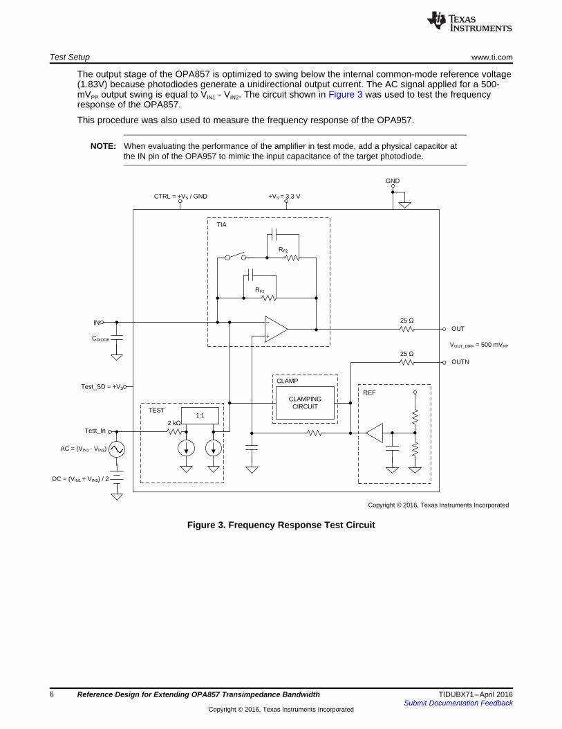
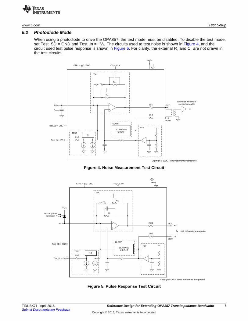
5.2 Photodiode ModeWhen using a photodiode to drive the OPA857, the test mode must be disabled. To disable the test mode,set Test_SD = GND and Test_In = +VS. The circuits used to test noise is shown in Figure 4, and thecircuit used test pulse response is shown in Figure 5. For clarity, the external RF and CF are not drawn inthe test circuits.
Figure 4. Noise Measurement Test Circuit
Figure 5. Pulse Response Test Circuit
Frequency (Hz)
Out
put (
dB)
-4
-3
-2
-1
0
1
2
3
4
1M 10M 100M 1G
D003
RF = 20 k: (Internal) || 6.8 k: (External)RF = 5 k: (Internal) || 6.8 k: (External)
Frequency (Hz)
Out
put (
dB)
-2
-1.5
-1
-0.5
0
0.5
1
1.5
2
1M 10M 100M
D004
RF(Internal) = 20 k:, RF || CF(External) = 6.8 k: || 0.1 pFRF(Internal) = 5 k:, RF || CF(External) = 6.8 k: || 0.1 pF
Frequency (Hz)
Out
put (
dB)
-4
-3
-2
-1
0
1
2
3
1M 10M 100M 1G
D001
Internal RF = 20 k:Internal RF = 5 k:
Frequency (Hz)O
utpu
t (dB
)
-4
-3
-2
-1
0
1
2
3
1M 10M 100M 1G
D002
RF = 20 k: (Internal) || 20 k: (External)RF = 5 k: (Internal) || 20 k: (External)
Test Data www.ti.com
8 TIDUBX71–April 2016Submit Documentation Feedback
Copyright © 2016, Texas Instruments Incorporated
Reference Design for Extending OPA857 Transimpedance Bandwidth
6 Test Data
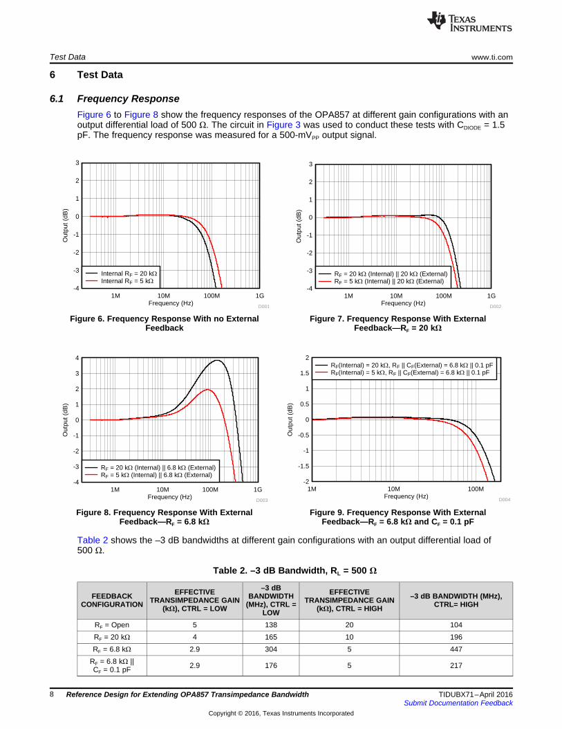
6.1 Frequency ResponseFigure 6 to Figure 8 show the frequency responses of the OPA857 at different gain configurations with anoutput differential load of 500 Ω. The circuit in Figure 3 was used to conduct these tests with CDIODE = 1.5pF. The frequency response was measured for a 500-mVPP output signal.
Figure 6. Frequency Response With no ExternalFeedback
Figure 7. Frequency Response With ExternalFeedback—RF = 20 kΩ
Figure 8. Frequency Response With ExternalFeedback—RF = 6.8 kΩ
Figure 9. Frequency Response With ExternalFeedback—RF = 6.8 kΩ and CF = 0.1 pF
Table 2 shows the –3 dB bandwidths at different gain configurations with an output differential load of500 Ω.
Table 2. –3 dB Bandwidth, RL = 500 Ω
FEEDBACKCONFIGURATION
EFFECTIVETRANSIMPEDANCE GAIN
(kΩ), CTRL = LOW
–3 dBBANDWIDTH
(MHz), CTRL =LOW
EFFECTIVETRANSIMPEDANCE GAIN
(kΩ), CTRL = HIGH–3 dB BANDWIDTH (MHz),
CTRL= HIGH
RF = Open 5 138 20 104RF = 20 kΩ 4 165 10 196RF = 6.8 kΩ 2.9 304 5 447
RF = 6.8 kΩ ||CF = 0.1 pF 2.9 176 5 217
Frequency (Hz)
Out
put (
dB)
-4
-3
-2
-1
0
1
2
3
4
1M 10M 100M 1G
D007
RF(Internal) = 20 k:, RF || CF(External) = 6.8 k: || 0.1 pFRF(Internal) = 5 k:, RF || CF(External) = 6.8 k: || 0.1 pF
Frequency (Hz)
Out
put (
dB)
-4
-3
-2
-1
0
1
2
3
1M 10M 100M 1G
D005
RF = 20 k: (Internal)RF = 5 k: (Internal)
Frequency (Hz)
Out
put (
dB)
-4
-3
-2
-1
0
1
2
3
1M 10M 100M 1G
D006
RF = 20 k: (Internal) || 20 k: (External)RF = 5 k: (Internal) || 20 k: (External)
www.ti.com Test Data
9TIDUBX71–April 2016Submit Documentation Feedback
Copyright © 2016, Texas Instruments Incorporated
Reference Design for Extending OPA857 Transimpedance Bandwidth
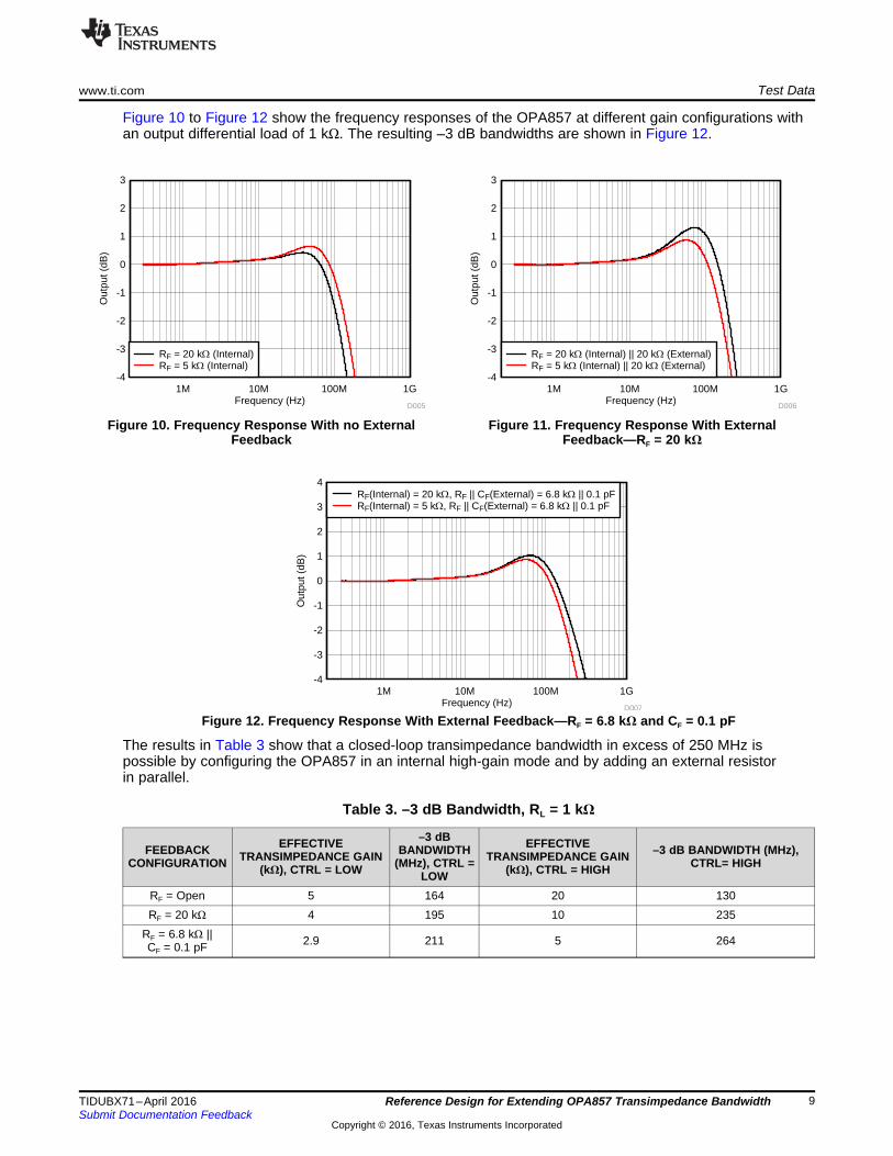
Figure 10 to Figure 12 show the frequency responses of the OPA857 at different gain configurations withan output differential load of 1 kΩ. The resulting –3 dB bandwidths are shown in Figure 12.
Figure 10. Frequency Response With no ExternalFeedback
Figure 11. Frequency Response With ExternalFeedback—RF = 20 kΩ
Figure 12. Frequency Response With External Feedback—RF = 6.8 kΩ and CF = 0.1 pF
The results in Table 3 show that a closed-loop transimpedance bandwidth in excess of 250 MHz ispossible by configuring the OPA857 in an internal high-gain mode and by adding an external resistorin parallel.
Table 3. –3 dB Bandwidth, RL = 1 kΩ
FEEDBACKCONFIGURATION
EFFECTIVETRANSIMPEDANCE GAIN
(kΩ), CTRL = LOW
–3 dBBANDWIDTH
(MHz), CTRL =LOW
EFFECTIVETRANSIMPEDANCE GAIN
(kΩ), CTRL = HIGH–3 dB BANDWIDTH (MHz),
CTRL= HIGH
RF = Open 5 164 20 130RF = 20 kΩ 4 195 10 235
RF = 6.8 kΩ ||CF = 0.1 pF 2.9 211 5 264
Frequency (Hz)
Inpu
t Ref
erre
d N
oise
(nV
/�H
z)
0
0.5
1
1.5
2
2.5
3
3.5
4
1M 10M 100M
D009
Internal RF= 5 k:Internal RF= 20 k:
Frequency (Hz)
Inpu
t Ref
erre
d N
oise
(nV
/�H
z)
0
0.5
1
1.5
2
2.5
3
3.5
4
1M 10M 100M
D010
RF(Internal) = 5 k:, RF || CF(External) = 6.8 k: || 0.1 pFRF(Internal) = 20 k:, RF || CF(External) = 6.8 k: || 0.1 pF
Time (50ns/div)
Out
put V
olta
ge (
V)
D008
RF = 5 k: (Internal), RF || CF (External) = 6.8 k: || 0.1 pFRF = 20 k: (Internal), RF || CF (External)= 6.8 k: || 0.1 pF
Test Data www.ti.com
10 TIDUBX71–April 2016Submit Documentation Feedback
Copyright © 2016, Texas Instruments Incorporated
Reference Design for Extending OPA857 Transimpedance Bandwidth
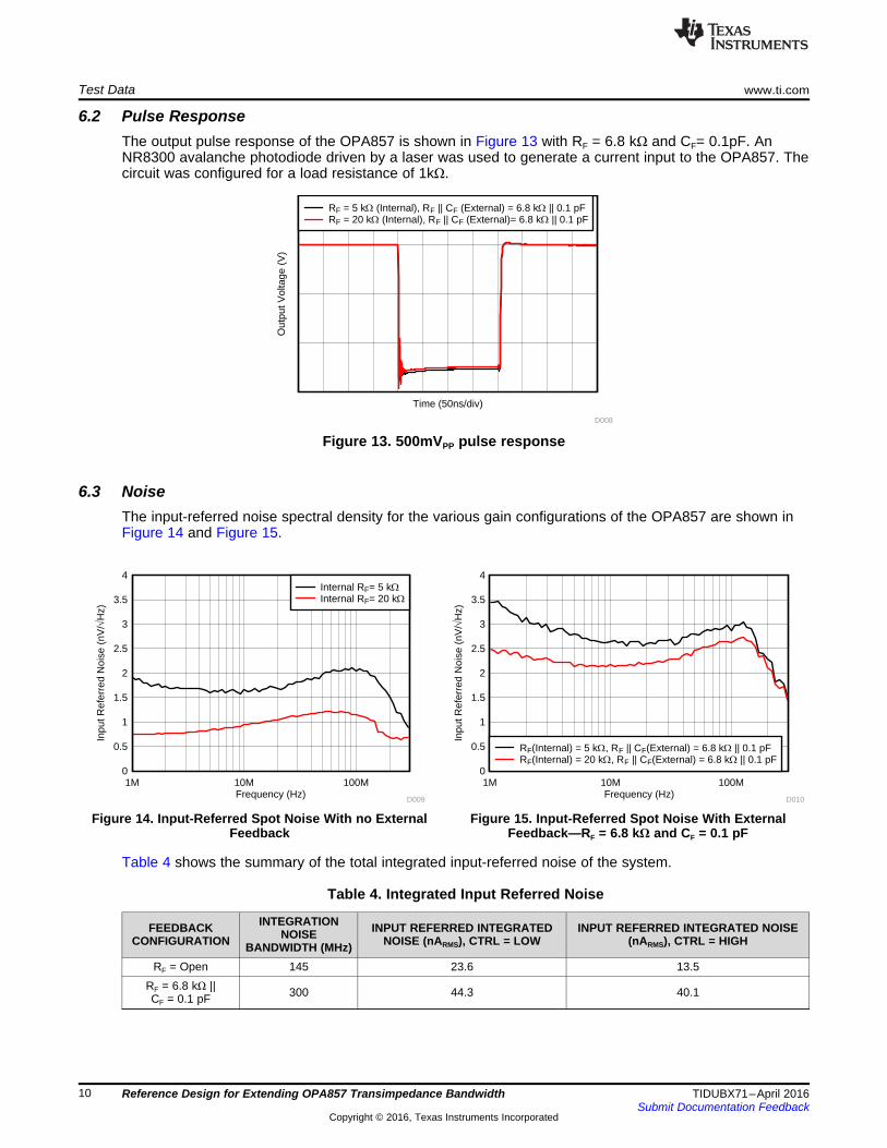
6.2 Pulse ResponseThe output pulse response of the OPA857 is shown in Figure 13 with RF = 6.8 kΩ and CF= 0.1pF. AnNR8300 avalanche photodiode driven by a laser was used to generate a current input to the OPA857. Thecircuit was configured for a load resistance of 1kΩ.
Figure 13. 500mVPP pulse response
6.3 NoiseThe input-referred noise spectral density for the various gain configurations of the OPA857 are shown inFigure 14 and Figure 15.
Figure 14. Input-Referred Spot Noise With no ExternalFeedback
Figure 15. Input-Referred Spot Noise With ExternalFeedback—RF = 6.8 kΩ and CF = 0.1 pF
Table 4 shows the summary of the total integrated input-referred noise of the system.
Table 4. Integrated Input Referred Noise
FEEDBACKCONFIGURATION
INTEGRATIONNOISE
BANDWIDTH (MHz)INPUT REFERRED INTEGRATED
NOISE (nARMS), CTRL = LOWINPUT REFERRED INTEGRATED NOISE
(nARMS), CTRL = HIGH
RF = Open 145 23.6 13.5RF = 6.8 kΩ ||CF = 0.1 pF 300 44.3 40.1
P2
6095
P1
6095
+VCC TP1
TP2
2.2µFC1
GND
0.22 µFC2
0.01 µFC3
1000 ohm
L1
Test_In1
2 3 4 5
J1
P3
6095
0.1µF
100V
C4
GND
0.01 µF
100V
C5
0
R1
VAPD
TP3
1
2
3
J5
61300311121
+VCC
GND
1
2
3
J6
61300311121
+VCC
GND
1
2345
J2
SH-J4
SH-J5
VOUTN
1
2345
J3
VOUTP
20k
5k
Test
APD49.9R3
56.2R8
3.9pFC7
0R2
GND
1.5pFC6
0R9
0R10
1
2
J7 0
R11
0
R12
0R14
GAINMODE
GND
1
2
J4SH-J6
DNI
DNI
DNI
CTRL2
GND1
GND3
GND4
GND6
GND7
GND12
IN15
NC16
OUT8
OUTN5
PAD17
TEST_IN/VS+14
TEST_SD/GND13
VS+9
VS+10
VS+11 U1
OPA857IRGTRGND
+VCC
TEST_IN
TEST_SD CTRL
TEST_SD
CTRL
VAPD
0
R13
GND
TEST_IN
+VCC
21 3
D1
0R15
1
2
3 4
NC5
6
T1 ADT1-1WT+
0.1pFC8
0.1pFC9
DNI
DNI
3.40k
R4
3.40k
R5
487
R6
487
R7
Copyright © 2016, Texas Instruments Incorporated
www.ti.com Design Files
11TIDUBX71–April 2016Submit Documentation Feedback
Copyright © 2016, Texas Instruments Incorporated
Reference Design for Extending OPA857 Transimpedance Bandwidth
7 Design Files
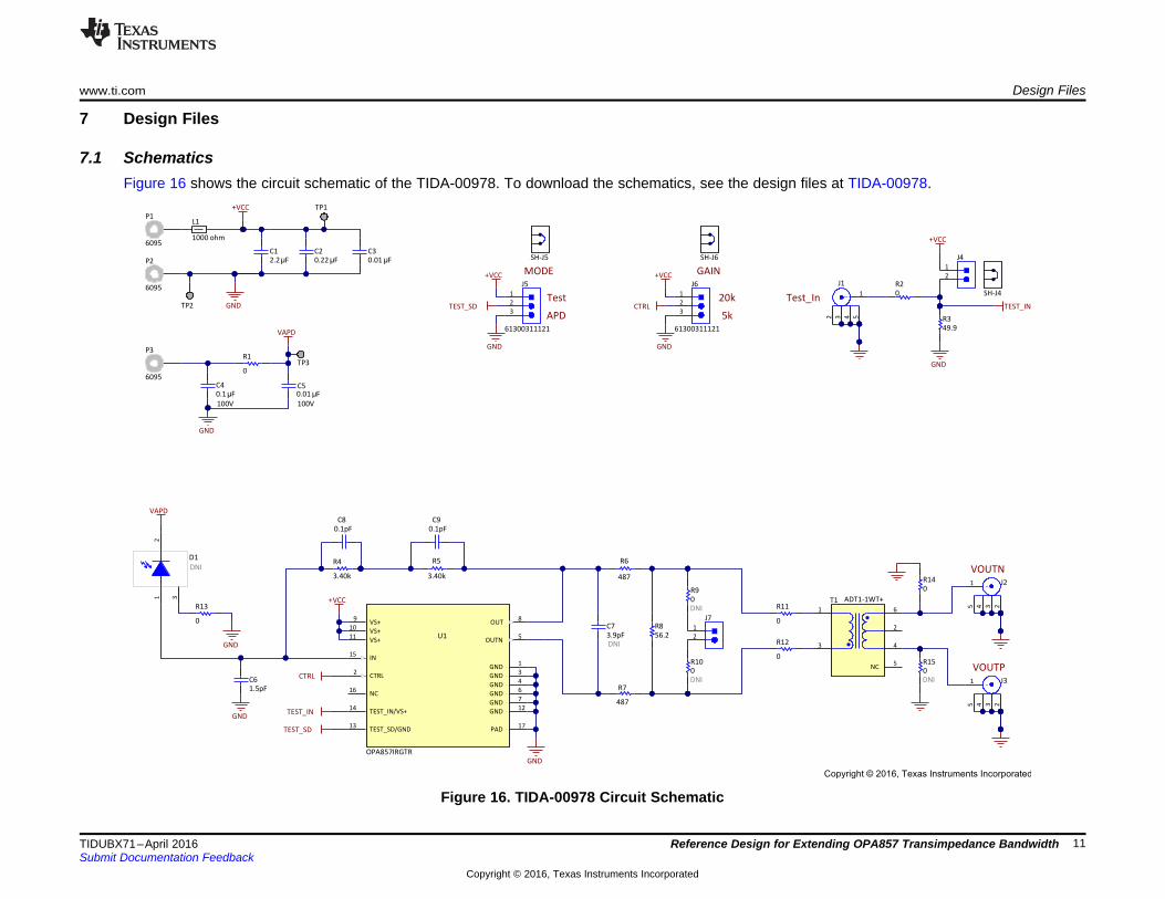
7.1 SchematicsFigure 16 shows the circuit schematic of the TIDA-00978. To download the schematics, see the design files at TIDA-00978.
Figure 16. TIDA-00978 Circuit Schematic
Copyright © 2016, Texas Instruments Incorporated
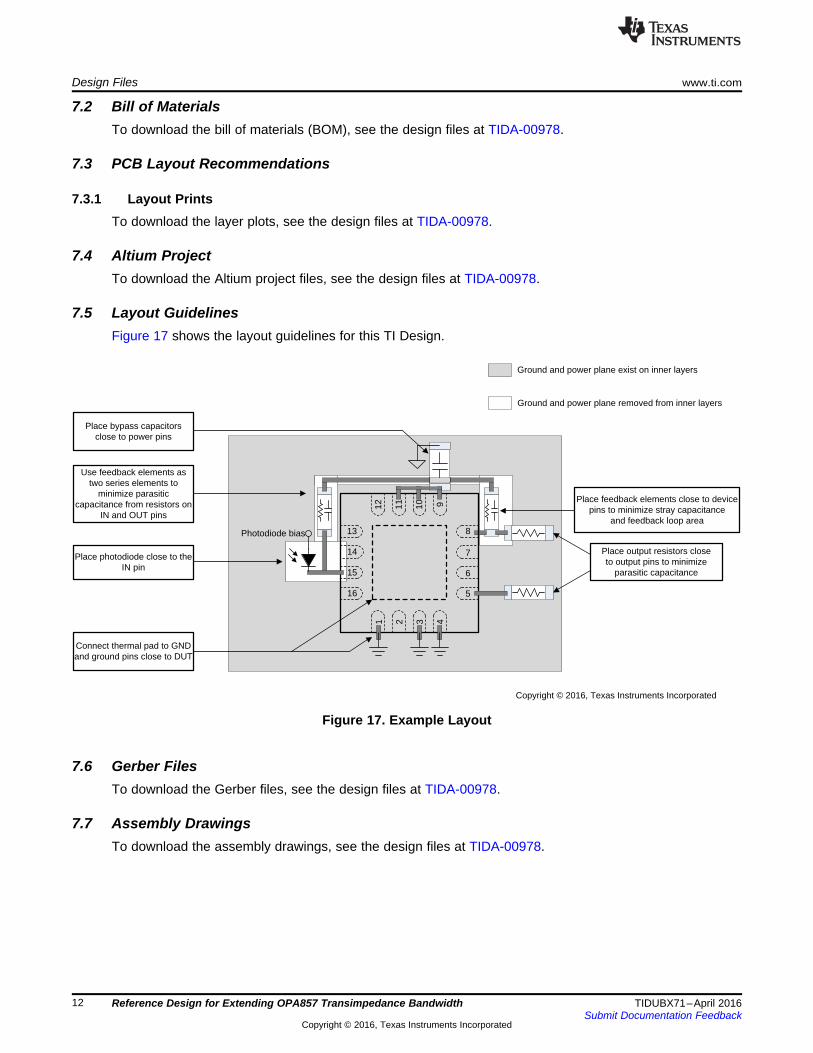
Use feedback elements as two series elements to
minimize parasitic capacitance from resistors on
IN and OUT pins
Place bypass capacitors close to power pins
Place feedback elements close to device pins to minimize stray capacitance
and feedback loop area
Place output resistors close to output pins to minimize
parasitic capacitance
13 8
7
6
5
12 11 10 9
1 2 3 4
Connect thermal pad to GND and ground pins close to DUT
14
15
16
Photodiode bias
Place photodiode close to the IN pin
Ground and power plane exist on inner layers
Ground and power plane removed from inner layers
Design Files www.ti.com
12 TIDUBX71–April 2016Submit Documentation Feedback
Copyright © 2016, Texas Instruments Incorporated
Reference Design for Extending OPA857 Transimpedance Bandwidth
7.2 Bill of MaterialsTo download the bill of materials (BOM), see the design files at TIDA-00978.
7.3 PCB Layout Recommendations
7.3.1 Layout PrintsTo download the layer plots, see the design files at TIDA-00978.
7.4 Altium ProjectTo download the Altium project files, see the design files at TIDA-00978.
7.5 Layout GuidelinesFigure 17 shows the layout guidelines for this TI Design.
Figure 17. Example Layout
7.6 Gerber FilesTo download the Gerber files, see the design files at TIDA-00978.
7.7 Assembly DrawingsTo download the assembly drawings, see the design files at TIDA-00978.
www.ti.com References
13TIDUBX71–April 2016Submit Documentation Feedback
Copyright © 2016, Texas Instruments Incorporated
Reference Design for Extending OPA857 Transimpedance Bandwidth
8 References
1. Texas Instruments, What you need to know about transimpedance amplifiers – part 1, Article (TIE2E™ Community)
9 About the AuthorSAMIR CHERIAN is an applications engineer with TI in the High-Speed Amplifier division in Tucson,Arizona. He validates the performance and specifications of high-speed amplifiers and provides customersupport through TI online forums, application notes, and reference designs.

IMPORTANT NOTICE FOR TI REFERENCE DESIGNS
Texas Instruments Incorporated (‘TI”) reference designs are solely intended to assist designers (“Designer(s)”) who are developing systemsthat incorporate TI products. TI has not conducted any testing other than that specifically described in the published documentation for aparticular reference design.TI’s provision of reference designs and any other technical, applications or design advice, quality characterization, reliability data or otherinformation or services does not expand or otherwise alter TI’s applicable published warranties or warranty disclaimers for TI products, andno additional obligations or liabilities arise from TI providing such reference designs or other items.TI reserves the right to make corrections, enhancements, improvements and other changes to its reference designs and other items.Designer understands and agrees that Designer remains responsible for using its independent analysis, evaluation and judgment indesigning Designer’s systems and products, and has full and exclusive responsibility to assure the safety of its products and compliance ofits products (and of all TI products used in or for such Designer’s products) with all applicable regulations, laws and other applicablerequirements. Designer represents that, with respect to its applications, it has all the necessary expertise to create and implementsafeguards that (1) anticipate dangerous consequences of failures, (2) monitor failures and their consequences, and (3) lessen thelikelihood of failures that might cause harm and take appropriate actions. Designer agrees that prior to using or distributing any systemsthat include TI products, Designer will thoroughly test such systems and the functionality of such TI products as used in such systems.Designer may not use any TI products in life-critical medical equipment unless authorized officers of the parties have executed a specialcontract specifically governing such use. Life-critical medical equipment is medical equipment where failure of such equipment would causeserious bodily injury or death (e.g., life support, pacemakers, defibrillators, heart pumps, neurostimulators, and implantables). Suchequipment includes, without limitation, all medical devices identified by the U.S. Food and Drug Administration as Class III devices andequivalent classifications outside the U.S.Designers are authorized to use, copy and modify any individual TI reference design only in connection with the development of endproducts that include the TI product(s) identified in that reference design. HOWEVER, NO OTHER LICENSE, EXPRESS OR IMPLIED, BYESTOPPEL OR OTHERWISE TO ANY OTHER TI INTELLECTUAL PROPERTY RIGHT, AND NO LICENSE TO ANY TECHNOLOGY ORINTELLECTUAL PROPERTY RIGHT OF TI OR ANY THIRD PARTY IS GRANTED HEREIN, including but not limited to any patent right,copyright, mask work right, or other intellectual property right relating to any combination, machine, or process in which TI products orservices are used. Information published by TI regarding third-party products or services does not constitute a license to use such productsor services, or a warranty or endorsement thereof. Use of the reference design or other items described above may require a license from athird party under the patents or other intellectual property of the third party, or a license from TI under the patents or other intellectualproperty of TI.TI REFERENCE DESIGNS AND OTHER ITEMS DESCRIBED ABOVE ARE PROVIDED “AS IS” AND WITH ALL FAULTS. TI DISCLAIMSALL OTHER WARRANTIES OR REPRESENTATIONS, EXPRESS OR IMPLIED, REGARDING THE REFERENCE DESIGNS OR USE OFTHE REFERENCE DESIGNS, INCLUDING BUT NOT LIMITED TO ACCURACY OR COMPLETENESS, TITLE, ANY EPIDEMIC FAILUREWARRANTY AND ANY IMPLIED WARRANTIES OF MERCHANTABILITY, FITNESS FOR A PARTICULAR PURPOSE, AND NON-INFRINGEMENT OF ANY THIRD PARTY INTELLECTUAL PROPERTY RIGHTS.TI SHALL NOT BE LIABLE FOR AND SHALL NOT DEFEND OR INDEMNIFY DESIGNERS AGAINST ANY CLAIM, INCLUDING BUT NOTLIMITED TO ANY INFRINGEMENT CLAIM THAT RELATES TO OR IS BASED ON ANY COMBINATION OF PRODUCTS ASDESCRIBED IN A TI REFERENCE DESIGN OR OTHERWISE. IN NO EVENT SHALL TI BE LIABLE FOR ANY ACTUAL, DIRECT,SPECIAL, COLLATERAL, INDIRECT, PUNITIVE, INCIDENTAL, CONSEQUENTIAL OR EXEMPLARY DAMAGES IN CONNECTION WITHOR ARISING OUT OF THE REFERENCE DESIGNS OR USE OF THE REFERENCE DESIGNS, AND REGARDLESS OF WHETHER TIHAS BEEN ADVISED OF THE POSSIBILITY OF SUCH DAMAGES.TI’s standard terms of sale for semiconductor products (http://www.ti.com/sc/docs/stdterms.htm) apply to the sale of packaged integratedcircuit products. Additional terms may apply to the use or sale of other types of TI products and services.Designer will fully indemnify TI and its representatives against any damages, costs, losses, and/or liabilities arising out of Designer’s non-compliance with the terms and provisions of this Notice.IMPORTANT NOTICE
Mailing Address: Texas Instruments, Post Office Box 655303, Dallas, Texas 75265Copyright © 2016, Texas Instruments Incorporated