Reducing DRAM Latency at Low Cost by Exploiting...
81
Reducing DRAM Latency at Low Cost by Exploiting Heterogeneity Donghyuk Lee Carnegie Mellon University
Transcript of Reducing DRAM Latency at Low Cost by Exploiting...

Reducing DRAM Latency at Low Cost by Exploiting Heterogeneity
Donghyuk Lee
Carnegie Mellon University
2
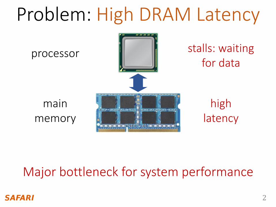
Problem: High DRAM Latency
processor
main memory
high latency
Major bottleneck for system performance
stalls: waitingfor data
3
0
20
40
60
80
100
0.0
0.5
1.0
1.5
2.0
2.5
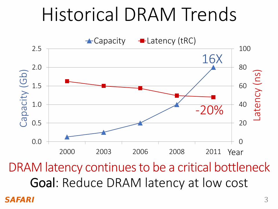
2000 2003 2006 2008 2011
Late
ncy
(n
s)
Cap
acit
y (G
b)
Year
Capacity Latency (tRC)
16X
-20%
Historical DRAM Trends
DRAM latency continues to be a critical bottleneckGoal: Reduce DRAM latency at low cost
4
Why is DRAM slow?
5
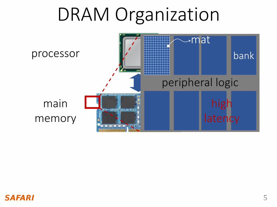
processor
main memory
peripheral logic
bank
mat
high latency
DRAM Organization

6
DRAM Cell Array: Mat
peripheral logic
cell
matmat
sense amplifierw
ord
line
driver
cell
wordline
bitline
7
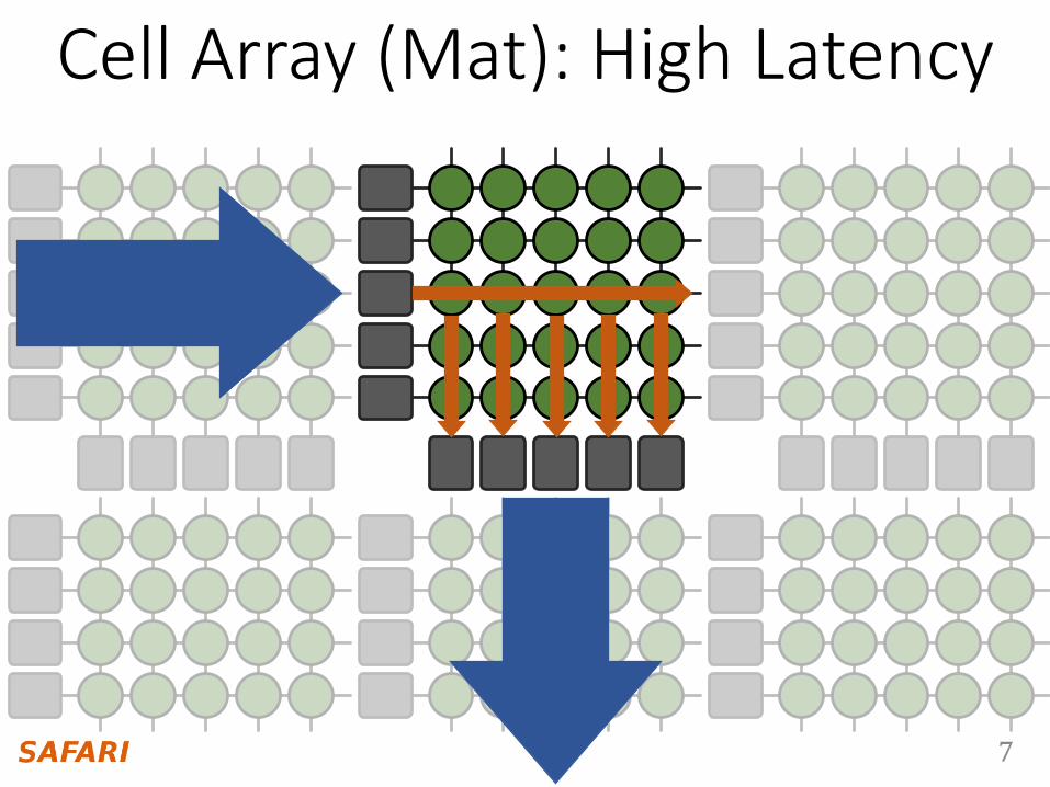
Cell Array (Mat): High Latency

8
DRAM Cell Array: High Latency
Outside mat
Inside mat
• Narrow poly wire– Large resistance– Large capacitance Slow
• Small cell – Difficult to detect
data in small cell Slow
• Thick metal wire– Small resistance– Small capacitance Fast

9
DRAM cell array (mat) is the dominant latency bottleneck
due to three reasons
10
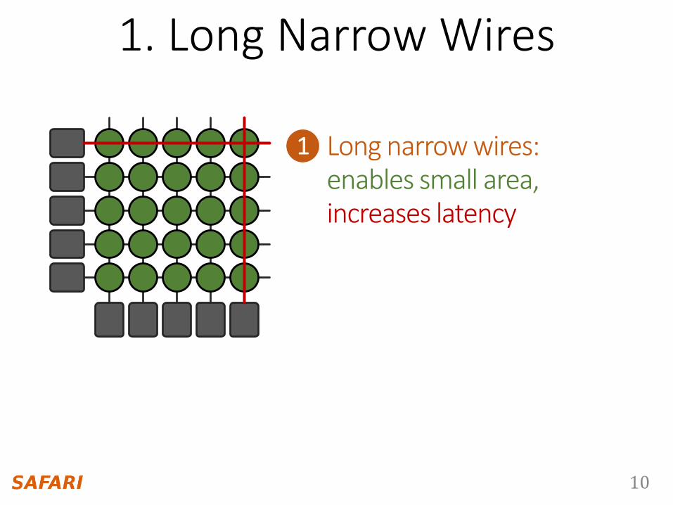
1. Long Narrow Wires
1 Long narrow wires:enables small area,increases latency
11
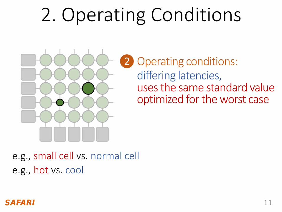
2. Operating Conditions
2 Operating conditions:differing latencies,uses the same standard value optimized for the worst case
e.g., small cell vs. normal cell
e.g., hot vs. cool

12
3. Distance from Peripheral Logic
3 Distance from peripheral logic:differing latenciesuses the same standard value optimized for the farthest cell
e.g., near cell vs. far cell

13
Three Sources of High Latency
2 Operating conditions
3 Distance from peripheral logic
1 Long narrow wires
Goal: Reduce DRAM latency at low cost with three approaches
AL-DRAM
AVA-DRAM
TL-DRAM
14
Thesis Statement
DRAM latency can be reduced by enabling and exploiting
latency heterogeneity in DRAM

15
Tiered-Latency DRAM:Lowering Latency by Modifying the Bitline Architecture
Approach 1
Lee et al., Tiered-Latency DRAM: A Low Latency and Low Cost DRAM Architecture, HPCA 2013
Outline
Prior Work
Future Research Direction
1. TL-DRAM Reducing DRAM Latency by Modifying Bitline Architecture
2. AL-DRAM Optimizing DRAM Latency for the Common-Case
3. AVA-DRAM Lowering DRAM Latencyby Exploiting Architectural Variation
Reducing DRAM Latency by Modifying Bitline Architecture1. TL-DRAM
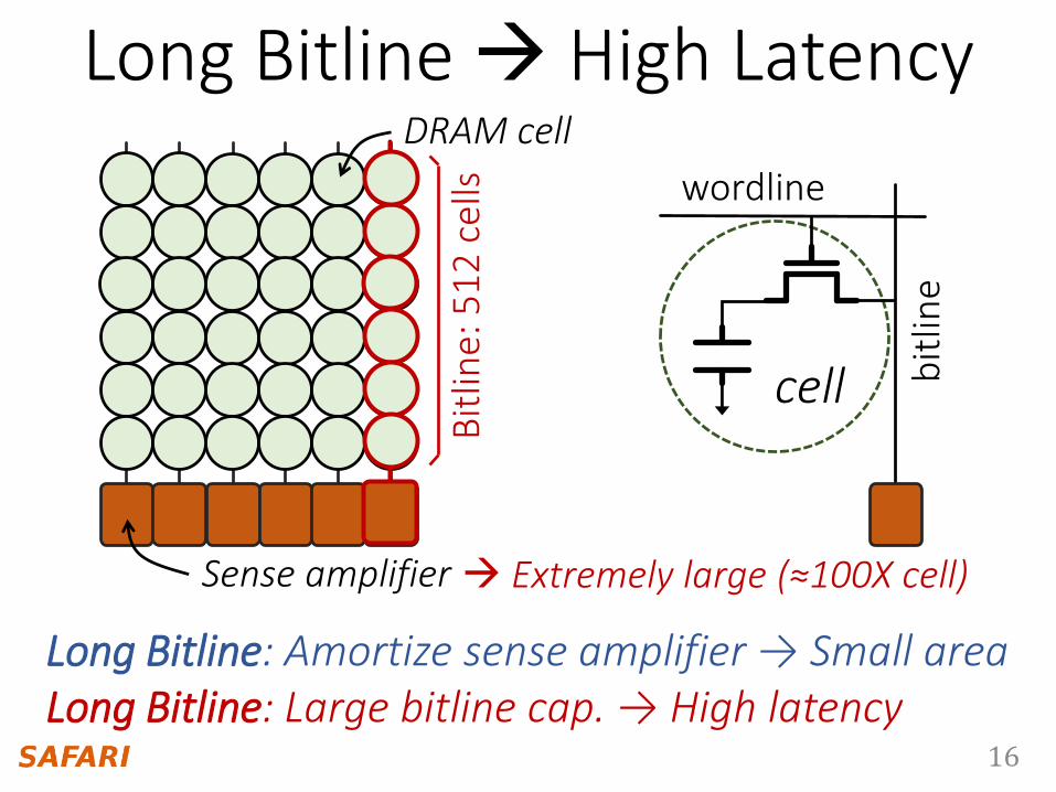
16
Extremely large (≈100X cell)
Long Bitline: Amortize sense amplifier → Small areaLong Bitline: Large bitline cap. → High latency
Long Bitline High LatencyDRAM cell
Sense amplifier
wordline
bit
line
cell
Bit
line:
51
2 c
ells
17
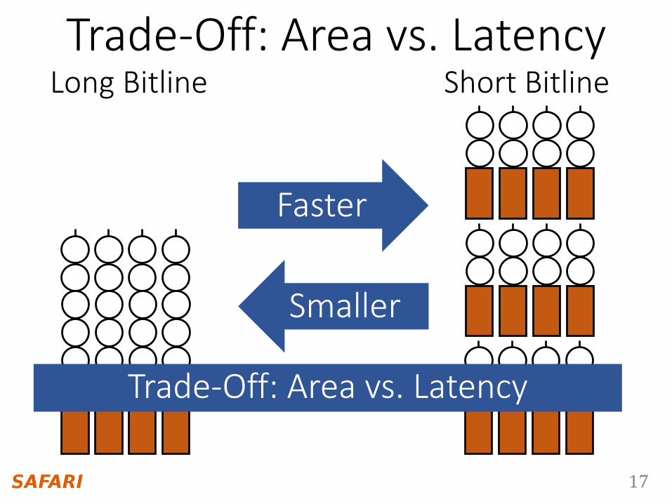
Faster
Smaller
Short BitlineLong Bitline
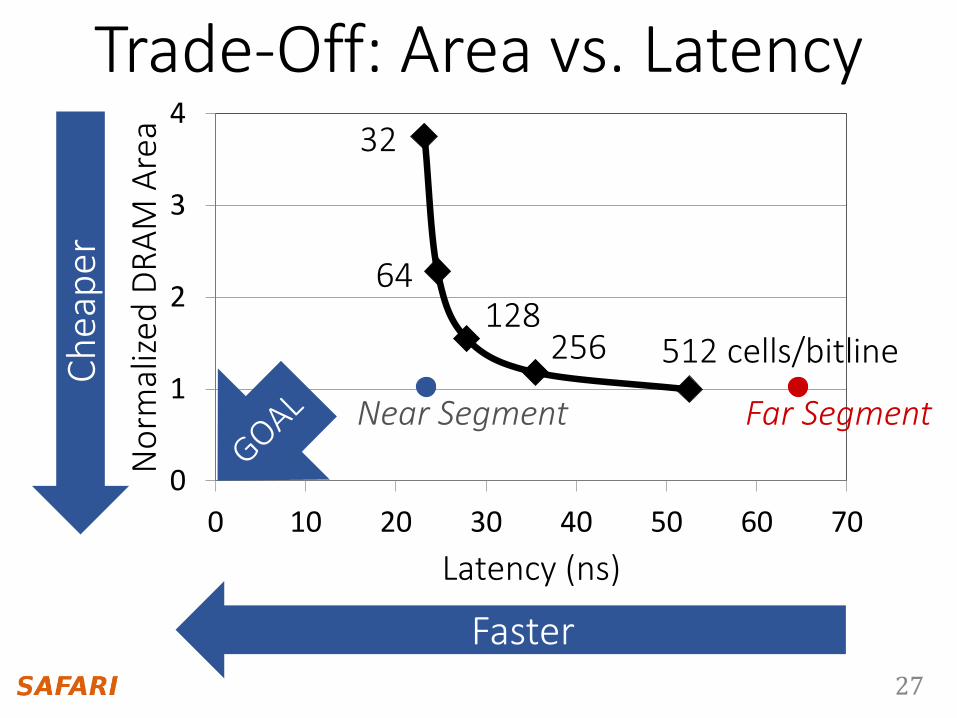
Trade-Off: Area vs. Latency
Trade-Off: Area vs. Latency

18
0
1
2
3
4
0 10 20 30 40 50 60 70
No
rmal
ized
DR
AM
Are
a
Latency (ns)
64
32
128
256 512 cells/bitline
Commodity DRAM
Long Bitline
Ch
eap
er
Faster
Fancy DRAMShort Bitline
Trade-Off: Area vs. Latency
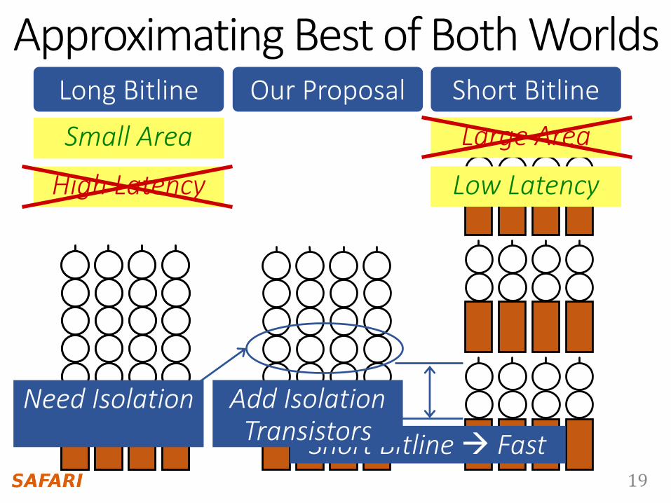
19
Short Bitline
Low Latency
Long Bitline
Small Area
Long Bitline
Low Latency
Short BitlineOur Proposal
Small Area
Short Bitline Fast
Need Isolation Add Isolation Transistors
High Latency
Large Area
Approximating Best of Both Worlds
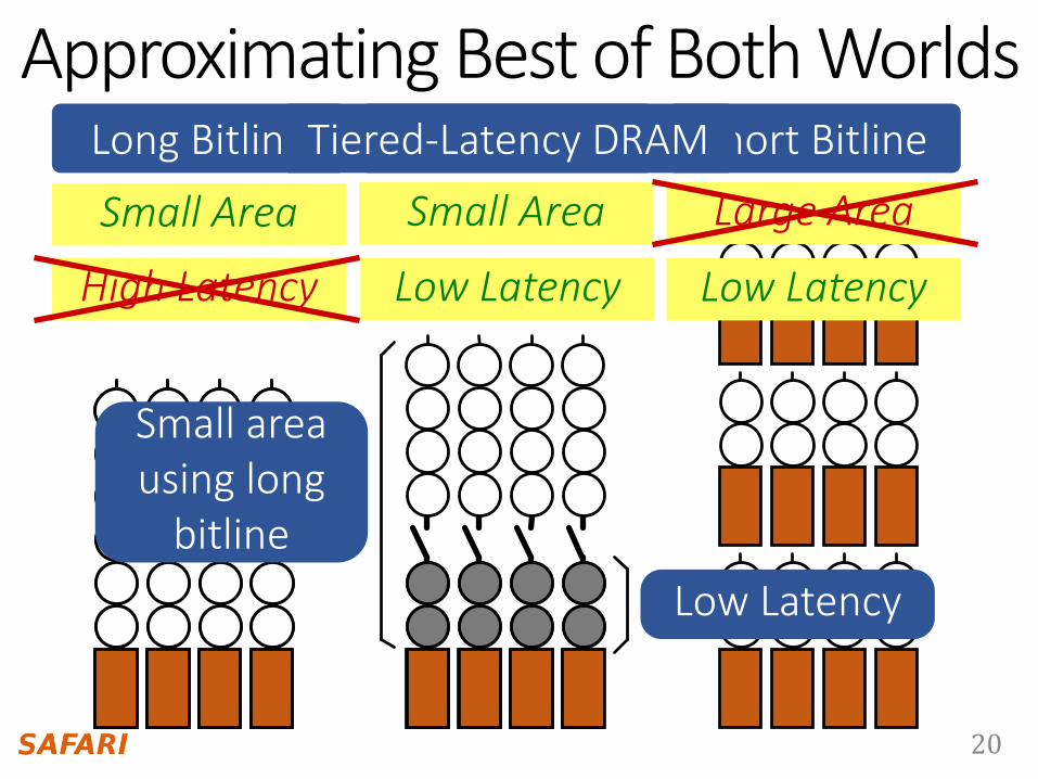
20
Low Latency
Our Proposal
Small Area
Long Bitline
Small Area
Long Bitline
High Latency
Short Bitline
Low Latency
Short Bitline
Large Area
Tiered-Latency DRAM
Low Latency
Small area using long
bitline
Approximating Best of Both Worlds
21
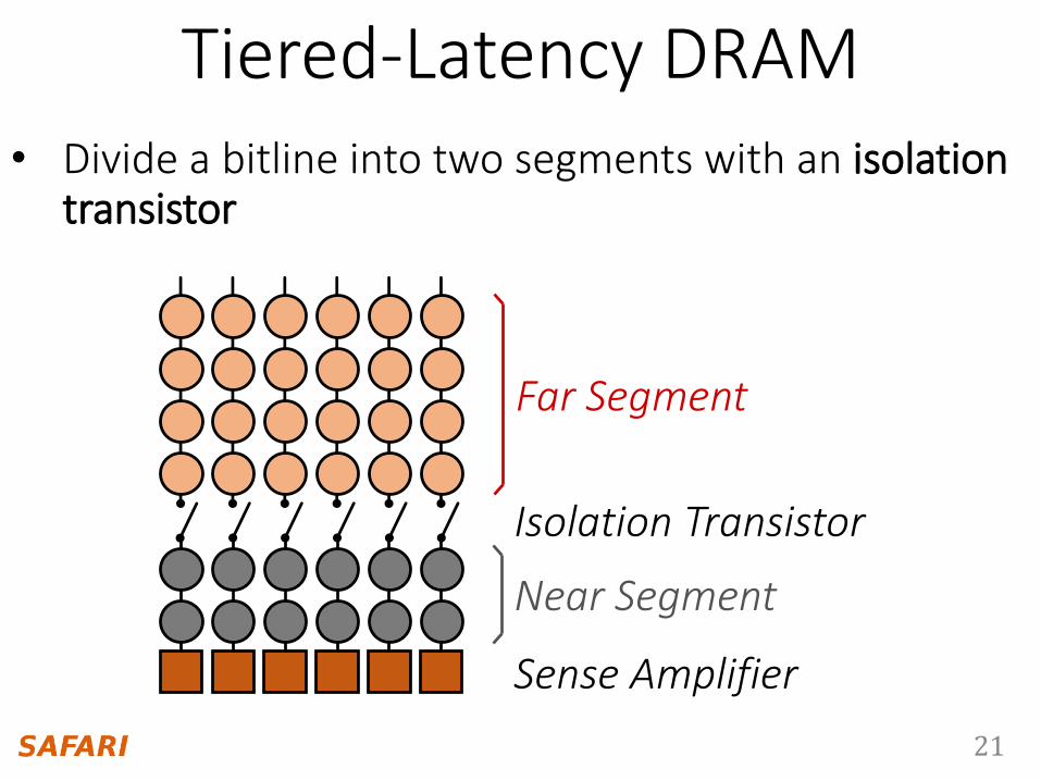
Near Segment
Far Segment
Isolation Transistor
• Divide a bitline into two segments with an isolation transistor
Sense Amplifier
Tiered-Latency DRAM

22
Far SegmentFar Segment
Near Segment
Isolation Transistor
• Turn off the isolation transistor
Isolation Transistor (off)
Sense Amplifier
Near Segment Access
Reduced bitline capacitance
Low latency & low power
Reduced bitline length
23
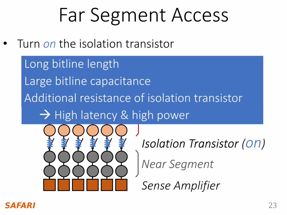
Near SegmentNear Segment
• Turn on the isolation transistor
Far Segment
Isolation TransistorIsolation Transistor (on)
Sense Amplifier
Far Segment Access
Large bitline capacitance
Additional resistance of isolation transistor
Long bitline length
High latency & high power
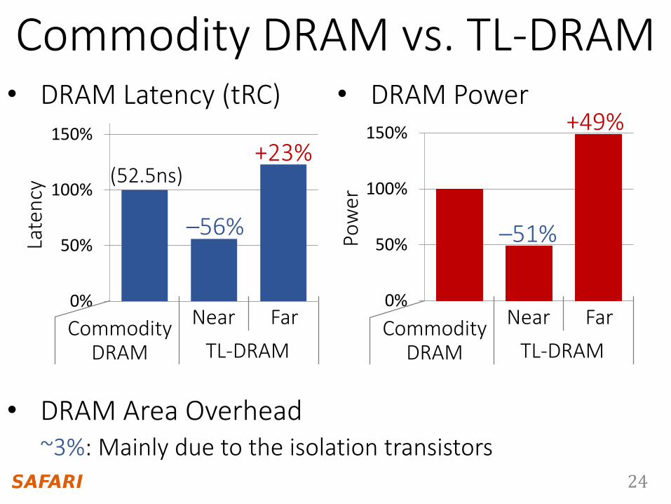
24
0%
50%
100%
150%
0%
50%
100%
150%
Late
ncy
Pow
er
–56%
+23%
–51%
+49%• DRAM Latency (tRC) • DRAM Power
• DRAM Area Overhead~3%: Mainly due to the isolation transistors
TL-DRAMCommodity
DRAM
Near Far Commodity DRAM
Near Far
TL-DRAM
(52.5ns)
Commodity DRAM vs. TL-DRAM
25
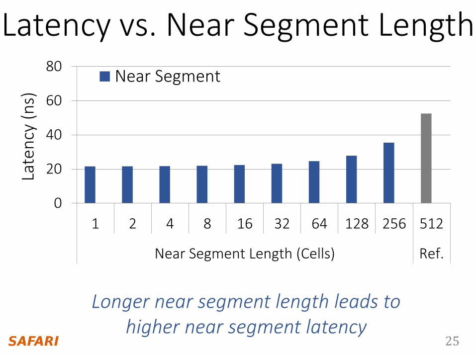
0
20
40
60
80
1 2 4 8 16 32 64 128 256 512
Near Segment Length (Cells) Ref.
Near Segment Far Segment
Late
ncy
(n
s)
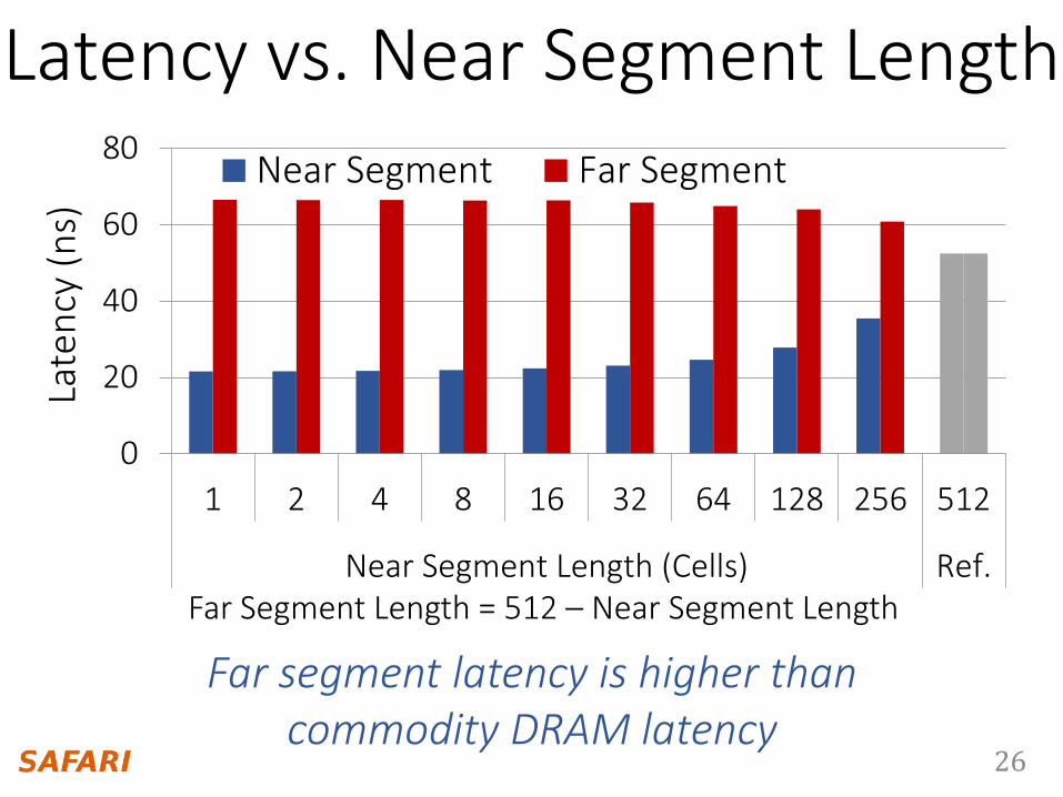
Longer near segment length leads to higher near segment latency
Latency vs. Near Segment Length
26
0
20
40
60
80
1 2 4 8 16 32 64 128 256 512
Near Segment Length (Cells) Ref.
Near Segment Far Segment
Late
ncy
(n
s)
Far segment latency is higher than commodity DRAM latency
Far Segment Length = 512 – Near Segment Length
Latency vs. Near Segment Length
27
0
1
2
3
4
0 10 20 30 40 50 60 70
No
rmal
ized
DR
AM
Are
a
Latency (ns)
64
32
128256 512 cells/bitlineC
hea
per
Faster
Near Segment Far Segment
Trade-Off: Area vs. Latency
28
• TL-DRAM is a substrate that can be leveraged by the hardware and/or software
– Use near segment as hardware-managed cache to far segment
Leveraging Tiered-Latency DRAM
29
0%
3%
6%
9%
12%
15%
0%
20%
40%
60%
80%
100%
IPC
Imp
rove
men
t
No
rmal
ized
En
ergy
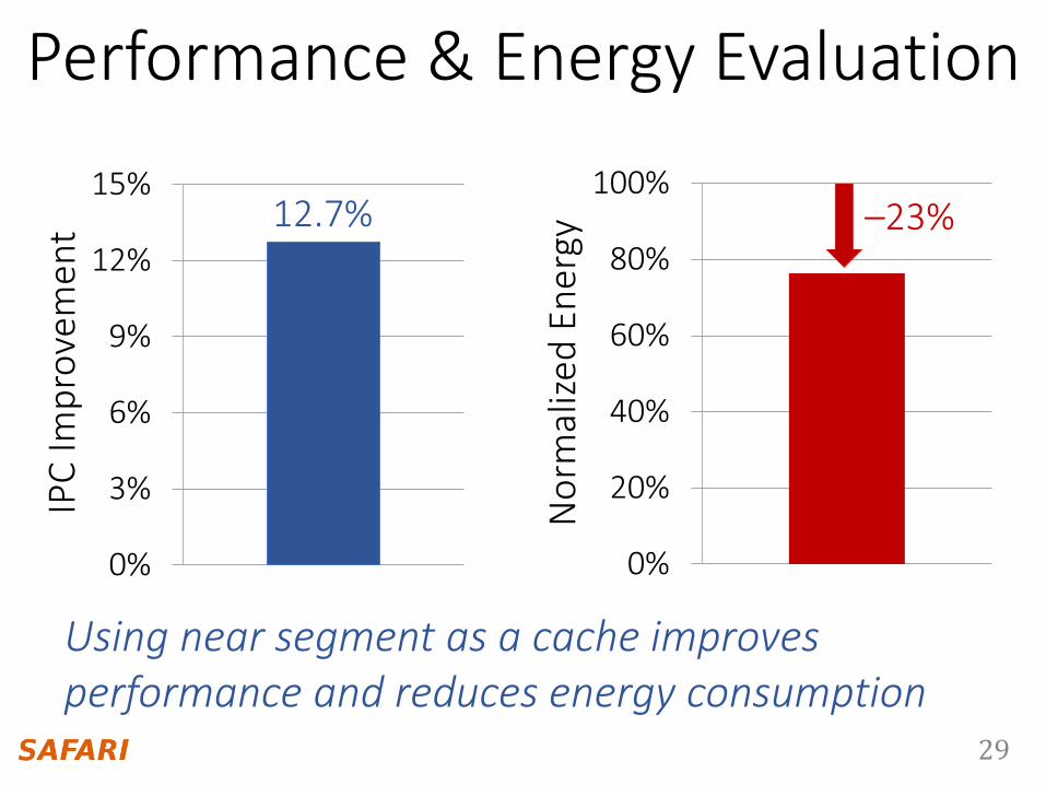
12.7% –23%
Using near segment as a cache improves performance and reduces energy consumption
Performance & Energy Evaluation
30
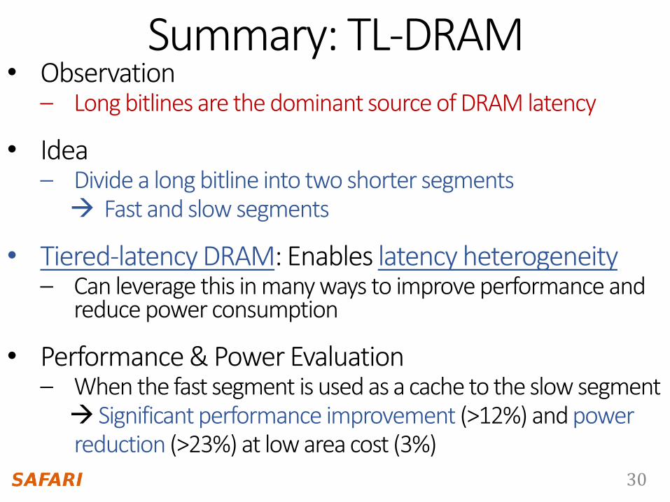
• Observation– Long bitlines are the dominant source of DRAM latency
• Idea– Divide a long bitline into two shorter segments Fast and slow segments
• Tiered-latency DRAM: Enables latency heterogeneity – Can leverage this in many ways to improve performance and
reduce power consumption
• Performance & Power Evaluation – When the fast segment is used as a cache to the slow segment Significant performance improvement (>12%) and power reduction (>23%) at low area cost (3%)
Summary: TL-DRAM

31
Adaptive-Latency DRAM:Optimizing DRAM Latencyfor the Common Operating Conditions
Approach 2
Lee et al., Adaptive-Latency DRAM: Optimizing DRAM Timing for the Common-Case, HPCA 2015
Outline
Prior Work
Future Research Direction
1. TL-DRAM Reducing DRAM Latency by Modifying Bitline Architecture
2. AL-DRAM Optimizing DRAM Latency for the Common-Case
3. AVA-DRAM Lowering DRAM Latencyby Exploiting Architectural Variation
Reducing DRAM Latency by Modifying Bitline Architecture1. TL-DRAM
Optimizing DRAM Latency for the Common Case2. AL-DRAM
32
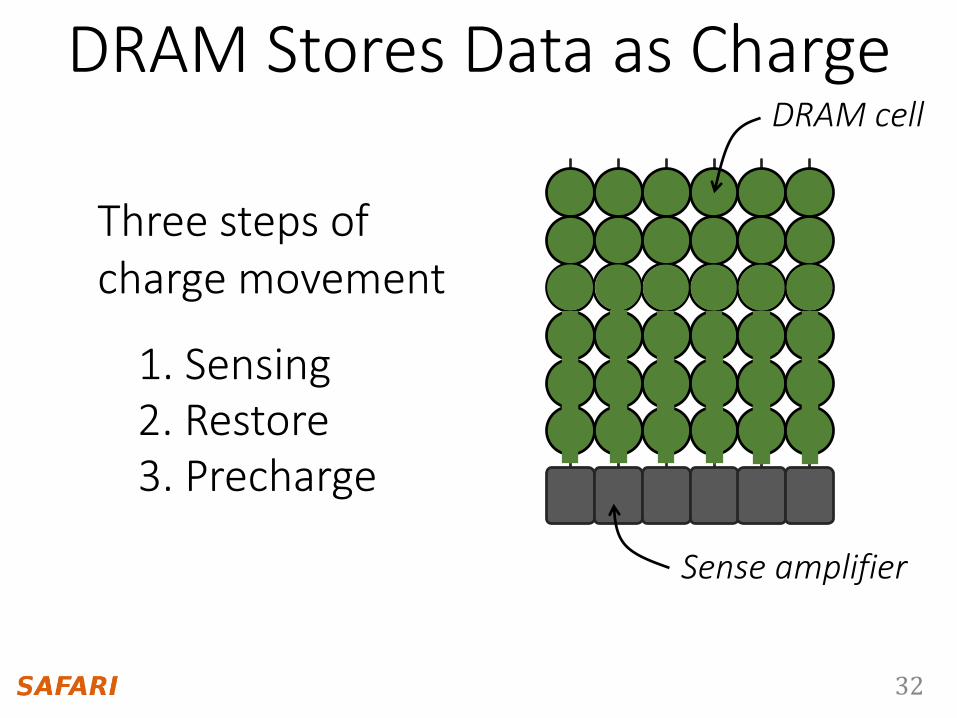
DRAM Stores Data as Charge
1. Sensing2. Restore3. Precharge
DRAM cell
Sense amplifier
Three steps of charge movement

33
Sensing RestoreTiming Parameters
Data 0
Data 1
cell
time
char
ge
Sense amplifier
DRAM Charge over Time
Why does DRAM need the extra timing margin?
In theory margin
cell
Sense amplifier
In practice
34
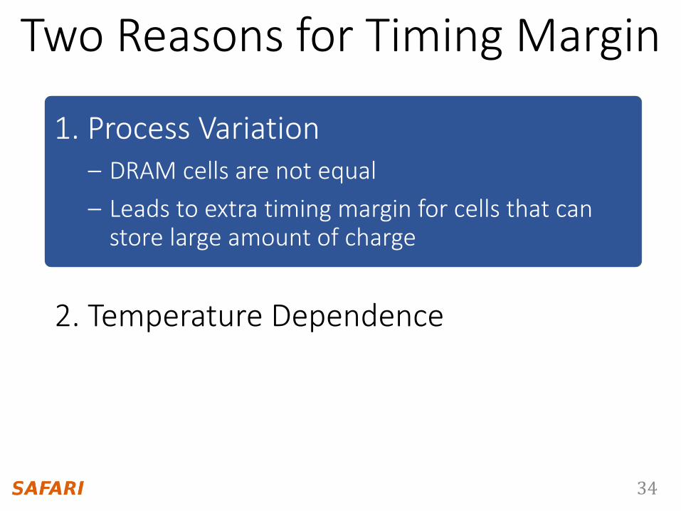
1. Process Variation – DRAM cells are not equal
– Leads to extra timing margin for cell that can store small amount of charge
2. Temperature Dependence – DRAM leaks more charge at higher temperature
– Leads to extra timing margin when operating at low temperature
Two Reasons for Timing Margin
1. Process Variation – DRAM cells are not equal
– Leads to extra timing margin for cell that can store small amount of charge;
1. Process Variation – DRAM cells are not equal
– Leads to extra timing margin for cells that can store large amount of charge

35
Same size Same charge
Different size Different charge
Same latency Different latency
Large variation in cell size Large variation in charge Large variation in access latency
DRAM Cells are Not EqualRealIdeal
Largest cell
Smallest cell
36
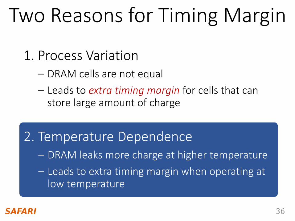
1. Process Variation – DRAM cells are not equal
– Leads to extra timing margin for cells that can store large amount of charge
2. Temperature Dependence – DRAM leaks more charge at higher temperature
– Leads to extra timing margin when operating at low temperature
Two Reasons for Timing Margin
2. Temperature Dependence – DRAM leaks more charge at higher temperature
– Leads to extra timing margin when operating at low temperature
2. Temperature Dependence – DRAM leaks more charge at higher temperature
– Leads to extra timing margin when operating at low temperature
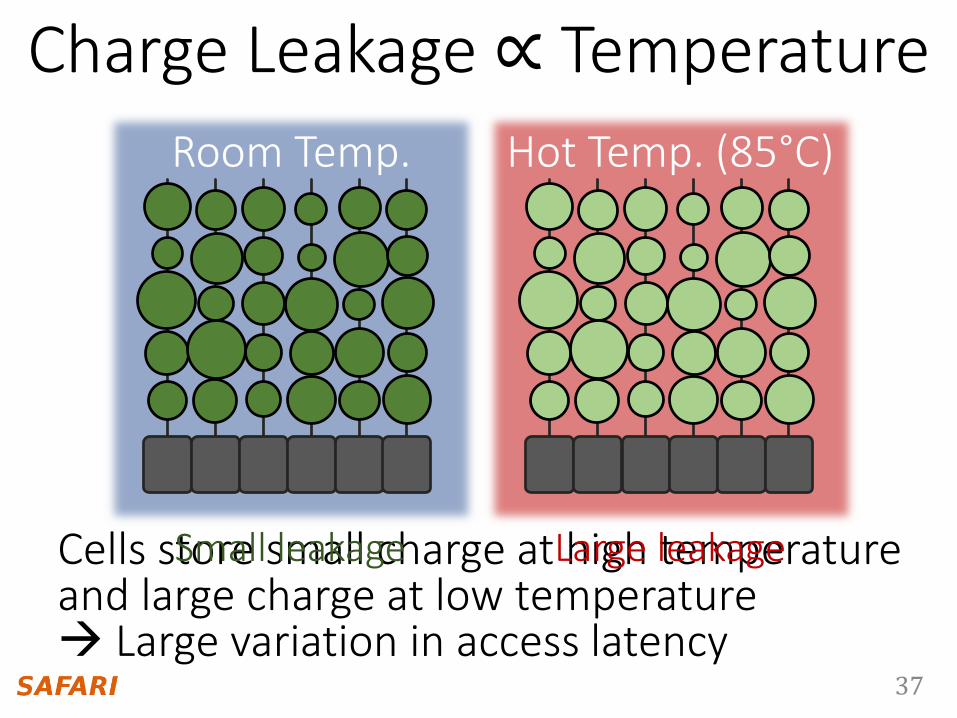
37
Cells store small charge at high temperatureand large charge at low temperature Large variation in access latency
Charge Leakage ∝ Temperature
Room Temp. Hot Temp. (85°C)
Small leakage Large leakage
38
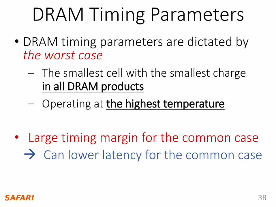
DRAM Timing Parameters• DRAM timing parameters are dictated by
the worst case
– The smallest cell with the smallest charge in all DRAM products
– Operating at the highest temperature
• Large timing margin for the common case
Can lower latency for the common case
39
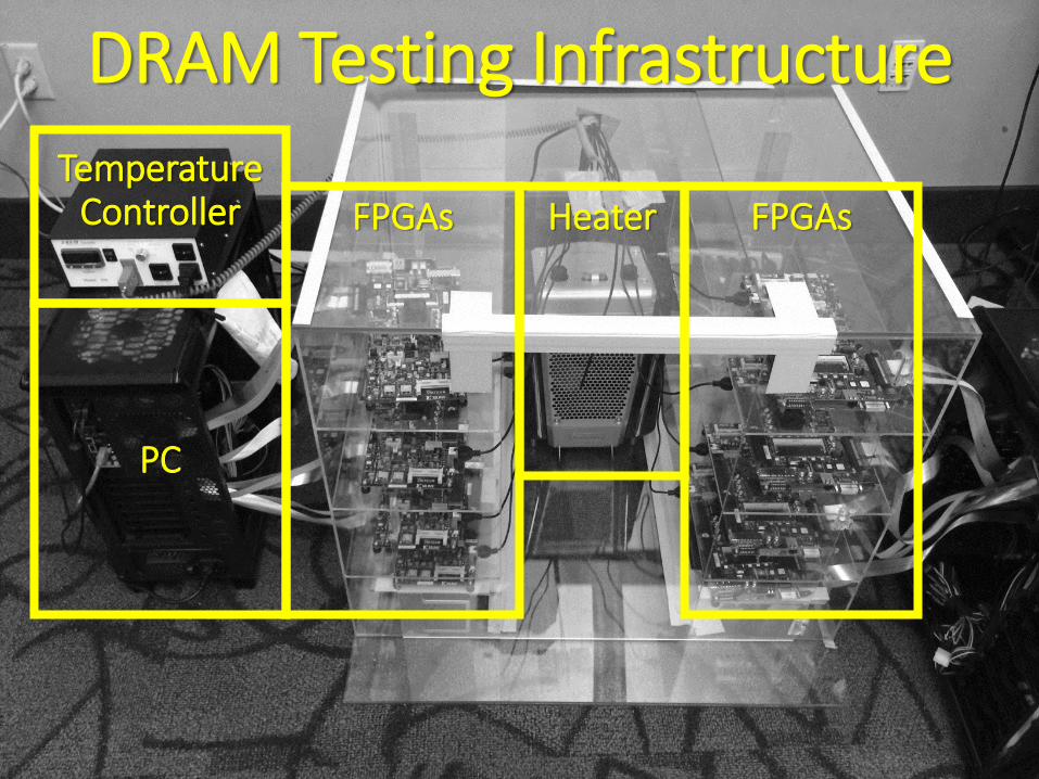
TemperatureController
PC
HeaterFPGAs FPGAs
DRAM Testing Infrastructure
40
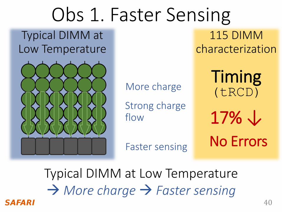
Typical DIMM at Low Temperature
Obs 1. Faster Sensing
More charge
Strong chargeflow
Faster sensing
Typical DIMM at Low TemperatureMore charge Faster sensing
Timing(tRCD)
17% ↓No Errors
115 DIMM characterization
41
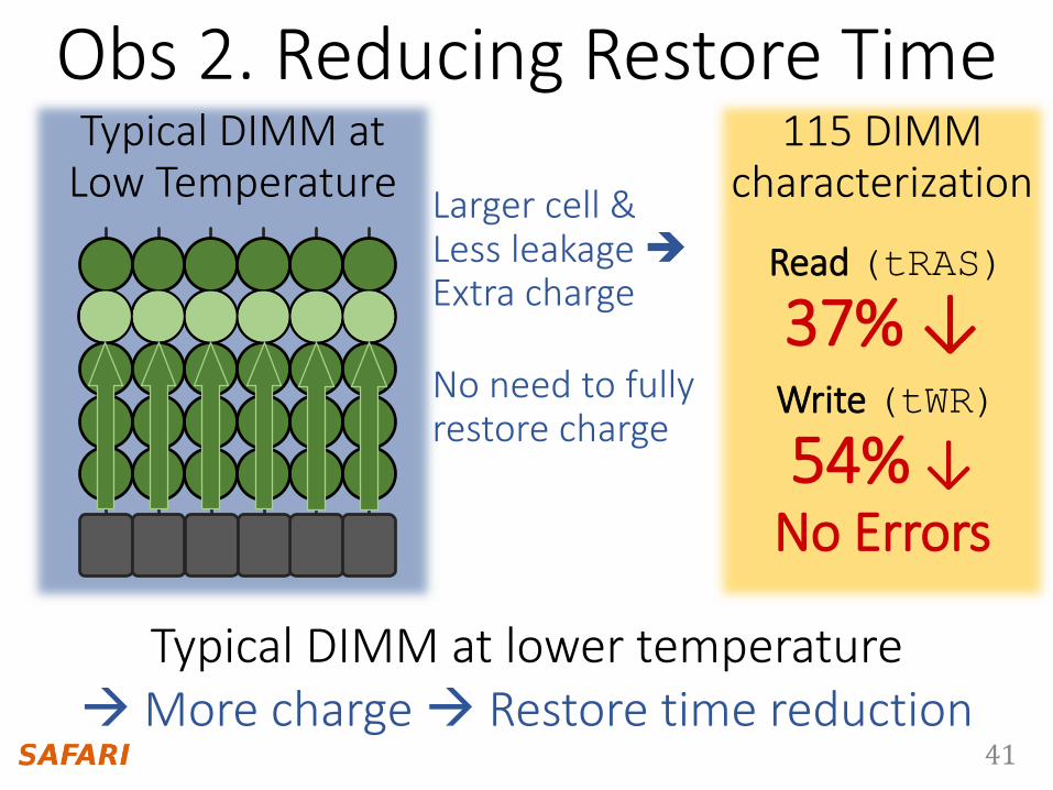
Obs 2. Reducing Restore Time
Larger cell & Less leakage Extra charge
No need to fullyrestore charge
Typical DIMM at lower temperatureMore charge Restore time reduction
Read (tRAS)
37% ↓Write (tWR)
54% ↓No Errors
115 DIMM characterization
Typical DIMM at Low Temperature

42
Empty (0V)
Full (Vdd)
Half
Obs 3. Reducing Precharge Time
Bit
line
Sense amplifier
Sensing Precharge
Precharge ? – Setting bitline to half-full charge
Typical DIMM at Low Temperature

43
Empty (0V) Full (Vdd)
Half
bitline
Not fully precharged
More charge strong sensing
Access empty cell Access full cell
Timing(tRP)
35% ↓No Errors
115 DIMM characterization
Typical DIMM at Lower TemperatureMore charge Precharge time reduction
Obs 3. Reducing Precharge Time

44
Adaptive-Latency DRAM
• Key idea– Optimize DRAM timing parameters online
• Two components– DRAM manufacturer profiles multiple sets of
reliable DRAM timing parameters at different temperatures for each DIMM
– System monitors DRAM temperature & uses appropriate DRAM timing parameters
reliable DRAM timing parameters
DRAM temperature
45
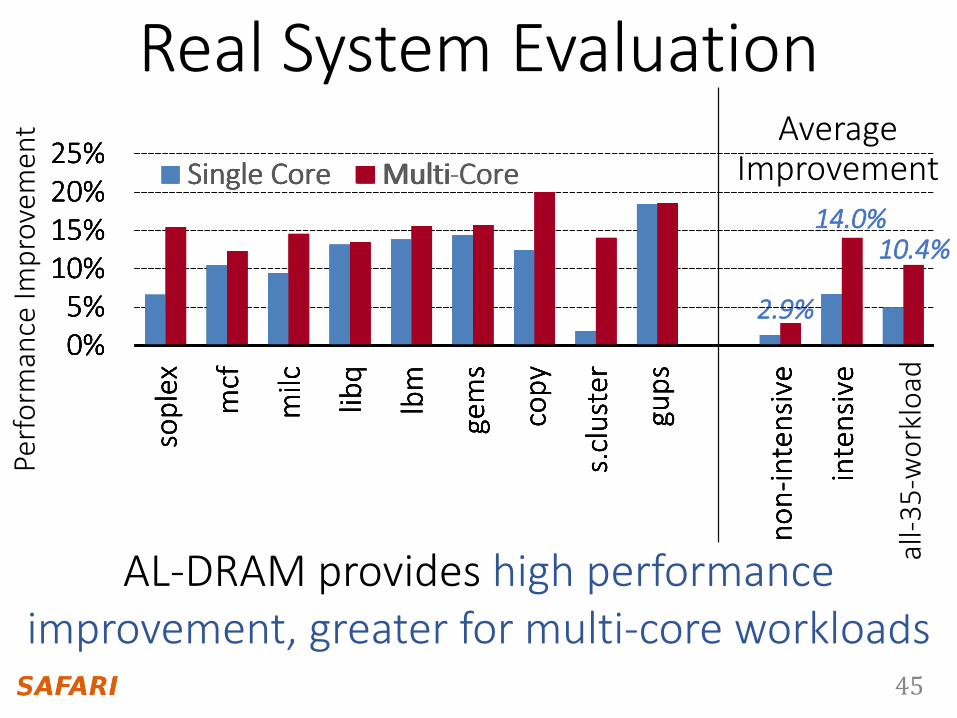
0%5%
10%15%20%25%
sop
lex
mcf
milc
libq
lbm
gem
s
cop
y
s.cl
ust
er
gup
s
no
n-i
nte
nsi
ve
inte
nsi
ve
all-
wo
rklo
ads
Single Core Multi Core
0%5%
10%15%20%25%
sop
lex
mcf
milc
libq
lbm
gem
s
cop
y
s.cl
ust
er
gup
s
no
n-i
nte
nsi
ve
inte
nsi
ve
all-
wo
rklo
ads
Single Core Multi Core
0%5%
10%15%20%25%
sop
lex
mcf
milc
libq
lbm
gem
s
cop
y
s.cl
ust
er
gup
s
no
n-i
nte
nsi
ve
inte
nsi
ve
all-
wo
rklo
ads
Single Core Multi Core
14.0%
2.9%0%5%
10%15%20%25%
sop
lex
mcf
milc
libq
lbm
gem
s
cop
y
s.cl
ust
er
gup
s
no
n-i
nte
nsi
ve
inte
nsi
ve
all-
wo
rklo
ads
Single Core Multi-Core
10.4%
Real System Evaluation
AL-DRAM provides high performance improvement, greater for multi-core workloads
Perf
orm
ance
Imp
rove
men
t Average Improvement
all-
35
-wo
rklo
ad
46
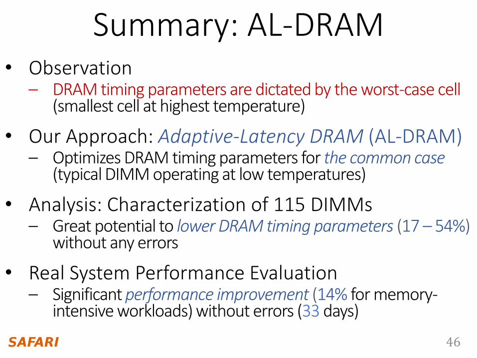
Summary: AL-DRAM• Observation
– DRAM timing parameters are dictated by the worst-case cell (smallest cell at highest temperature)
• Our Approach: Adaptive-Latency DRAM (AL-DRAM) – Optimizes DRAM timing parameters for the common case
(typical DIMM operating at low temperatures)
• Analysis: Characterization of 115 DIMMs– Great potential to lower DRAM timing parameters (17 – 54%)
without any errors
• Real System Performance Evaluation – Significant performance improvement (14% for memory-
intensive workloads) without errors (33 days)

47
AVA-DRAM:Lowering DRAM Latencyby Exploiting Architectural Variation
Approach 3
Lee et al., AVA-DRAM: Reducing DRAM Latency by Exploiting Architectural Variation, under submission
Outline
Prior Work
Future Research Direction
1. TL-DRAM Reducing DRAM Latency by Modifying Bitline Architecture
2. AL-DRAM Optimizing DRAM Latency for the Common-Case
3. AVA-DRAM Lowering DRAM Latencyby Exploiting Architectural Variation
Optimizing DRAM Latency for the Common Case2. AL-DRAM
Lowering DRAM Latencyby Exploiting Architectural Variation3. AVA-DRAM
48
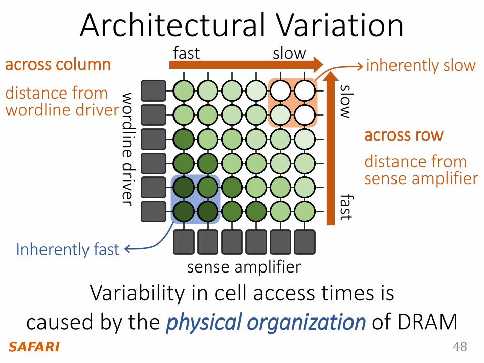
Inherently fast
inherently slow
Architectural Variationslowfast
slow
fast
Variability in cell access times iscaused by the physical organization of DRAM
sense amplifier
wo
rdlin
ed
river
across row
distance from sense amplifier
across column
distance from wordline driver

49
Our Approach
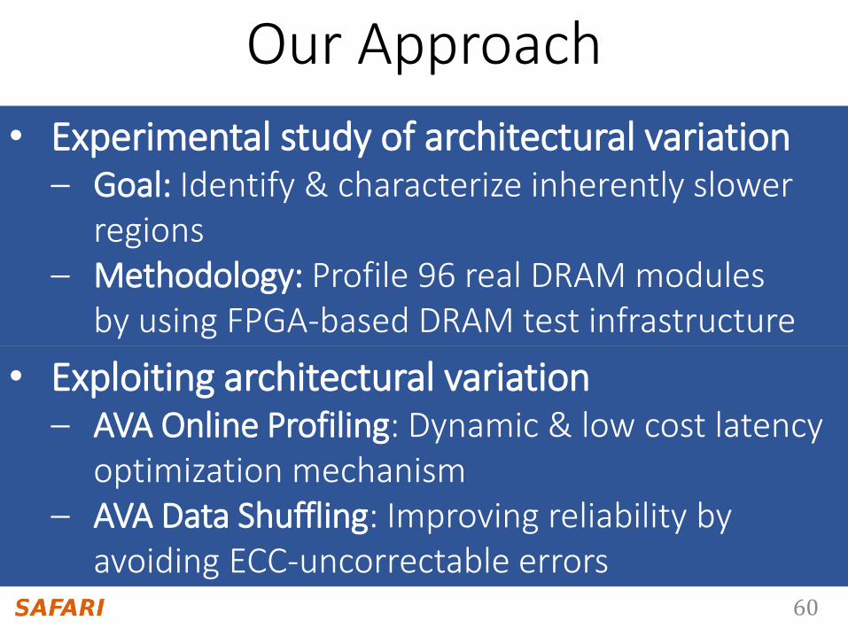
• Experimental study for architectural variation– Goal: Identify & characterize inherently slower
regions – Methodology: Profiling 96 real DRAM modules
by using FPGA-based DRAM test infrastructure
• Exploiting architectural variation – AVA Online Profiling: Dynamic & low cost latency
optimization mechanism– AVA Data Shuffling: Improving reliability by
avoiding ECC-uncorrectable errors
• Experimental study of architectural variation– Goal: Identify & characterize inherently slower
regions – Methodology: Profile 96 real DRAM modules
by using FPGA-based DRAM test infrastructure
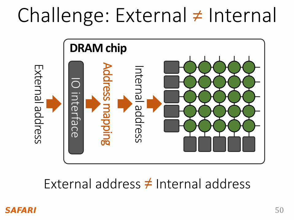
50
Internal address
External address
Challenge: External ≠ Internal
External address ≠ Internal address
DRAM chip
IO in
terface
Address m
apping
51
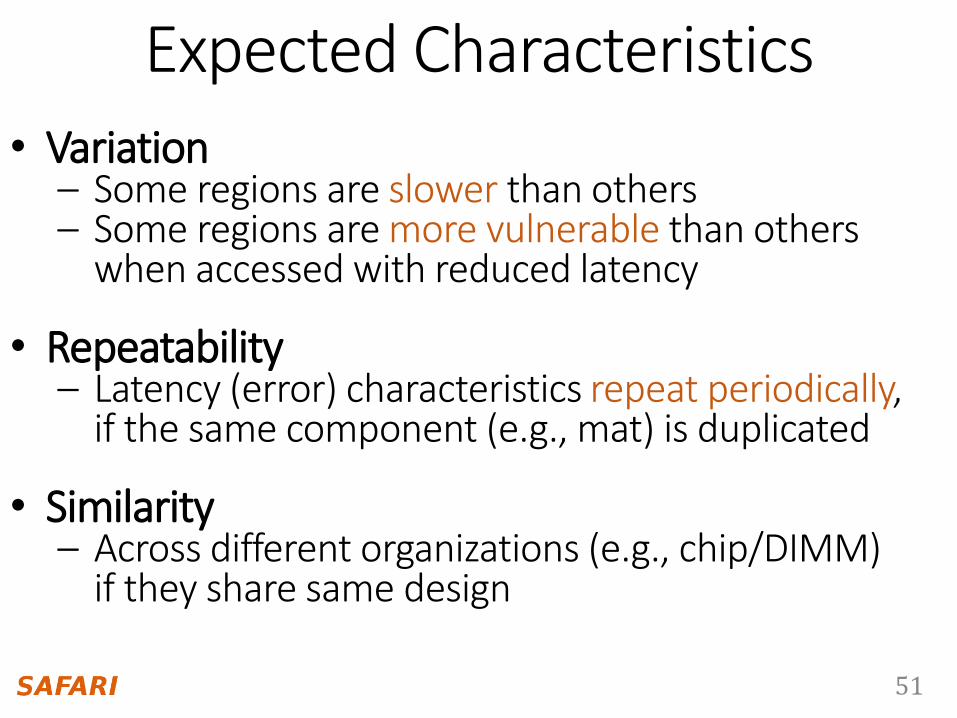
Expected Characteristics
• Variation– Some regions are slower than others– Some regions are more vulnerable than others
when accessed with reduced latency
• Repeatability– Latency (error) characteristics repeat periodically,
if the same component (e.g., mat) is duplicated
• Similarity– Across different organizations (e.g., chip/DIMM)
if they share same design

52
1. Variation & Repeatability in Rows
row
deco
der
512 rows
512 rows
sweep across row
s
Latency characteristics vary across 512 rows
global wordline
row
deco
der
Same organization repeats every 512 rowsLatency characteristics repeat every 512 rows
53
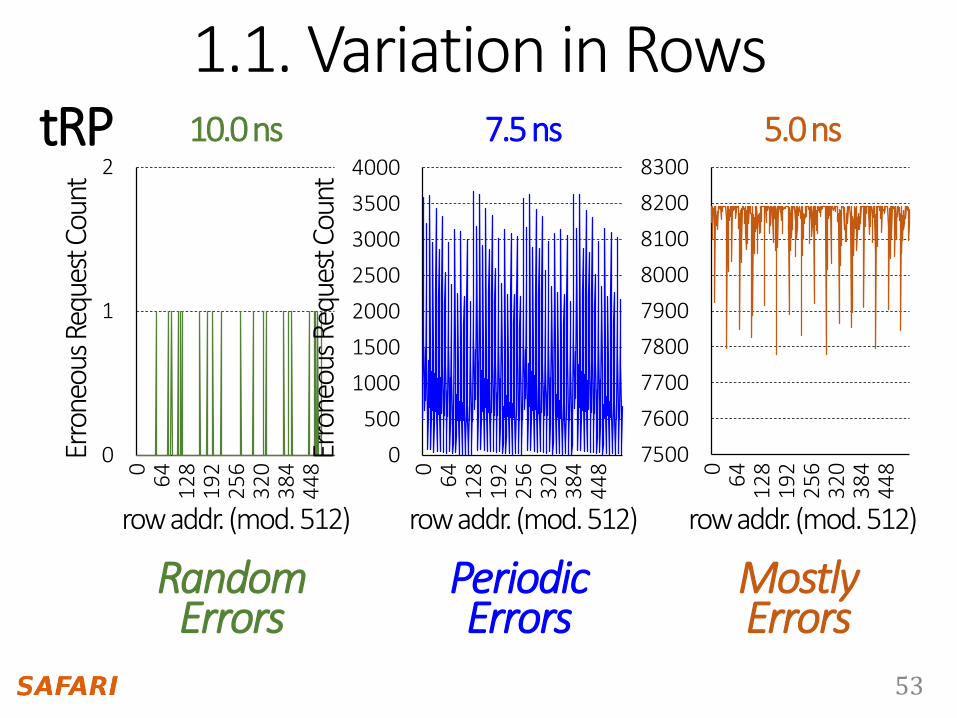
1.1. Variation in Rows
0
500
1000
1500
2000
2500
3000
3500
4000
06
41
28
19
22
56
32
03
84
44
8
0
1
20
64
12
81
92
25
63
20
38
44
48
7500
7600
7700
7800
7900
8000
8100
8200
8300
06
41
28
19
22
56
32
03
84
44
8
row addr. (mod. 512) row addr. (mod. 512) row addr. (mod. 512)
Erro
neou
s Re
ques
t Cou
nt
RandomErrors
PeriodicErrors
MostlyErrors
10.0 ns 7.5 ns 5.0 nstRP
Erro
neou
s Re
ques
t Cou
nt
54
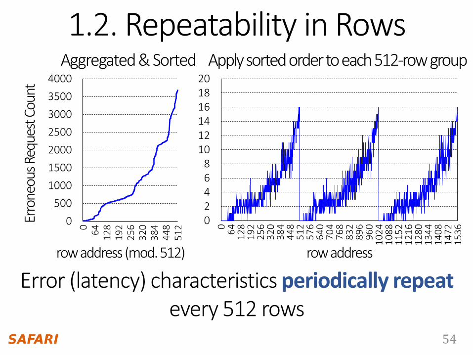
1.2. Repeatability in Rows
0
500
1000
1500
2000
2500
3000
3500
40000
64
12
81
92
25
63
20
38
44
48
51
2
02468
101214161820
06
41
28
19
22
56
32
03
84
44
85
12
57
66
40
70
47
68
83
28
96
96
01
02
41
08
81
15
21
21
61
28
01
34
41
40
81
47
21
53
6
Erro
neou
s Re
ques
t Cou
nt
row address (mod. 512) row address
Aggregated & Sorted Apply sorted order to each 512-row group
Error (latency) characteristics periodically repeat every 512 rows
55
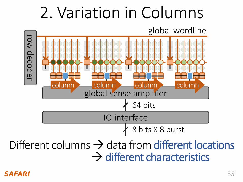
2. Variation in Columns
row
deco
der
IO interface
64 bits
8 bits X 8 burst
global sense amplifiercolumncolumncolumncolumn
Different columns data from different locations different characteristics
global wordline
56
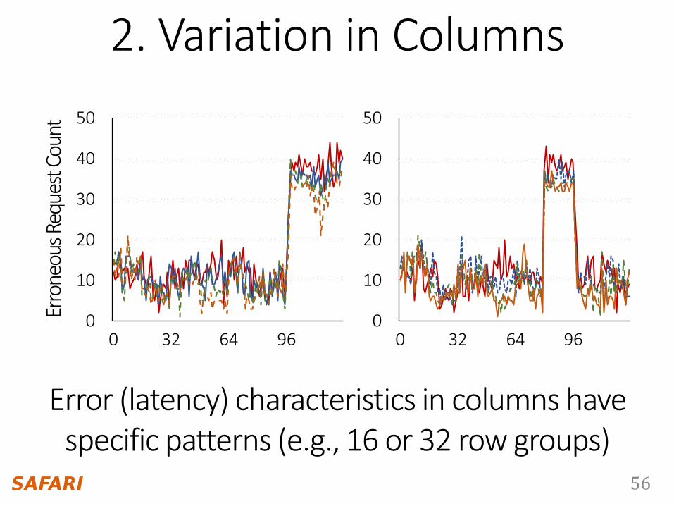
2. Variation in ColumnsEr
rone
ous
Requ
est C
ount
0
10
20
30
40
50
0 32 64 960
10
20
30
40
50
0 32 64 96
Error (latency) characteristics in columns have specific patterns (e.g., 16 or 32 row groups)

57
3. Variation in Data Bits
row
deco
der
IO interface
64 bits
8 bits X 8 burst
global sense amplifier
Data in a request transferred as multiple data bursts
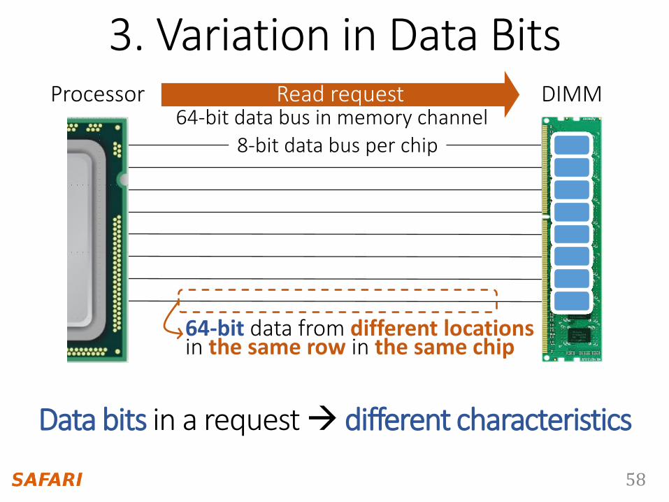
58
8-bit data bus per chip64-bit data bus in memory channel
Processor DIMMRead request
3. Variation in Data Bits
64-bit data from different locations in the same row in the same chip
Data bits in a request different characteristics
59
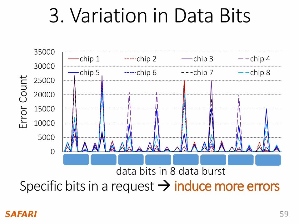
3. Variation in Data Bits
0
5000
10000
15000
20000
25000
30000
35000
0 8 16 24 32 40 48 56
chip 1 chip 2 chip 3 chip 4
chip 5 chip 6 chip 7 chip 8
Erro
r C
ou
nt
data bits in 8 data burst
Specific bits in a request induce more errors
60
• Exploiting architectural variation – AVA Online Profiling: Dynamic & low cost latency
optimization mechanism– AVA Data Shuffling: Improving reliability by
avoiding ECC uncorrectable errors
Our Approach
• Experimental study for architectural variation– Goal: Identify & characterize inherently slower
regions – Methodology: Profiling 96 real DRAM modules
by using FPGA-based DRAM test infrastructure
• Experimental study of architectural variation– Goal: Identify & characterize inherently slower
regions – Methodology: Profile 96 real DRAM modules
by using FPGA-based DRAM test infrastructure
• Exploiting architectural variation – AVA Online Profiling: Dynamic & low cost latency
optimization mechanism– AVA Data Shuffling: Improving reliability by
avoiding ECC-uncorrectable errors
61
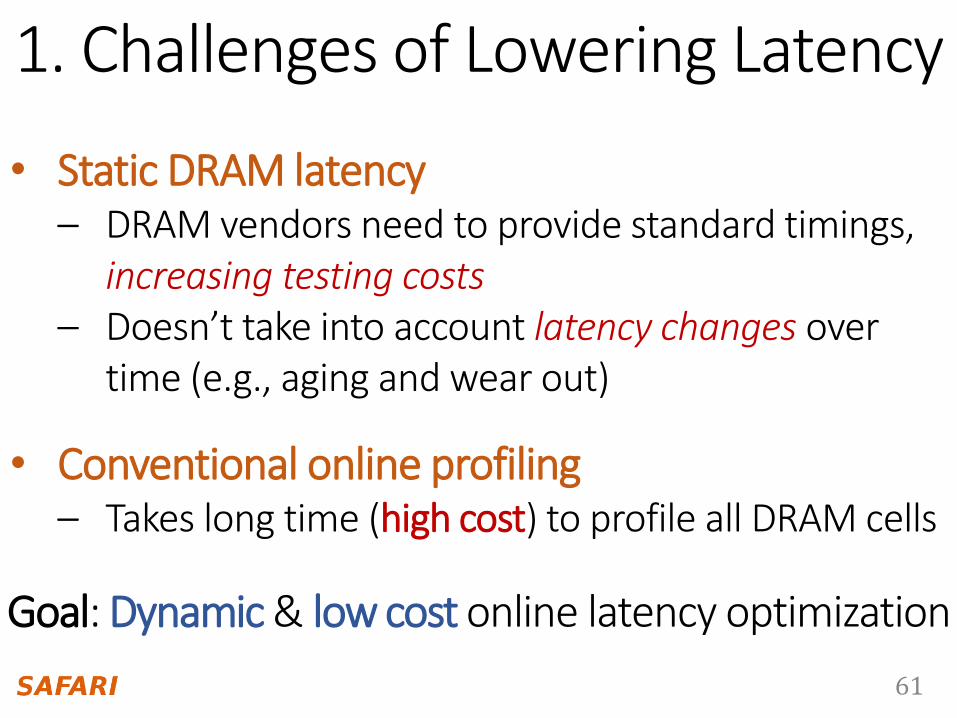
1. Challenges of Lowering Latency
• Static DRAM latency– DRAM vendors need to provide standard timings,
increasing testing costs– Doesn’t take into account latency changes over
time (e.g., aging and wear out)
• Conventional online profiling– Takes long time (high cost) to profile all DRAM cells
Goal: Dynamic & low cost online latency optimization
62
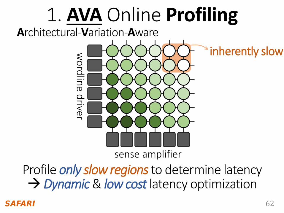
1. AVA Online Profiling
inherently slow
Profile only slow regions to determine latencyDynamic & low cost latency optimization
sense amplifier
wo
rdlin
ed
river
Architectural-Variation-Aware

63
inherently slow
1. AVA Online Profiling
slow cells
architecturalvariation
processvariation
localized errorrandom error
online profilingerror-correcting code
Combining error-correcting code & online profiling Reliably reduce DRAM latency
Architectural-Variation-Aware
sense amplifier
wo
rdlin
ed
river
64
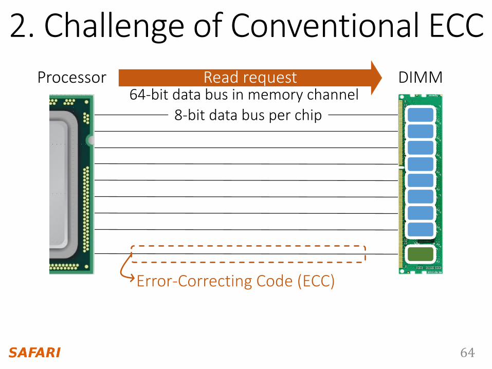
8-bit data bus per chip64-bit data bus in memory channel
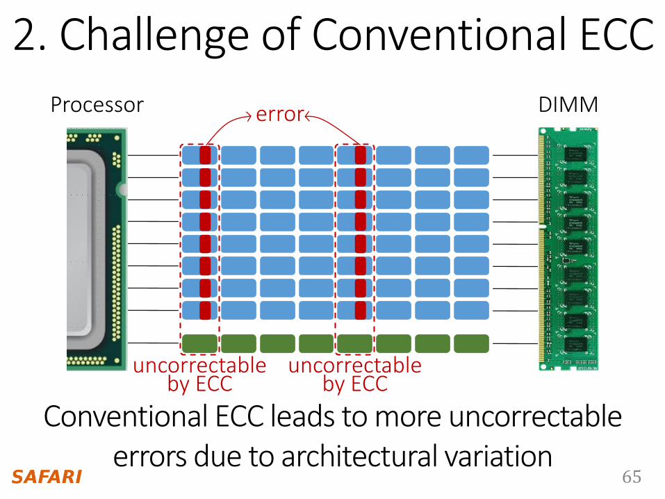
2. Challenge of Conventional ECCProcessor DIMMRead request
Error-Correcting Code (ECC)
65
8-bit data bus per chip
Processor DIMMerror
uncorrectable by ECC
uncorrectable by ECC
Conventional ECC leads to more uncorrectable errors due to architectural variation
2. Challenge of Conventional ECC
66
8-bit data bus per chip
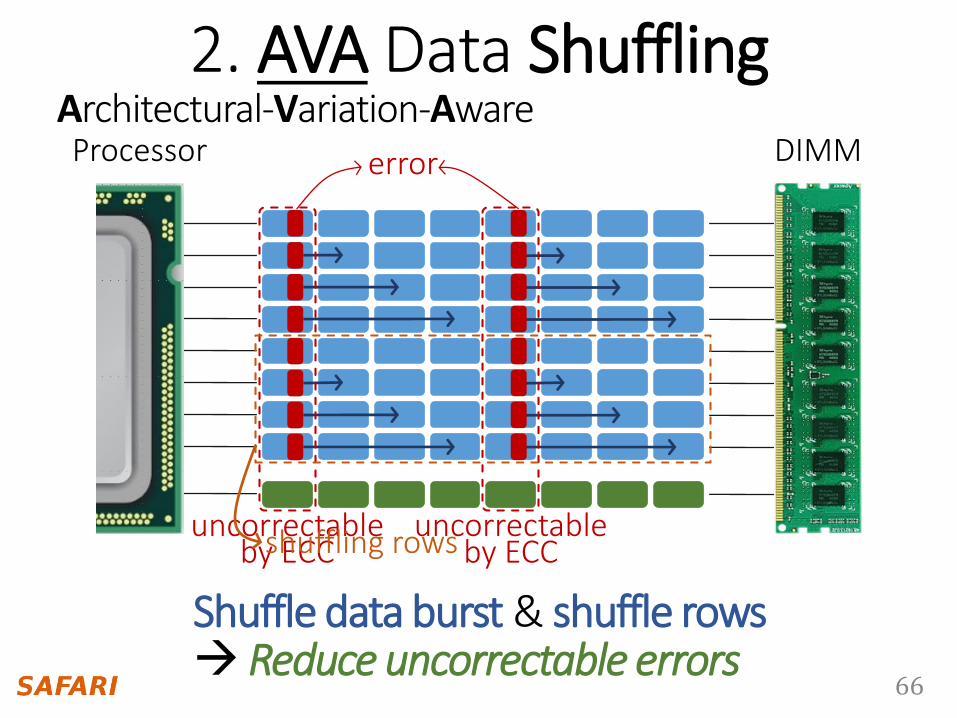
2. AVA Data ShufflingProcessor DIMMerror
uncorrectable by ECC
uncorrectable by ECC
Shuffle data burst & shuffle rows Reduce uncorrectable errors
shuffling rows
Architectural-Variation-Aware
67
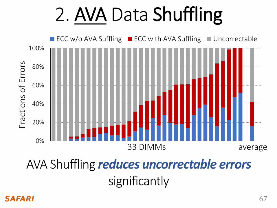
2. AVA Data Shuffling
0%
20%
40%
60%
80%
100%
1 2 3 4 5 6 7 8 9 10 11 12 13 14 15 16 17 18 19 20 21 22 23 24 25 26 27 28 29 30 31 32 33 34 35 36
ECC w/o AVA Suffling ECC with AVA Suffling Uncorrectable
AVA Shuffling reduces uncorrectable errors significantly
0%
20%
40%
60%
80%
100%
1 2 3 4 5 6 7 8 9 10 11 12 13 14 15 16 17 18 19 20 21 22 23 24 25 26 27 28 29 30 31 32 33 34 35 36
ECC w/o AVA Suffling ECC with AVA Suffling Uncorrectable
33 DIMMs average
Frac
tio
ns
of
Erro
rs
68
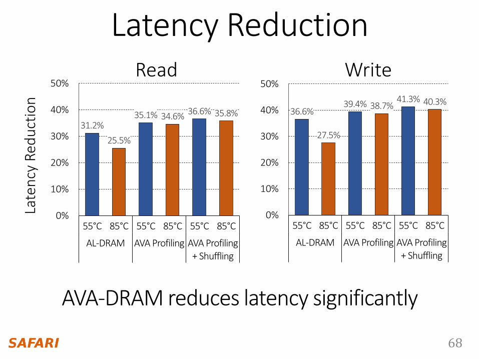
Latency Reduction
AVA-DRAM reduces latency significantly
Read Write
31.2%
25.5%
35.1% 34.6%36.6% 35.8%
0%
10%
20%
30%
40%
50%
55°C 85°C 55°C 85°C 55°C 85°C
AL-DRAM AVA Profiling AVA Profiling + Shuffling
36.6%
27.5%
39.4% 38.7%41.3% 40.3%
0%
10%
20%
30%
40%
50%
55°C 85°C 55°C 85°C 55°C 85°C
AL-DRAM AVA Profiling AVA Profiling + Shuffling
Late
ncy
Red
uct
ion
69
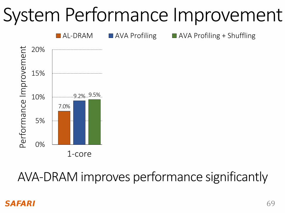
System Performance Improvement
7.0%
11.7% 11.0% 11.5%
9.2%
14.7%13.7% 13.8%
9.5%
15.1%14.2% 14.1%
0%
5%
10%
15%
20%
1-core 2-core 4-core 8-core
AL-DRAM AVA Profiling AVA Profiling + Shuffling
Perf
orm
ance
Imp
rove
men
t
AVA-DRAM improves performance significantly
70
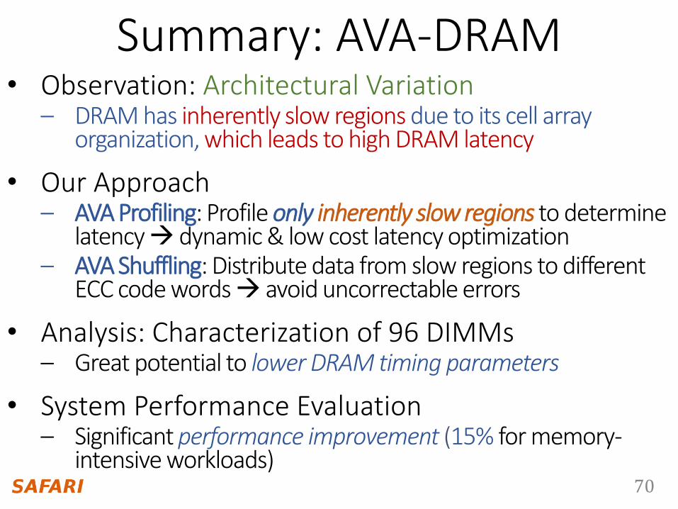
Summary: AVA-DRAM• Observation: Architectural Variation
– DRAM has inherently slow regions due to its cell array organization, which leads to high DRAM latency
• Our Approach– AVA Profiling: Profile only inherently slow regions to determine
latency dynamic & low cost latency optimization– AVA Shuffling: Distribute data from slow regions to different
ECC code words avoid uncorrectable errors
• Analysis: Characterization of 96 DIMMs– Great potential to lower DRAM timing parameters
• System Performance Evaluation – Significant performance improvement (15% for memory-
intensive workloads)

71
Outline
Prior Work
Future Research Direction
1. TL-DRAM Reducing DRAM Latency by Modifying Bitline Architecture
2. AL-DRAM Optimizing DRAM Latency for the Common Case
3. AVA-DRAM Lowering DRAM Latencyby Exploiting Architectural VariationLowering DRAM Latencyby Exploiting Architectural Variation3. AVA-DRAM
Prior Work
72
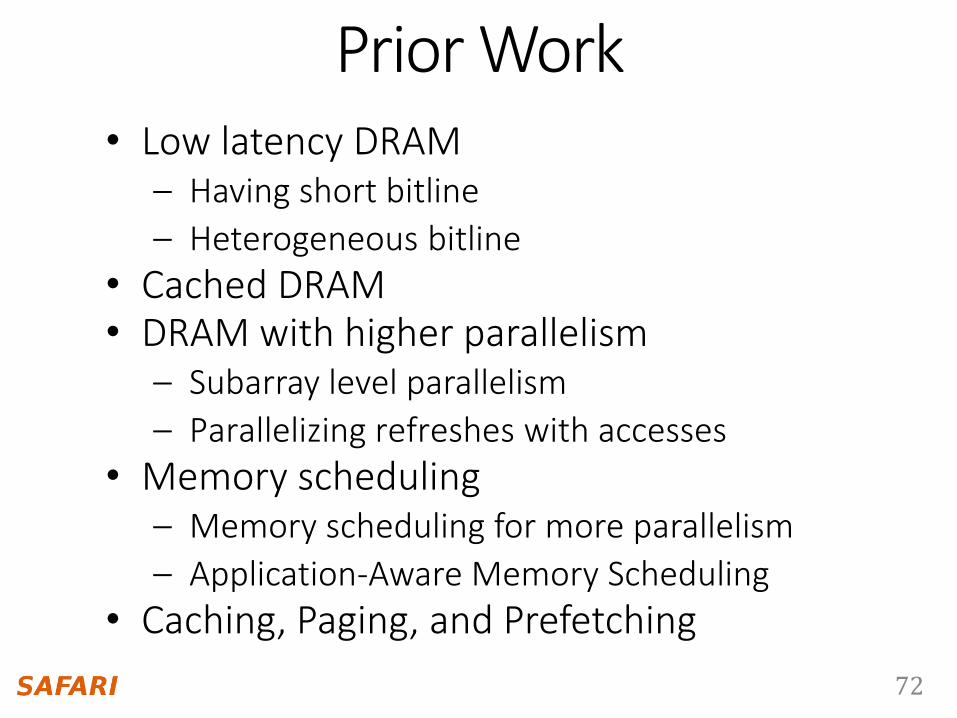
Prior Work• Low latency DRAM
– Having short bitline
– Heterogeneous bitline
• Cached DRAM• DRAM with higher parallelism
– Subarray level parallelism
– Parallelizing refreshes with accesses
• Memory scheduling– Memory scheduling for more parallelism
– Application-Aware Memory Scheduling
• Caching, Paging, and Prefetching
73
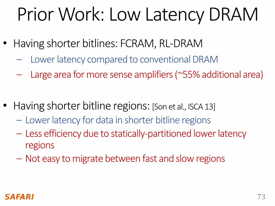
Prior Work: Low Latency DRAM
• Having shorter bitlines: FCRAM, RL-DRAM
– Lower latency compared to conventional DRAM
– Large area for more sense amplifiers (~55% additional area)
• Having shorter bitline regions: [Son et al., ISCA 13]
– Lower latency for data in shorter bitline regions
– Less efficiency due to statically-partitioned lower latency regions
– Not easy to migrate between fast and slow regions
74
Prior Work: Cached DRAM
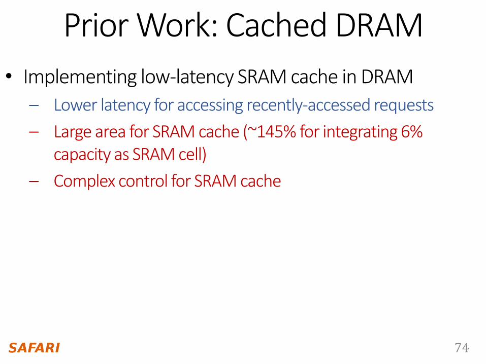
• Implementing low-latency SRAM cache in DRAM
– Lower latency for accessing recently-accessed requests
– Large area for SRAM cache (~145% for integrating 6% capacity as SRAM cell)
– Complex control for SRAM cache
75
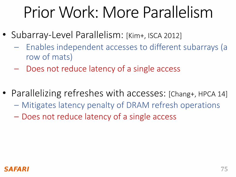
Prior Work: More Parallelism• Subarray-Level Parallelism: [Kim+, ISCA 2012]
– Enables independent accesses to different subarrays (a row of mats)
– Does not reduce latency of a single access
• Parallelizing refreshes with accesses: [Chang+, HPCA 14]
– Mitigates latency penalty of DRAM refresh operations
– Does not reduce latency of a single access
76
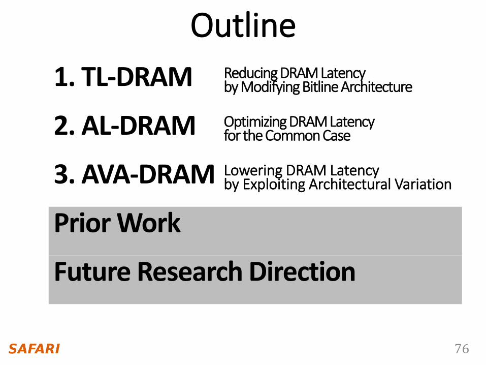
Outline
Prior Work
Future Research Direction
1. TL-DRAM Reducing DRAM Latency by Modifying Bitline Architecture
2. AL-DRAM Optimizing DRAM Latency for the Common Case
3. AVA-DRAM Lowering DRAM Latencyby Exploiting Architectural Variation
Prior Work
Future Research Direction
77
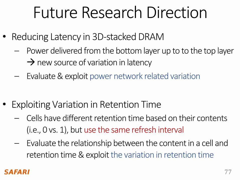
Future Research Direction• Reducing Latency in 3D-stacked DRAM
– Power delivered from the bottom layer up to to the top layer
new source of variation in latency
– Evaluate & exploit power network related variation
• Exploiting Variation in Retention Time– Cells have different retention time based on their contents
(i.e., 0 vs. 1), but use the same refresh interval
– Evaluate the relationship between the content in a cell and retention time & exploit the variation in retention time
78
Future Research Direction
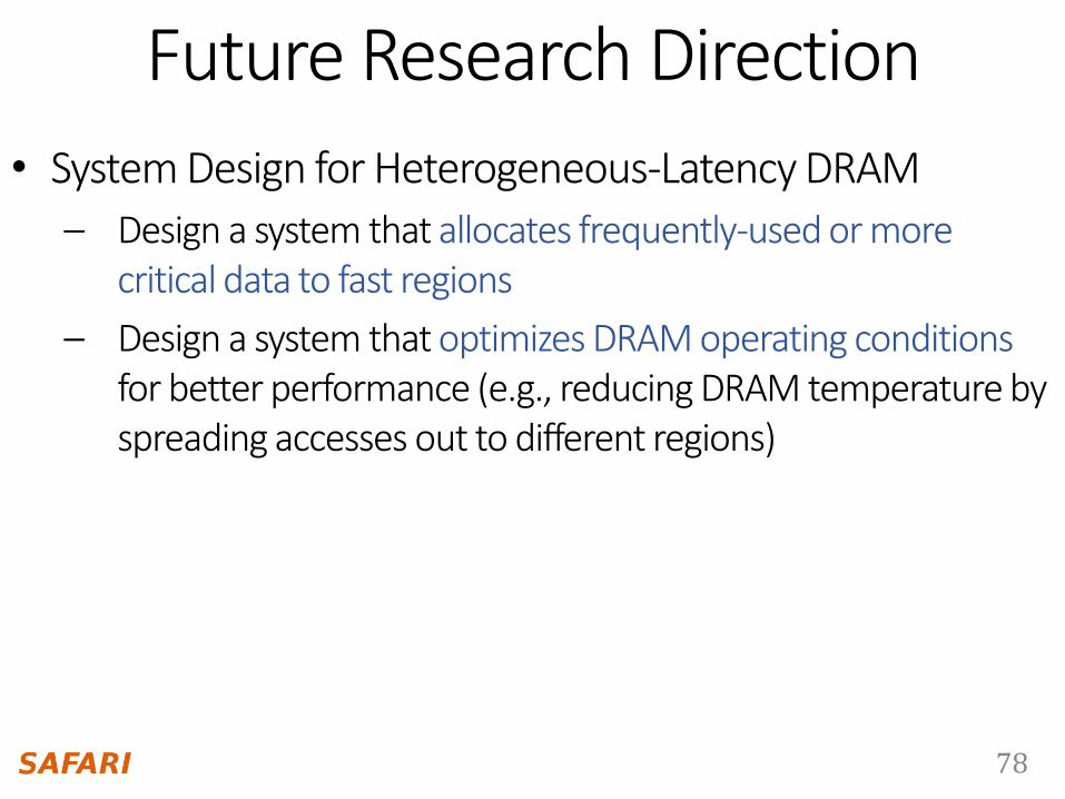
• System Design for Heterogeneous-Latency DRAM
– Design a system that allocates frequently-used or more critical data to fast regions
– Design a system that optimizes DRAM operating conditions for better performance (e.g., reducing DRAM temperature by spreading accesses out to different regions)

79
Conclusion• Observation
– DRAM cell array is the dominant source of high latency
• DRAM latency can be reduced by enabling and exploiting latency heterogeneity
• Our Three Approaches– TL-DRAM: Enabling latency heterogeneity
by changing DRAM architecture– AL-DRAM: Exploiting latency heterogeneity
from process variation and temperature dependency– AVA-DRAM: Exploiting latency heterogeneity
from architectural variation
• Evaluation & Result– Our mechanisms enable significant latency reduction
at low cost and thus improve system performance
80
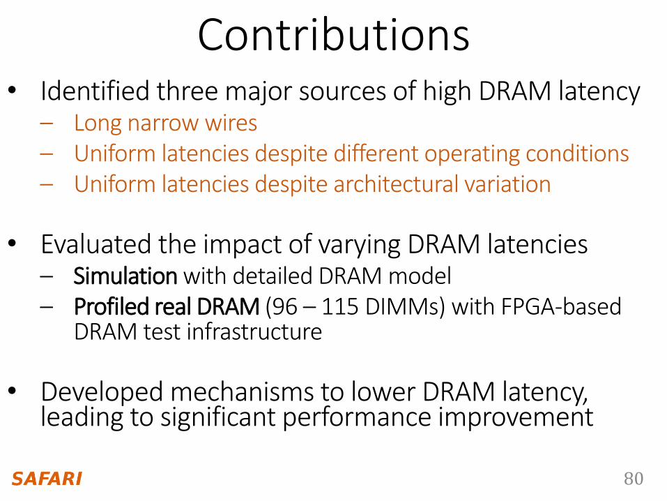
Contributions• Identified three major sources of high DRAM latency
– Long narrow wires– Uniform latencies despite different operating conditions– Uniform latencies despite architectural variation
• Evaluated the impact of varying DRAM latencies– Simulation with detailed DRAM model– Profiled real DRAM (96 – 115 DIMMs) with FPGA-based
DRAM test infrastructure
• Developed mechanisms to lower DRAM latency, leading to significant performance improvement

Reducing DRAM Latency at Low Cost by Exploiting Heterogeneity
Donghyuk Lee
Carnegie Mellon University