Reconfigurable Wave Velocity Transmission Lines … Wave Velocity Transmission Lines for Phased...
18
Reconfigurable Wave Velocity Transmission Lines for Phased Arrays Advisors: Chi-Chih Chen John L. Volakis 1 By: Nicholas Host NASA Mentor: Félix Miranda Work supported by NSTRF, NASA Grant #NNX11AN16H https://ntrs.nasa.gov/search.jsp?R=20120015258 2018-07-01T21:48:33+00:00Z
Transcript of Reconfigurable Wave Velocity Transmission Lines … Wave Velocity Transmission Lines for Phased...

Reconfigurable Wave Velocity TransmissionLines for Phased Arrays
Advisors: Chi-Chih Chen John L. Volakis
1
By: Nicholas Host
NASA Mentor: Félix MirandaWork supported by NSTRF, NASA Grant #NNX11AN16H
https://ntrs.nasa.gov/search.jsp?R=20120015258 2018-07-01T21:48:33+00:00Z
2
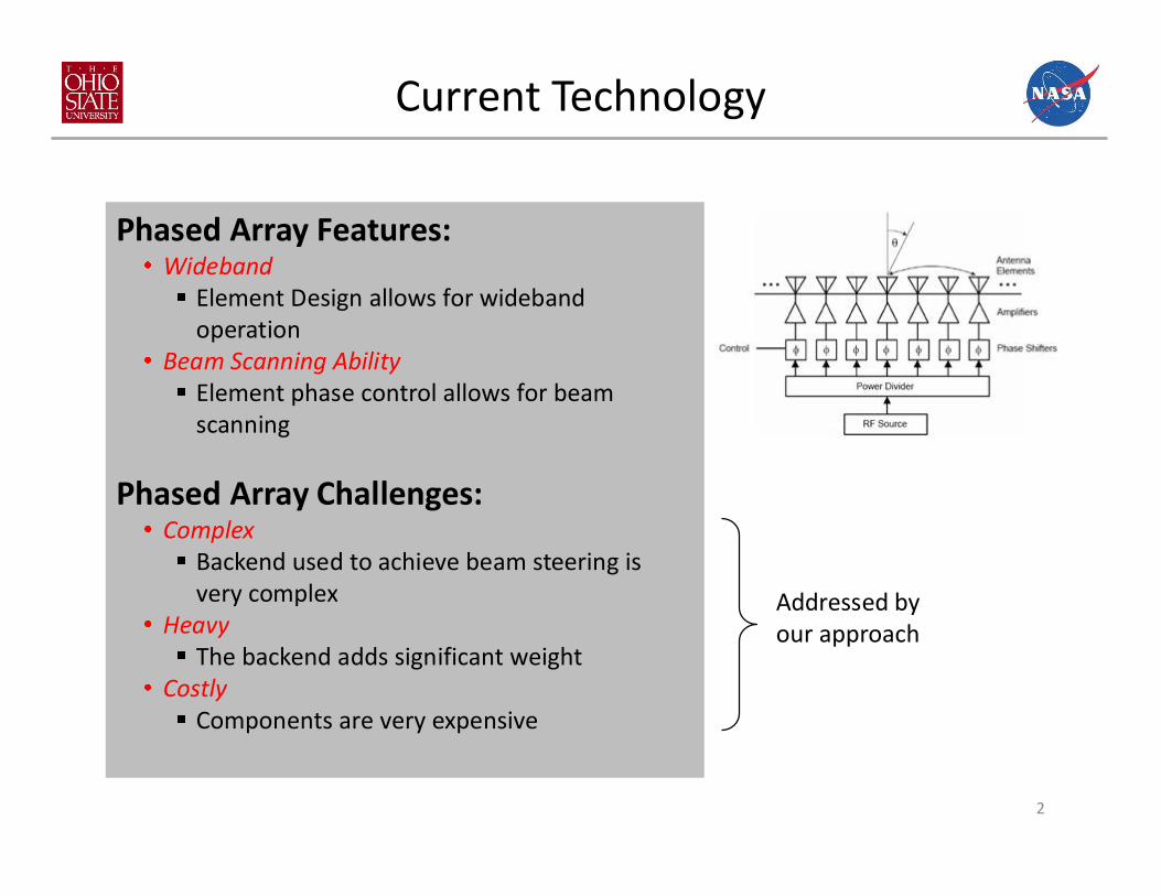
Current Technology
Phased Array Features:Wideband
Element Design allows for widebandoperation
Beam Scanning AbilityElement phase control allows for beamscanning
Phased Array Challenges:Complex
Backend used to achieve beam steering isvery complex
HeavyThe backend adds significant weight
CostlyComponents are very expensive
Addressed byour approach

3
Novel Aspects
Design Goals:Reduce ComplexityReduce Weight
Large contributions for both come from thebackend
Reduce Cost
Methodology:Replace backend with simpler feeding mechanism
Replace withsimplermechanism

4
Approach
Replace Backend With SimplerMechanism
Get rid of all splitters, phase shifters, and ampsUse Series Fed Array:
Array fed at one point (side)Magnitude at each element controlled by variedmismatch at element terminalsBeam Steering will be accomplished by acontrollable propagation constant betweenelements
A motor can bring two fixed sheets closer tochange the effective dielectric constant
Varied
Motor to movesheets closer or
farther apart
Field mostly inair, so low eff
Field mostly indielectric, so high eff
By changing (through change of keff) scanning is accomplished:
Reconfigurable transmission line

5
Achieving Scanning
Move platescloser
Scanning is achieved with one mechanical motion and no phase shifters

k eff /
k 0• Needed Transmission Line Agility
Assume each transmission line is the same Scan Angle
d )
d >< ~ Zg < ~ cU Z, Z2 ryo, k'ff Z3 rlo, k eff
••• JZn • -t • 2¢
• ¢
• • • 3¢ 4¢
¢ = ted, keff )
~----=ec=-~£t J For d = 0.4;1 and 11>_ uu~ keff -+ e = 0°
-=5 41--------------f!'..
2
O~I ----~--------~--------~--------~
0.2 0.3 0.4 0.5 Element Spacing, d (*A)
ko
For e = -60 to 60 at d = 0.25;1 -+
Need k
3.1 < ~~f < 4.9
•
• n¢
6

7
Process to Scan
Theoretical 10Element array with
element spacing
As the parallel plates close (left) (right top)
For givenScan angle (right top)Pattern (right bottom)
k eff /
k 0
k eff /
k 0

9
Array as a Circuit Network
Equal Power Distribution Power at the
element
Uniform patternMatching at Feed
minimized at Feed
Feed ( )

10
General Impedance Distribution Elements
So:
knowing:
Equal Power Distribution Circuit Matching
To be matched:Valid for all
Or:

11
Analytical Formulation of
Equal Power Distribution Condition:
In This Case:
So:
1
For Equal PowerDistribution
Element Element
Use same antenna element
Derivation Graphical Representation
Not dependent on

Impe
danc
e of
Lin
e (
)
k eff /
k 0k ef
f / k 0
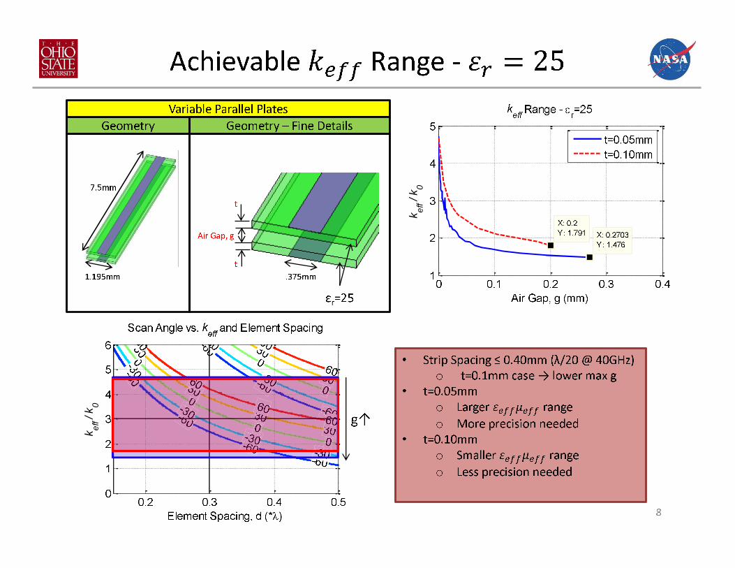
• Transmission Line Attributes • 4
~} 3
2
1
O~I --~~------~--------~--------~
0.2 0.3 0.4 0.5 Element Spacing, d (*A)
k ff Range - E =25 e r
5c~------.-------~------~------~
4
X: 0.001524 Y: 4.078
AirGan~~
3 f-.U-----------+-----------'-f
2
10
-------+.-----------1--- Chaos e -.. -.--... --.-.. ----J. '"'" i I
0.001524 < 9 < 0.042
0.1 0.2 0.3 0.4 Air Gap, g (mm)
A d=-
2
k ---+ Can scan to all angles 2 < eff < 4
- ko -
Impedance of Line 140~c------~----~~----~------~
120 t-------------------L----------J--- ---1---------c I!! 1 00 ------------------r-------- -r---------+---------
. I I 80 f---------------------i ------------r--------- ! ---------
x: 0.042 : 1 y. 5233 : : 60 r-------; ,. · . j-----------r------------L----------
4°1f--1----+-1 ZO_de~~:nose 32[1 . 20·-----------------t------------c------------'----------l x: 0.001524 I I I o Y: 19.23 o J.1 0.2 0.3 0.4
Air Gap, g (mm) 12

13
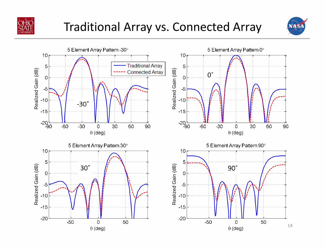
Simulation of Connected Array
Separate plates tofacilitate scanning
Gap
3.75
Z=22
Z0
.375
.05
Gap.05
1.2
*All labels in mm
@ 40GHz = 7.5mm
Z=42
Thickness=0.05
Rea
lized
Gai
n (d
B)
Rea
lized
Gai
n (d
B)
14
Traditional Array vs. Connected ArrayR
ealiz
ed G
ain
(dB
)
Rea
lized
Gai
n (d
B)
-
3 9

15
22 Element Prototype Design
Rea
lized
Gai
n (d
B)
RT6002R03010
60mil
60mil
10mil
g
Practical Transmission Line DesignCircuit printed on two 60mil thick RT6002 boards
o RO3010 becomes ripply when unsupportedRO3010 material bonded to inside of one of boards
g=0.73mil g=9mil

16
Assembly of Prototype
Pinch togethertwo boards with
metal frames
Fit top dielectricon with shims as
spacers
Alignment PinsTightening Bolts
CompressingFrame
Top Dielectric
Bottom Dielectric
Spacing Shims
17
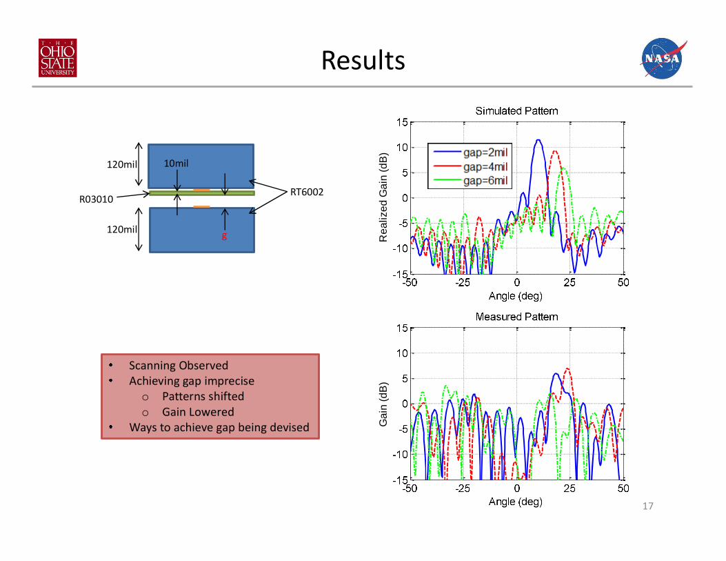
Results
RT6002R03010
120mil
120mil
10mil
g Rea
lized
Gai
n (d
B)
Gai
n (d
B)
Scanning ObservedAchieving gap impreciseo Patterns shiftedo Gain Lowered
Ways to achieve gap being devised

18
Future Work
2-D ScanningOne feedIndependent control of each scanning axis
Hard with current transmission line
Transmission Line DesignIndependent control of
Wave VelocityImpedance