Reconfigurable Computing for Spacecdn.intechweb.org/pdfs/6834.pdf · Reconfigurable Computing for...
15
3 Reconfigurable Computing for Space Donohoe, Gregory W. 1 and Lyke, James C. 2 1 University of Idaho 2 Air Force Research Laboratory USA 1. Introduction Reconfigurable computing is an emerging technology with important implications for space systems. Spacecraft serve as sensor platforms to gather, format, possibly screen or interpret, and then downlink sensor data. Once launched, a spacecraft may operate unattended for decades. The trend in spacecraft design is toward more complex and voluminous data, including multispectral and hyperspectral images and synthetic aperture radar, which require extensive on-board data processing. Other on-board computing tasks are navigation, orientation, and communication. As spacecraft grow more sophisticated, the need for higher-performance computing grows also. Reconfigurable computing allows computing hardware to be configured or “wired” by software to optimize the architecture for the problem at hand. Some early discussions of reconfigurable computing are found in (DeHon, 1996), and Villasenor (Villasenor, 1997). Reconfigurable computers may be implemented on specially-designed hardware, or on Field Programmable Gate Arrays (FPGAs). Hauck and DeHon cover FPGA-based reconfigurable computing very thoroughly their book (Hauck, 2008). The space environment presents special challenges to the system designer. Chief among these are: 1. Power efficiency. Electrical power is a scarce and expensive commodity for orbiters and deep space probes. In addition, removing heat generated by electronics is very challenging in space, where air cooling is not an option. 2. Minimum size and weight. Increased size and weight increase launch costs, and require more fuel for on-orbit maneuvering. 3. High reliability for long mission life. On-orbit repair is rarely feasible, and the time and monetary cost of replacing a spacecraft are high. 4. Rapid deployment or redeployment of spacecraft to meet new or changing mission requirements. 5. Radiation tolerance. The specific requirements depend on the mission profile, but all spacecraft systems must be designed to cope with cosmic radiation, chiefly heavy ions. In some space missions, rapid deployment of a new spacecraft, or redeployment of an existing craft, are of high priority. Many of potential benefits of reconfigurability for space are laid out in (Lanza, 2004). Reconfigurability can help designers meet challenges (1) and (2) above by enabling hardware to be reconfigured for different phases of a computational task, resulting in smaller size, lower weight, and reduced power consumption than would Source: Aerospace Technologies Advancements, Book edited by: Dr. Thawar T. Arif, ISBN 978-953-7619-96-1, pp. 492, January 2010, INTECH, Croatia, downloaded from SCIYO.COM www.intechopen.com
Transcript of Reconfigurable Computing for Spacecdn.intechweb.org/pdfs/6834.pdf · Reconfigurable Computing for...

3
Reconfigurable Computing for Space
Donohoe, Gregory W.1 and Lyke, James C.2 1University of Idaho
2Air Force Research Laboratory USA
1. Introduction
Reconfigurable computing is an emerging technology with important implications for space
systems. Spacecraft serve as sensor platforms to gather, format, possibly screen or interpret,
and then downlink sensor data. Once launched, a spacecraft may operate unattended for
decades. The trend in spacecraft design is toward more complex and voluminous data,
including multispectral and hyperspectral images and synthetic aperture radar, which
require extensive on-board data processing. Other on-board computing tasks are navigation,
orientation, and communication. As spacecraft grow more sophisticated, the need for
higher-performance computing grows also.
Reconfigurable computing allows computing hardware to be configured or “wired” by software to optimize the architecture for the problem at hand. Some early discussions of reconfigurable computing are found in (DeHon, 1996), and Villasenor (Villasenor, 1997). Reconfigurable computers may be implemented on specially-designed hardware, or on Field Programmable Gate Arrays (FPGAs). Hauck and DeHon cover FPGA-based reconfigurable computing very thoroughly their book (Hauck, 2008). The space environment presents special challenges to the system designer. Chief among
these are:
1. Power efficiency. Electrical power is a scarce and expensive commodity for orbiters and deep space probes. In addition, removing heat generated by electronics is very challenging in space, where air cooling is not an option.
2. Minimum size and weight. Increased size and weight increase launch costs, and require more fuel for on-orbit maneuvering.
3. High reliability for long mission life. On-orbit repair is rarely feasible, and the time and monetary cost of replacing a spacecraft are high.
4. Rapid deployment or redeployment of spacecraft to meet new or changing mission requirements.
5. Radiation tolerance. The specific requirements depend on the mission profile, but all spacecraft systems must be designed to cope with cosmic radiation, chiefly heavy ions.
In some space missions, rapid deployment of a new spacecraft, or redeployment of an existing craft, are of high priority. Many of potential benefits of reconfigurability for space are laid out in (Lanza, 2004). Reconfigurability can help designers meet challenges (1) and (2) above by enabling hardware to be reconfigured for different phases of a computational task, resulting in smaller size, lower weight, and reduced power consumption than would
Source: Aerospace Technologies Advancements, Book edited by: Dr. Thawar T. Arif, ISBN 978-953-7619-96-1, pp. 492, January 2010, INTECH, Croatia, downloaded from SCIYO.COM
www.intechopen.com

Aerospace Technologies Advancements
38
be the case if each task required dedicated hardware. For example, in an instrument calibration task, three configurations of a processor were used to capture and format calibration data, and a fourth configuration was used in operational mode, to calibrate data in real time (Sabde, 2003 & 2004).
1.1 Radiation effects and their mitigation
It is the need for radiation tolerance that sets spacecraft systems apart. There are three basic approaches to radiation protection: shielding, system-level redundancy, and chip-level mitigation. Most spacecraft employ some kind of radiation shielding, but this adds size and weight, and provides only partial protection. System level redundancy, such as Triple Module Redundancy (TMR), protects against radiation-induced soft errors, but increases complexity, weight, and power consumption up to five fold. There is much to be gained by designing microelectronic circuits and systems to be intrinsically resistant to the effects of radiation (Holmes, 2002). The primary radiation effects of concern in Complementary Metal Oxide (CMOS) integrated circuits are divided into Total Ionizing Dose (TID) and Single Event Effects (SEE), which include Single Event Latchup (SEL), Single Event Upset (SEU), and Single Event Transients (SET). Total Ionizing Dose (TID). This is caused by the accumulation of ions in the integrated circuit materials, particularly low-grade “field” oxides. The electric charges carried by the trapped ions produce an electric field that alters the behavior of the circuits, most commonly causing leaking between adjacent components. The significance of TID depends on the space mission, as some regions of space carry higher radiation concentrations than others. TID effects are mitigated by choosing an appropriate CMOS process in which materials are pure, and less likely to trap charged particles, and feature dimensions are small enough to enable particles to anneal out as fast as they accumulate. Most modern processes are adequately resistant to TID for space applications. Single Event Latchup (SEL). This is a pathological condition in which a particle strike induces a current loop in parasitic transistors, which can disable or destroy the device. SEL is mitigated in bulk CMOS processes by adding guard bands of heavily doped silicon which drain away these charges, and weaken the parasitic circuits. Silicon-on-Insulator (SOI) processes are inherently immune to SEL. Single Event Upset (SEU). This is a soft memory error, induced when the charge deposited by an ion sets or resets a latch, disrupting the state of the digital logic. Latches can be designed at the circuit and layout levels to resist SEU by incorporating redundancy. Single Event Transients (SET). When an ion strike changes the state of combinational logic, which then propagates into the downstream logic and memory circuits, causing logical malfunction, this is called a Single Event Transient. It is mitigated at the circuit and layout levels by adding redundancy and temporal separation between signals. Radiation Hardening by Design (RHBD) is a practical strategy for achieving radiation tolerance in digital integrated circuits fabricated with commercial processes. The first step is to select a process that is adequately immune to TID, and to design a standard logic cell library that incorporates SEE and SEL mitigation. A processor can then be synthesized from a hardware description language (HDL) using this cell library. To achieve a practical level of radiation tolerance, the final layout must be completed carefully. For example, the radiation sensitivity of critical circuit elements such as clock trees can be enhanced by increasing the size and drive strength of these elements, enabling them to harmlessly absorb the extra
www.intechopen.com

Reconfigurable Computing for Space
39
charge. Radiation Hardening by Design (RHBD) can often achieve acceptable levels of radiation tolerance, but exacts a performance cost, as the resulting processor is slower, larger, and consumes more power than an un-hardened equivalent.
2. Data processor options
Embedded computing systems are commonly built around one or more core processor
chips. Microprocessors, microcontrollers and digital signal processors (DSPs) are essentially
sequential processors, executing one pre-defined instruction at a time. Some processor
architectures feature multiple execution units and instruction pipelining to increase
throughput, but the execution model is still basically sequential. The design is completed
through system and application software. Sequential processors are unquestionably the
most flexible processor choice, but they face certain performance limitations. The primary
way to increase data throughput in a sequential processor is to reduce the instruction cycle
time. Radiation hardening adds delays, which increases instruction cycle time, often very
significantly.
High throughput can often be achieved with application-specific integrated circuits (ASICs),
semi-custom chips often synthesized from a hardware description language (HDL). ASICs
fabricated from commercial processes can be made sufficiently radiation-tolerant for space
applications by using a radiation-hard-by-design (RHBD) techniques. As the name implies,
however, these chips are inflexible, and cannot usually be retargeted to meet different
system requirements. Design schedules are long – months to years – and the non-recurring
engineering (NRE) and fabrication costs are high.
Another choice is high-performance field programmable gate arrays (FPGAs), which can be configured to implement computing functions, and are often the platform of choice for reconfigurable computing. By departing from the sequential computing model, data path parallelism, and hence throughput, can be increased. With today’s high-performance FPGAs, however, it is difficult to meet power and radiation requirements for space applications. Originally intended to replace logic gates, they are based on a fine-grained architecture, often requiring millions of configuration registers and interconnect switches. The required circuitry consumes silicon area are and leads to high power consumption. FPGA systems can be hardened against single-event radiation effects or soft errors, at the system level with triple-module redundancy (TMR), but this complicates the hardware significantly and greatly increases the power consumption. The chapter will focus on processors that are designed specifically for reconfigurable computing, using the Field Programmable Processor Array as a case study (Donohoe, 2007). The goal is to achieve data processing rates comparable to ASICs with flexibility approaching that of software. Energy efficiency is achieved by selecting a data granularity appropriate to numerical processing, which reduces interconnect and configuration complexity by up to three orders of magnitude compared to FPGAs. Radiation tolerance can be built in at the gate level using RHBD techniques, thus avoiding the area and power costs of triple-module redundancy.
2.1 Architectures
Spacecraft on-board processing fits in the category of embedded computing, as distinct from general-purpose computing associated with laptop or desktop computers. An embedded
www.intechopen.com

Aerospace Technologies Advancements
40
computer is designed into a product, is often not detectable as a computer by the users, and is targeted to a comparatively limited range of processing tasks. Thus, some flexibility may often be sacrificed to maximize throughput and energy efficiency. Spacecraft data processing applications that demand high throughput are often streaming processes such as signal and image processing, instrument calibration, and feedback control loops. These are well-suited to Single Instruction-Multiple Data (SIMD) computational models, something they share with multimedia processing. Most reconfigurable computing implementations perform best on these kinds of problems, which fit naturally into a dataflow computing model. A. Dehon provides a survey of computing models for reconfigurable computing in Chapter 5 of (Hauck, 2008), with emphasis on dataflow models. Some representative reconfigurable computing architectures are listed below. PipeRench. A product of research at Carnegie-Mellon University, the PipeRench (Goldstein, 2000; Tessier, 2 001) is a very innovative architecture that interleaves processing elements and data registers to form a virtualized data path, portions of which map onto hardware at any time. This virtualization model enables implementation of computational problems too large to fit directly on the hardware. When implemented in a 0.18 micron process, it was competitive with commercial DSP chips in throughput, consuming less than one watt for a 20-tap FIR filter. RAW Processor. Developed at the Massachusetts Institute of Technology, the RAW processor (Taylor, 2002) is essentially an on-chip network of RISC processor cores with flexible interconnect to enable it to set up a multicore computing fabric. It represents the high end of complexity and flexibility. It is not intended for low-power applications. Stream Processor. The Stream Processor (Khailany, 2008) is an example of an SIMD architecture designed for signal processing and multimedia applications. Implemented as a System on Chip (SOC) in a 0.13 micron process, it is reported to deliver performance of 256 16-bit Giga-operations per second (GOPS) with excellent power efficiency. The architecture is quite comprehensive, optimized for processing data streams. For more examples, see “Reconfigurable Computing for Digital Signal Processing: A Survey” (Tessier, 2001).
3. Field programmable processor array
The Field Programmable Processor Array a reconfigurable processor architecture and chip
developed for high-throughput, low-power, on-board data processing for space (Donohoe,
2007). The design philosophy is to minimize hardware features to incorporate only those
necessary to implement a class of challenge problems, which include examples of
instrument calibration, Fourier transform hyperspectral image processing, wavelet-based
operations, image registration, and pattern recognition. One processor chip contains 16
processing elements (PEs), each capable of multiplication and addition, an on-board
execution unit with eight nested hardware loops, five 16-bit I/O ports, a special dynamically
switchable output port, and interface circuits. FPPA chips can be tiled to form a larger
computing fabric. Internal data paths are 16 and 32 bits. Multiple precision is supported.
3.1 FPPA architecture
The Field Programmable Processor Array implements a dynamic streaming dataflow computing model, as described in DeHon’s survey (Hauck, 2008, Ch. 5). Each processing
www.intechopen.com

Reconfigurable Computing for Space
41
Fig. 1. Arrangement of FPPA and host
element serves as node in the data flow network. A host processor is required to initialize
and configure the FPPA, as shown in Figure 1. Figure 2 shows a data path pipeline
constructed from four processing elements, an I/O port (IOP0) configured for input, and an
I/O port (IOP1) configured for output, all of which form nodes in the dataflow network. In
the synchronous dataflow computing model the sequence of operations is encoded in the
topology of the network. Processing occurs at a node when valid data appear at all the
inputs to a node, and the node “fires”, that is, it latches input data and begins processing. In
the FPPA, the “Fire” signals (Fire IOP0, etc.) initiate processing at a node; data appear at the
output when computation at that node is complete. This is sometimes called a “blocking
read, non-blocking write” structure.
Fig. 2. Synchronous dataflow processing pipeline
A degree of flexibility is provided by the ability to conditionally select one or another input
to a node based on a computational result. In DeHon’s taxonomy, the FPPA implements a
dynamic streaming dataflow compute model (Hauck 2008).
Operation occurs in two phases: (1) configuration, in which processing elements are
configured by a host processor to perform data processing functions, and (2) execution,
where the processor operates autonomously on a stream of data, without intervention by
the host. In addition to the I/O and output ports, the processor implements sixteen one-bit
www.intechopen.com

Aerospace Technologies Advancements
42
output control signals and sixteen one-bit input control signals. The output controls signal
internal state to external devices. The input controls implement a “wait on event” function,
halting FPPA processing until an external condition is satisfied. In this way, the FPPA can
synchronize itself with external devices.
The goals of high throughput with deterministic sample rate, low power consumption, and radiation tolerance are addressed below. High throughput is achieved through through data path pipelining. Multiple chips can be connected to increase the size of the computational fabric in increments of 32 PEs. Interconnect paths are established during a configuration, and persists until the next configuration phase. Low power consumption is achieved by concentrating chip resources in the data path. The control mechanism is very simple and distributed, minimizing the complexity of control circuitry and communication. The chip is implemented using Radiation Hard by Design (RHBD) techniques built into a standard cell library designed for a commercial bulk CMOS process. The chip was synthesized using a commercial software tool (Synopsys). The library mitigates single even latchup (SEL) with guard bands, and single event upset (SEU) with a 14-transistor SEL-resistant latch circuit.
3.2 Interconnect structure
The interconnect structure provides dedicated data paths within a configuration cycle. There are no shared busses, although conditional data path selection enables data streams to be merged and split. As a result, there is no bus contention, and execution time is deterministic. Up to 90% of the area of a high-performance FPGA might be dedicated to programmable
interconnect, including routing channels, switches, and configuration registers. This is due
to the fine-grained, bit-oriented architecture, and the high flexibility of the configurable logic
elements. The result is large chip area and relatively high power consumption. The logic
elements of the FPPA are more coarse-grained, directly implementing a16-bit arithmetic and
logic functions. The required interconnect are and power consumption are proportionally
less.
The datapth Interconnect requirements are: 1. Read in stream(s) of data 2. Break data streams out into separate substreams for processing 3. Reassemble substreams into output stream(s) by combining with arithmetic/logic
operations, or interleaving 4. Write output streams 5. Synchronize input and output data streams with external devices The interconnect implementation is subject to these constraints: 1. No throughput penalty for adding processing nodes 2. Acceptable interconnect area 3. Minimal interconnect stages, hence delays 4. Low interconnect power dissipation 5. Small number of reconfiguration bits to enable fast and energy-efficient configuration The interconnect structure designed to meet these requirements is shown in Figure 3. Data
stream input and output requirements #1 and #4 are met with clocked data I/O ports.
www.intechopen.com

Reconfigurable Computing for Space
43
Fig. 3. FPPA datapath
Requirement #2 is implemented with input registers on each of the PEs, under the control of a program memory; this enables each PE to pick the required data items out of an input stream to form the head of a new chain of processing nodes. Recombining data streams, requirement #3, is accomplished in one of these ways: a. Streams can be combined in a PE with arithmetic operations (add, subtract, multiply)
or logical operations (AND, OR, etc.) b. Conditional data path selection enables selection of one of two paths based on a
condition code resulting from an operation. For example, selection might be based on magnitude (greater than, less than, equal to) or other arithmetic or logical relations.
c. The Dynamic Output Port (DOP) allows the output data word to be chosen, under program control, from any of the PEs. This can be used, for example, to reshuffle the data in a Discrete Fourier Transform calculation to produce the desired order.
Constraint #1 precludes shared buses; the chosen architecture uses dedicated point-to-point
paths curing a configuration phase. To meet constraints #2 and #3, we assume that
applications exhibit spatial locality – that is, it is possible to concentrate high-speed activities
requiring rich interconnect between processing elements into a small spatial region, while
sparser communication can be tolerated between spatially separated nodes. The resulting
architecture is hierarchical, with fourteen interconnect channels within a PE cluster. This
supports data-intensive local operations such as multiprecision accumulation. Six channels
are provided between each cluster and the central routing switch. Finally, six ports are
www.intechopen.com
Aerospace Technologies Advancements
44
provided for each FPPA chip. Constraint #5 is met by the sixteen bit granularity and the pre-
built arithmetic and logic circuits, which require many fewer configuration bits than a bit-
oriented FPGA.
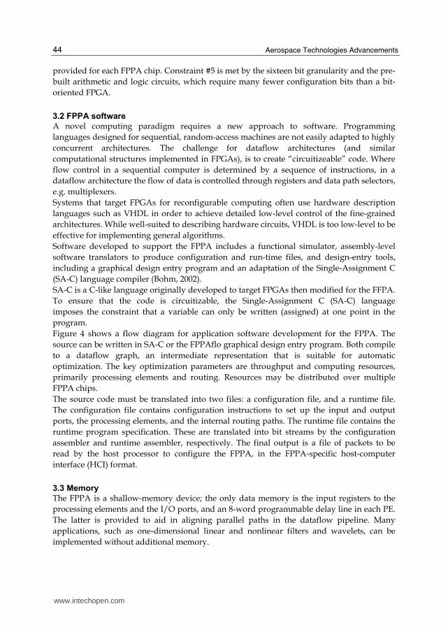
3.2 FPPA software
A novel computing paradigm requires a new approach to software. Programming
languages designed for sequential, random-access machines are not easily adapted to highly
concurrent architectures. The challenge for dataflow architectures (and similar
computational structures implemented in FPGAs), is to create “circuitizeable” code. Where
flow control in a sequential computer is determined by a sequence of instructions, in a
dataflow architecture the flow of data is controlled through registers and data path selectors,
e.g. multiplexers.
Systems that target FPGAs for reconfigurable computing often use hardware description
languages such as VHDL in order to achieve detailed low-level control of the fine-grained
architectures. While well-suited to describing hardware circuits, VHDL is too low-level to be
effective for implementing general algorithms.
Software developed to support the FPPA includes a functional simulator, assembly-level
software translators to produce configuration and run-time files, and design-entry tools,
including a graphical design entry program and an adaptation of the Single-Assignment C
(SA-C) language compiler (Bohm, 2002).
SA-C is a C-like language originally developed to target FPGAs then modified for the FFPA.
To ensure that the code is circuitizable, the Single-Assignment C (SA-C) language
imposes the constraint that a variable can only be written (assigned) at one point in the
program.
Figure 4 shows a flow diagram for application software development for the FPPA. The
source can be written in SA-C or the FPPAflo graphical design entry program. Both compile
to a dataflow graph, an intermediate representation that is suitable for automatic
optimization. The key optimization parameters are throughput and computing resources,
primarily processing elements and routing. Resources may be distributed over multiple
FPPA chips.
The source code must be translated into two files: a configuration file, and a runtime file.
The configuration file contains configuration instructions to set up the input and output
ports, the processing elements, and the internal routing paths. The runtime file contains the
runtime program specification. These are translated into bit streams by the configuration
assembler and runtime assembler, respectively. The final output is a file of packets to be
read by the host processor to configure the FPPA, in the FPPA-specific host-computer
interface (HCI) format.
3.3 Memory
The FPPA is a shallow-memory device; the only data memory is the input registers to the
processing elements and the I/O ports, and an 8-word programmable delay line in each PE.
The latter is provided to aid in aligning parallel paths in the dataflow pipeline. Many
applications, such as one-dimensional linear and nonlinear filters and wavelets, can be
implemented without additional memory.
www.intechopen.com

Reconfigurable Computing for Space
45
Fig. 4. FPPA software design flow
Many applications require larger-scale data memory, however. For example, two-
dimensional image filters typically require “line buffers” to hold past image values.
Sequential processors are typically coupled with random access memory to store
instructions and data, accessible over shared busses. For streaming applications, data
memory is often organized in regular data structures with well-defined access modes: first-
in, first-out (FIFO) queues, last-in, first-out (LIFO) stacks, sequential access, circular buffers,
or two-dimensional matrices representing images or subimages. High-performance FPGAs
are typically equipped with user-definable memory. These large-scale on-chip platforms are
not yet available in radiation-hard form, however.
In the FPPA, program memory is small (128 x 128 bits); each bit controls one module. The
program memory is distributed over the chip into 1x128 bit latch arrays, each co-located
with the module it controls. Data memory is not provided on chip because of the challenges
of implementing large-scale memory in a logic process, and the problem of deciding how
www.intechopen.com

Aerospace Technologies Advancements
46
much memory to incorporate and how to organize it, as this is highly application
dependent.
The FPPA can work with random access memory, but this is very costly in terms of I/O
ports and board-level interconnects, as shared busses are not supported, and dedicated data
busses are required for addresses and data. For this reason, a Reconfigurable Memory
Module (RMM) was conceived to aid in coupling the FPPA with commercial memory chips.
This consists of an interface module configured to generate addresses for a particular
application, interfaced with a commercial memory chip. In one instantiation of the RMM,
the following access modes were implemented:
RMM Data Access Modes 1. Sequential access 2. Last In, First Out (LIFO) stack 3. First In, Last Out (FIFO) buffer 4. Circular (ring) buffer 5. Lookup Table (LUT) 6. Region of Interest (ROI) 7. Histogram The circular buffer defines a beginning and end of a buffer in the memory. Access is
sequential until the end of the buffer is reached; then it wraps around to the beginning.
Lookup table mode (mode 5) is just random access, using one of the data ports for an
address and the other for data. Region of interest mode (mode 6) models the random access
memory as a two-dimensional array (often used to store images), and defines a subarray, or
subimage; sequential accesses sweep horizontally across a row of data elements; when the
end of the row is reached, the address counter moves to the beginning of the next row.
Histogram mode (mode 7) supports histogram calculations, which are sometimes used in
image enhancement and in signal and image analysis. For example, estimating signal
entropy requires calculating
10 2( ) ( )log ( )N
x n nH X p x p x−== ∑ (1)
Where X is a set of N values x0 to xN-1 and p(xn) is the probability of occurrence of value of
element xn. This probability can be estimated by counting occurrences of xn for each n, i.e.,
forming a histogram, then dividing by the total number of samples. This histogram is
initialized by setting each element to zero using sequential access mode. To calculate the
histogram, a data sample is read from a source, and this is used as an index into the
histogram in a read-modify-write operation: the histogram values is read, incremented, then
written back. Finally, the histogram can be read out in sequential access mode. Thus, three
configurations of the RMM are required.
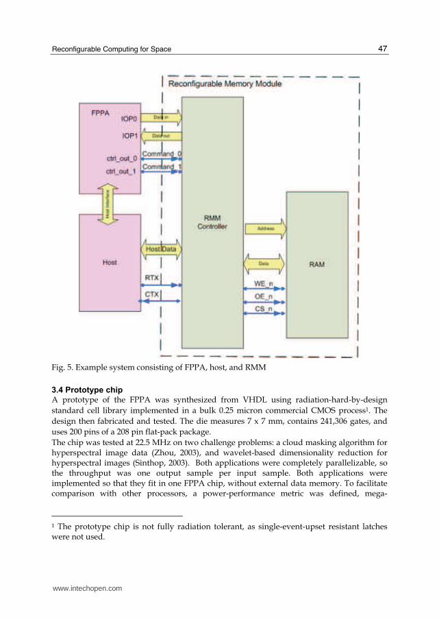
Figure 5 shows a typical arrangement for an FPPA systems consisting of one FPPA, a host
processor, and the RMM. The host configures and initializes both the FPPA and the RMM.
One FPPA data port is used for writing from the FPPA to the RMM, and one for reading
from the RMM into the FPPA. The host communicates with the RMM via an 8-bit data bus
and two asynchronous handshake signals, RTX and CTX. Once the FPPA and RMM are set
up, and the FPPA begins to execute, the host is not longer required. Two control bits,
command_0 and command_1, are sufficient for the FPPA to control the RMM.
www.intechopen.com
Reconfigurable Computing for Space
47
Fig. 5. Example system consisting of FPPA, host, and RMM
3.4 Prototype chip
A prototype of the FPPA was synthesized from VHDL using radiation-hard-by-design
standard cell library implemented in a bulk 0.25 micron commercial CMOS process1. The
design then fabricated and tested. The die measures 7 x 7 mm, contains 241,306 gates, and
uses 200 pins of a 208 pin flat-pack package.
The chip was tested at 22.5 MHz on two challenge problems: a cloud masking algorithm for hyperspectral image data (Zhou, 2003), and wavelet-based dimensionality reduction for hyperspectral images (Sinthop, 2003). Both applications were completely parallelizable, so the throughput was one output sample per input sample. Both applications were implemented so that they fit in one FPPA chip, without external data memory. To facilitate comparison with other processors, a power-performance metric was defined, mega-
1 The prototype chip is not fully radiation tolerant, as single-event-upset resistant latches were not used.
www.intechopen.com

Aerospace Technologies Advancements
48
Fig. 6. Prototype FPPA chip
operations/second-watt (MOPS/watt). Instructions sets vary between processors, so that
one processor may require more machine level instructions to implement a computation
than another. To the system designer, the relevant instructions are those that transform data
as defined in a high-level description of the problem. Here we define an “instruction” as an
arithmetic operator (add, multiply), or a logic operator (shift, AND, etc.).
For the cloud masking algorithm, the FPPA ran at 742 MOPS consuming 0.23 watts, or 3,167
Mops/sec-watt. The FPPA executed the wavelet application with 1080 MOPS consuming
0.48 watts, or 1,849 MOPS/watt.
4. Conclusion
Spacecraft represent one of the application domains that have the most to gain from
reconfigurability, particularly due to the high cost and long delays associated with
designing, building, qualifying and launching a new craft (Lanza 2004). Areas in which
spacecraft can benefit include:
• Tele-alteration: the ability to change configuration and function of a system remotely, increasing mission agility and extending the useful life of the system.
• Resilience and robustness: reconfigurability makes it possible to map out failed components and restore functionality.
• Functionality on demand : when a new function is required, if the configurable resources are in place, remotely configure the required functionality
Adapting commercial technologies to reconfigurable space systems is complicated by the
requirements of small size and weight, low power consumption, and radiation hardness.
This chapter presented an example of a reconfigurable processor developed for space using
radiation-hard-by-design techniques. The goals of the design were to achieve an appropriate
level of functionality to solve a wide range of space computing problems, extensible to
larger-scale problems than can be implemented in one chip, minimal power consumption,
and sufficient radiation hardness for space applications. The architecture implements a
www.intechopen.com

Reconfigurable Computing for Space
49
synchronous dataflow computing model, and is extensible by tiling multiple chips to
increase the size of the dataflow network, and adding reconfigurable memory modules for
applications requiring external data memory.
Reconfigurable computing is becoming a reality, but we can envision extending the concept
of reconfigurability beyond logic to other domains. Software radio is a familiar example, in
which key components of a radio communication system can be altered to adapt to different
frequencies and communication protocols. Reconfigurable analog systems could permit in
situ configuration of sensing and control functions. Reconfigurable pathways (wiring,
optical, fluidic, thermal) could enable software-defined physical systems. A reconfigurable
power infrastructure, and even reconfigurable matter can be conceived to accommodate as-
yet unimagined demands for spacecraft systems.
5. References
Bohm, W.; Hammes, J.; Draper, B; Chawath, M.; Ross, C.; Rinker, R. & Majjar, W. (2002).
Mapping a Single Assignment Programming Language to Reconfigurable Systems,
Supercomputing 21:117-130, 2002.
DeHon, A. (1996). Reconfigurable Architectures for General-Purpose Computing, MIT AI Lab
Report No. 1586, Massachusetts Institute of Technology, Cambridge, MA, USA,
1996.
Donohoe, G; Buehler, D; Hass, K; Walker, W. & Yeh, P.-S. (2007). Field Programmable
Processor Array: Reconfigurable Computing for Space, IEEE Aerospace Conference,
Big Sky, MT, March 3-10, 2007.
Goldstein, S; Schmit,H., Budiu, M., Cadambi, S., Moe,M. & Taylor, R. (2000) “Piperench: a
Reconfigurable Architecture and Compiler”, IEEE Computer, Vol. 33, Issue 4, April
2000, pp. 70-77.
Hauck, S. & Dehon, Andre (2008), Reconfigurable Computing: The Theory and Practice of
FPGA-Based Computation, Elsevier/Morgan Kaufmann, Amsterdam, ISBN 978-0-
12-370552-8.
Holmes, A. & Adams, L. (2002), Handbook of Radiation Effects, Oxford University Press,
Oxford, ISBN-13 978-0198507338.
Lanza, D; Lyke, J.; Zetocha, P; Fronterhouse, D; & Melanson, D. (2004). Responsive Space
through Adaptive Avionics, Space 2004 Conference and Exhibit, American Institute
of Avionics and Aeronautics, AIAA 2004-6116, San Diego, CA, 2004.
Sabde, J; Buehler, D. & Donohoe, G. (2003) Focal Plane Array Sensor Readout Correction on
a Reconfigurable Processor, Proc. 11th NASA Symposium on VLSI Design, Coeur
d’Alene, ID, USA, May 2003.
Sabde, J. (2004). Sensor Data Processing on a Reconfigurable Processor, Master of Science
Thesis, University of Idaho, USA.
Sinthop,K.; Le Moigne, J. & El-Ghazawi, T. (2003). “Automatic Reduction of Hyperspectral
Imagery using Wavelet Spectral Analysis,” IEEE Trans. Geoscience and Remote
Sensing, Vol. 41, No. 4, April 2003.
Tessier, R. & Burleson, W. (2001). Reconfigurable Computing for Digital Signal Processing:
A Survey, Journal of VLSI Signal Processing 28, 7-27, 2001.
www.intechopen.com

Aerospace Technologies Advancements
50
Villasenor, J. & and W. Mangione-Smith, W. (1997). “Configurable Computing”, Scientific
American, June 1997.
Zhou, Y.; P.-S. Yeh,, P.-S.; Wiscombe, W. & S.-C.Tsay, S.-C. (2003) “Cloud context-based
onboard data compression,” Proc. IGARS 2003, Toulouse, July 21-25, 2003.
www.intechopen.com

Aerospace Technologies AdvancementsEdited by Thawar T. Arif
ISBN 978-953-7619-96-1Hard cover, 492 pagesPublisher InTechPublished online 01, January, 2010Published in print edition January, 2010
InTech EuropeUniversity Campus STeP Ri Slavka Krautzeka 83/A 51000 Rijeka, Croatia Phone: +385 (51) 770 447 Fax: +385 (51) 686 166www.intechopen.com
InTech ChinaUnit 405, Office Block, Hotel Equatorial Shanghai No.65, Yan An Road (West), Shanghai, 200040, China
Phone: +86-21-62489820 Fax: +86-21-62489821
Space technology has become increasingly important after the great development and rapid progress ininformation and communication technology as well as the technology of space exploration. This book dealswith the latest and most prominent research in space technology. The first part of the book (first six chapters)deals with the algorithms and software used in information processing, communications and control ofspacecrafts. The second part (chapters 7 to 10) deals with the latest research on the space structures. Thethird part (chapters 11 to 14) deals with some of the latest applications in space. The fourth part (chapters 15and 16) deals with small satellite technologies. The fifth part (chapters 17 to 20) deals with some of the latestapplications in the field of aircrafts. The sixth part (chapters 21 to 25) outlines some recent research efforts indifferent subjects.
How to referenceIn order to correctly reference this scholarly work, feel free to copy and paste the following:
Donohoe, Gregory W. and Lyke, James C. (2010). Reconfigurable Computing for Space, AerospaceTechnologies Advancements, Thawar T. Arif (Ed.), ISBN: 978-953-7619-96-1, InTech, Available from:http://www.intechopen.com/books/aerospace-technologies-advancements/reconfigurable-computing-for-space