Switches and indirect networks Computer Architecture AMANO, Hideharu Textbook pp. 92~13 0.
Upload
jeffry-edwin-hornCategory
view
223download
2
Reconfigurable Architectures
AMANO, Hideharu
hunga @ am . ics . keio . ac . jp

Reconfigurable System( Custom Computing Machine ) A target algorithm is executed directly with
a hardware on SRAM-style FPGA/PLDs. High performance of special purpose machine
s. High degree of flexibility of general purpose ma
chines. A completely different execution mechanis
m from a stored program computers.

PLD(Programmable Logic Device)
Integrated Circuit whose logic function can be defined by users.
Standard IC,ASIC ( Application Specific IC)
SPLD( Simple PLD) / PLA( Programmable Logic Array) Small scale IC with AND-OR array
CPLD (Complex PLD) Middle scale IC with AND-OR array
FPGA(Field Progarmmable Gate Array) Large scale IC with LUT
Caution! Terms are not well defined!

1990 20001980
10K
100K
1M
10M
Gate number
Increasing PerformanceFrom 1991-2000Amount of gate: X45Speed: X12Cost:1/100
Fuse-PLA
EEPROM-SPLD
SRAM-FPGA
CPLD
Anti-fuseFPGA
Hierarchical structureEmbedded CoreLow voltage
Rapidly development of PLD

SPLD ( Simple PLD:AND-OR/Product-term )
NOT ANDOR
Arbitrary logic is realized bychanging the AND-OR connection

NOT ANDOR
A B C D
A & B
AND/OR connection example
C & D
A&B | C&D

LUT : Look Up Table
Look Up TableROM/RAM…
Address…
Data
A simple ROM/RAM can used as arandom logic.
ABC000001010011100101110111
Z00010001
Z00010001
CB
A
A combination of memory andmultiplexers are commonly used.

An example using LUT : Look Up Table
ABC000001010011100101110111
Z00010001
Z00010001
CB
A
1 1 0
1

Device for flexibility (1)
Anti-fuse type Program by destruction of isolation with high v
oltage High speed but One-time ACTEL 、 Quicklogic
EEPROM ・ Flash-ROM Switches for connections are realized by floati
ng gates. Re-programmable Lattice 、 Altera’s MAX series

Device for flexibility (2) SRAM
Data on SRAM represents look up table and wire connection. ISP (In System Programming) is available. The configuration data is erased, when the power turns off. Suitable for a large scale FPGA. Recently, rapidly advanced. Xilinx XC 、 Altera FLEX, Lucent ORCA The advanced series: Xilinx Virtex, Altera APEX
その他 Magnetic memory DRAM

AND-OR array vs. LUT
AND-OR array ( product-term ) Efficient for logic with multiple outputs There is a type of logic which cannot be realized. Suitable for EEPROM and Flash-ROM
LUT Any logic can be realized. Efficient for logic with a single output Suitable for Flash-ROM, Anti-fuse, and SRAM.
Sequential circuits
AND ・ ORarray
or
LUT
D Q
D Q
D Q
D Q
Input Output
FeedBack
Sequential circuit (state machine) can be builtby attaching Flip-flops and feed back loops.
DQ
Q
Feed back
From AND/OR array
OutputModule

CPLD (Complex PLD)
SPLD
ProgrammableSwitch
SPLD
SPLD SPLD
SPLD
SPLD
Altera’s MAX
Matrix of SPLDs Programmable Switch
SPLD
2-dimensional Array

FPGA(Field Programmable Gate Array)LUT
F.F
Configurable LogicBlock
SwitchBlock
Connection Block
IOB
island style
LUT and interconnectionis decided withconfiguration data

Architectures and devices
SPLD
CPLD
FPGA
Anti-fuse
EEPROM
Flash-ROM
SRAM
High speed middle sizeOne-timeACTEL , Quicklogic
Large scaleRapidly developmentXilinx 、 Altera
High speed small/middle sizeRe-programmableDelay is predictableLattice , Altera , Xlinx

Recent PLDs High-end: a large scale chip with hierarchical structu
re : Xilinx’s Virtex II、 Virtex-4/LX, Altera’s Stratix-3
System on Programmable Device Providing DLL , CPU 、 DSP, ROM, RAM, Multiplier, High
speed link, and other hard IPs. Xilix’s Virtex-4/EX,FX, Altera’s Stratix-3
Specialized for mass-production Low cost : Xilinx’s Spartan, Altera’s Cyclone
Low voltage, Multiple voltages, and Low power consumption

Process Products Name LUT Power350nm XC4000 XC4085KLA 7448 3.3V
250nm XC4000 XC40250KV 20102 2.5V
220nm Virtex XCV1000 27648 2.5V
180nm Virtex-E XCV2000E 43200 1.8V
150nm Virtex-II XC2V800O 104882 1.5V
130nm Virtex-II Pro
XC2VP125 125136 1.5V
90nm Virtex-4 XC4VLX200 200488 1.2V
65nm Virtex-5 XC5VLX330 51840slice 1.0V
40nm Virtex-6 XC6VLX760 118560slice 1.0V
28nm Virtex-7 XC7VX1140T 1139200slice 0.9V
Process and parameters ( Xilinx co. )

Xilinx Virtex II
Programmable IOs
Configurable Logic
DCM IOB
RAM Multiplier
GlobalClockMUX
LUT Carry DQ
LUT Carry DQ
Slice
Slice X 2 → CLB (Configurable Logic Block)
100000 CLBs3Mbit

Altera Stratix II
Mega RAMBlocks
M4K RAMBlocks
M512 RAMBlocks
PLL
DSP Blocks
LAB : Logic Array Blockconsisting of 10 LE (4-input LUT and F.F.)
Hierarchical Interconnect

SoPD (System on Programmable Device)DCM
Rocket I/O, Multi-Gigabit Transceiver
Power-PC
MultiplierBlock RAM
CLBs
Various kinds of cores areembedded on an FPGA
XilinxVirtex-II Pro

FPGA vs. ASIC[Kuon:FPGA2006] Pure FPGA without hard macros
Area :40 X Speed :1 /3.2X Power: 12X
FPGA with hard macros Area: 21X Speed: 1/2.1X Power: 9X

Spartan-3 Power Consumption [tuan2006]
ClockLogicRouting
LogicRoutingConfig SRAM
Dynamic Powerabout 200mW (3S1000)
Static Powerabout 60mW(3S1000)

90nm 65nm 45nm 40nm
Virtex-4LX/FX/SX200000LC
Stratix-IV/E/GX/GT 531200LE
Stratix-III/L/E 338000LE
Stratix-II/GX 179400LE
Cyclone IV/E/GX 149760LE
60nm
Cyclone III/LS 119088LE
Cyclone II 68416LE
Virtex-6LXT/SXT/ HXT/CXT760000LC
Spartan-6LX/LXT150000LC
Virtex-5LX/LXT/SXT/ FXT/TXT330000LC
ExtentedSpartan-3A N/DSP53000LC
High-end
Low-cost
Recent technologies and products
X1.5-X2.5/ generation
High-end/Low-cost: X3- X5

Slice structure of Virtex-6LUT6inX15inX2
CarryFF
FFMUX
6bit MUX
LUT6inX15inX2
CarryFF
FFMUX
6bit MUX
LUT6inX15inX2
CarryFF
FFMUX
6bit MUX
LUT6inX15inX2
CarryFF
FFMUX
6bit MUX
Virtex-6 manual

SliceX0Y0
SliceX1Y0
CLB
COUT COUT
SliceX2Y0
SliceX3Y0
CLB
COUT COUT
SliceX2Y1
SliceX3Y1
CLB
COUT COUT
SliceX1Y0
SliceX1Y1
CLB
COUT COUT
CIN CIN CIN CIN
Virtex-6 CLBs
Virtex-6 manual

LUT6in
FFMUX
4bitdata MUX
LUT6in
adder1FF
MUX4bitdata MUX
adder2
shared_arithcarry
reg_carry
4-in LUT X 25-in LUT + 3-in LUT5-in LUT + 4-in LUT 1-input shared5-in LUT + 5-in LUT 2-input shared6-in LUT6-in LUT + 6-in LUT 4-input shared
Stratix-IV ALM Structure
Stratix-IV manual

LABLocalInterconnect
MLABLocalInterconnect
ALMs
Stratix-IV LAB structure
Stratix-IV マニュアルより

Power Gating for Spartan-3
ConfigSRAMs
ConfigSRAMs
InterconnectSwitch Matrix
CLB
ConfigSRAMs
PowerGate
Virtualground
FPGA Core
Tile
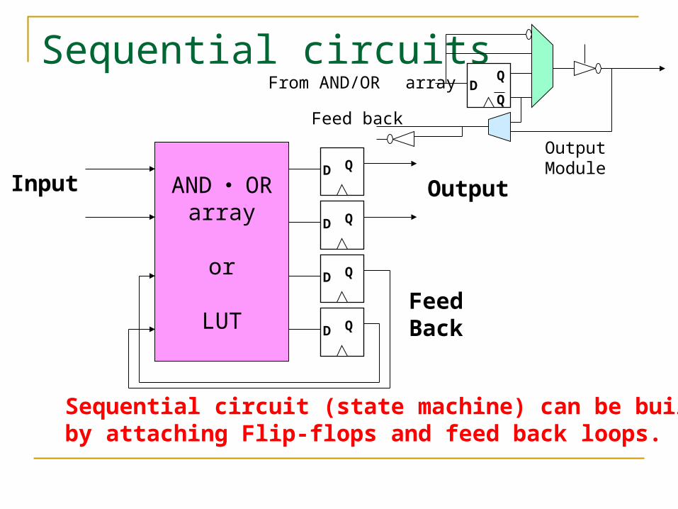
Low-power FPGAs
Actel: ProASIC 3/E→ IGLOO Flush ROM IGLOO: with ARM core Flash freeze: Low power stand-by mode(2μW)
Silicon Blue ICE65 series Embedded Flash memory (NVCM) 5mA(1792cells,32MHz) 9mA(3520cells,32MHz)
Altera Arria 、 Arria-II Low Power Mid-range 8-input LUT

QuickLogic
Lattice GAL

Altera FLEX10K

Qucklogic
Xilinx Vertex

Design of PLDs Mostly designed with common HDL ( Verilog-HDL,
VHDL) C level entry is used recently: Handel-C(Ceroxca)
Synthesis, optimization, place and route is automatically done by vendors’ tools. Integration and combination of tools from various venders a
re used recently. For large circuit, a long time is required especially for place
and route. Using IPs, clock/DLL adjustment is manually done. Optimization techniques are different from vendors/product
s.

Reconfigurable System( Custom Computing Machine ) A target algorithm is executed directly with
a hardware on SRAM-style FPGA/PLDs. High performance of special purpose machine
s. High degree of flexibility of general purpose ma
chines. A completely different execution mechanis
m from a stored program computers.

Flexibility
Performance
CPU
for i=0; i<K; i++X[i]=X[i+j]
.....
CPUSoftware
ASIC
DesignA
DesignC
DesignD
DesignB
FPGAs
High Performance and Flexibility
Refonfigurable Systems

How enhance the performance ? Performance enhancement by hardware
execution itself The overhead of software execution (Instruction
fetch, data load to registers, and etc.) The overhead of using fixed size data. The overhead of using only two way branches.
The key of performance improvement is parallel processing
However, these benefits are not so large, for embedded CPU and DSPare highly optimized.

Parallel processing in reconfigurable systems Various techniques can be used
SIMD execution Pipelined structure Systolic algorithm Data driven control
Parallel execution other than calculation Parallel data access using internal memory units Parallel data transfer including I/O accesses

SIMD (Single Instruction-stream/Multiple Data-stream)-like calculation
Stream Data in Stream Data out
InternalMemory module
Processing part
The same instruction is applied to different data streamIn Reconfigurable Systems, the operation is not required to be same( SIMD-like calculation )

Pipelined structure
Stream Data 1Stream Data 1
InternalMemory module
Processing part
The stream is divided and inserted periodically.
Stream Data 2Stream Data 3Stream Data 4Stream Data 5Stream Data 2
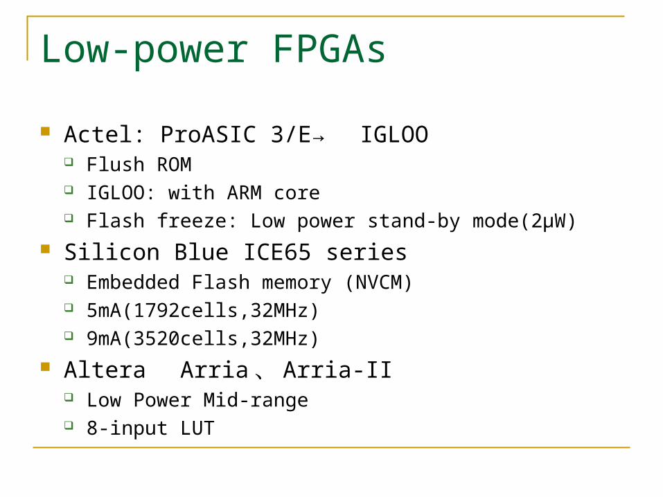
Systolic Algorithm
Data x
Data y
Computational array
Data stream x , y are inserted with a certain interval.When two stream meet each other, a calculation is executed.→ Systolic: The beat of heart

Band matrix multiply y=Ax
a
x
a11 a12 0 0
a21 a22 a23 0
0 a32 a33 a34
0 0 a43 a44
X+
yiyo
yo= a x + y i
y0
y1
y2
y3
x0
x1
x2
x3
=

Band matrix multiply y=Ax
X +
a11
x1
a12 a21
a22
a23 a32
a11 a12 0 0
a21 a22 a23 0
0 a32 a33 a34
0 0 a43 a44
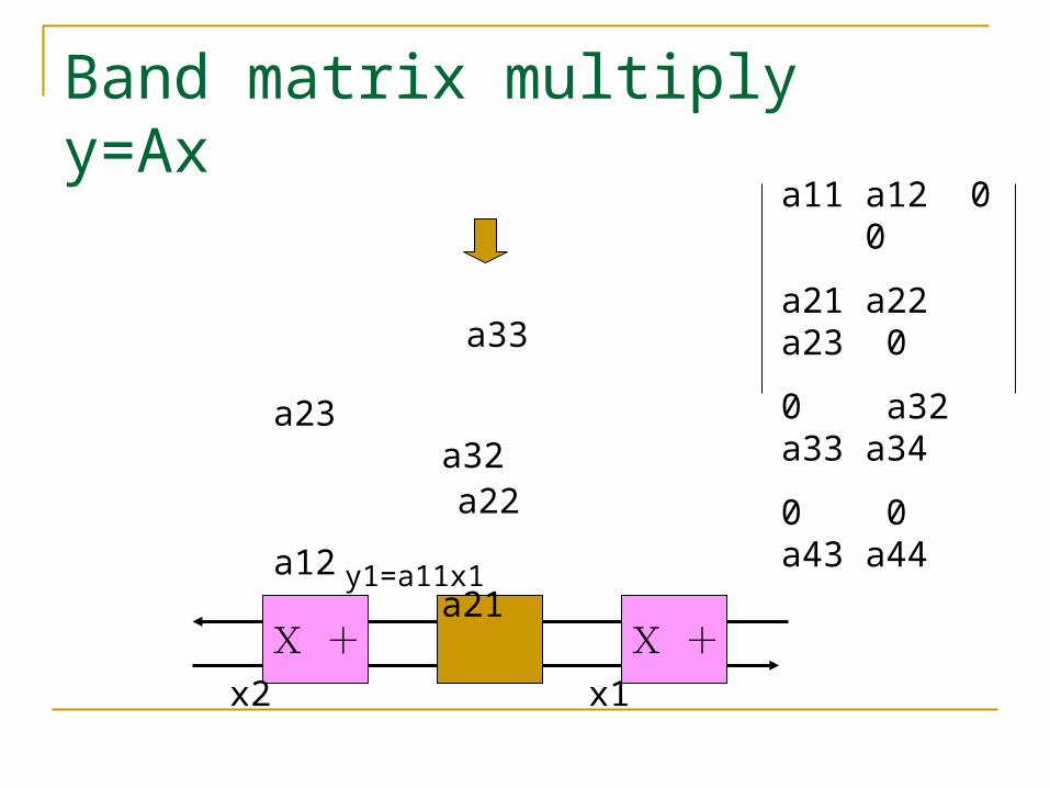
Band matrix multiply y=Ax
X +X +x1
a12 a21
a22
a23 a32
a11 a12 0 0
a21 a22 a23 0
0 a32 a33 a34
0 0 a43 a44
a33
y1=a11x1
x2

Band matrix multiply y=Ax
X +x1
a34 a43
a22
a23 a32
a11 a12 0 0
a21 a22 a23 0
0 a32 a33 a34
0 0 a43 a44a33
y2=a21 x1
x2x3
y1=a11 x1+ a12 x2

Band matrix multiply y=Ax
X +X +
a34 a43
a44
a23 a32
a11 a12 0 0
a21 a22 a23 0
0 a32 a33 a34
0 0 a43 a44
a33
y2=a21 x1+ a22 x2
x2x3

Band matrix multiply y=Ax
X +
a34 a43
a44
a11 a12 0 0
a21 a22 a23 0
0 a32 a33 a34
0 0 a43 a44
a33y2=a21 x1+ a22 x2+ a23 x3
x2x3
y3= a32 x2

Data flow algorithm
x
+
x
+
a bc
d e
(a+b)x(c+(dxe))
The process is activatedwith the available of tokens(data)
The overhead of synchronization is large.

Data flow analysis and hardware generation
Data Flow Language
ConfigurationData
Data Flow Graph
Graph Decomposition
HDLDescription
Suitable for automatic generation of hardware

Applications No flexible program change No IEEE standard floating point Not memory bounded
Image processing, analysis, pattern matching, Logic simulation, Fault simulation. Neural network simulation. Encryption /Decryption Queuing Model 、 Markov Analysis Electric Power Flow Censer processing
Efficient use of on the fly processing. Communication control 、 Protocol control Software radio

Large Scale Reconfigurable Systems
…μP μP … …RU RU ……μP μP …RU RU
Interconnection/Shared memory
…μP RU …μP RU …μP RU …μP RU
Interconnection/Shared memory
Hetero nodes using homo cores : SRC6, SGI RASC
Homo node using hetero cores : Cray XD-1, XT4(XR-1)
μP
Stand-alone : SPLASH, RASH,BEE2
…RU RU …RU RU …RU RU
Interconnection/Shared memory
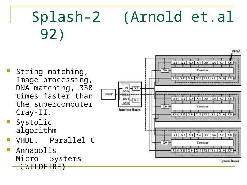
Splash-2 (Arnold et.al 92)
String matching, Image processing, DNA matching, 330 times faster than the supercomputer Cray-II.
Systolic algorithm VHDL, Parallel C Annapolis Micro
Systems ( WILDFIRE)

RM-IV (Kobe Univ.)
FPGAmem .
FPGAmem . FPGAmem .
FPGAmem .
FPGAmem .
FPGAmem . FPGAmem .
FPGAmem .
FPGA mem .
FPGA mem .FPGA mem .
FPGA mem .
FPGA mem .
FPGA mem .FPGA mem .
FPGA mem .
FPIC
Interface

RASH ( Mitsubishi )
FPGA Altera FLEX10K100A (62K-158KGate)
→ Changed into Stratix, then changed into Virtex II
EXE-board controller
FPGA FPGA FPGA FPGA
FPGA FPGA FPGA FPGA
PCI Local-bus
PCI-bus
PCI-bus I/F
Clocks / Cont. signals
SRAM( 2MB )
Local-bus
Mesh + Bus
2 clock lines
PCI bus I/F
A large SRAM
DRAM daughter board
6 boards consist one system unit.
Shared Memory with multiple FPGAs

ATTRACTOR ( NTT )
RISC
FPGA
RISC
FPGA
RISC
ATMI/O
RISC
ATMSW
RISC
Buffer
RISC
RAM( LUT)
MPU
Mem.
Compact PCI
Ethernet
High speed serial link ( 1Gbps )
Special purpose system for ATM cut-through router
Combination with various units

CRAY-XD1 : • AMD Opteron• 1board is consisting of 2CPUs + FPGA ( Virtex II Pro) • 1 rack provides 6 boards• A high speed network called Rapid Array is used• Interconnection between FPGAs can be done with Rocket I/O

SGI RASC•Accelerator for SGI’s NUMA Altix •Virtex II XC2V6000 and another Virtex for control•Directly connected into the controller with NUMAlink4

ReCSiP ( Keio Univ. )
Virtex-II
64MB SDRAM
4MB SSRAM
QuickPCI
Local ClockGenerator
ConfigrationControl
64bit Local Bus
64bit/66MHz PCI Bus
via USB via PCI
Configuration
XC2V6000
Accelerator for bioinformaticsPowerful simultaneous access facility of external RAMs

ReCSiP Board
ReCSiP-2QDR-SRAM (4MB x 4)
Virtex-II Pro (XC2VP70)PCI-IF
(QL5064)
DDR-SDRAMSO-DIMM

ReCSiP
Automatic generation of solvers
Solver Library
SBML description
Optimizer
CAD Tools
SchedulerSolver Set
FPGA Board
HDL for Solvers is generated
Control between solvers

Dynamically Reconfigurable Processors Coarse grain structure Parallel processing →Reconfigurable Processor
Array Dedicated for stream processing
Distributed memory High speed dynamic reconfiguration
Multicontext Multicast/Broadcast of configuration data inside the chip On-line Configuration
C-base design
Short history of Dynamically Reconfigurable
Processors 1990 1995 2000 2005
FPGA with DynamicReconfiguration
Processor withReconfigurableInstructions
MPLD(Fujitsu)
WASMII(Keio)
Time MultiplexedFPGA(Xilinx)
DRL(NEC)
GARP(UCB)CHIMAERA(NorthWestern Univ.)
Xpp(PACT)CS2112(Chameleon)
DRP(NEC elec.)
DAPDNA/2(IPFlex)DFabric(Elixcent)
Kilocore(Rapport)PipeRench(CMU)
X-bridge(NEC ele.)
DAPDNA/IMX(IPFlex)
S-5(Stretch) S-6(Stretch)
FE-GA(Hitachi)
The 1st Generation The 2nd Generation
A lot of commercialsystems
DISC(Brigham Young Univ.)

Product Vendor Context Data PE
D-Fabric Panasonic Deliver 4 Homo
Xpp PACT Deliver 24 Homo
S5/S6 engine Stretch Deliver 4/8 Hetero
CS2112 Chameleon Multi-C (8) 16/32 Homo
DAPDNA-2 IPFlex Multi-C (4) 32 Hetero
DRP-1 NEC electronics Multi-C (16)
8 Homo
X-bridge NEC electronics Multi-C(32) 8 Homo
Kilocore Rapport Multi-C 8 Homo
ADRES IMEC Multi-C (32)
16 Homo
FE-GA Hitachi Multi-C 16 Hetero
For Car-tuners SANYO Multi-C(4) 24 Homo
Cluster Fujitsu Multi-C 16 Hetero
Dynamically Reconfigurable processors

Coarse Grain Structure of PE
Instruction
Rou
tin
gM
UX
Rou
tin
gM
UX
Register&
Mask
Register&
Mask
OP Register
RegisterBarrelShifter
Chameleon CS2112Kress Array II

PAC PACI/O
I/O
PACI/O
I/O
I/O
I/O
PACI/O
I/O
SCM
CM
CM CM
CM
Configuration controller
PAC: Processing Array Cluster)CM: Configuration ManagerSCM: Supervising CM
Xpp (PACT Informations technologie)
PAE
Xpp64 (8x8 PAC) is available.Configuation requires 100s’ clocks.PAE adopts 24bit-width, Clock cycles is 40MHz .

Panasonic(Elixent ) DFA1000
ALU R
RR
ALU R
RR
ALU R
RR
ALU R
RR
ALU R
RR
ALU R
RR
ALU R
RR
ALU R
RR
4 bit ALU Register RAM basedswitch box

Multicontext structure
Mul
tipl
exer
SRAM slots
n
Logic cells
1
2
Input data
Output data
Logic cellsLogic cellsContext
A PE provides multiple configuration RAM sets
One clock context switching can be done.
Context pointer
PEs or Switches
Contextmemory

Chameleon CS2112
ReconfigurableProcessing
Fabric
128-bit RoadRunner Bus
PCI Cont. RISC CoreMemory
Controller
DMASubsystem
ConfigurationSubsystem
160-pin Programmable I/O
32-bit PCI Bus 64-bit Memory Bus

Reconfigurable Processing Fabric in Chameleon
DPU
CTLLM
Tile 0
Slice 0
DPU
CTLLM
Tile 0
Slice 3
108 DPU(Data Path Unit)s consists 4 Slices ( 3Tiles each )
1Tile: 9DPU = 32bit ALU X 7 16bit + 16bit multiplier X 2
8 instructions stored in the CTL are executed in the DPU.
The CTL can select the next instruction in the same cycle.
Configuration can be changed by loading a bit stream.

Ipflex DAP/DNA-2
DAP(RISC)
DMAController
InterruptController
TimerSROM IF
GPIOUART
Serial IF
DD
R S
DR
IF(64b
it 166MH
z)P
CI IF
(32bit 66M
Hz)
DNA loadbuffer
DNA direct I/O(Async. In)
DNA storebuffer
DNA direct I/O(Async. out)
DNAMatrix
BS
U
368 PEsALU,Memory,Delay etc.Heterogeneous

An example PE structure
FF FF
Shift/Mask Shift/Mask
FFFF
ALU
ALU
FF
FF FF
Shift/Mask Shift/Mask
FFFF
ALU
FF

Tile
DRP (Dynamically Reconfigurable Processor: NEC)
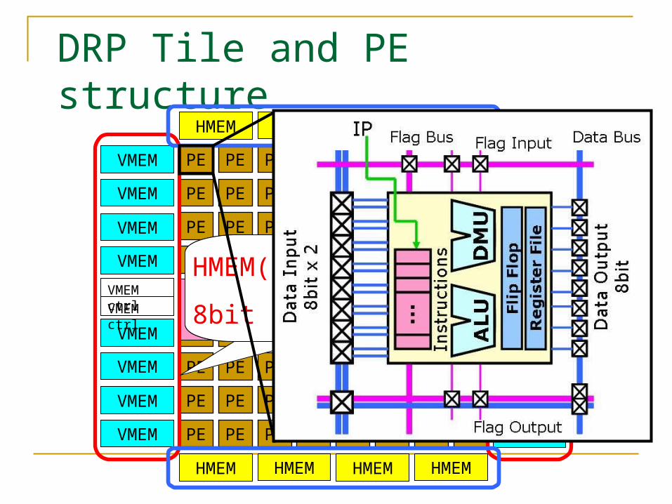
DRP Tile and PE structure
PE
PE
PE
PE
PE
PE
PE
PE
PE
PE
PE
PE
PE
PE
PE
PE
PE
PE
PE
PE
PE
PE
PE
PE
PE
PE
PE
PE
PE
PE
PE
PE
PE
PE
PE
PE
PE
PE
PE
PE
PE
PE
PE
PE
PE
PE
PE
PE
PE
PE
PE
PE
PE
PE
PE
PE
PE
PE
PE
PE
PE
PE
PE
PE
HMEM HMEM HMEM HMEM
HMEM HMEM HMEM HMEM
VMEM
VMEM
VMEM
VMEM
VMEM
VMEM
VMEM
VMEM
VMEM
VMEM
VMEM
VMEM
VMEM
VMEM
VMEM
VMEM
State Transition Controller
VMEM ctrlVMEM ctrl
VMEM ctrlVMEM ctrl
VMEM(2-port memory)
8bit × 256entry
HMEM(1-port memory)
8bit × 8092entry

Context control for DRP0
1
2
3
4
5
Data input
Data output
1. Context switching
2. Parallel processing in a context3. Serial execution in a context
Description in BDLDRP compiler controls 3-dimensional assignment

Main Advantage: Low power consumptionWhy low power ?1. No redundant hardware
There are no instruction fetch mechanisms, cache, TLB, and etc.→ Of course, it cannot be a general purpose engine, but enough f
or an accelerator. A bare datapath works only for computation.
2. Parallel Execution with a number of PE s Much lower clock frequency can be used to achieve the same pe
rformance as other architectures. The main problem is leakage power, but can be suppressed by p
ower gating techniques.10X energy efficient compared with DSPs.5-50X with FPGAs.Sometimes similar to that for hardwired logic.

The main limitations as an accelerator in SoCs The data must be stored in the memory modules
placed around the PE array. If the data is more than the memory, it is hard to be treated.
If the required contexts are more than its context memory, the operational speed is much degraded. The virtual hardware mechanism is provided but there is a
certain limitation. The performance is not so improved for problems
without parallelism.
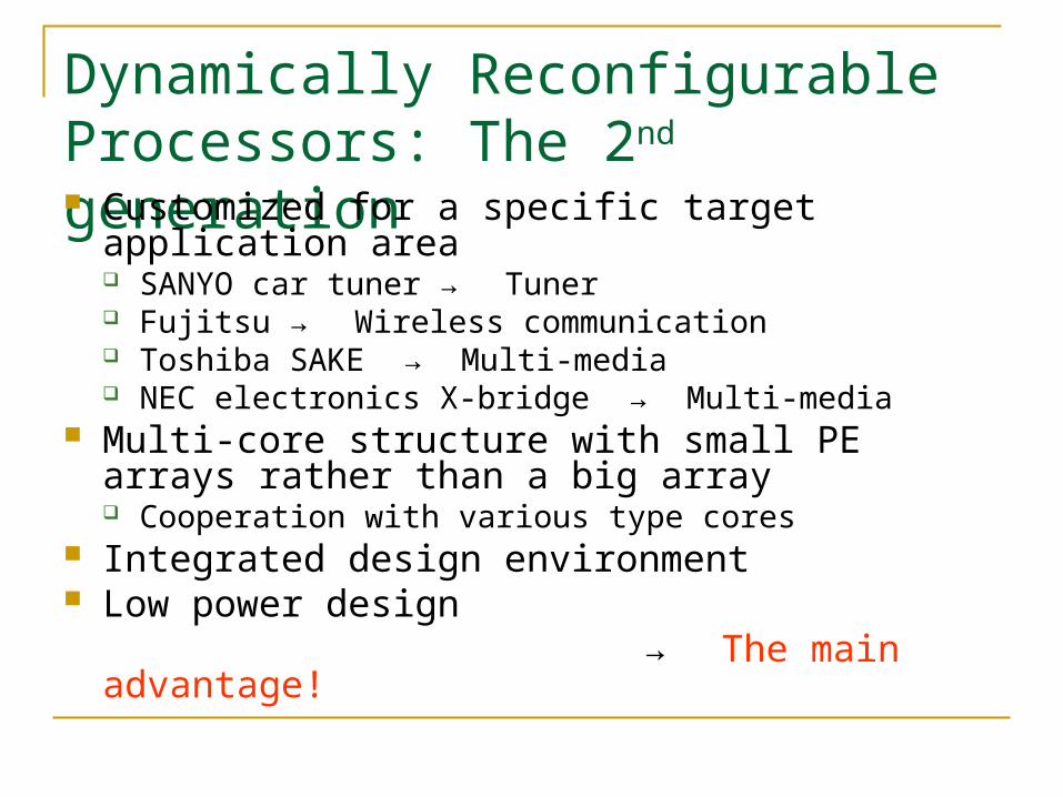
Dynamically Reconfigurable Processors: The 2nd generation Customized for a specific target application area
SANYO car tuner → Tuner Fujitsu → Wireless communication Toshiba SAKE → Multi-media NEC electronics X-bridge → Multi-media
Multi-core structure with small PE arrays rather than a big array Cooperation with various type cores
Integrated design environment Low power design → The main advantage!

X-bridge: NEC electronics (2008)
CPUMIPS
JTAG
I-CD-C
UA
RT
UA
RT
CS
IG
PIO
INTC
GeneralPort8bX4
DMA
SPL
DMA
WorkRAM(1kB)
PCIexpHB/EP(1-lane)
PeriphI/F
10/100EtherMAC
DMA
PCIHost/
Target
DDR2SDRAM
CTR
DMAPCIexpHB/EP(1-lane)
STPEngine
64bit on chip bus (266MHz)
64bi
t M
emor
yS
witc
h (2
66M
Hz)SPL
SPLSPL
SPLSPL
SPLSPL SPL
Nconnect
DynamicallyReconfigurableCore512PE(8bit)32-context
Providing the virtual hardware
mechanism
DMA controller hides the communication
overhead
From Invited talk in Design Gaia.2008

Mixture of SIMD and DRP units:Toshiba’s SAKE
Host Processor
I/O Buffer (Data RAM)
Formatter0Write
Control
Host I/F
System Memory
Inter-Unit Buffer (Data Registers)
Dynamically Reconfigurable Units(Indenepndently Controlled)
Code Buffer (Code RAM)
Formatter1AUX0AUX1
Optimized forStream Processing
SIMD Units
codedata
Our Architecture
From FPT2007 Tutorial session

The Architecture (Formatter)
data A
Cfg
Me
m
data B
Shuffle
16-bit ALU x 8PE
Xbar In
validID
PE
PE w/o Shuffle
Xbar In
Xbar Out
Cfg Controller
CodeMem
Simple Hardware•Pipeline registers only•No intra-PE data transfer•PE:4 cfgs, Xbar: 16cfgs•ALU, shift & absolute ops only
PE
PE
Xbar In: Formatter0 onlyXBar Out: Formatter1 only
128 128
Suitable for batterfly operations
19
64
From FPT2007 Tutorial session

SANYO’s Car tuner DRP
ALU ALU ALU ALU ALU ALU
ALU ALU ALU ALU ALU ALU
ALU ALU ALU ALU ALU ALU
ALU ALU ALU ALU ALU ALU
main memory
Out
In
sequencer
command memory
Feedback
ALU array

ALU ALU ALU ALU ALU ALU
ALU ALU ALU ALU ALU ALU
ALU ALU ALU ALU ALU ALU
ALU ALU ALU ALU ALU ALU
L 1
L 2
L 3
L 4
L 1L 2L 3L 4
Th1-1Th1-2
Th1-3Th1-4
Th2-1Th2-2
Th2-3Th2-4
Th3-1Th3-2
Th3-3Th3-4
Th4-1Th4-2
Th4-3Th4-4
Th1-5Th1-6
Th1-7Th1-8
Th2-5Th2-6
Th2-7
Pipelined execution of 4 threads

Fine carrier frequency offset estimation/correctionCluster0
I
QI
Qto FFT
Cluster4 Cluster5 Cluster6
Cluster1
Cluster2
DIV ATAN
Reg incluster0
Cluster0
Cluster3data outcontrol
I
Qto FFT
I
Q
LT1
LT2
self-correlation
phase offset calculation
Cluster1Cluster6(through)
Cluster0Reg
correction offset calculation in phase
polarCluster2complexmultiply
I
Q
Cluster3data outcontrol &
clip
I
Q
a) Fine carrier frequency offset estimation for LT1
b) Fine carrier frequency offset estimation for LT2
c) Fine carrier frequency offset correction for SIGNAL and DATA

ALU
ALU
ALU
ALU
ALU
ALU
ALU
ALU
MLT ALU
ALU
ALU
ALU
ALU
ALU
ALU
ALU
ALU
ALU
ALU
ALU
ALU
ALU
ALU
ALU
MLT
MLT
MLT
MLT
MLT
MLT
MLT
Crossbar Network
LS
LS
LS
LS
LS
LS
LS
LS
LS
LS
MEM
MEM
MEM
MEM
MEM
MEM
MEM
MEM
MEM
MEM
Configuration Manager
Sequence Manager
BusInterface
Computational Cell Array
Interrupt/DMA request
I/Oport
Load/StoreCells
LocalMemory
Hitachi’s FE-GA

Heterogeneous Multi-Core using FE-GA
SH-4
LPM
FVR
LDM
DSM
DTU
Network Interface
CPU0
FE-GA
LPM
FVR
LDM
DSM
DTU
Network Interface
DRP0CPU1 DRP1
CPU2 CPU3 DRP2 DRP3
On-Chip CSM
Network Interface
The codes are generated by a
parallelizing compiler and
standard APIs.

Examples
High speed configuration PACT xpp Elixent DFA NTT PCA
Multicontext Chameleon CS2112 IPFlex DAP/DNA NEC DRP CMU PipeRench SONY Virtual Mobile Engine (Embedded in PSP)
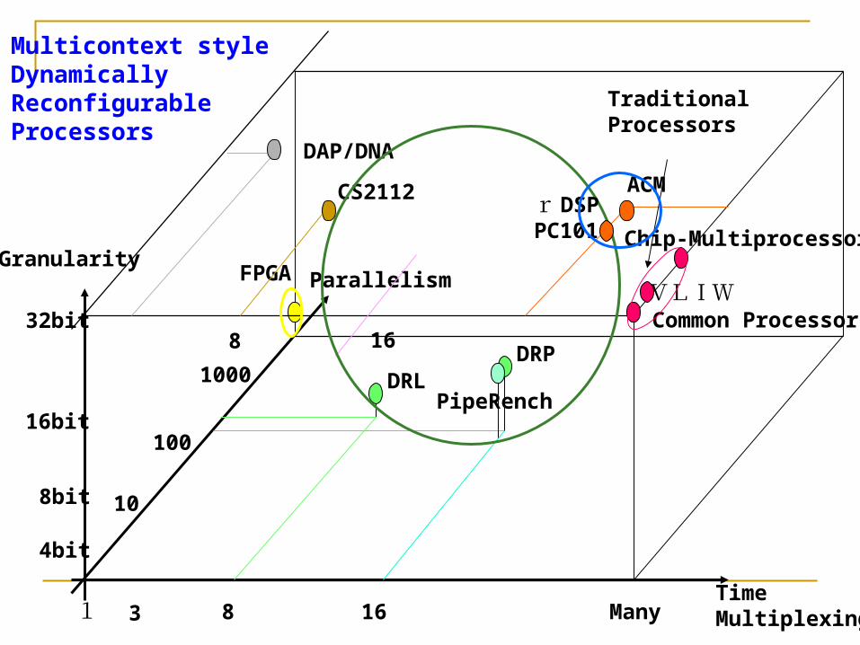
1 3 8 16 ManyTimeMultiplexing
ParallelismGranularity
10
100
1000
32bit
16bit
8bit
4bit
FPGA
Common ProcessorVLIW
Chip-Multiprocessor
ACM
DAP/DNA
DRP
PipeRenchDRL
Multicontext styleDynamically ReconfigurableProcessors
8 16
CS2112
TraditionalProcessors
r DSPPC101

Dynamically Reconfigurable Processors Coarse grain architecture, somehow like on-chip multiprocessors,
while somehow like FPGA. Rapidly development from 2001 They don’t find killer application ( Chameleon’s fail ) High level language development environment has not been well
established. A lot of competitors
High performance embedded processors Chip multiprocessors Application Specific Configurable Processors DSP Standard FPGA/CPLD System On Chip

Open Problems What’s difference between a Program and Configuration Data
Reconfigurable Processor Array = a VLIW machine with an extremely large instructions (Configuration data)
How frequent should Configuration change? Every-clock-context switching is not advantageous from the
viewpoint of consuming power. However, if configuration is rarely switched, dynamic
reconfiguration function is useless. How is grain size of Processing Element decided ?
8-32bit calculators are correct solution? Is it a only escape way from Xilinx’s patent ?
How is the balance between calculators and controllers ? Since DRP focuses on calculators, it is difficult to implement
complicated control. Does the node balance of ACM correct ?

Summary
Another computing system than stored program computers.
Not a perfect replace of stored program type computers.
Advance of the semiconductor techniques directly enhance the performance.
A lot of problems and subjects to research.

Historical flow of computer systems
ENIAC
EDVAC 、 EDSAC
IBM machines
RISC, Intel’s microprocessorsReconfigurableMachine

Exercise
There is a systolic array which multiplies 8 x 8 tri-diagonal matrix A with a size 8 vector x. Compute the number of clock cycles for the multiply. Here, the time when the first element of x reaches to the left-most array is assumed to be time 0.