Recent Developments in High Resolu- tion Delta-Sigma ...
10
Journal of Semiconductor Engineering Vol. 2, Issue 1, March 2021 https://doi.org/10.22895/jse.2020.0104 Received 1 December 2020, Revised 29 December 2020, Accepted 18 January 2021 ISSN(On-line) 2733-6719 1 Recent Developments in High Resolu- tion Delta-Sigma Converters Jaedo Kim, and Jeongjin Roh Department of Electrical Engineering, Hanyang University, Ansan 15588, Korea Corresponding Author: Jeongjin Roh ([email protected]) Funding Information: This work was supported by the National Research Foundation of Korea (NRF) grant funded by the Korea government (MSIT) (No.2019R1A2C2085189). This research was also supported by the MSIT (Ministry of Science and ICT), Korea, under the ITRC (Information Technology Research Center) support program (IITP-2020-2018- 0-01421) supervised by the IITP (Institute of Information & communications Technology Planning & Evaluation). ABSTRACT This review paper describes the overall operating principle of a discrete-time delta-sigma modu- lator (DTDSM) and a continuous-time delta-sigma modulator (CTDSM) using a switched-capac- itor (SC). In addition, research that has solved the problems related to each delta-sigma modulator (DSM) is introduced, and the latest developments are explained. This paper describes the chopper- stabilization technique that mitigates flicker noise, which is crucial for the DSM. In the case of DTDSM, this paper addresses the problems that arise when using SC circuits and explains the importance of the operational transconductance amplifier performance of the first integrator of the DSM. In the case of CTDSM, research that has reduced power consumption, and addresses the problems of clock jitter and excess loop delay is described. The recent developments of the analog front end, which have become important due to the increasing use of wireless sensors, is also described. In addition, this paper presents the advantages and disadvantages of the three-opamp instrumentation amplifier (IA), current feedback IA (CFIA), resistive feedback IA, and capaci- tively coupled IA (CCIA) methods for implementing instrumentation amplifiers in AFEs. KEY WORDS Analog front end, capacitively-coupled instrumentation amplifier, continuous-time, delta-sigma modulator, chopper stabilization, discrete-time, switched-capacitor, analog-to-digital converter, excess loop delay. 1. INTRODUCTION Currently, the use of wireless sensors offers new ap- plications for medical devices and the Internet of Things [1], [2]. Wireless sensors should be designed with low-power consumption, small size, and low cost. Wireless sensors typically require low-power con- sumption because they are powered by batteries that cannot be easily replaced or recharged [2], [3]. The delta-sigma modulator (DSM) and analog front ends (AFE) are also undergoing changes due to this trend. This review describes the latest discrete-time delta- sigma modulator (DTDSM), continuous-time delta- sigma modulator (CTDSM), and AFE, which amplify small signals. Two types of DSMs can be imple- mented: continuous-time (CT) and discrete-time (DT) structures. For the CTDSM, the coefficient depends on the ca- pacitor and resistor. Therefore, the CTDSM is highly sensitive to process variations. To prevent the coeffi- cient from changing due to the sensitivity of this pro- cess variation during actual testing, the trimming ca- pacitor is considered when designing the actual chip. Among the factors that degrade the CTDSM’s perfor- mance are clock jitter and excess loop delay (ELD).
Transcript of Recent Developments in High Resolu- tion Delta-Sigma ...

Journal of Semiconductor Engineering Vol. 2, Issue 1, March 2021 https://doi.org/10.22895/jse.2020.0104 Received 1 December 2020, Revised 29 December 2020, Accepted 18 January 2021 ISSN(On-line) 2733-6719
1
Recent Developments in High Resolu-tion Delta-Sigma Converters Jaedo Kim, and Jeongjin Roh Department of Electrical Engineering, Hanyang University, Ansan 15588, Korea
Corresponding Author: Jeongjin Roh ([email protected])
Funding Information: This work was supported by the National Research Foundation of Korea (NRF) grant funded by the Korea government (MSIT) (No.2019R1A2C2085189). This research was also supported by the MSIT (Ministry of Science and ICT), Korea, under the ITRC (Information Technology Research Center) support program (IITP-2020-2018-0-01421) supervised by the IITP (Institute of Information & communications Technology Planning & Evaluation).
ABSTRACT This review paper describes the overall operating principle of a discrete-time delta-sigma modu-lator (DTDSM) and a continuous-time delta-sigma modulator (CTDSM) using a switched-capac-itor (SC). In addition, research that has solved the problems related to each delta-sigma modulator (DSM) is introduced, and the latest developments are explained. This paper describes the chopper-stabilization technique that mitigates flicker noise, which is crucial for the DSM. In the case of DTDSM, this paper addresses the problems that arise when using SC circuits and explains the importance of the operational transconductance amplifier performance of the first integrator of the DSM. In the case of CTDSM, research that has reduced power consumption, and addresses the problems of clock jitter and excess loop delay is described. The recent developments of the analog front end, which have become important due to the increasing use of wireless sensors, is also described. In addition, this paper presents the advantages and disadvantages of the three-opamp instrumentation amplifier (IA), current feedback IA (CFIA), resistive feedback IA, and capaci-tively coupled IA (CCIA) methods for implementing instrumentation amplifiers in AFEs.
KEY WORDS Analog front end, capacitively-coupled instrumentation amplifier, continuous-time, delta-sigma modulator, chopper stabilization, discrete-time, switched-capacitor, analog-to-digital converter, excess loop delay.
1. INTRODUCTION Currently, the use of wireless sensors offers new ap-plications for medical devices and the Internet of Things [1], [2]. Wireless sensors should be designed with low-power consumption, small size, and low cost. Wireless sensors typically require low-power con-sumption because they are powered by batteries that cannot be easily replaced or recharged [2], [3]. The delta-sigma modulator (DSM) and analog front ends (AFE) are also undergoing changes due to this trend. This review describes the latest discrete-time delta-sigma modulator (DTDSM), continuous-time delta-
sigma modulator (CTDSM), and AFE, which amplify small signals. Two types of DSMs can be imple-mented: continuous-time (CT) and discrete-time (DT) structures.
For the CTDSM, the coefficient depends on the ca-pacitor and resistor. Therefore, the CTDSM is highly sensitive to process variations. To prevent the coeffi-cient from changing due to the sensitivity of this pro-cess variation during actual testing, the trimming ca-pacitor is considered when designing the actual chip. Among the factors that degrade the CTDSM’s perfor-mance are clock jitter and excess loop delay (ELD).

Kim et al.: Recent Developments in High Reso-lution Delta-Sigma Converters
2
Figure 1. Conventional block diagram of the AFE
Figure 2. System block diagram of the analog-to-digital converter [4]
Figure 3. Comparison of the size of the noise transfer function ac-cording to the order [4]
The DTDSM, unlike the CTDSM, is generally im-plemented as a switched-capacitor (SC) circuit that is not sensitive to process variations. The DTDSM is also more robust against clock jitter and ELD prob-lems.
The AFE has four topologies: the three-opamp in-strumentation amplifier (IA), current feedback IA (CFIA), resistive feedback IA and capacitively cou-pled chopper IA (CCIA). Figure 1 shows an example of an AFE used to detect biomedical signals. Each channel has a set of preamplifiers, low-pass filters, and sample and hold circuits. The multiplexer selects one of the channel outputs and sends the channel output to the analog-to-digital converter (ADC).
Using a high-resolution DSM reduces the power loss of the AFE by removing the amplifier or reducing the power of the amplifier.
In this review paper, the ADC is briefly summarized and the latest trends in the development of DSM and AFE are explained in detail. Section II of this review provides a brief description of the analog-to-digital converter. Section Ⅲ describes the delta-sigma mod-ulator, and the latest studies that resolve the problems that occur in the DTDSM and CTDSM. Section IV ex-plains the types of AFEs and their advantages and dis-advantages and discusses the recent development trends. Section V presents the conclusions.
2. Analog-to-Digital Converter In general, converters are divided into Nyquist data converters and oversampling data converters [4]. Nyquist data converters are vulnerable to variations in analog devices and various noises; therefore, there is a limit to realizing high resolutions. Therefore, over-sampling delta-sigma data converter technology that can achieve a high resolution while overcoming these limitations is preferred.
The delta-sigma technique is a structure that modi-fies quantization noise. Assuming that the quantiza-tion noise is white noise, this technique is based on the principle of improving the signal-to-noise ratio (SNR) by reducing noise in the signal band [5].
As shown in Figure 2, it is a device that converts an-alog signals into digital signals through signal pro-cessing steps called sampling and quantization. The block at the front of the ADC is an anti-aliasing filter. During the sampling process, when the sampling rate is the same as the Nyquist rate, there is no signal dis-tortion theoretically [5]. However, to solve the alias-ing problem, an anti-aliasing filter that limits the max-imum frequency component of the input signal before the sampling process is needed.
As the number of integrators of the modulator increases, the order of the noise transfer function (NTF) also increases. The NTF(z) of the L-order DSM can be expressed as follows:
Figure 3 shows the comparison of the size of the NTF(z) according to the modulator’s order. As the or-der increases, the quantization noise component de-creases in the low-frequency band, and noise shaping increases in the high-frequency band. The increased noise components outside the signal band f0 are re-moved by passing through a low-pass filter (LPF).
3. Delta-Sigma Modulator Topology High resolution ADCs for audio applications have tra-ditionally been realized with multi-bit DSMs using SC circuits [6]. CTDSMs are also increasingly popular in
𝑁𝑁𝑇𝑇𝑇𝑇(𝑧𝑧) = (1 − 𝑧𝑧−1)𝐿𝐿 (1)
Kim et al.: Recent Developments in High Reso-lution Delta-Sigma Converters
3
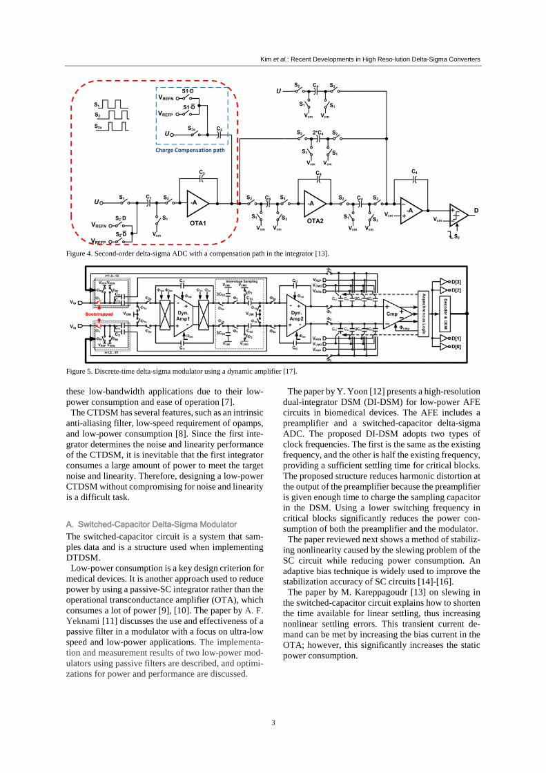
Figure 4. Second-order delta-sigma ADC with a compensation path in the integrator [13].
Figure 5. Discrete-time delta-sigma modulator using a dynamic amplifier [17]. these low-bandwidth applications due to their low-power consumption and ease of operation [7].
The CTDSM has several features, such as an intrinsic anti-aliasing filter, low-speed requirement of opamps, and low-power consumption [8]. Since the first inte-grator determines the noise and linearity performance of the CTDSM, it is inevitable that the first integrator consumes a large amount of power to meet the target noise and linearity. Therefore, designing a low-power CTDSM without compromising for noise and linearity is a difficult task. A. Switched-Capacitor Delta-Sigma Modulator The switched-capacitor circuit is a system that sam-ples data and is a structure used when implementing DTDSM.
Low-power consumption is a key design criterion for medical devices. It is another approach used to reduce power by using a passive-SC integrator rather than the operational transconductance amplifier (OTA), which consumes a lot of power [9], [10]. The paper by A. F. Yeknami [11] discusses the use and effectiveness of a passive filter in a modulator with a focus on ultra-low speed and low-power applications. The implementa-tion and measurement results of two low-power mod-ulators using passive filters are described, and optimi-zations for power and performance are discussed.
The paper by Y. Yoon [12] presents a high-resolution dual-integrator DSM (DI-DSM) for low-power AFE circuits in biomedical devices. The AFE includes a preamplifier and a switched-capacitor delta-sigma ADC. The proposed DI-DSM adopts two types of clock frequencies. The first is the same as the existing frequency, and the other is half the existing frequency, providing a sufficient settling time for critical blocks. The proposed structure reduces harmonic distortion at the output of the preamplifier because the preamplifier is given enough time to charge the sampling capacitor in the DSM. Using a lower switching frequency in critical blocks significantly reduces the power con-sumption of both the preamplifier and the modulator.
The paper reviewed next shows a method of stabiliz-ing nonlinearity caused by the slewing problem of the SC circuit while reducing power consumption. An adaptive bias technique is widely used to improve the stabilization accuracy of SC circuits [14]-[16].
The paper by M. Kareppagoudr [13] on slewing in the switched-capacitor circuit explains how to shorten the time available for linear settling, thus increasing nonlinear settling errors. This transient current de-mand can be met by increasing the bias current in the OTA; however, this significantly increases the static power consumption.

Kim et al.: Recent Developments in High Reso-lution Delta-Sigma Converters
4
Figure 7. Slew-rate enhancement class-AB OTA [18].
Figure 6. Dynamic amplifier during the transferring phase. (a) With-out speeding up. (b) With the speed enhancement branches [17]. A slewing mitigation technique [13] is proposed in which an appropriate amount of charge is provided at the moment of switching the SC circuit so that the
OTA does not need to provide a high peak current. This shows that slewing can be eliminated, and the OTA can be used with less static current for stabiliza-tion accuracy. Figure 4 shows the switched-capacitor single-bit second-order DSM with the charge compen-sation path applied.
The paper by S. Ma [17], which focuses on the mod-ulator, proposes a new dynamic amplifier to realize switched-capacitor integration. The amplifier reset method is used to eliminate the common-mode volt-age drop in the closed-loop dynamic amplifier during the integration phase without using additional load ca-pacitance. Two auxiliary integrators are introduced to improve the integrator’s settling rate. The inter-stage passive sampling network is shown as a dotted line in Figure 5. Figure 6(a) shows the proposed SC integra-tor in the transmission stage with a step voltage input. Figure 6(b) shows the common mode (CM) and dif-ferential mode (DM) coupling effect.
J. Kim [18], applied a slew-rate enhancement class-AB OTA to the first integrator of the SCDSM to im-prove performance. The proposed OTA in this paper adjusts the slew-rate enhancement transistor using an additional common-mode feedback loop, thereby solving the vulnerability of process, voltage, and tem-perature (PVT) fluctuations. Figure 7 shows the slew-rate enhancement class-AB OTA of the first integrator of the SCDSM. If the OTA slew-rate of the first inte-grator and the unity-gain bandwidth (UGBW) are low, harmonics are observed in the digital output spectrum of the SCDSM. For this reason, there is a good perfor-mance improvement by applying the slew-rate en-hancement class-AB OTA to the first SCDSM integra-tor.

Kim et al.: Recent Developments in High Reso-lution Delta-Sigma Converters
5
Figure 8. Proposed hybrid switching integrator [24]. To minimize power consumption, passive integrators are often used. However, passive operation reduces the SNR and causes NTF losses that attenuate the signal along the architecture, making thermal noise dominant [11]. Several active-passive hybrid implementations have been proposed to overcome the reduced loop gain problem in passive DSMs.
A. Hussain [19] describes how to use a low-gain am-plifier and a passive switched-capacitor network to ac-tivate the SC integrator function. Compared to con-ventional opamp-based SC integrators, this solution uses a low-gain open-loop amplifier to drive a passive SC integrator with positive feedback. The open-loop amplifier requires a low DC gain and has exception-ally low-power consumption because it implements an embedded current adder. Power reduction for a single-bit can be achieved using a passive feedforward with a built-in adder to support the first amplifier. The small swing obtained at the output of the active block relieves the slew-rate requirement and improves line-arity.
Next, the DSM based on the SC circuit has issues related to low-supply voltage. The nonlinearity of the input switch becomes more severe at low-supply volt-ages. The previous method used in the design of the low-voltage DSM included clock boosting technology [20], [21], bootstrapped switches [21], a switch RC in-tegrator [22] and a mixed DDA integrator [23]. This technique is effective in increasing the linear range of the switch, but the disadvantage is the additional hard-ware required to generate higher voltage levels.
Y. Yoon [24] demonstrates the use of a hybrid switching integrator to operate at a 0.4V supply volt-age without clock boosting or bootstrapped switches. The circuit proposed in Figure 8 has S1 and S2 switches through the input path. Because these switches are connected to the virtual ground of the OTA, they do not experience cumbersome changes in the switch-on resistance. In addition, all switches transmit a charge at a fixed DC voltage or virtual ground voltage using the SC DAC configuration dur-
ing the 𝜙𝜙2 phase; thus, no distortion occurs. The pro-posed hybrid switching integrator is a DT integrator us-ing resistance. Therefore, the output is similar to the timing of the operation of a mixed DDA integrator. A mixed DDA integrator is susceptible to switching noise because the input signal integration begins at the end of the 𝜙𝜙2 phase, while the proposed integrator begins inte-grating the input signal from the start of the 𝜙𝜙1 phase. Thus it helps overcome the switching noise effect that occurs when the 𝜙𝜙2 phase is completed.
Figure 9. Operation of (a) an active-RC integrator and (b) a Nega-tive-R assisted integrator [6], [35].
Finally, R. Wei [25] introduced a low-power delta-sigma capacitance-to-digital converter (CDC) for ca-pacitive sensors [25]. The input capacitance range is ex-tended by using zoom-in technology with an offset ca-pacitor at the input of the capacitive sensor. Autozero-ing technology is used in the OTA to reduce offset and noise. B. Continuous-Time Delta-Sigma Modulator The initial implementation of the delta-sigma ADC used a CT circuit, but after the SC circuit was devel-oped, it was primarily implemented using SC technol-ogy [5]. However, the recent trend in high-speed ap-plications has shifted the focus back to CT circuits [26]. One of the advantages of the CT circuit is that it does not require a switch; thus, CTDSM can be used for low-voltage designs. Since there is no switch, the stabilization requirements of the amplifier are relaxed, and power consumption can be reduced compared to the DT structure. A power-efficient low-voltage CTDSM is described in [27]. There are several ways

Kim et al.: Recent Developments in High Reso-lution Delta-Sigma Converters
6
to reduce power consumption. Among them, J. L. A. de Melo [28] describes energy and area efficient tech-nologies for the CTDSM. This technique is based on increasing the contribution of a single-bit comparator to the loop-gain by using a passive RC integrator with a low-gain amplifier in a CTDSM loop filter.
Several implementations have been investigated in recent years to improve the energy efficiency of the CTDSM [29]-[34]. A multi-bit quantizer is used mainly to reduce the phase size of the feedback DAC signal [29], [33], [34], and to alleviate the linearity re-quirement of the first integrator. However, the mis-match of the unit elements of the feedback DAC re-quires dynamic element matching (DEM), which lim-its the linearity performance of the CTDSM, increases the design complexity, and leads to higher power con-sumption. In contrast, a single-bit quantizer whose feedback DAC is essentially linear, simplifies the de-sign and reduces power consumption [7], [8], [30]-[32]. M. Jang [6] found that the opamp of the CTDSM in-tegrator has stringent noise and linearity requirements, resulting in large-power losses. Thus, the solution is to reduce the power drastically by applying a negative-R assisted integrator to alleviate the opamp require-ments, including DC gain, UGBW, thermal noise, 1/f noise, and linearity.
Figure 9(a) shows the operation of the active-RC in-tegrator. The finite response of opamp A(s) makes the virtual ground non-ideal (VG=0) and causes current loss Iloss. As a result, the integration current IINT (=IIN-Iloss) loses its size and bandwidth due to the finite gain and bandwidth of the opamp, resulting in the loss of the integrator. In contrast, Figure 9(b) shows the oper-ation of the negative-R assisted integrator. When neg-ative-R is applied to the virtual ground, the compen-sation current Icomp is generated at the ground, cancel-ing Iloss and effectively making the virtual ground ideal (VG=0). Therefore, the integrator’s Iloss due to the opamp’s finite gain and bandwidth is compensated for, and IINT becomes the same as the input current IIN.
An integrator typically has three structures: opamp-RC, OTA-RC, and Gm-C. The opamp-RC integrator has good linearity but has a significant drawback, which is the output swing. To make the output imped-ance small with a complementary metal-oxide semi-conductor (CMOS), a source follower structure must be used. In this case, the output swing increases. The OTA-RC integrator has the advantage of not being af-fected by linearity or parasitic capacitance. The disad-vantage is the finite DC gain. The Gm-C integrator structure has the advantage of being fast, easily adjust-able, and low in current consumption. The disad-vantage is that the coefficient can easily change owing to the influence of nonlinearity and parasitic capaci-tance. The advantages and disadvantages of each
structure mentioned are provided in [5]. D. Basak [36] examines the delta-sigma using the
Gm-C integrator structure. Traditionally, Gm-C-based DSMs are limited in performance due to the nonline-arity of Gm circuits. To obtain sufficient linearity, source degeneration is generally applied to Gm circuits, which inevitably reduces the transconductance and thermal noise efficiency of Gm circuits. Thus, this pa-per [36] presents a new way to change this paradigm. First, a DSM with a passive RC LPF is applied to the feedback. By placing the cut-off frequency of the LPF at the edge of the signal band, the pole of the DSM loop filter reduces the power consumption. The LPF also suppresses the high-frequency component of quantization noise so that quantization noise is not captured in the signal band while using a nonlinear Gm circuit in the feedback of the DSM. By matching the transmission characteristics and inputs, the input and feedback Gm circuits cancel nonlinearity with respect to each other. Second, an integrated input feedback Gm circuit with shared degeneration resistors is proposed, which has high transconductance and noise efficiency and at the same time allows for large input and feed-back signals. L. Lv et al. [37] also used the Gm-C structure design. C. Excess Loop Delay and Clock Jitter Before conducting a detailed analysis of the effects of ELD, the effect of delay on the ELD should be con-sidered. Both the DTDSM and CTDSM have ELDs. This timing error is a problem only in the CTDSM be-cause it is continuously accumulated by the integrator through the DAC of the feedback loop. The ELD in-creases the noise floor and severely reduces the SNR of the DSM [38]. This leads to the instability of the DSM. Even exceedingly small amounts of ELD can cause instability in high-speed modulators [39]. Therefore, it is essential to ensure the stability of the closed-loop DSM. As with all feedback loops, adding a delay reduces the modulator stability. In addition, modulators with higher order or higher out-of-band gain are more sensitive to the effects of excess delay. Finally, because the size of the loop gain does not change according to the delay, the suppression of quantization noise in the signal band should not be af-fected. Fortunately, the serious consequences of delay can be easily solved by adjusting the coefficient of the loop filter and adding a direct path around the quan-tizer [5]. Given the excess delay td, the modified coef-ficient can be easily determined. This paper discusses ways to compensate for these ELD effects as much as possible [40]-[43].
T. He [42] proposes a small delay DSM truncator cir-cuit. The truncator feedback path is merged with an ELD compensation loop that controls the reference se-lection of the internal quantizer. This method solves

Kim et al.: Recent Developments in High Reso-lution Delta-Sigma Converters
7
the ELD problem by embedding a truncator in the dig-ital ELD compensation path without adding to circuit complexity.
Figure 10. (a) CTDSM with a d-cycle of ELD. (b) Theoretical solu-tion for two cycles of ELD compensation using a fast/slow path. (c) Proposed channel coupling for a fast compensation path [41].
S. Kim [43] implemented ELD compensation with a capacitor-based voltage (CV) DAC for ELD compen-sation that is less affected by PVT than modulators us-ing other ELD compensation schemes.
J. Guo [40] presents a new compensation algorithm for the ELD of CTDSM ADC based on a model matching method to improve system performance with the same loop filter. Compared to the previous compensation method, the model matching algorithm is more practical because the ELD values change ran-domly with each clock cycle. Another way to complement ELD is described in [41]. The paper by Y. Hu [41] describes CTDSM using a dual-slope time interleaved quantizer. The ELD of the two sample clocks is compensated using the time in-formation provided through interleaved channel cou-pling. As a result, one full clock cycle is provided for the digital-to-analog conversion dynamic element matching (DEM) operation, allowing for digitally syn-thesized DEM blocks. Figure 10(a) shows the theoret-ical solution for two-cycle ELD compensation using the ELD’s d-cycle, and Figure 10(b) shows the high-speed/low-speed path. In Figure 10(c), because one channel of the time-interleaved quantizer (TIQ) is in
the discharging phase, time information representing the quantized signal value is sampled and transmitted to the other channel. Channel coupling using dual-slope time information can be performed simply by using a current-source turned on or off by dual-slope logic. No additional timing steps or explicit DAC work is required. Since the channel coupling operation directly affects the next sample of TIQ, a rapid ELD compensation loop is realized.
4. Analog Front End The AFE amplifies a small signal and passes it to the DSM. When amplified, noise contained in small sig-nals is also amplified; therefore, care must be taken to remove noise. To implement IA, there are traditionally four topologies: three-opamp IA [44]-[46], current feedback IA [47], resistive feedback IA [48], and ca-pacitively -coupled chopper IA [49].
Figure 11. Instrumentation amplifier [45].
A. The Three-Opamp Instrumentation Amplifier The three-opamp topology has high input impedance and excellent linearity, as demonstrated by [44]-[46]; however, the power efficiency is reduced because two low-noise input amplifiers are required. In addition, the three-opamp IA cannot detect the rail because the input common-mode voltage must also be within the range of the output voltage of the input amplifier. Fig-ure 11 shows the instrumentation amplifier. B. The Current-Feedback Instrumentation Amplifier Current-feedback IA (CFIA) also has high input im-pedance as shown by [47]; however, gain accuracy is limited due to a mismatch between input and feedback transconductance. Figure 12 shows the current feed-back instrumentation amplifier. The CFIA can have a rail detection function using an n-channel metal-oxide semiconductor (NMOS) or p-channel metal-oxide semiconductor (PMOS) based input differential; how-ever, it is very difficult to achieve the rail-to-rail input
Kim et al.: Recent Developments in High Reso-lution Delta-Sigma Converters
8
function with high gain accuracy because the mis-match between the input and feedback transconduct-ance is generally also a function of the input CM volt-age. The power efficiency of CFIA is also limited by the need for two input and feedback transconduct-ances.
C. Lee [50] presented low-noise, low-power, chop-per-stabilization, and a CFIA for biopotential signal acquisition applications. The design used includes an AC coupled chopper stabilization CFIA to reduce 1/f noise. It also uses a switched-capacitor integrator to reduce the input offset and provide high accuracy.
Figure 12. Schematic of the current-feedback instrumentation am-plifier [47]. C. The Resistive-Feedback Instrumentation Amplifier Resistive-feedback IA topology is the third option, however, as noted in [48], the value of the input re-sistance is a trade-off between noise and input imped-ance. Finally, the closed-loop gain of the three topol-ogies is defined by the resistive network loading the output stage of the IA [51]-[54]. Increasing the re-sistance of the network leads to a larger chip area and more noise.
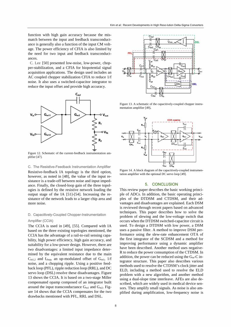
D. Capacitively-Coupled Chopper-Instrumentation Amplifier (CCIA) The CCIA is used in [49], [55]. Compared with IA based on the three existing topologies mentioned, the CCIA has the advantage of a rail-to-rail sensing capa-bility, high power efficiency, high gain accuracy, and suitability for a low-power design. However, there are two disadvantages: a limited input impedance deter-mined by the equivalent resistance due to the main Cin1,2 and fchop, an up-modulated offset of Gm1, 1/f noise, and a chopping ripple. Using a positive feed-back loop (PFL), ripple reduction loop (RRL), and DC servo loop (DSL) resolve these disadvantages. Figure 13 shows the CCIA. It is based on a two-stage Miller compensated opamp composed of an integrator built around the input transconductance Gm1 and Gm2. Fig-ure 14 shows that the CCIA compensates for the two drawbacks mentioned with PFL, RRL and DSL.
Figure 13. A schematic of the capacitively-coupled chopper instru-mentation amplifier [49].
Figure 14. A block diagram of the capacitively-coupled instrumen-tation amplifier with the optional DC servo loop [49].
5. CONCLUSION This review paper describes the basic working princi-ple of ADCs. In addition, the basic operating princi-ples of the DTDSM and CTDSM, and their ad-vantages and disadvantages are explained. Each DSM is reviewed through recent papers based on advanced techniques. This paper describes how to solve the problem of slewing and the low-voltage switch that occurs when the DTDSM switched-capacitor circuit is used. To design a DTDSM with low power, a DSM uses a passive filter. A method to improve DSM per-formance using the slew-rate enhancement OTA of the first integrator of the SCDSM and a method for improving performance using a dynamic amplifier have been described. Another method uses negative-R to reduce the power consumption of the CTDSM. In addition, the power can be reduced using the Gm-C in-tegrator structure. This paper also describes various methods used to resolve the CTDSM’s clock jitter and ELD, including a method used to resolve the ELD problem with a new algorithm, and another method using a dual-slope time interleave. AFEs are also de-scribed, which are widely used in medical device sen-sors. They amplify small signals. As noise is also am-plified during amplification, low-frequency noise is

Kim et al.: Recent Developments in High Reso-lution Delta-Sigma Converters
9
removed using chopper-stabilization techniques. The AFE is described based on the advantages and disad-vantages of the 3-opamp IA, CFIA (current feedback IA), resistive feedback IA and capacitively coupled IA (CCIA) methods.
ACKNOWLEDGMENT This work was supported by the National Research Foundation of Korea (NRF) grant funded by the Korea government (MSIT) (No. 202000000001166). This research was also supported by the MSIT (Ministry of Science and ICT), Korea, under the ITRC (Infor-mation Technology Research Center) support pro-gram (IITP-2020-2018-0-01421) supervised by the IITP (Institute of Information & communications Technology Planning & Evaluation).
REFERENCES [1] G. Chen, S. Hanson, D. Blaauw and D. Sylvester, "Circuit De-
sign Advances for Wireless Sensing Applications," in Pro-ceedings of the IEEE, vol. 98, no. 11, pp. 1808-1827, Nov. 2010.
[2] Y. Tachwali, H. Refai and J. E. Fagan, "Minimizing HVAC Energy Consumption Using a Wireless Sensor Network," IE-CON 2007 - 33rd Annual Conference of the IEEE Industrial Electronics Society, Taipei, pp. 439-444, Nov. 2007.
[3] S. Drago, D. M. W. Leenaerts, B. Nauta, F. Sebastiano, K. A. A. Makinwa and L. J. Breems. "A 200 μA Duty-Cycled PLL for Wireless Sensor Nodes in 65 nm CMOS," in IEEE Journal of Solid-State Circuits, vol. 45, no. 7, pp. 1305-1315, Jul. 2010.
[4] T. C. Carusone, D. A. Johns and K. W. Martin, Analog Inte-grated Circuit Design, 2nd Edition, WILEY, 2012
[5] S. Pavan, R. Schreier, G. C. Temes, Understanding Delta-Sigma Data Converters. 2nd ed. New York, NY: Wiley; 2017.
[6] M. Jang, C. Lee and Y. Chae, "Analysis and Design of Low-Power Continuous-Time Delta-Sigma Modulator Using Nega-tive-R Assisted Integrator," in IEEE Journal of Solid-State Circuits, vol. 54, no. 1, pp. 277-287, Jan. 2019.
[7] A. Sukumaran and S. Pavan, "Low Power Design Techniques for Single-Bit Audio Continuous-Time Delta Sigma ADCs Using FIR Feedback," in IEEE Journal of Solid-State Cir-cuits, vol. 49, no. 11, pp. 2515-2525, Nov. 2014.
[8] S. Pavan and P. Sankar, "Power Reduction in Continuous-Time Delta-Sigma Modulators Using the Assisted Opamp Tech-nique," in IEEE Journal of Solid-State Circuits, vol. 45, no. 7, pp. 1365-1379, Jul. 2010.
[9] F. Chen and B. Leung, "A 0.25-mW Low-Pass Passive Sigma-Delta Modulator with Built-in Mixer for a 10-MHz IF Input," in IEEE Journal of Solid-State Circuits, vol. 32, no. 6, pp. 774-782, Jun. 1997.
[10] R. Yousry, E. Hegazi and H. F. Ragai, "A Third-Order 9-Bit 10-MHz CMOS Delta-Sigma Modulator with One Active Stage," in IEEE Transactions on Circuits and Systems I: Reg-ular Papers, vol. 55, no. 9, pp. 2469-2482, Oct. 2008.
[11] A. F. Yeknami, F. Qazi and A. Alvandpour, "Low-Power DT Delta-Sigma Modulators Using SC Passive Filters in 65 nm CMOS," in IEEE Transactions on Circuits and Systems I: Regular Papers, vol. 61, no. 2, pp. 358-370, Feb. 2014.
[12] Y. Yoon, Q. Duan, J. Yeo, J. Roh, J. Kim and D. Kim, "A Delta–Sigma Modulator for Low-Power Analog Front Ends in Biomedical Instrumentation," in IEEE Transactions on In-strumentation and Measurement, vol. 65, no. 7, pp. 1530-1539, Jul. 2016.
[13] M. Kareppagoudr, J. Shakya, E. Caceres, Y. -W. Kuo and G. C. Temes, "Slewing Mitigation Technique for Switched Ca-
pacitor Circuits," in IEEE Transactions on Circuits and Sys-tems I: Regular Papers, vol. 67, no. 10, pp. 3251-3261, Oct. 2020.
[14] M. P. Garde, A. Lopez-Martin, R. G. Carvajal and J. Ramí-rez-Angulo, "Super Class-AB Recycling Folded Cascode OTA," in IEEE Journal of Solid-State Circuits, vol. 53, no. 9, pp. 2614-2623, Sept. 2018.
[15] Y. Jing and B. Bakkaloglu, "A High Slew-Rate Adaptive Bi-asing Hybrid Envelope Tracking Supply Modulator for LTE Applications," in IEEE Transactions on Microwave Theory and Techniques, vol. 65, no. 9, pp. 3245-3256, Sept. 2017.
[16] H. He, T. Ge, Y. Kang, L. Guo and J. S. Chang, "A 40 MHz Bandwidth, 91% Peak Efficiency, 2.5 W Output Power Sup-ply Modulator with Dual-Mode Sigma–Delta Control and Adaptive Biasing Amplifier for Multistandard Communica-tions," in IEEE Transactions on Power Electronics, vol. 35, no. 9, pp. 9430-9442, Sept. 2020.
[17] S. Ma, L. Liu, T. Fang, J. Liu and N. Wu, "A Discrete-Time Audio Delta-Sigma Modulator Using Dynamic Amplifier with Speed Enhancement and Flicker Noise Reduction Tech-niques," in IEEE Journal of Solid-State Circuits, vol. 55, no. 2, pp. 333-343, Feb. 2020.
[18] J. Kim, S. Song and J. Roh, "A High Slew-Rate Enhancement Class-AB Operational Transconductance Amplifier (OTA) for Switched-Capacitor (SC) Application," in IEEE Access, 2020.
[19] A. Hussain, S. Sin, C. Chan, S. Ben U, F. Maloberti and R. P. Martins, "Active–Passive Delta-Sigma Modulator for High-Resolution and Low-Power Applications," in IEEE Transac-tions on Very Large Scale Integration (VLSI) Systems, vol. 25, no. 1, pp. 364-374, Jan. 2017.
[20] F. Michel and M. S. J. Steyaert, "A 250 mV 7.5 μW 61 dB SNDR SC ΔΣ Modulator Using Near-Threshold-Voltage-Bi-ased Inverter Amplifiers in 130 nm CMOS," in IEEE Journal of Solid-State Circuits, vol. 47, no. 3, pp. 709-721, Mar. 2012.
[21] Z. Yang, L. Yao and Y. Lian, "A 0.5-V 35-μW 85-dB DR Double-Sampled Delta-Sigma Modulator for Audio Applica-tions," in IEEE Journal of Solid-State Circuits, vol. 47, no. 3, pp. 722-735, Mar. 2012.
[22] G. Ahn, "A 0.6-V 82-dB Delta-Sigma Audio ADC Using Switched-RC Integrators," in IEEE Journal of Solid-State Cir-cuits, vol. 40, no. 12, pp. 2398-2407, Dec. 2005.
[23] Y. Yoon, H. Roh and J. Roh, "A True 0.4-V Delta–Sigma Modulator Using a Mixed DDA Integrator Without Clock Boosted Switches," in IEEE Transactions on Circuits and Sys-tems II: Express Briefs, vol. 61, no. 4, pp. 229-233, Apr. 2014.
[24] Y. Yoon, D. Choi and J. Roh, "A 0.4 V 63 µW 76.1 dB SNDR 20 kHz Bandwidth Delta-Sigma Modulator Using a Hybrid Switching Integrator," in IEEE Journal of Solid-State Circuits, vol. 50, no. 10, pp. 2342-2352, Oct. 2015.
[25] R. Wei, W. Wang, X. Xiao and Q. Chen, "A Low-Power Delta-Sigma Capacitance-to-Digital Converter for Capacitive Sensors," in IEEE Access, vol. 7, pp. 78281-78288, Jun. 2019.
[26] C. Ho, C. Liu, C. Lo, H. Tsai, T. Wang and Y. Lin, "A 4.5 mW CT Self-Coupled Delta-Sigma Modulator with 2.2 MHz BW and 90.4 dB SNDR Using Residual ELD Compensation," in IEEE Journal of Solid-State Circuits, vol. 50, no. 12, pp. 2870-2879, Dec. 2015.
[27] J. Zhang, Y. Lian, L. Yao and B. Shi, "A 0.6-V 82-dB 28.6- µW Continuous-Time Audio Delta-Sigma Modulator," in IEEE Journal of Solid-State Circuits, vol. 46, no. 10, pp. 2326-2335, Oct. 2011.
[28] J. L. A. de Melo, N. Paulino and J. Goes, "Continuous-Time Delta-Sigma Modulators Based on Passive RC Integrators," in IEEE Transactions on Circuits and Systems I: Regular Pa-pers, vol. 65, no. 11, pp. 3662-3674, Nov. 2018.
[29] S. Pavan, N. Krishnapura, R. Pandarinathan and P. Sankar, "A Power Optimized Continuous-Time Delta-Sigma ADC for Audio Applications," in IEEE Journal of Solid-State Circuits, vol. 43, no. 2, pp. 351-360, Feb. 2008.
[30] S. Loeda, J. Harrison, F. Pourchet and A. Adams, "A 10/20/30/40 MHz Feedforward FIR DAC Continuous-Time Delta-Sigma ADC with Robust Blocker Performance for Ra-dio Receivers," in IEEE Journal of Solid-State Circuits, vol. 51, no. 4, pp. 860-870, Apr. 2016.

Kim et al.: Recent Developments in High Reso-lution Delta-Sigma Converters
10
[31] P. Shettigar and S. Pavan, "Design Techniques for Wideband Single-Bit Continuous-Time Delta-Sigma Modulators with FIR Feedback DACs," in IEEE Journal of Solid-State Cir-cuits, vol. 47, no. 12, pp. 2865-2879, Dec. 2012.
[32] S. Billa, A. Sukumaran and S. Pavan, "Analysis and Design of Continuous-Time Delta–Sigma Converters Incorporating Chopping," in IEEE Journal of Solid-State Circuits, vol. 52, no. 9, pp. 2350-2361, Sept. 2017.
[33] Y. H. Leow, H. Tang, Z. C. Sun and L. Siek, "A 1 V 103 dB 3rd-Order Audio Continuous-Time Delta-Sigma ADC with Enhanced Noise Shaping in 65 nm CMOS," in IEEE Journal of Solid-State Circuits, vol. 51, no. 11, pp. 2625-2638, Nov. 2016.
[34] C. De Berti, P. Malcovati, L. Crespi and A. Baschirotto, "A 106 dB A-Weighted DR Low-Power Continuous-Time Sigma-Delta Modulator for MEMS Microphones," in IEEE Journal of Solid-State Circuits, vol. 51, no. 7, pp. 1607-1618, Jul. 2016.
[35] M. Jang, C. Lee and Y. Chae, "A 134-μW 99.4-dB SNDR Audio Continuous-Time Delta-Sigma Modulator with Chopped Negative-R and Tri-Level FIR-DAC," in IEEE Jour-nal of Solid-State Circuits, Nov. 2020.
[36] D. Basak, D. Li and K. Pun, "A Gm-C Delta-Sigma Modula tor with a Merged Input-Feedback Gm Circuit for Nonlinear-ity Cancellation and Power Efficiency Enhancement," in IEEE Transactions on Circuits and Systems I: Regular Pa-pers, vol. 65, no. 4, pp. 1196-1209, Apr. 2018.
[37] L. Lv, A. Jain, X. Zhou, J. Becker, Q. Li and M. Ortmanns, "A 0.4-V Gm-C Proportional-Integrator-Based Continuous-Time Delta-Sigma Modulator with 50-kHz BW and 74.4-dB SNDR," in IEEE Journal of Solid-State Circuits, vol. 53, no. 11, pp. 3256-3267, Nov. 2018.
[38] J. A. Cherry and W. M. Snelgrove, "Excess Loop Delay in Continuous-Time Delta-Sigma Modulators," in IEEE Trans-actions on Circuits and Systems II: Analog and Digital Signal Processing, vol. 46, no. 4, pp. 376-389, Apr. 1999.
[39] K. El-Sankary, H. H. Alamdari and E. I. El-Masry, "An Adaptive ELD Compensation Technique Using a Predictive Comparator," in IEEE Transactions on Circuits and Systems II: Express Briefs, vol. 56, no. 8, pp. 619-623, Aug. 2009.
[40] J. Guo and M. E. Magaña, "Compensation Method of The Ex-cess Loop Delay in Continuous-Time Delta-Sigma Analog-to-Digital Converters Based on Model Matching Approach," in IET Circuits, Devices & Systems, vol. 10, no. 1, pp. 29-36, Jan. 2016.
[41] Y. Hu, H. Venkatram, N. Maghari and U. Moon, "A Continu ous-Time Delta-Sigma ADC Utilizing Time Information for Two Cycles of Excess Loop Delay Compensation," in IEEE Transactions on Circuits and Systems II: Express Briefs, vol. 62, no. 11, pp. 1063-1067, Nov. 2015.
[42] T. He, Y. Zhang and G. C. Temes, "Digital Excess Loop De-lay Compensation Technique with Embedded Truncator for Continuous-Time Delta–Sigma Modulators," in Electronics Letters, vol. 52, no. 1, pp. 20-21, Jan. 2016.
[43] S. Kim, S. Na, Y. Yang and S. Kim, "A 2-MHz BW 82-dB DR Continuous-Time Delta–Sigma Modulator with a Capaci-tor-Based Voltage DAC for ELD Compensation," in IEEE Transactions on Very Large Scale Integration (VLSI) Systems, vol. 26, no. 10, pp. 1999-2006, Oct. 2018.
[44] M. J. Burke and D. T. Gleeson, "A Micropower Dry-Elec-trode ECG Preamplifier," in IEEE Transactions on Biomedi-cal Engineering, vol. 47, no. 2, pp. 155-162, Feb. 2000.
[45] E. M. Spinelli, R. Pallas-Areny and M. A. Mayosky, "AC-Coupled Front-End for Biopotential Measurements," in IEEE Transactions on Biomedical Engineering, vol. 50, no. 3, pp. 391-395, Mar. 2003.
[46] E. M. Spinelli, N. Martinez, M. A. Mayosky and R. Pallas-Areny, "A Novel Fully Differential Biopotential Amplifier with DC Suppression," in IEEE Transactions on Biomedical Engineering, vol. 51, no. 8, pp. 1444-1448, Aug. 2004.
[47] R. Wu, K. A. A. Makinwa and J. H. Huijsing, "A Chopper Current-Feedback Instrumentation Amplifier with a 1mHz 1/ƒ Noise Corner and An AC-Coupled Ripple-Reduction
Loop," 2009 IEEE International Solid-State Circuits Confer-ence - Digest of Technical Papers, San Francisco, CA, pp. 322-323,323a, Feb. 2009.
[48] J. H. Huijsing, Operational Amplifier: Theory and Design. Boston, MA: Kluwer Academic, 2001.
[49] Q. Fan, F. Sebastiano, J. H. Huijsing and K. A. A. Makinwa, "A 1.8 µW 60 nV √ Hz Capacitively-Coupled Chopper Instru-mentation Amplifier in 65 nm CMOS for Wireless Sensor Nodes," in IEEE Journal of Solid-State Circuits, vol. 46, no. 7, pp. 1534-1543, Jul. 2011.
[50] C. Lee and J. Song, "A Chopper Stabilized Current-Feedback Instrumentation Amplifier for EEG Acquisition Applications," in IEEE Access, vol. 7, pp. 11565-11569, Jan. 2019.
[51] T. Denison, K. Consoer, W. Santa, A. Avestruz, J. Cooley and A. Kelly, "A 2 µW 100 nV/rtHz Chopper-Stabilized In-strumentation Amplifier for Chronic Measurement of Neural Field Potentials," in IEEE Journal of Solid-State Circuits, vol. 42, no. 12, pp. 2934-2945, Dec. 2007.
[52] N. Verma, A. Shoeb, J. Bohorquez, J. Dawson, J. Guttag and A. P. Chandrakasan, "A Micro-Power EEG Acquisition SoC with Integrated Feature Extraction Processor for a Chronic Seizure Detection System," in IEEE Journal of Solid-State Circuits, vol. 45, no. 4, pp. 804-816, Apr. 2010.
[53] R. R. Harrison and C. Charles, "A Low-Power Low-Noise CMOS Amplifier for Neural Recording Applications," in IEEE Journal of Solid-State Circuits, vol. 38, no. 6, pp. 958-965, Jun. 2003.
[54] D. Yeager, F. Zhang, A. Zarrasvand, N. T. George, T. Daniel and B. P. Otis, "A 9 µA, Addressable Gen2 Sensor Tag for Bi-osignal Acquisition," in IEEE Journal of Solid-State Circuits, vol. 45, no. 10, pp. 2198-2209, Oct. 2010.
[55] H. Jiang, C. Ligouras, S. Nihtianov and K. A. A. Makinwa, "A 4.5 nV/√Hz Capacitively Coupled Continuous-Time Sigma-Delta Modulator with an Energy-Efficient Chopping Scheme," in IEEE Solid-State Circuits Letters, vol. 1, no. 1, pp. 18-21, Jan. 2018.
AUTHOR BIOGRAPHIES Jaedo Kim received the B.S. degree in electrical and electronic engineering from Hanyang University, Ansan, South Korea, in 2019, where he is cur-rently working towards a Ph.D. degree. His current research interests include low-power oversampled delta-sigma
converters and mixed-integrated circuits.
Jeongjin Roh (Senior Member, IEEE) received the B.S degree in electrical engineering from the Hanyang Univer-sity, Seoul, Korea, in 1990, the M.S. degree in electrical engineering from the Pennsylvania State University in 1998, and the Ph.D. degree in com-
puter engineering from the University of Texas at Austin in 2001. From 1990 to 1996, he was with the Samsung Electronics, Giheung, Korea, as a senior cir-cuit designer for mixed-signal products. From 2000 to 2001, he was with the Intel Corporation, Austin, Texas, as a senior analog designer for delta-sigma data con-verters. In 2001, he joined the faculty of the Hanyang University, Ansan, Korea. His research interests in-clude power management circuits and oversampled delta-sigma converters.
Author’s photo (3*2)
Author’s photo (3*2)